JP2004111435A - Electric/electronic module having integral molding structure of connector and electronic part and method for molding the same - Google Patents
Electric/electronic module having integral molding structure of connector and electronic part and method for molding the same Download PDFInfo
- Publication number
- JP2004111435A JP2004111435A JP2002268201A JP2002268201A JP2004111435A JP 2004111435 A JP2004111435 A JP 2004111435A JP 2002268201 A JP2002268201 A JP 2002268201A JP 2002268201 A JP2002268201 A JP 2002268201A JP 2004111435 A JP2004111435 A JP 2004111435A
- Authority
- JP
- Japan
- Prior art keywords
- electronic
- resin
- electric
- circuit board
- electronic circuit
- Prior art date
- Legal status (The legal status is an assumption and is not a legal conclusion. Google has not performed a legal analysis and makes no representation as to the accuracy of the status listed.)
- Granted
Links
Images


Classifications
-
- H—ELECTRICITY
- H05—ELECTRIC TECHNIQUES NOT OTHERWISE PROVIDED FOR
- H05K—PRINTED CIRCUITS; CASINGS OR CONSTRUCTIONAL DETAILS OF ELECTRIC APPARATUS; MANUFACTURE OF ASSEMBLAGES OF ELECTRICAL COMPONENTS
- H05K5/00—Casings, cabinets or drawers for electric apparatus
- H05K5/0026—Casings, cabinets or drawers for electric apparatus provided with connectors and printed circuit boards [PCB], e.g. automotive electronic control units
- H05K5/0034—Casings, cabinets or drawers for electric apparatus provided with connectors and printed circuit boards [PCB], e.g. automotive electronic control units having an overmolded housing covering the PCB
-
- H—ELECTRICITY
- H01—ELECTRIC ELEMENTS
- H01L—SEMICONDUCTOR DEVICES NOT COVERED BY CLASS H10
- H01L2224/00—Indexing scheme for arrangements for connecting or disconnecting semiconductor or solid-state bodies and methods related thereto as covered by H01L24/00
- H01L2224/01—Means for bonding being attached to, or being formed on, the surface to be connected, e.g. chip-to-package, die-attach, "first-level" interconnects; Manufacturing methods related thereto
- H01L2224/42—Wire connectors; Manufacturing methods related thereto
- H01L2224/44—Structure, shape, material or disposition of the wire connectors prior to the connecting process
- H01L2224/45—Structure, shape, material or disposition of the wire connectors prior to the connecting process of an individual wire connector
- H01L2224/45001—Core members of the connector
- H01L2224/45099—Material
- H01L2224/451—Material with a principal constituent of the material being a metal or a metalloid, e.g. boron (B), silicon (Si), germanium (Ge), arsenic (As), antimony (Sb), tellurium (Te) and polonium (Po), and alloys thereof
- H01L2224/45138—Material with a principal constituent of the material being a metal or a metalloid, e.g. boron (B), silicon (Si), germanium (Ge), arsenic (As), antimony (Sb), tellurium (Te) and polonium (Po), and alloys thereof the principal constituent melting at a temperature of greater than or equal to 950°C and less than 1550°C
- H01L2224/45144—Gold (Au) as principal constituent
-
- H—ELECTRICITY
- H01—ELECTRIC ELEMENTS
- H01L—SEMICONDUCTOR DEVICES NOT COVERED BY CLASS H10
- H01L2224/00—Indexing scheme for arrangements for connecting or disconnecting semiconductor or solid-state bodies and methods related thereto as covered by H01L24/00
- H01L2224/01—Means for bonding being attached to, or being formed on, the surface to be connected, e.g. chip-to-package, die-attach, "first-level" interconnects; Manufacturing methods related thereto
- H01L2224/42—Wire connectors; Manufacturing methods related thereto
- H01L2224/47—Structure, shape, material or disposition of the wire connectors after the connecting process
- H01L2224/48—Structure, shape, material or disposition of the wire connectors after the connecting process of an individual wire connector
- H01L2224/4805—Shape
- H01L2224/4809—Loop shape
- H01L2224/48091—Arched
-
- H—ELECTRICITY
- H01—ELECTRIC ELEMENTS
- H01L—SEMICONDUCTOR DEVICES NOT COVERED BY CLASS H10
- H01L2224/00—Indexing scheme for arrangements for connecting or disconnecting semiconductor or solid-state bodies and methods related thereto as covered by H01L24/00
- H01L2224/01—Means for bonding being attached to, or being formed on, the surface to be connected, e.g. chip-to-package, die-attach, "first-level" interconnects; Manufacturing methods related thereto
- H01L2224/42—Wire connectors; Manufacturing methods related thereto
- H01L2224/47—Structure, shape, material or disposition of the wire connectors after the connecting process
- H01L2224/48—Structure, shape, material or disposition of the wire connectors after the connecting process of an individual wire connector
- H01L2224/481—Disposition
- H01L2224/48135—Connecting between different semiconductor or solid-state bodies, i.e. chip-to-chip
- H01L2224/48137—Connecting between different semiconductor or solid-state bodies, i.e. chip-to-chip the bodies being arranged next to each other, e.g. on a common substrate
-
- H—ELECTRICITY
- H01—ELECTRIC ELEMENTS
- H01L—SEMICONDUCTOR DEVICES NOT COVERED BY CLASS H10
- H01L2924/00—Indexing scheme for arrangements or methods for connecting or disconnecting semiconductor or solid-state bodies as covered by H01L24/00
- H01L2924/19—Details of hybrid assemblies other than the semiconductor or other solid state devices to be connected
- H01L2924/191—Disposition
- H01L2924/19101—Disposition of discrete passive components
- H01L2924/19107—Disposition of discrete passive components off-chip wires
Abstract
Description
【0001】
【発明の属する技術分野】
本発明は、少なくとも接続用金属端子を有するコネクタ、セラミックや有機樹脂または樹脂プリントの電子回路基板上に実装された電子部品、該電子部品を封止する樹脂、及び該電子回路基板とコネクタとを電気的に接続する金属リードまたはワイヤ若しくは可撓性の導体等の接続線からなる電気・電子モジュールを、低熱膨張性及び低吸湿性の樹脂成形材料を用いて一体成形し、少なくとも該コネクタの基板との接続面側と電子部品との封止を同時に行うことによって達成できる低コストで、しかも高信頼性の電気・電子モジュールとその成形方法に関する。
【0002】
【従来の技術】
自動車の各種コントロールユニット及びセンサーモジュールは、電子回路を搭載したセラミック乃至樹脂の電子回路基板、入出力コネクタ部を有する金属またはプラスチックケース、及び/またはキャップからなる構造を有する。これらの構造の中には、半導体チップの放熱性を向上させるために、放熱用金属ベース上に前記のセラミック乃至樹脂の電子回路基板を搭載する構造も含まれる。
【0003】
コントロールユニットの従来技術例として、図5にセラミックの電子回路基板を用いたエンジンコントロールユニットの構造を示す。セラミックの電子回路基板1上にコンデンサ、及び抵抗体などの各種チップ部品3と半導体ベアチップ4を搭載した後、ワイヤボンデイング5や半田などによってセラミックの電子回路基板の表層導体と接合する。このセラミックの電子回路基板1を筐体であるプラスチック製または金属製コネクタ7と一体になっている金属放熱板6上に搭載、接着する。セラミックの電子回路基板1の接続用パッドとコネクタの端子リードはワイヤボンデイング9、半田、TAB(テープオートメイテイドボンデイング)などの方法によって接合を行い、電気的な導通を取っている。その後、シリコーンゲル20を塗布、加熱することによって上記の各種電子部品を、外気雰囲気からの湿度または異物付着の影響から保護している。最終的にキャップ23が接着剤またはOリング状のゴムを用いて、上記の筐体に固着または加締めにより取り付けられる。
【0004】
図6と図7には、従来の樹脂成形タイプ電子回路装置を示す。図6は、特開平9−45851号公報や特開平2001−326303号公報に記載されているように、半導体パワーモジュールなどで採用されている構造であり、放熱金属板6、導体パターン、複数の電子部品(パワー半導体素子24と制御用集積回路素子25)、放熱板取り付け用プラスチックケースまたはコネクタ7、及びエポキシ樹脂などの保護樹脂26から構成されている。
【0005】
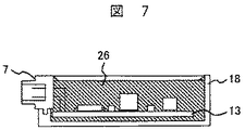
一方、図7は自動車または民生用で採用されている電子回路装置の構造であり、上面と前面が開口され、かつ左右に取り付け部を有するプラスチックケース18、電子部品を搭載した樹脂回路基板13、外部接続端子となるコネクタ7からなり、コネクタはケースの前面に取り付けられる。図7に示す保護樹脂26は電子部品及び電子回路基板を外部の湿気から保護、及び振動に対する固定のための保護層である。電子部品を搭載した電子回路基板をコネクタの外部端子部とはんだ付けなどにより接続し、樹脂の電子回路基板をケースに位置決めとともに取り付けを行った後、液状樹脂を注入、加熱硬化して保護樹脂を形成する。
【0006】
また、図8に、特許第3149678号公報に記載の圧力センサーモジュールの構造を示す。ガラス台15の上にダイヤフラム部17を下向きにしてセンサーチップ16を搭載し、真空雰囲気中で両者間を陽極接合または半田付けにより気密接合する。これを外部端子を有する樹脂ケース内18の底面に接着剤で接着し、センサーチップと外部端子とを金属ワイヤ線9でボンデイングした後、シリコーンゲル20を注入塗布してセンサーチップ及び金属ワイヤの表面を封止する。その後、導圧孔22、及び外部接続用コネクタ端子を備えた樹脂ケース内に収納し、かつセンサーチップを組み込んだ樹脂ケースより引き出した外部リード19を外ケースのコネクタ端子8によって溶接接続した後、測定圧の導圧空間を除いて外ケースの開放面と前記樹脂ケースとの空間を封止樹脂26で充填することによって組立て構成する。
【0007】
【発明が解決しようとする課題】
従来の構造は上記に示すように、電子部品が搭載された電子回路基板、この電子回路基板と電気的に接続した接続用金属端子を有するコネクタ、電子回路基板を収納するケース、シリコーンゲルやエポキシ樹脂などの保護樹脂及び/またはキャップを有することが、次のような問題がある。
【0008】
自動車は居住性向上の観点から、エンジンルームは狭くして車室空間を広くする傾向にある。そのため、コントロールユニットに対しても小型化、薄型化が求められるようになったが、従来の構造はケースに電子回路基板を収納する構造であるために、モジュールが大きく、かつ厚くなる傾向にあり、この要求を満足できなくなっている。
【0009】
この問題を改善するために、図9の(a)に示すような電子回路基板とコネクタとを一体的に結合する樹脂形成タイプの電子回路装置が特開平7−22722号公報に記載されている。この公報では、図9の(b)に示すように、保護樹脂の形成方法として、真空状態に保った型内にペースト状樹脂を流し込んだ後、加熱硬化する低圧成形法が提案されている。
【0010】
しかし、この方法は真空状態を保つための特別な型構造や装置が必要であること、保護樹脂としてペースト状樹脂を用いるために、硬化時間が数十分以上となり、製品を型から取り出すまでの時間が長くなること、が問題である。
【0011】
さらに、電子回路基板や電子部品と熱膨張係数を合わせた保護樹脂は、硬化前のペースト状の樹脂粘度が非常に高くなるため、樹脂注入に対して高真空が必要であり、生産性が劣る。
【0012】
また、放熱用の金属板上に電子回路基板や電子回路を搭載する電子回路装置では、コネクタや放熱用金属板の位置決めが難しいため、実質上、真空低圧成形法が困難になる。さらに、圧力測定用の導圧孔を有する圧力センサーにおいても、センサー形状の点から真空状態を保つため、型構造が複雑となったり、センサーの外部ケースの位置決めが困難になる。
【0013】
本発明は、上記の点に鑑みてなされたものであり、電子回路基板や電子部品を被覆する保護層(樹脂層)としての樹脂の熱硬化時間が早くて量産性に優れ、かつ高真空に保たなくとも樹脂注入ができる電子部品の一体モールド構造を有する電気・電子モジュールを提供せんとするものである。
【0014】
また、本発明は、電子回路装置の信頼性向上、小型軽量化、並びに低コスト化のための部材及び工数低減を図るために、低熱膨張性低吸湿性、及び高接着性の樹脂成形材料を用いて加熱加圧下による一体成形を行い、電子部品を搭載した回路基板と、少なくとも該コネクタの基板との接続面側との封止を同時に行う電気・電子モジュールとその成形方法を提供することにある。
【0015】
【課題を解決するための手段】
本発明は、コネクタ、電子部品、および電子回路基板を被覆する熱硬化性の樹脂層とを含む電子部品の一体モールド構造を有する電気・電子モジュールにあって、前記樹脂層の樹脂は熱硬化前の形態が40℃以下の温度において固形であることを特徴とするものである。
【0016】
更に具体的に述べる。
【0017】
本発明においては、電子回路基板上に実装した電子部品及び、少なくともコネクタを電子回路基板に取り付けるところの取り付け部側(接続面側)に配置した金属リード、ワイヤ、フレキシブルな接続用導体等の接続線を完全に覆い隠すように封止するために用いる樹脂が、無機質フィラを含む40℃以下において固形のエポキシ樹脂成形材料であることを特徴としており、通常の樹脂封止型半導体装置用封止材料と同じものを使用することができる。この固形のエポキシ樹脂成形材料は、加熱加圧下による一体成形を行うには最も適した封止樹脂であり、成形性と電気・電子モジュールの信頼性を同時に確保することができる。
【0018】
さらに、このエポキシ樹脂成形材料(熱硬化樹脂)はポリブチレンテレフタレート、ナイロン、またはポリフェニレンサルファイドからなる熱可塑性樹脂で作られているコネクタとの接着性にも優れ、耐久試験において懸念される金属リード、ワイヤ、フレキシブルな接続用導体等の接続線の断線や剥離(電子回路基板、電子部品、接続線、コネクタ等と樹脂の剥離)は見られないため、信頼性向上には大きな効果がある。前記接着性が向上した理由のひとつとしては、成形温度が150〜180℃であるため、コネクタの樹脂とエポキシ樹脂との境界面に分子の絡まり合いが生じて強固な接着界面を形成することが挙げられる。エポキシ樹脂成形材料に含まれる無機質フィラとしては、溶融シリカ、結晶性シリカ、アルミナ、酸化マグネシウムなどの破砕状または球状の少なくとも1種類以上を用いることができる。エポキシ樹脂成形材料としては、エポキシ樹脂とフェノール樹脂硬化剤とからなる組成であり、40℃以下で固形のオルソクレゾール型エポキシ樹脂、ビフェニル骨格を有するエポキシ樹脂、ジシクロペンタジエン骨格を有するエポキシ樹脂、ナフタレン骨格を有するエポキシ樹脂またはビスフェノールA型エポキシ樹脂などと、フェノールノボラック樹脂、オルソクレゾールノボラック樹脂、ジシクロペンタジエン骨格を有するフェノール樹脂、またはナフタレン骨格を有するフェノール樹脂などとの組み合わせから得ることができる。また、エポキシ樹脂成形材料には低弾性率化による低応力化を図るため、シリコーンゴムまたはオイルやブタジエン系ゴムなどの低応力化材を含むことができる。
【0019】
本発明では、電子回路基板上に実装した電子部品及び、少なくともコネクタを電子回路基板に取り付けるところの取り付け部側(接続面側)に配置した金属リード、ワイヤ、フレキシブルな接続用導体等の接続線の封止樹脂としては、その硬化後の樹脂物性が
線膨張係数;(8〜25)×10― 6/℃、
弾性率;(8〜25)GPa、
ガラス転移温度;(80〜160)℃、
であることを特徴とする。
【0020】
これらの樹脂物性は、電子部品、電子回路基板、放熱金属板(放熱用金属ベース)の線膨張係数による差から発生する応力、または電子部品の電子回路基板へのはんだ付けなどのよる接合部分への応力を低減するために決められるものであり、線膨張係数はこれらの部材へできるだけ近づける必要があるため、本発明では(8〜25)×10― 6/℃の範囲にある。
【0021】
また、本発明の電気・電子モジュールでは線膨張係数の異なる電子部品や各種部材を用いるため、低応力化のためには線膨張係数の規定の他に、低弾性率化が好ましいが、成形時の金型離型性を確保するために弾性率は(8〜25)GPaの範囲にある。ガラス転移温度も、低応力の観点からは低い方が好ましいが、成形時の金型離型性やモジュールの耐熱性の観点から(80〜160)℃が好適である。
【0022】
本発明においては、自動車エンジン内またはエンジン上の実装ができる自動車用エンジンコントロールユニットまたは自動車センサー用電気・電子モジュールとして、少なくとも接続用金属端子を有するコネクタ、セラミックの電子回路基板、該電子回路基板上に実装された電子部品、及び該電子回路基板とコネクタとを電気的に接続する金属リード、ワイヤ、フレキシブルな接続用導体等の接続線を、硬化後の樹脂物性が、
線膨張係数;(8〜25)×10― 6/℃、
弾性率;(8〜25)GPa、
ガラス転移温度;(80〜160)℃、
の範囲にある樹脂を用いてコネクタと電子部品を加熱加圧下で一体モールド化した構造を有することを特徴とする。
【0023】
また、このモジュールにおいては、放熱性を向上させるためにアルミニウムや銅、鉄(表面をメッキしたものも含む)などの放熱用金属ベースを有する構造も含むことができる。この放熱用金属ベース上に、シリコーン樹脂、エポキシ樹脂、またはアクリル樹脂などの接着剤を用いて電子部品を搭載した電子回路基板が接着される。
【0024】
さらに、電子回路基板としてセラミック材を用いて、半導体ベアチップを金線ワイヤボンデイングまたは半田バンプによる電気的接合を行う本発明のモジュールにおいては、セラミックの電子回路基板上に搭載した半導体チップ部分のみを封止する硬質の第1絶縁層と、その上に第2の樹脂絶縁層として、電子回路基板に取り付けるところの取り付け部側(接続面側)と電子部品とを同時に封止するエポキシ樹脂絶縁層を形成することを特徴とする。
【0025】
硬質の第1絶縁層は、封止樹脂とセラミックの電子回路基板との膨張係数の若干の違いによって発生する応力を直接に半導体ベアチップ(半導体チップ)へ伝えないために設けるものである。第1絶縁層を形成する樹脂としては、セラミックの電子回路基板と半導体チップの線膨張係数に近い(8〜20)ppm/℃の範囲の線膨張係数を有し、かつ弾性率が(1〜20)GPaの範囲にあるエポキシ樹脂、ポリアミドイミド樹脂、またはエポキシ樹脂を有するポリアミドイミド樹脂などが好適である。
【0026】
なお、低弾性のシリコーンゴムやシリコーンゲルによる第1絶縁層形成は低応力には効果があるが、次の理由により本発明では用いない方が望ましい。即ち、加熱加圧成形法による第2樹脂絶縁層の形成において、圧力による絶縁層の変形のために金線ワイヤボンデイング部または半田バンプ接合部の変形や断線並びに剥離が発生する。
【0027】
本発明においては、少なくとも接続用金属端子を有するコネクタ、樹脂の電子回路基板、該電子回路基板上に実装された電子部品、及び該電子回路基板とコネクタとを電気的に接続する金属リード、ワイヤ、フレキシブルな接続用導体等の接続線を有する自動車コントロールユニットを、硬化後の樹脂物性が、
線膨張係数;(8〜25)×10― 6/℃、
弾性率;(8〜25)GPa、
ガラス転移温度;(80〜160)℃、
の範囲にある樹脂を用いてコネクタと電子部品を加熱加圧下で一体モールド化することができる。樹脂の線膨張係数、弾性率、並びにガラス転移温度としては、前記に範囲にあることが好ましいが、これらの中で特に、線膨張係数は、樹脂の電子回路基板の線膨張係数(15〜17ppm/℃)に近づけることによって一層の低応力化を図ることができるため、(10〜20)ppm/℃が好適である。
【0028】
本発明におけるコネクタと電子部品の一体モールド構造の成形は、成形圧力が(5〜70)kg/cm2、成形温度が(150〜180)℃の範囲において低圧トランスファモールド成形機またはコンプレッション成形機を用いて行う。これらの成形条件は、次の理由により樹脂封止形半導体装置の成形条件(170〜180℃、70〜100kg/cm2)と比べて、低圧、かつ低温であることが特徴である。
【0029】
すなわち、成形時にコネクタの変形を防止するために70kg/cm2以下の低圧成形が必要であること、または電子部品と回路基板との接合がSn/Pb共晶はんだで行われる場合には、Sn/Pb共晶の融点が183℃であるため、この温度よりも低い170℃以下で成形する必要がある。しかし、逆に、成形圧力が5kg/cm2未満では樹脂中にボイド発生や樹脂充填不足が発生すること、さらに成形温度が150℃未満では樹脂の硬化不足によって成形時間が5分以上となり、生産性が極端に悪くなること、などの観点から、成形条件としては前記の範囲が好適である。
【0030】
上記の構造において、電子部品とコネクタとを一体モールドするエポキシ樹脂成形材料は、樹脂封止型半導体装置用として使用される封止材料と同じ硬化物の物性を有しており、低熱膨張性、低吸湿性、及び高接着性であり、かつイオン性不純物が低いため、電気・電子モジュールの信頼性を向上することができる。特に、電子部品や電子回路基板の線膨張係数に近い材料を自由に選ぶことができるため、信頼性を向上させるには有効である。また、前記のエポキシ樹脂成形材料は樹脂のコネクタとの接着性にも優れるため、モジュールの信頼性向上に対しても大きな効果がある。さらに、電子部品及び接続、接合のための金属ワイヤや半田接合部がエポキシ樹脂成形材料による封止によって固定されるため、優れた耐振動性や温度サイクルまたは熱衝撃試験時における耐接合疲労性を有する。
【0031】
本発明においては、エポキシ樹脂成形材料を金型を用いて、トランスファモールド法またはコンプレッション法によって加熱加圧成形するため、液状の樹脂を用いる場合と比べて、生産性が高くなる。また、モジュール外形を金型形状で決めることができるため、ケース材を用いた場合と比べて、モジュールの小型化や薄型化を容易に図ることができる。
【0032】
【発明の実施の形態】
以下、本発明の実施例を図面に基づいて説明する。
【0033】
まず、第1の実施例について図1に沿って述べる。
【0034】
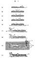
図1の(a)〜(i)は製造の工程を示している。
【0035】
図1は、自動車用エンジンコントロールユニットの構造と実装・成形方法を示す。多層セラミックの電子回路基板1は、長方形(60mm×65mm)で表面にSn/Ag系はんだペースト材2を印刷する(a)。この電子回路基板1にチップ抵抗体、セラミックコンデンサ、アルミコンデンサなどのチップ部品3(電子部品)を自動搭載機にて搭載後、その電子回路基板1を最高温度230〜250℃のリフロー炉内に通過してはんだ接合を行う(b)。
【0036】
この後、フラックスを除去するために、炭化水素系溶剤にて電子回路基板1を洗浄して所定温度のもとで、所定時間の乾燥を行なう。その後、デイスペンサを用いてAgペースト接着剤を所定の箇所に塗布し、電子部品としての半導体ベアチップ4(半導体チップ)を搭載する。150℃の温度で1時間かけ、Agペースト接着剤を硬化して半導体チップの電子回路基板への接合を完了する(c)。
【0037】
電子回路基板と半導体チップとの電気的接続を30μm径の金(Au)ワイヤ5を用いて超音波併用熱圧着方式で行う(d)。さらに、据え付け用の取り付け部分を有するアルミニウムなどの金属放熱板6(放熱用金属ベース)上に、上記の方法で部品搭載が済まされた電子回路基板を圧着した後、加熱硬化により接着(接着剤を介しての接着)を行なう(e)。次に熱可塑性樹脂のコネクタ7と金属放熱板6とをシリコーン系接着剤を用いて140℃/30分で同時接着させ一体化する(f)。ここで用いる接着剤としては、シリコーン接着剤の他に、ゴム微粒子配合の低弾性のエポキシ樹脂接着剤も用いることができる。コネクタ7の外部端子8(接続用金属端子)と電子回路基板との接続は線径300μmのアルミワイヤ9(接続線)を用いて室温で超音波方式による接合によって行う(g)。
【0038】
こうして作られたモジュールをトランスファモールド機に配置された175℃に加熱された金型10内に挿入後、エポキシ樹脂成形材料11を金型10内に圧入する。エポキシ樹脂成形材料11として、線膨張係数14ppm/℃、弾性率15Gpa、ガラス転移温度135℃の硬化後の物性を有し、かつ熱硬化する前の形態が室温(40℃以下)で固形の材料を用いる。成形圧力30kg/cm2で3分間の成形により熱硬化が行なわれる(h)。モジュールを金型から脱着させ(i)、150℃3時間の後硬化を行うが、必要に応じては、後硬化を省くこともできる。
【0039】
このようなモールド成形により、電子回路基板、電子部品、コネクタ7、ワイヤ5、アルミワイヤ9、金属放熱板6がエポキシ樹脂成形材料11による樹脂層で被覆された一体モールド構造のモジュールに出来上がるのである。
【0040】
上述したように熱硬化による樹脂層の成形は、短時間(3分間)で行なわれ、かつ成形用の金型内への樹脂成形材料の注入が圧力を加える押込みで行なわれる。このように樹脂層の成形時間が短かく、しかも樹脂成形材料の注入が簡単な押込みで出来るのは、熱硬化する前の形態が室温(40℃以下)で固形の材料を用いたことによるものである。ペースト状樹脂を用いた従来のものは、熱硬化に費やす成形時間が数十分であるので、本発明は成形時間が格段に短く、量産性に優れているのである。また従来のものは、成形用の金型内を高い真空状態にしないと、ペースト状樹脂が金型内に入らないので、特殊なコンプレッサーを必要とする。本発明は、そのような特殊なコンプレッサーが不要なので成形装置が複雑にならないのである。
【0041】
成形後のモジュールは、プログラム書き込み及び電気導通検査を経て、本発明の自動車エンジンコントロールユニットが得られる。なお、プログラム書き込みは、トランスファモールド成形前に行うこともできる。
【0042】
なお、本発明では、チップ部品(電子部品)の接合を、はんだの代わりにAgペースト接着剤を用いて行うことができる。この方法によれば、チップ部品と半導体ベアチップの電子回路基板上への搭載が一つの工程でできるため、工程数削減が可能となる。
【0043】
このコントロールユニットは、従来構造である図5のものとは違って樹脂ケースを必要としないため、小型で、かつ薄型となっていることが分かる。信頼性においても、従来構造と同等、またはそれ以上の特性を有することが確認されている。
【0044】
またコネクタ7の樹脂は、樹脂層の熱硬化温度よりも高い融点の熱可塑性樹脂を用いているので、樹脂層の熱硬化に際し、コネクタ7が融解して変形するようなことが生じない。変形がないので、コネクタ7へのコンセントの着脱に支障を来たさない。
【0045】
さらにコネクタ7の樹脂は熱可塑性樹脂を用いているので、熱硬化性樹脂とは違い外部端子8(接続用金属端子)との境界部分に成形バリが出来なく、コンセントの着脱に支障を来たさない。
【0046】
次に図2に示す第2の実施例について説明する。
【0047】
図2は、第2の実施例と同様な自動車用エンジンコントロールユニットの構造と実装・成形方法を示す。
【0048】
図2の(a)は電子部品と半導体チップを搭載した電子回路基板を示している。搭載の組み立て手順は、第1実施例の図1の(a)〜(e)と同じである。
【0049】
第1実施例との主なる違いは、半導体チップを予め、液状エポキシ樹脂で被覆して置くところである。
【0050】
さて、電子回路基板(セラミック)1上に搭載した半導体ベアチップ4のみを、線膨張係数13ppm/℃、弾性率13GPa、ガラス転位温度150℃の液状エポキシ樹脂12(熱硬化の樹脂)で封止後、100℃1時間+150℃1時間の条件で加熱硬化を行う(b)。この熱硬化の樹脂層は、後述する樹脂層の下になる下樹脂層で第一絶縁層と言う。
【0051】
その後、アルミニウムなどの金属放熱板6(放熱用金属ベース)上に、上記の方法で電子部品を搭載した電子回路基板を圧着した後、加熱硬化により接着(接着剤を介しての接着)する(c)。
【0052】
次に樹脂のコネクタ7と金属放熱板6とを低弾性のエポキシ系接着剤を用いて150℃60分で同時接着させ一体化する(d)。次に、樹脂のコネクタの外部端子8(接続用金属端子)と電子回路基板との接続は線径300μmのアルミワイヤ9(接続線)を用いて室温で超音波方式による接合によって行う(e)。最終的に、このモジュールを実施例1と同じエポキシ樹脂成形材料11と成形条件を用いてトランスファモールドを行うことによって、本発明の自動車エンジンコントロールユニットを得る(f)。エポキシ樹脂成形材料1による樹脂層で被覆された一体モールド構造のモジュールに出来上がるのである。
【0053】
こうして得られたコントロールユニットは、第1の実施例と同様に小型、薄型となっている。信頼性も実施例1で得られたユニットよりも優れていることを確認している。
【0054】
なお、エポキシ樹脂成形材料1による熱硬化の樹脂層を第二絶縁層と言う。この第二絶縁層と第一絶縁層による二重の絶縁層で半導体チップのところが被覆されている。半導体チップのワイヤボンデング部分が液状の第一絶縁層で先に封止され、第二絶縁層(エポキシ樹脂層)からの応力が緩和される。これにより、ワイヤボンデングの断線や変形が抑制され、信頼性も実施例1で得られたユニットよりも優れていることを確認している。
【0055】
次に図3に示す第3の実施例について説明する。
【0056】
図3は、電子回路基板として樹脂プリントの電子回路基板を用いたセンサーコントロールユニットの構造と実装並びに成形方法を示す。
【0057】
図3において、ガラス転位温度130℃、線膨張係数15ppm/℃の物性を有する(80×35)mmの2層樹プリントの電子回路基板13の片面上にSn/Pb共晶はんだペースト材2を印刷する(a)。この電子回路基板に、チップ抵抗体、セラミックコンデンサ、アルミコンデンサなどのチップ部品3(電子部品)と半導体パッケージ14を自動搭載機にて搭載後、電子回路基板を最高温度(210〜240)℃のリフロー炉内に通過してはんだ接合を行う(b)。フラックスを除去するために、炭化水素系溶剤にて電子回路基板を洗浄して所定温度、時間で乾燥する。ここで、無洗浄用の半田フラックスを用いる場合は、電子部品搭載後の洗浄工程を省くことができる。その後、ピン挿入型電子部品と樹脂のコネクタ7の端子リードを電子回路基板のスルーホールに挿入後、電子回路基板の裏面をフロー半田にて電子回路基板との接合を完了する(c)。このモジュールをトランスファモールド機に配置された165℃の金型10内に挿入後、線膨張係数15ppm/℃、弾性率13Gpa、ガラス転移温度155℃の硬化後の物性を有する室温で固形のエポキシ樹脂成形材料11を用いて、成形圧力30kg/cm2において3分間で成形を行う(d)。モジュールを金型から脱着させた後(e)、プログラム書き込み及び電気導通検査を経て、本発明の自動車センサーコントロールユニットを得る。
【0058】
こうして得られたセンサーコントロールユニットは、従来構造である図7と比べて、樹脂ケースが省略できるため、小型で、かつ薄型となっていることが分かる。信頼性においても−40℃〜130℃の熱衝撃試験において2000サイクル以上、85℃85%の高温高湿試験において2000時間以上でも、正常な動作を示すという優れた特性を有する。
【0059】
次に図4に示す第4の実施例について説明する。
【0060】
図4は、本発明による自動車用圧力センサーの構造と実装、成形方法を示す。
【0061】
図4において、ガラス台15の上にセンサーチップ16をダイヤフラム17が下向きになるようにして配置し、両者を真空中で接合温度450℃、印加電圧400V,電圧印加時間300秒の条件の元に陽極接合によって気密接合する(a)。この組み品を外部リード19と開口部を有する樹脂ケース材上18にシリコーン系接着剤を用いて接着させる(b)。接着材の硬化条件は140℃、30分である。次に、センサーチップ16と外部リード19をワイヤ9を用いて超音波併用熱圧着方式により、ボンデイング接合する(c)。その後、シリコーンゲル20を用いてガラス台15、センサーチップ16及びアルミなどの金属ワイヤ9を覆うようにして塗布し(d)、140℃30分の条件で硬化を行って、半導体圧力センサーユニット21を得る。次に、測定圧力の導圧孔22、コネクタ取り付け部、及び前記コネクタ受け部の中に突出した端子8を有するエンジン取り付け用樹脂ケースの中に、前記半導体圧力センサーユニットを、図4(e)に示したように圧力センサーユニットの加圧面が導圧孔22と向かい合うように配置し、この位置で樹脂ケース板40から引き出した外部リード19とコネクタ端子8との間を金属ワイヤ9を用いてボンデイング接合して樹脂の電子回路基板を有するセンサー組立体を得る。さらに、このセンサー組立体を、トランスファモールド機内の金型10内に装着した後、導圧孔に通じる樹脂ケースの開放面を除いて、樹脂ケースの外周と外ケースとの間の隙間をエポキシ樹脂成形材料11で充填、封止する{(f)、(g)}。この時に使用するエポキシ樹脂成形材料の硬化後の物性は線膨張係数が12ppm/℃、弾性率が20GPa、ガラス転位温度が120℃である。成形条件としては、成形圧力が20kg/cm2、成形温度175℃、成形時間が90秒である。得られた圧力センサーは、キャップ無しでも気密性の高い製品となるばかりではなく、短時間に成形できるため生産性にも優れる。
【0062】
上記実施例で述べた発明の良さをまとめて説明する。
【0063】
電子部品と電子回路基板の封止、コネクタとの接着、及び電気・電子モジュール全体の構造体の成形が1種類のエポキシ樹脂成形材料で同時にできるため、従来から用いていた樹脂ケース、キャップ、シリコーンゲルなどが不要となり、部品点数の削減と工数低減に効果がある。樹脂ケースやキャップの省略、及び封止面積の最少化は、モジュールの小型、薄型化を図る上で効果が大きい。また、エポキシ樹脂成形材料(熱硬化樹脂)は室温で固形であるため、取り扱いが容易である。しかも、室温で固形である熱硬化樹脂は、室温でペースト状の熱硬化樹脂とは違い、トランスファモールド成形法やコンプレッション成形法によって加熱加圧で短時間成形できるため、既存の安価な生産設備を活用できるとともに、作業時間の大幅な短縮が可能である。それに加え、成形用の金型内を高い真空状態にしなくとも樹脂の注入が出来るので、特殊なコンプレッサーを必要とせず、生産設備が安価になる。本発明で用いるエポキシ樹脂成形材料は従来の半導体封止材料と同じ樹脂物性を有するため、低熱膨張性、低吸湿性、及び高接着性であり、成形後の電気・電子モジュールの高信頼性化を図ることができる。また、金型を用いた加圧成形法であるため、製品の外形形状の自由化が可能であり、しかも優れた外観を得ることができるという効果がある。
【0064】
【発明の効果】
以上述べたように本発明によれば、樹脂の熱硬化時間が早くて量産性に優れ、かつ高真空に保たなくとも樹脂注入ができる電子部品の一体モールド構造を有する電気・電子モジュールを提供できる。
【図面の簡単な説明】
【図1】本発明の実施例に係わるもので、自動車用エンジンコントロールユニットの構造と実装・成形方法を示す断面図。
【図2】本発明の別の実施例に係わるもので、自動車用エンジンコントロールユニットの構造と実装・成形方法を示す断面図。
【図3】本発明の別の実施例に係わるもので、回路基板として樹脂プリント基板を用いたセンサーコントロールユニットの構造と実装並びに成形方法を示す断面図。
【図4】本発明の別の実施例に係わるもので、自動車用圧力センサーの構造と実装、成形方法を示す断面図。
【図5】従来の自動車用エンジンコントロールユニットの構造を示す断面図。
【図6】従来のパワー半導体モジュールの構造を示す断面図。
【図7】従来の自動車または民生用で採用されている電子回路装置の構造を示す断面図。
【図8】従来の圧力センサーモジュールの構造を示す断面図。
【図9】従来の電子回路基板とコネクタとを一体的に結合する樹脂形成タイプの電子回路装置の構造と成形方法を示す断面図。
【符号の説明】
1…セラミックの電子回路基板、2…はんだペースト材、3…チップ部品、4…半導体ベアチップ、5…Auワイヤ、6…金属放熱板、7…樹脂のコネクタ、8…コネクタ端子リード、9…アルミワイヤ、10…金型、11…室温で固形のエポキシ成形材料、12…液状エポキシ樹脂、13…樹脂の電子回路基板、14…半導体パッケージ、15…ガラス台、16…センサーチップ、17…ダイヤフラム、40…樹脂ケース板、19…外部リード、20…シリコーンゲル、21…半導体圧力センサーユニット、22…導圧孔、23…キャップ、24…パワー半導体素子、25…制御用集積回路素子、26…封止または保護樹脂、27…空気排出路。[0001]
BACKGROUND OF THE INVENTION
The present invention includes a connector having at least a metal terminal for connection, an electronic component mounted on a ceramic, organic resin, or resin printed electronic circuit board, a resin for sealing the electronic component, and the electronic circuit board and the connector. An electrical / electronic module composed of a metal lead or a connecting wire such as a wire or a flexible conductor is integrally formed using a resin molding material having low thermal expansion and low moisture absorption, and at least the board of the connector The present invention relates to a low-cost and high-reliability electric / electronic module that can be achieved by simultaneously sealing the connecting surface side and the electronic component, and a molding method thereof.
[0002]
[Prior art]
Various control units and sensor modules of automobiles have a structure composed of a ceramic or resin electronic circuit board on which an electronic circuit is mounted, a metal or plastic case having an input / output connector portion, and / or a cap. These structures include a structure in which the above-described ceramic or resin electronic circuit board is mounted on a metal base for heat dissipation in order to improve the heat dissipation of the semiconductor chip.
[0003]
As an example of a conventional control unit, FIG. 5 shows the structure of an engine control unit using a ceramic electronic circuit board.
[0004]
6 and 7 show a conventional resin molding type electronic circuit device. FIG. 6 shows a structure adopted in a semiconductor power module or the like as described in JP-A-9-45851 and JP-A-2001-326303. The electronic component (
[0005]
On the other hand, FIG. 7 shows a structure of an electronic circuit device adopted for automobiles or consumer use. A
[0006]
FIG. 8 shows the structure of the pressure sensor module described in Japanese Patent No. 3149678. The
[0007]
[Problems to be solved by the invention]
As shown above, the conventional structure is an electronic circuit board on which electronic components are mounted, a connector having a metal terminal for connection electrically connected to the electronic circuit board, a case for storing the electronic circuit board, silicone gel and epoxy. Having a protective resin such as resin and / or a cap has the following problems.
[0008]
From the viewpoint of improving the comfort of automobiles, the engine room tends to be narrower and the cabin space tends to be wider. As a result, the control unit has been required to be smaller and thinner, but the conventional structure is a structure that houses the electronic circuit board in the case, so the module tends to be larger and thicker. Can no longer satisfy this requirement.
[0009]
In order to remedy this problem, a resin-forming type electronic circuit device for integrally connecting an electronic circuit board and a connector as shown in FIG. 9A is described in Japanese Patent Laid-Open No. 7-22722. . As shown in FIG. 9B, this publication proposes a low-pressure molding method in which a paste-like resin is poured into a mold kept in a vacuum state and then heat-cured as a method for forming a protective resin.
[0010]
However, this method requires a special mold structure and apparatus for maintaining a vacuum state, and since a paste-like resin is used as a protective resin, the curing time becomes several tens of minutes and the product is taken out of the mold. Longer time is a problem.
[0011]
Furthermore, the protective resin combined with the thermal expansion coefficient of the electronic circuit board and the electronic component has a very high paste-like resin viscosity before curing, so a high vacuum is required for resin injection, and the productivity is poor. .
[0012]
Further, in an electronic circuit device in which an electronic circuit board or an electronic circuit is mounted on a heat radiating metal plate, it is difficult to position the connector or the heat radiating metal plate, so that the vacuum / low pressure forming method is substantially difficult. Further, even in a pressure sensor having a pressure introduction hole for pressure measurement, since a vacuum state is maintained from the point of the sensor shape, the mold structure is complicated, and positioning of the outer case of the sensor becomes difficult.
[0013]
The present invention has been made in view of the above points, and the heat curing time of a resin as a protective layer (resin layer) covering an electronic circuit board or an electronic component is fast, excellent in mass productivity, and high in vacuum. It is an object of the present invention to provide an electric / electronic module having an integral mold structure of electronic parts that can be injected with resin without being kept.
[0014]
Further, the present invention provides a resin molding material having low thermal expansion, low hygroscopicity, and high adhesiveness in order to improve the reliability of electronic circuit devices, reduce the size and weight, and reduce the number of members and man-hours. The present invention provides an electrical / electronic module that performs integral molding under heat and pressure and simultaneously seals a circuit board on which electronic components are mounted and at least a connection surface side of the connector with the board, and a molding method thereof. is there.
[0015]
[Means for Solving the Problems]
The present invention relates to an electric / electronic module having an integrated structure of an electronic component including a connector, an electronic component, and a thermosetting resin layer covering an electronic circuit board, wherein the resin of the resin layer is before thermosetting. Is a solid at a temperature of 40 ° C. or lower.
[0016]
More specifically,
[0017]
In the present invention, the electronic component mounted on the electronic circuit board and the connection of at least the metal lead, the wire, the flexible connection conductor, etc., arranged on the attachment part side (connection surface side) where the connector is attached to the electronic circuit board The resin used for sealing so as to completely cover the wire is a solid epoxy resin molding material containing an inorganic filler at 40 ° C. or lower, and is a normal sealing for resin-sealed semiconductor devices The same material can be used. This solid epoxy resin molding material is the most suitable sealing resin for integral molding under heat and pressure, and can simultaneously ensure moldability and reliability of the electric / electronic module.
[0018]
Furthermore, this epoxy resin molding material (thermosetting resin) has excellent adhesion to connectors made of thermoplastic resin made of polybutylene terephthalate, nylon, or polyphenylene sulfide, and is a metal lead that is a concern in durability tests, Since there is no disconnection or peeling of the connection lines such as wires and flexible connection conductors (detachment of the resin from the electronic circuit board, electronic components, connection lines, connectors, etc.), there is a great effect in improving the reliability. One of the reasons why the adhesion is improved is that the molding temperature is 150 to 180 ° C., and therefore, the interface between the connector resin and the epoxy resin causes molecular entanglement to form a strong adhesive interface. Can be mentioned. As the inorganic filler contained in the epoxy resin molding material, at least one of crushed or spherical shapes such as fused silica, crystalline silica, alumina, and magnesium oxide can be used. The epoxy resin molding material is composed of an epoxy resin and a phenol resin curing agent, and is an orthocresol type epoxy resin that is solid at 40 ° C. or lower, an epoxy resin having a biphenyl skeleton, an epoxy resin having a dicyclopentadiene skeleton, and naphthalene. It can be obtained from a combination of an epoxy resin having a skeleton or a bisphenol A type epoxy resin and a phenol novolac resin, an orthocresol novolak resin, a phenol resin having a dicyclopentadiene skeleton, or a phenol resin having a naphthalene skeleton. In addition, the epoxy resin molding material can contain a stress-reducing material such as silicone rubber or oil or butadiene rubber in order to reduce the stress by reducing the elastic modulus.
[0019]
In the present invention, an electronic component mounted on an electronic circuit board and a connection line such as a metal lead, a wire, a flexible connection conductor, etc., which are arranged at least on the attachment part side (connection surface side) where the connector is attached to the electronic circuit board As a sealing resin, the physical properties of the cured resin
Linear expansion coefficient: (8-25) × 10- 6/ ℃,
Elastic modulus; (8-25) GPa,
Glass transition temperature; (80-160) ° C.,
It is characterized by being.
[0020]
These resin properties are due to the stress caused by the difference due to the linear expansion coefficient of the electronic component, electronic circuit board, and heat dissipation metal plate (heat dissipation metal base), or to the joint part by soldering the electronic component to the electronic circuit board. Since the coefficient of linear expansion needs to be as close as possible to these members, (8-25) × 10 in the present invention.- 6/ C.
[0021]
In addition, since the electrical / electronic module of the present invention uses electronic parts and various members having different linear expansion coefficients, in order to reduce the stress, in addition to defining the linear expansion coefficient, it is preferable to reduce the elastic modulus. In order to ensure mold releasability, the elastic modulus is in the range of (8-25) GPa. The glass transition temperature is also preferably low from the viewpoint of low stress, but (80 to 160) ° C. is preferable from the viewpoint of mold releasability during molding and heat resistance of the module.
[0022]
In the present invention, as an automobile engine control unit or an automobile sensor electric / electronic module that can be mounted in or on an automobile engine, at least a connector having a metal terminal for connection, a ceramic electronic circuit boardBoardIn addition, the electronic properties mounted on the electronic circuit board, and metal leads for electrically connecting the electronic circuit board and the connector, wires, flexible connection conductors, etc., the cured resin physical properties,
Linear expansion coefficient: (8-25) × 10- 6/ ℃,
Elastic modulus; (8-25) GPa,
Glass transition temperature; (80-160) ° C.,
It is characterized by having a structure in which a connector and an electronic component are integrally molded under heat and pressure using a resin in the range of.
[0023]
In addition, this module may include a structure having a heat radiating metal base such as aluminum, copper, or iron (including those plated on the surface) in order to improve heat dissipation. On this heat radiating metal base, an electronic circuit board on which electronic parts are mounted is bonded using an adhesive such as silicone resin, epoxy resin, or acrylic resin.
[0024]
Furthermore, in the module of the present invention in which a ceramic material is used as an electronic circuit board and the semiconductor bare chip is electrically bonded by gold wire wire bonding or solder bump, only the semiconductor chip portion mounted on the ceramic electronic circuit board is sealed. A hard first insulating layer to be stopped, and an epoxy resin insulating layer for simultaneously sealing the mounting portion side (connection surface side) and the electronic component to be attached to the electronic circuit board as a second resin insulating layer on the first insulating layer It is characterized by forming.
[0025]
The hard first insulating layer is provided in order not to directly transmit stress generated by a slight difference in expansion coefficient between the sealing resin and the ceramic electronic circuit board to the semiconductor bare chip (semiconductor chip). The resin forming the first insulating layer has a linear expansion coefficient in the range of (8 to 20) ppm / ° C., which is close to the linear expansion coefficient of the ceramic electronic circuit board and the semiconductor chip, and has an elastic modulus of (1 to 20) An epoxy resin, a polyamideimide resin, or a polyamideimide resin having an epoxy resin in the range of GPa is suitable.
[0026]
Although the formation of the first insulating layer with low elastic silicone rubber or silicone gel is effective for low stress, it is preferable not to use it in the present invention for the following reason. That is, in the formation of the second resin insulating layer by the heat and pressure molding method, deformation, disconnection, and peeling of the gold wire bonding portion or the solder bump bonding portion occur due to deformation of the insulating layer due to pressure.
[0027]
In the present invention, a connector having at least a metal terminal for connection, a resin electronic circuit board, an electronic component mounted on the electronic circuit board, and a metal lead and a wire for electrically connecting the electronic circuit board and the connector The physical properties of the resin after curing the automotive control unit with connection wires such as flexible connection conductors,
Linear expansion coefficient: (8-25) × 10- 6/ ℃,
Elastic modulus; (8-25) GPa,
Glass transition temperature; (80-160) ° C.,
The connector and the electronic component can be integrally molded under heat and pressure using a resin in the range of. The linear expansion coefficient, the elastic modulus, and the glass transition temperature of the resin are preferably in the above ranges, but among these, the linear expansion coefficient is particularly the linear expansion coefficient of the resin electronic circuit board (15 to 17 ppm). (10 to 20) ppm / ° C. is preferable because the stress can be further reduced.
[0028]
In the present invention, the integral mold structure of the connector and the electronic component is molded by using a low-pressure transfer molding machine or a compression molding machine in a molding pressure range of (5-70) kg /
[0029]
That is, in order to prevent deformation of the connector at the time of molding, low pressure molding of 70 kg /
[0030]
In the above structure, the epoxy resin molding material that integrally molds the electronic component and the connector has the same cured material properties as the sealing material used for the resin-encapsulated semiconductor device, and has low thermal expansion, Since it has low hygroscopicity and high adhesiveness and low ionic impurities, the reliability of the electric / electronic module can be improved. In particular, a material close to the linear expansion coefficient of an electronic component or an electronic circuit board can be freely selected, which is effective in improving reliability. Moreover, since the said epoxy resin molding material is excellent also in adhesiveness with the connector of resin, there exists a big effect also with respect to the reliability improvement of a module. In addition, metal wires and solder joints for electronic parts and connections and joints are fixed by sealing with an epoxy resin molding material, providing excellent vibration resistance and joint fatigue resistance during temperature cycling or thermal shock testing. Have.
[0031]
In the present invention, since the epoxy resin molding material is heat-press molded by a transfer molding method or a compression method using a mold, productivity is higher than when a liquid resin is used. Further, since the outer shape of the module can be determined by the shape of the mold, the module can be easily reduced in size and thickness as compared with the case where the case material is used.
[0032]
DETAILED DESCRIPTION OF THE INVENTION
Embodiments of the present invention will be described below with reference to the drawings.
[0033]
First, a first embodiment will be described with reference to FIG.
[0034]
(A)-(i) of FIG. 1 has shown the process of manufacture.
[0035]
FIG. 1 shows the structure and mounting / molding method of an automobile engine control unit. The multilayer ceramic
[0036]
Thereafter, in order to remove the flux, the
[0037]
Electrical connection between the electronic circuit board and the semiconductor chip is performed by a ultrasonic thermocompression bonding method using a gold (Au)
[0038]
After the module thus produced is inserted into a
[0039]
By such molding, an electronic circuit board, an electronic component, a
[0040]
As described above, the molding of the resin layer by thermosetting is performed in a short time (3 minutes), and the injection of the resin molding material into the molding die is performed by pressing to apply pressure. The reason why the molding time of the resin layer is short and the injection of the resin molding material can be performed by simple pressing is that the form before thermosetting is a solid material at room temperature (40 ° C or lower). It is. In the conventional one using a paste-like resin, the molding time spent for thermosetting is several tens of minutes. Therefore, the molding time is remarkably short and the mass productivity is excellent. Further, the conventional one requires a special compressor because the paste-like resin does not enter the mold unless the molding mold is brought into a high vacuum state. Since the present invention does not require such a special compressor, the molding apparatus is not complicated.
[0041]
The molded module is subjected to program writing and electrical continuity inspection to obtain the automobile engine control unit of the present invention. The program writing can also be performed before transfer molding.
[0042]
In the present invention, chip parts (electronic parts) can be joined using an Ag paste adhesive instead of solder. According to this method, since the chip component and the semiconductor bare chip can be mounted on the electronic circuit board in one process, the number of processes can be reduced.
[0043]
Unlike the conventional structure of FIG. 5, this control unit does not require a resin case, so that it can be seen that it is small and thin. In terms of reliability, it has been confirmed that it has characteristics equal to or higher than those of conventional structures.
[0044]
Moreover, since the resin of the
[0045]
Further, since the resin of the
[0046]
Next, a second embodiment shown in FIG. 2 will be described.
[0047]
FIG. 2 shows the structure and mounting / molding method of an automobile engine control unit similar to that of the second embodiment.
[0048]
FIG. 2A shows an electronic circuit board on which an electronic component and a semiconductor chip are mounted. The assembly procedure of mounting is the same as (a) to (e) of FIG. 1 of the first embodiment.
[0049]
The main difference from the first embodiment is that a semiconductor chip is previously coated with a liquid epoxy resin.
[0050]
Now, after sealing only the semiconductor
[0051]
Thereafter, the electronic circuit board on which the electronic component is mounted is crimped on the metal heat radiating plate 6 (heat radiating metal base) such as aluminum, and then bonded by heat curing (adhesion via an adhesive) ( c).
[0052]
Next, the
[0053]
The control unit thus obtained is small and thin as in the first embodiment. It has been confirmed that the reliability is superior to the unit obtained in Example 1.
[0054]
The thermosetting resin layer made of the epoxy
[0055]
Next, a third embodiment shown in FIG. 3 will be described.
[0056]
FIG. 3 shows the structure, mounting and molding method of a sensor control unit using a resin printed electronic circuit board as the electronic circuit board.
[0057]
In FIG. 3, the Sn / Pb eutectic
[0058]
It can be seen that the sensor control unit thus obtained is smaller and thinner than the conventional structure of FIG. 7 because the resin case can be omitted. In terms of reliability, it has an excellent characteristic that it exhibits normal operation even in a thermal shock test of -40 ° C to 130 ° C for 2000 cycles or more and in a high temperature and high humidity test of 85 ° C and 85% for 2000 hours or more.
[0059]
Next, a fourth embodiment shown in FIG. 4 will be described.
[0060]
FIG. 4 shows the structure, mounting, and molding method of an automotive pressure sensor according to the present invention.
[0061]
In FIG. 4, the
[0062]
The advantages of the invention described in the above embodiment will be described together.
[0063]
Sealing electronic components and electronic circuit boards, bonding connectors, and forming the entire structure of electrical and electronic modules at the same time with a single epoxy resin molding material. There is no need for gel etc., which is effective in reducing the number of parts and man-hours. The omission of the resin case and the cap and the minimization of the sealing area are very effective in reducing the size and thickness of the module. Moreover, since the epoxy resin molding material (thermosetting resin) is solid at room temperature, it is easy to handle. Moreover, unlike thermosetting resins that are solid at room temperature, thermosetting resins that are solid at room temperature can be molded in a short time by heat and pressure using the transfer molding method or compression molding method. It can be used and the working time can be greatly reduced. In addition, since the resin can be injected without making the inside of the molding die into a high vacuum state, a special compressor is not required, and the production equipment is inexpensive. The epoxy resin molding material used in the present invention has the same resin physical properties as a conventional semiconductor sealing material, so it has low thermal expansion, low moisture absorption, and high adhesion, and high reliability of the electric / electronic module after molding. Can be achieved. In addition, since it is a pressure molding method using a mold, it is possible to liberalize the outer shape of the product and to obtain an excellent appearance.
[0064]
【The invention's effect】
As described above, according to the present invention, there is provided an electric / electronic module having an integral mold structure of an electronic component capable of injecting the resin without being kept at a high vacuum, with a fast resin thermosetting time and excellent mass productivity. it can.
[Brief description of the drawings]
FIG. 1 is a cross-sectional view showing a structure of an automobile engine control unit and a mounting / molding method according to an embodiment of the present invention.
FIG. 2 is a cross-sectional view showing the structure and mounting / molding method of an automobile engine control unit according to another embodiment of the present invention.
FIG. 3 is a sectional view showing the structure, mounting and molding method of a sensor control unit using a resin printed board as a circuit board according to another embodiment of the present invention.
FIG. 4 is a cross-sectional view showing the structure, mounting, and molding method of an automotive pressure sensor according to another embodiment of the present invention.
FIG. 5 is a cross-sectional view showing the structure of a conventional automobile engine control unit.
FIG. 6 is a cross-sectional view showing the structure of a conventional power semiconductor module.
FIG. 7 is a cross-sectional view showing a structure of an electronic circuit device employed in a conventional automobile or consumer use.
FIG. 8 is a cross-sectional view showing the structure of a conventional pressure sensor module.
FIG. 9 is a cross-sectional view showing a structure and a molding method of a resin-forming type electronic circuit device that integrally couples a conventional electronic circuit board and a connector.
[Explanation of symbols]
DESCRIPTION OF
Claims (14)
前記樹脂層の樹脂は、熱硬化前の形態が40℃以下の温度において固形であることを特徴とする電子部品の一体モールド構造を有する電気・電子モジュール。An electronic circuit board formed of ceramic or resin, an electronic component mounted on the electronic circuit board, and a connecting metal connected to the electronic circuit of the electronic circuit board and detachably connected to an external electronic circuit system There is provided an electric / electronic module having an integral molding structure of electronic components including a connector formed of a resin having terminals and a thermosetting resin layer covering the connector, the electronic component, and the electronic circuit board. And
The electric / electronic module having an integral mold structure for electronic parts, wherein the resin of the resin layer is solid at a temperature of 40 ° C. or lower before thermosetting.
前記コネクタの樹脂は、前記樹脂層の熱硬化温度よりも高い融点の熱可塑性樹脂とし、
前記樹脂層の樹脂は、熱硬化前の形態が40℃以下の温度において固形であることを特徴とする電子部品の一体モールド構造を有する電気・電子モジュール。An electronic circuit board formed of ceramic or resin, an electronic component mounted on the electronic circuit board, and connected to an electronic circuit of the electronic circuit board via a connection line and detachably connected to an external electronic circuit system A connector formed of a resin having a connecting metal terminal, and a thermosetting resin layer covering the connector, the connecting wire, the electronic component, and the electronic circuit board. In an electric / electronic module having an integral mold structure,
The resin of the connector is a thermoplastic resin having a melting point higher than the thermosetting temperature of the resin layer,
The electric / electronic module having an integral mold structure for electronic parts, wherein the resin of the resin layer is solid at a temperature of 40 ° C. or lower before thermosetting.
前記樹脂層の樹脂は、無機質フィラを含むエポキシ樹脂であることを特徴とする電子部品の一体モールド構造を有する電気・電子モジュール。An electric / electronic module having an integral mold structure for an electronic component according to claim 1 or 2,
The resin of the resin layer is an epoxy resin containing an inorganic filler, The electric / electronic module having an integral mold structure of electronic parts,
前記樹脂層の樹脂は、熱硬化後の物性が、
線膨張係数;(8〜25)×10― 6/℃、
弾性率;(8〜25)GPa、
ガラス転移温度;(80〜160)℃、
の範囲にあることを特徴とする電子部品の一体モールド構造を有する電気・電子モジュール。In the electric / electronic module which has the integral mold structure of the electronic component as described in any one of Claims 1-3,
The resin of the resin layer has physical properties after thermosetting,
Coefficient of linear expansion; (8~25) × 10 - 6 / ℃,
Elastic modulus; (8-25) GPa,
Glass transition temperature; (80-160) ° C.,
An electric / electronic module having an integral mold structure for electronic parts, characterized in that it is in the range of
前記電子回路基板に装着する放熱用金属ベースを有することを特徴とする電子部品の一体モールド構造を有する電気・電子モジュール。An electric / electronic module having an integral mold structure for electronic components according to claim 5,
An electric / electronic module having an integral molding structure of electronic parts, comprising a metal base for heat dissipation to be mounted on the electronic circuit board.
前記放熱用金属ベースは、前記電子部品の非装着面側に装着することを特徴とする電子部品の一体モールド構造を有する電気・電子モジュール。An electric / electronic module having an integral mold structure for an electronic component according to claim 6,
The heat-dissipating metal base is mounted on the non-mounting surface side of the electronic component.
前記放熱用金属ベースは、接着剤を介して装着したことを特徴とする電子部品の一体モールド構造を有する電気・電子モジュール。An electric / electronic module having an integral mold structure for an electronic component according to claim 6,
An electric / electronic module having an integral mold structure of electronic parts, wherein the heat dissipating metal base is mounted via an adhesive.
前記放熱用金属ベースは、少なくとも前記電子回路基板に対向する面側が前記熱硬化性の樹脂層で被われることを特徴とする電子部品の一体モールド構造を有する電気・電子モジュール。An electric / electronic module having an integral mold structure for an electronic component according to claim 6,
The electric / electronic module having an integral mold structure for electronic parts, wherein the heat dissipating metal base is covered with the thermosetting resin layer at least on the side facing the electronic circuit board.
前記電子部品の半導体チップについては、前記熱硬化性の樹脂層で被覆する前に予め下樹脂層の被覆を施し、該下樹脂層を第1絶縁層とし、第一絶縁層の上側になる前記熱硬化性の樹脂層を第二絶縁層とし、半導体チップのところが二重の絶縁層で被覆されていることを特徴とする電子部品の一体モールド構造を有する電気・電子モジュール。In the electric / electronic module having an integral mold structure of the electronic component according to any one of claims 1 to 9,
For the semiconductor chip of the electronic component, the lower resin layer is coated in advance before coating with the thermosetting resin layer, the lower resin layer is used as the first insulating layer, and the upper side of the first insulating layer. An electric / electronic module having an integrated structure of electronic parts, wherein a thermosetting resin layer is a second insulating layer, and a semiconductor chip is covered with a double insulating layer.
前記接続線は、前記樹脂層で全体的に被覆され、前記コネクタは前記接続線に接続される接続側が前記樹脂層で被覆され、
前記樹脂層の樹脂は、熱硬化後の物性が、
線膨張係数;(8〜25)×10― 6/℃、
弾性率;(8〜25)GPa、
ガラス転移温度;(80〜160)℃、
の範囲にあることを特徴とする電子部品の一体モールド構造を有する電気・電子モジュール。An electronic circuit board formed of ceramic or resin, an electronic component mounted on the electronic circuit board, and connected to an electronic circuit of the electronic circuit board via a connection line and detachably connected to an external electronic circuit system A connector formed of a resin having a connecting metal terminal, and a thermosetting resin layer covering the connector, the connecting wire, the electronic component, and the electronic circuit board. In an electric / electronic module having an integral mold structure,
The connection line is entirely covered with the resin layer, and the connector is covered with the resin layer on the connection side connected to the connection line,
The resin of the resin layer has physical properties after thermosetting,
Coefficient of linear expansion; (8~25) × 10 - 6 / ℃,
Elastic modulus; (8-25) GPa,
Glass transition temperature; (80-160) ° C.,
An electric / electronic module having an integral mold structure for electronic parts, characterized in that it is in the range of
前記樹脂層の樹脂として、熱硬化前の形態が40℃以下の温度において固形である樹脂を用い、
成形圧力が(5〜70)kg/cm2、成形温度が(150〜180)℃の範囲で低圧トランスファモールド成形機またはコンプレッション成形機によりモールド成形することを特徴とする電子部品の一体モールド構造を有する電気・電子モジュールの成形方法。An electronic circuit board formed of ceramic or resin, an electronic component mounted on the electronic circuit board, and a connecting metal connected to the electronic circuit of the electronic circuit board and detachably connected to an external electronic circuit system Molding of an electric / electronic module having an integral molding structure of an electronic component including a connector formed of a resin having terminals, and a thermosetting resin layer covering the connector, the electronic component, and the electronic circuit board In the way,
As the resin of the resin layer, a resin whose form before thermosetting is solid at a temperature of 40 ° C. or lower is used.
An electronic component integrated molding structure characterized by molding with a low pressure transfer molding machine or a compression molding machine within a molding pressure range of (5-70) kg / cm 2 and a molding temperature range of (150-180) ° C. Molding method of electric / electronic module.
該電気・電子モジュールが自動車用エンジンコントロールユニットまたは自動車センサー用であることを特徴とする電子部品の一体モールド構造を有する電気・電子モジュールの成形方法。A method for forming an electric / electronic module having an integral mold structure for an electronic component described in claim 7,
A method for forming an electric / electronic module having an integral molding structure of electronic parts, wherein the electric / electronic module is for an automobile engine control unit or an automobile sensor.
電子回路基板として、樹脂プリント電子回路基板を用いたことを特徴とする電子部品の一体モールド構造を有する電気・電子モジュールの成形方法。In any one statement of Claims 1-11,
A method for forming an electric / electronic module having an integral molding structure of electronic parts, wherein a resin printed electronic circuit board is used as the electronic circuit board.
Priority Applications (1)
| Application Number | Priority Date | Filing Date | Title |
|---|---|---|---|
| JP2002268201A JP3884354B2 (en) | 2002-09-13 | 2002-09-13 | Electrical / electronic module with integrated molded structure of connector and electronic component |
Applications Claiming Priority (1)
| Application Number | Priority Date | Filing Date | Title |
|---|---|---|---|
| JP2002268201A JP3884354B2 (en) | 2002-09-13 | 2002-09-13 | Electrical / electronic module with integrated molded structure of connector and electronic component |
Publications (2)
| Publication Number | Publication Date |
|---|---|
| JP2004111435A true JP2004111435A (en) | 2004-04-08 |
| JP3884354B2 JP3884354B2 (en) | 2007-02-21 |
Family
ID=32266483
Family Applications (1)
| Application Number | Title | Priority Date | Filing Date |
|---|---|---|---|
| JP2002268201A Expired - Lifetime JP3884354B2 (en) | 2002-09-13 | 2002-09-13 | Electrical / electronic module with integrated molded structure of connector and electronic component |
Country Status (1)
| Country | Link |
|---|---|
| JP (1) | JP3884354B2 (en) |
Cited By (37)
| Publication number | Priority date | Publication date | Assignee | Title |
|---|---|---|---|---|
| EP1646271A2 (en) | 2004-10-06 | 2006-04-12 | Hitachi, Ltd. | Control device and method of manufacturing thereof |
| EP1677583A1 (en) * | 2005-01-04 | 2006-07-05 | Hitachi, Ltd. | Electronic control unit and method thereof |
| JP2006190725A (en) * | 2005-01-04 | 2006-07-20 | Hitachi Ltd | Resin-sealing engine controller and its manufacturing method |
| JP2006303327A (en) * | 2005-04-22 | 2006-11-02 | Denso Corp | Electronic circuit device and its manufacturing method |
| JP2006303106A (en) * | 2005-04-19 | 2006-11-02 | Denso Corp | Electronic circuit device |
| JP2007095933A (en) * | 2005-09-28 | 2007-04-12 | Showa Denko Kk | Solid electrolytic capacitor and manufacturing method thereof |
| JP2007180160A (en) * | 2005-12-27 | 2007-07-12 | Showa Denko Kk | Capacitor chip and manufacturing method thereof |
| JP2007273796A (en) * | 2006-03-31 | 2007-10-18 | Hitachi Ltd | Electric electronic module of car |
| JP2007288701A (en) * | 2006-04-20 | 2007-11-01 | Hitachi Metals Ltd | Irreversible circuit element |
| JP2007320268A (en) * | 2006-06-03 | 2007-12-13 | Apic Yamada Corp | Manufacturing method of resin sealed type electronic parts, and resin sealed type electronic parts |
| WO2008091016A1 (en) | 2007-01-25 | 2008-07-31 | Nippon Sheet Glass Company, Limited | Terminal sealing apparatus |
| JP2008181989A (en) * | 2007-01-24 | 2008-08-07 | Hitachi Ltd | Electronic controller |
| JP2008186955A (en) * | 2007-01-29 | 2008-08-14 | Hitachi Ltd | Module device |
| JP2008270688A (en) * | 2007-04-25 | 2008-11-06 | Hitachi Ltd | Electric and electronic module for motor vehicle |
| WO2009004875A1 (en) | 2007-06-29 | 2009-01-08 | Daikin Industries, Ltd. | Electric apparatus unit |
| US7514784B2 (en) | 2004-12-16 | 2009-04-07 | Hitachi, Ltd. | Electronic circuit device and production method of the same |
| JP2009173250A (en) * | 2008-01-28 | 2009-08-06 | Hitachi Ltd | Resin-sealing electronic module and its resin sealing molding method |
| DE102008045581A1 (en) | 2008-02-25 | 2009-09-17 | Mitsubishi Electric Corp. | Semiconductor device and method of manufacturing the semiconductor device |
| JP2009231571A (en) * | 2008-03-24 | 2009-10-08 | Toshiba Lighting & Technology Corp | Waterproofing module and light-emitting device |
| JP2009272178A (en) * | 2008-05-08 | 2009-11-19 | Furukawa Electric Co Ltd:The | Connection structure |
| JP2009272177A (en) * | 2008-05-08 | 2009-11-19 | Furukawa Electric Co Ltd:The | Connection structure |
| JP2010045315A (en) * | 2008-08-18 | 2010-02-25 | Denso Corp | Method for manufacturing electronic controller, and electronic controller |
| JP2010067773A (en) * | 2008-09-10 | 2010-03-25 | Hitachi Ltd | Electric and electronic control device and method for manufacturing the same |
| US7704094B2 (en) | 2008-05-23 | 2010-04-27 | Toyota Boshoku Kabushiki Kaisha | Connection structure connecting an LED component |
| JP2010098097A (en) * | 2008-10-16 | 2010-04-30 | Denso Corp | Method for manufacturing molded package |
| JP2012174882A (en) * | 2011-02-22 | 2012-09-10 | Denso Corp | Semiconductor device with connector and manufacturing method therefor |
| WO2013056956A1 (en) * | 2011-10-18 | 2013-04-25 | Robert Bosch Gmbh | Control unit for a motor vehicle having a connector housing |
| CN103097775A (en) * | 2010-09-09 | 2013-05-08 | 株式会社自动网络技术研究所 | Electronic circuit unit to be mounted on automatic transmission for vehicle, and method of manufacturing thereof |
| US20130221566A1 (en) * | 2012-02-28 | 2013-08-29 | Kenneth Jenkins | Method and apparatus for sky-line potting |
| KR101407183B1 (en) | 2013-04-19 | 2014-06-12 | 현대오트론 주식회사 | Electronic control apparatus for vehicle using overmolding and manufacturing method thereof |
| KR101407116B1 (en) | 2013-04-19 | 2014-06-13 | 현대오트론 주식회사 | Electronic control apparatus for vehicle using overmolding and manufacturing method thereof |
| KR101449271B1 (en) * | 2013-04-19 | 2014-10-08 | 현대오트론 주식회사 | Electronic control apparatus for vehicle using overmolding and manufacturing method thereof |
| JP2016076722A (en) * | 2015-12-07 | 2016-05-12 | 住友ベークライト株式会社 | Adhesive film |
| WO2019009150A1 (en) * | 2017-07-04 | 2019-01-10 | 株式会社オートネットワーク技術研究所 | Circuit device |
| JP2020515785A (en) * | 2017-03-28 | 2020-05-28 | ツェットエフ、フリードリッヒスハーフェン、アクチエンゲゼルシャフトZf Friedrichshafen Ag | Electronic module for transmission control unit and transmission control unit |
| JP2020127050A (en) * | 2014-09-26 | 2020-08-20 | 東芝ホクト電子株式会社 | Light emitting module |
| US11640926B2 (en) | 2018-12-07 | 2023-05-02 | Fuji Electric Co., Ltd. | Semiconductor device manufacturing method and semiconductor device |
-
2002
- 2002-09-13 JP JP2002268201A patent/JP3884354B2/en not_active Expired - Lifetime
Cited By (59)
| Publication number | Priority date | Publication date | Assignee | Title |
|---|---|---|---|---|
| EP1646271A3 (en) * | 2004-10-06 | 2007-11-07 | Hitachi, Ltd. | Control device and method of manufacturing thereof |
| EP1646271A2 (en) | 2004-10-06 | 2006-04-12 | Hitachi, Ltd. | Control device and method of manufacturing thereof |
| US7359212B2 (en) | 2004-10-06 | 2008-04-15 | Hitachi, Ltd. | Control device and method of manufacturing thereof |
| US7934312B2 (en) | 2004-12-16 | 2011-05-03 | Hitachi, Ltd. | Production method of an electronic circuit device |
| US7514784B2 (en) | 2004-12-16 | 2009-04-07 | Hitachi, Ltd. | Electronic circuit device and production method of the same |
| EP1677583A1 (en) * | 2005-01-04 | 2006-07-05 | Hitachi, Ltd. | Electronic control unit and method thereof |
| JP2006190726A (en) * | 2005-01-04 | 2006-07-20 | Hitachi Ltd | Electronic controller and its manufacturing method |
| JP2006190725A (en) * | 2005-01-04 | 2006-07-20 | Hitachi Ltd | Resin-sealing engine controller and its manufacturing method |
| US7417873B2 (en) | 2005-01-04 | 2008-08-26 | Hitachi, Ltd. | Electronic control unit and method thereof |
| JP2006303106A (en) * | 2005-04-19 | 2006-11-02 | Denso Corp | Electronic circuit device |
| US7604765B2 (en) | 2005-04-22 | 2009-10-20 | Denso Corporation | Electronic circuit device and manufacturing method of the same |
| JP4548199B2 (en) * | 2005-04-22 | 2010-09-22 | 株式会社デンソー | Method for manufacturing electronic circuit device |
| US7458823B2 (en) | 2005-04-22 | 2008-12-02 | Denso Corporation | Electronic circuit device and manufacturing method of the same |
| JP2006303327A (en) * | 2005-04-22 | 2006-11-02 | Denso Corp | Electronic circuit device and its manufacturing method |
| JP2007095933A (en) * | 2005-09-28 | 2007-04-12 | Showa Denko Kk | Solid electrolytic capacitor and manufacturing method thereof |
| JP4688028B2 (en) * | 2005-09-28 | 2011-05-25 | 株式会社村田製作所 | Solid electrolytic capacitor and manufacturing method thereof |
| JP2007180160A (en) * | 2005-12-27 | 2007-07-12 | Showa Denko Kk | Capacitor chip and manufacturing method thereof |
| JP4741969B2 (en) * | 2006-03-31 | 2011-08-10 | 日立オートモティブシステムズ株式会社 | Electrical and electronic module for automobile and method for mounting the same |
| JP2007273796A (en) * | 2006-03-31 | 2007-10-18 | Hitachi Ltd | Electric electronic module of car |
| JP2007288701A (en) * | 2006-04-20 | 2007-11-01 | Hitachi Metals Ltd | Irreversible circuit element |
| JP2007320268A (en) * | 2006-06-03 | 2007-12-13 | Apic Yamada Corp | Manufacturing method of resin sealed type electronic parts, and resin sealed type electronic parts |
| JP2008181989A (en) * | 2007-01-24 | 2008-08-07 | Hitachi Ltd | Electronic controller |
| US8310843B2 (en) | 2007-01-25 | 2012-11-13 | Nippon Sheet Glass Company, Limited | Terminal sealing apparatus |
| WO2008091016A1 (en) | 2007-01-25 | 2008-07-31 | Nippon Sheet Glass Company, Limited | Terminal sealing apparatus |
| JP2008186955A (en) * | 2007-01-29 | 2008-08-14 | Hitachi Ltd | Module device |
| JP2008270688A (en) * | 2007-04-25 | 2008-11-06 | Hitachi Ltd | Electric and electronic module for motor vehicle |
| AU2008272285B2 (en) * | 2007-06-29 | 2011-05-19 | Daikin Industries, Ltd. | Electrical equipment unit |
| WO2009004875A1 (en) | 2007-06-29 | 2009-01-08 | Daikin Industries, Ltd. | Electric apparatus unit |
| US8107242B2 (en) | 2007-06-29 | 2012-01-31 | Daikin Industries, Ltd, | Electrical equipment unit |
| JP2009173250A (en) * | 2008-01-28 | 2009-08-06 | Hitachi Ltd | Resin-sealing electronic module and its resin sealing molding method |
| DE102008045581A1 (en) | 2008-02-25 | 2009-09-17 | Mitsubishi Electric Corp. | Semiconductor device and method of manufacturing the semiconductor device |
| JP2009231571A (en) * | 2008-03-24 | 2009-10-08 | Toshiba Lighting & Technology Corp | Waterproofing module and light-emitting device |
| JP2009272177A (en) * | 2008-05-08 | 2009-11-19 | Furukawa Electric Co Ltd:The | Connection structure |
| JP2009272178A (en) * | 2008-05-08 | 2009-11-19 | Furukawa Electric Co Ltd:The | Connection structure |
| US7704094B2 (en) | 2008-05-23 | 2010-04-27 | Toyota Boshoku Kabushiki Kaisha | Connection structure connecting an LED component |
| JP2010045315A (en) * | 2008-08-18 | 2010-02-25 | Denso Corp | Method for manufacturing electronic controller, and electronic controller |
| JP2010067773A (en) * | 2008-09-10 | 2010-03-25 | Hitachi Ltd | Electric and electronic control device and method for manufacturing the same |
| JP2010098097A (en) * | 2008-10-16 | 2010-04-30 | Denso Corp | Method for manufacturing molded package |
| CN103097775A (en) * | 2010-09-09 | 2013-05-08 | 株式会社自动网络技术研究所 | Electronic circuit unit to be mounted on automatic transmission for vehicle, and method of manufacturing thereof |
| JP2012174882A (en) * | 2011-02-22 | 2012-09-10 | Denso Corp | Semiconductor device with connector and manufacturing method therefor |
| CN103875131A (en) * | 2011-10-18 | 2014-06-18 | 罗伯特·博世有限公司 | Control unit for a motor vehicle having a connector housing |
| WO2013056956A1 (en) * | 2011-10-18 | 2013-04-25 | Robert Bosch Gmbh | Control unit for a motor vehicle having a connector housing |
| KR101570222B1 (en) | 2011-10-18 | 2015-11-18 | 로베르트 보쉬 게엠베하 | Control unit for a motor vehicle having a connector housing |
| US9561604B2 (en) * | 2012-02-28 | 2017-02-07 | Dialight Corporation | Method and apparatus for sky-line potting |
| WO2013130628A1 (en) * | 2012-02-28 | 2013-09-06 | Dialight Corporation | Method and apparatus for sky-line potting |
| US20130221566A1 (en) * | 2012-02-28 | 2013-08-29 | Kenneth Jenkins | Method and apparatus for sky-line potting |
| KR101407183B1 (en) | 2013-04-19 | 2014-06-12 | 현대오트론 주식회사 | Electronic control apparatus for vehicle using overmolding and manufacturing method thereof |
| KR101449271B1 (en) * | 2013-04-19 | 2014-10-08 | 현대오트론 주식회사 | Electronic control apparatus for vehicle using overmolding and manufacturing method thereof |
| CN104114009A (en) * | 2013-04-19 | 2014-10-22 | 奥特润株式会社 | Electronic Control Apparatus For Vehicle Using Overmolding And Manufacturing Method Thereof |
| US9313932B2 (en) | 2013-04-19 | 2016-04-12 | Hyundai Autron Co., Ltd. | Electronic control apparatus for vehicle using overmolding and manufacturing method thereof |
| KR101407116B1 (en) | 2013-04-19 | 2014-06-13 | 현대오트론 주식회사 | Electronic control apparatus for vehicle using overmolding and manufacturing method thereof |
| CN104114009B (en) * | 2013-04-19 | 2017-09-29 | 奥特润株式会社 | Utilize the electronic-controlled installation and its manufacture method of overmolded vehicle |
| JP2020127050A (en) * | 2014-09-26 | 2020-08-20 | 東芝ホクト電子株式会社 | Light emitting module |
| JP7085724B2 (en) | 2014-09-26 | 2022-06-17 | 日亜化学工業株式会社 | Luminous module |
| JP2016076722A (en) * | 2015-12-07 | 2016-05-12 | 住友ベークライト株式会社 | Adhesive film |
| JP2020515785A (en) * | 2017-03-28 | 2020-05-28 | ツェットエフ、フリードリッヒスハーフェン、アクチエンゲゼルシャフトZf Friedrichshafen Ag | Electronic module for transmission control unit and transmission control unit |
| JP7009497B2 (en) | 2017-03-28 | 2022-01-25 | ツェットエフ、フリードリッヒスハーフェン、アクチエンゲゼルシャフト | Electronic module for transmission control unit and transmission control unit |
| WO2019009150A1 (en) * | 2017-07-04 | 2019-01-10 | 株式会社オートネットワーク技術研究所 | Circuit device |
| US11640926B2 (en) | 2018-12-07 | 2023-05-02 | Fuji Electric Co., Ltd. | Semiconductor device manufacturing method and semiconductor device |
Also Published As
| Publication number | Publication date |
|---|---|
| JP3884354B2 (en) | 2007-02-21 |
Similar Documents
| Publication | Publication Date | Title |
|---|---|---|
| JP3884354B2 (en) | Electrical / electronic module with integrated molded structure of connector and electronic component | |
| JPWO2005004563A1 (en) | Module device and manufacturing method thereof | |
| US6321734B1 (en) | Resin sealed electronic device and method of fabricating the same and ignition coil for internal combustion engine using the same | |
| US5458716A (en) | Methods for manufacturing a thermally enhanced molded cavity package having a parallel lid | |
| JP3846437B2 (en) | Automotive control unit | |
| JP2012524987A (en) | Encapsulated circuit device for a substrate with an absorption layer and method for manufacturing the circuit device | |
| EP1463104A2 (en) | Overmolded electronic package including circuit-carrying substrate | |
| JP2008172172A (en) | Electronic controller and method of manufacturing the same | |
| JPH02342A (en) | Attachment of integrated circuit chip and package assembly | |
| JP2001015682A (en) | Resin sealed electronic device | |
| JP4967701B2 (en) | Power semiconductor device | |
| US5539253A (en) | Resin-sealed semiconductor device | |
| JPH0831988A (en) | Sealing structure of tape carrier package | |
| JP4886988B2 (en) | Resin-sealed engine control device and manufacturing method thereof | |
| JP3931855B2 (en) | Electronic circuit equipment | |
| JP4381630B2 (en) | Resin-sealed module device for automobile control | |
| JP3683597B2 (en) | Resin encapsulated semiconductor device | |
| JPH06334070A (en) | Hybrid integrated circuit device | |
| JP2904154B2 (en) | Electronic circuit device including semiconductor element | |
| JPH06163746A (en) | Hybrid integrated circuit device | |
| JP2006135361A (en) | Electronic circuit device and method of manufacturing the same | |
| JP3921897B2 (en) | Manufacturing method of wiring tape for BGA | |
| JPH07142633A (en) | Semiconductor integrated circuit device | |
| JP3277830B2 (en) | How to assemble electronic components | |
| JP2002261197A (en) | Electronic circuit device for automobile |
Legal Events
| Date | Code | Title | Description |
|---|---|---|---|
| A621 | Written request for application examination |
Free format text: JAPANESE INTERMEDIATE CODE: A621 Effective date: 20040803 |
|
| A977 | Report on retrieval |
Free format text: JAPANESE INTERMEDIATE CODE: A971007 Effective date: 20050711 |
|
| A131 | Notification of reasons for refusal |
Free format text: JAPANESE INTERMEDIATE CODE: A131 Effective date: 20060530 |
|
| A521 | Request for written amendment filed |
Free format text: JAPANESE INTERMEDIATE CODE: A523 Effective date: 20060725 |
|
| RD02 | Notification of acceptance of power of attorney |
Free format text: JAPANESE INTERMEDIATE CODE: A7422 Effective date: 20060725 |
|
| A131 | Notification of reasons for refusal |
Free format text: JAPANESE INTERMEDIATE CODE: A131 Effective date: 20060822 |
|
| A521 | Request for written amendment filed |
Free format text: JAPANESE INTERMEDIATE CODE: A523 Effective date: 20061023 |
|
| TRDD | Decision of grant or rejection written | ||
| A01 | Written decision to grant a patent or to grant a registration (utility model) |
Free format text: JAPANESE INTERMEDIATE CODE: A01 Effective date: 20061114 |
|
| A61 | First payment of annual fees (during grant procedure) |
Free format text: JAPANESE INTERMEDIATE CODE: A61 Effective date: 20061116 |
|
| R150 | Certificate of patent or registration of utility model |
Free format text: JAPANESE INTERMEDIATE CODE: R150 Ref document number: 3884354 Country of ref document: JP Free format text: JAPANESE INTERMEDIATE CODE: R150 |
|
| FPAY | Renewal fee payment (event date is renewal date of database) |
Free format text: PAYMENT UNTIL: 20101124 Year of fee payment: 4 |
|
| FPAY | Renewal fee payment (event date is renewal date of database) |
Free format text: PAYMENT UNTIL: 20101124 Year of fee payment: 4 |
|
| S111 | Request for change of ownership or part of ownership |
Free format text: JAPANESE INTERMEDIATE CODE: R313115 |
|
| FPAY | Renewal fee payment (event date is renewal date of database) |
Free format text: PAYMENT UNTIL: 20101124 Year of fee payment: 4 |
|
| R350 | Written notification of registration of transfer |
Free format text: JAPANESE INTERMEDIATE CODE: R350 |
|
| FPAY | Renewal fee payment (event date is renewal date of database) |
Free format text: PAYMENT UNTIL: 20101124 Year of fee payment: 4 |
|
| FPAY | Renewal fee payment (event date is renewal date of database) |
Free format text: PAYMENT UNTIL: 20111124 Year of fee payment: 5 |
|
| FPAY | Renewal fee payment (event date is renewal date of database) |
Free format text: PAYMENT UNTIL: 20111124 Year of fee payment: 5 |
|
| FPAY | Renewal fee payment (event date is renewal date of database) |
Free format text: PAYMENT UNTIL: 20121124 Year of fee payment: 6 |
|
| FPAY | Renewal fee payment (event date is renewal date of database) |
Free format text: PAYMENT UNTIL: 20121124 Year of fee payment: 6 |
|
| FPAY | Renewal fee payment (event date is renewal date of database) |
Free format text: PAYMENT UNTIL: 20131124 Year of fee payment: 7 |
|
| S533 | Written request for registration of change of name |
Free format text: JAPANESE INTERMEDIATE CODE: R313533 |
|
| R350 | Written notification of registration of transfer |
Free format text: JAPANESE INTERMEDIATE CODE: R350 |
|
| S111 | Request for change of ownership or part of ownership |
Free format text: JAPANESE INTERMEDIATE CODE: R313115 |
|
| R350 | Written notification of registration of transfer |
Free format text: JAPANESE INTERMEDIATE CODE: R350 |
|
| EXPY | Cancellation because of completion of term |