JP2004045853A - Optical multi-layered film and optical element - Google Patents
Optical multi-layered film and optical element Download PDFInfo
- Publication number
- JP2004045853A JP2004045853A JP2002204283A JP2002204283A JP2004045853A JP 2004045853 A JP2004045853 A JP 2004045853A JP 2002204283 A JP2002204283 A JP 2002204283A JP 2002204283 A JP2002204283 A JP 2002204283A JP 2004045853 A JP2004045853 A JP 2004045853A
- Authority
- JP
- Japan
- Prior art keywords
- thin film
- group
- film group
- layers
- optical
- Prior art date
- Legal status (The legal status is an assumption and is not a legal conclusion. Google has not performed a legal analysis and makes no representation as to the accuracy of the status listed.)
- Pending
Links
Images


Abstract
Description
【0001】
【発明の属する技術分野】
本発明は、光学多層膜及び光学素子に関するものである。特には、液晶プロジェクター等の色分解(合成)光学系に用いられる光学多層膜に関し、緑波長帯域の光を透過し、青、赤波長帯域の光を反射するトリミングフィルターに関するものである。
【0002】
【従来の技術】
液晶プロジェクター等の色分解(合成)光学系において、偏光ビームスプリッタと特定波長域の偏光方向を変換させる光学素子(色選択性位相差板)とを組み合わせて形成する光学系が特開2001−154152号公報において知られている。
【0003】
色選択性位相差板は、特定波長域の偏光方向を変換させることにより、偏光ビームスプリッタと組み合わせることによりその波長域の光を分離することができるが、波長域の境界付近の偏光変換特性がよくなく、光を純度よく分離することが困難である。例えば、波長帯域の連続する緑色光と赤色光からなるP偏光を色選択性位相差板によって赤色光のみをS偏光に変換し、偏光ビームスプリッタによって緑色光と赤色光を分離しようとしても、緑色光と赤色光の中間の波長帯域の光を純度よく分離することが困難である。
【0004】
そこで、光学多層膜を用いたトリミングフィルターにより緑色光を分離し、その後、青、赤色光を色選択性位相差板により分離(合成)すると、青色光と赤色光の波長帯域が離れているため青、赤色光を分離(合成)し易いという利点がある。ここでいうトリミングフィルターとは特定波長域の光を透過し、他の波長域の光を反射する光学多層膜を有する光学素子のことである。
【0005】
緑光分離特性を有する膜特性を得るための手法としては、青反射特性を有する薄膜群と赤反射特性を有する薄膜群を基板上に重ねて形成し、緑透過、青赤反射特性を得る方法が知られている。
【0006】
又、緑反射、青赤透過特性ではないが青、緑、赤の波長帯の光が主成分となるように分割するトリミングフィルターの例が特公昭60−038683号公報に提案されている。この例では、設計波長をλ0とした時、光学的膜厚λ0/4の交互層からなる第1薄膜群と、2λ0/4と4λ0/4の交互層からなる第2薄膜群の2つの薄膜群を4群以上含む構成が開示されている。
【0007】
【発明が解決しようとする課題】
しかしながら、青反射特性を有する薄膜群と赤反射特性を有する薄膜群を重ねた2群構成では、所望の特性を得るためには層数が多くなる傾向にあり、又、角度特性(入射角に依存する半値波長のシフト、透過率劣化)が好ましくなかった。
【0008】
又、先行例の特公昭60−038683号公報のトリミングフィルターは、青、緑、赤の各波長帯の光が主成分となるように分割するものの、430〜480nmの範囲の低透過率、600〜650nmの範囲の低透過率が得られず、又、緑透過帯の高透過率の波長範囲が狭かった。
【0009】
本発明は、上記従来例を鑑み、緑波長帯域等の特定波長域で透過率が高くなる新規な光学多層膜を提供することを目的とする。
【0010】
【課題を解決するための手段】
上記目的を達成するため、本発明の光学多層膜は、各層の基本膜厚及び層構成を定めた基本構成に基づき実際の膜厚を定めた光学多層膜であって、前記基本構成は設計波長をλ0とした時、光学的膜厚λ0/4の単層もしくは交互層からなる第1薄膜群と、2λ0/4の単層もしくはλ0/4と2λ0/4との交互層からなる第2薄膜群と、4λ0/4の単層もしくはλ0/4と4λ0/4との交互層からなる第3薄膜群との3つの薄膜群のうち、少なくとも2種類の薄膜群を7群以上備え、かつ、単層からなる薄膜群同士が隣接しないことを特徴としている。
【0011】
なお、基本構成において、第3薄膜群、第2薄膜群、第1薄膜群の優先順位で各薄膜群の区切りは決定される。
【0012】
【発明の実施の形態】
液晶プロジェクターの緑透過用トリミングフィルターには、光源ランプのスペクトル特性を考慮した特性が必要となる。即ち430〜480nmの範囲の低透過率、510〜570nmの範囲の高透過率、600〜650nmの範囲の低透過率が要求される。ただし、この特定波長域、つまり高透過域の波長範囲は必ずしも上記の固定値というわけではなく、仕様によっては例えば、特定波長域を500〜600nmになる、といった具合に所望の特性によって変動する。
【0013】
上記特性を実現する本実施形態のトリミングフィルターは、光学的膜厚の異なる複数の薄膜を積層した多層膜を基板上に成膜した構成となっている。成膜方法は真空蒸着法でも良いし、スパッタ法やその他薄膜作成方法であれば何でも良い。また、基板としては、ガラス基板をはじめプラスチックや結晶基板等何でも良い。
【0014】
上記多層膜は、図1に示したように、まず、所望特性の特定波長域の中心波長を設計波長λ0として各層の光学的膜厚を定めた基本構成が決定される。次に、基本構成の各層の光学的膜厚を透過率改善のため調整する。この調整とは、所望の特性を得るために基本構成の各層の光学的膜厚である基本膜厚を変化させることである。調整後の各層の膜厚を基本膜厚に対し、実施膜厚と呼ぶ。例えば、基本構成は等しくても仕様によって所望の特定波長域の波長範囲が異なったり、使用入射角(想定している光の入射角度)が異なれば実施膜厚も異なる。この基本膜厚から実施膜厚への変換は公知の計算手法によって行われる。
【0015】
基本構成は、複数の薄膜群により構成されている。薄膜群とは、光学的膜厚により分類された1層あるいは複数層からなる薄膜の集団のことである。(1層の場合は厳密には集団ではないが、ここでは1層のみでも集団に含まれるとする)薄膜群は第1薄膜群、第2薄膜群、第3薄膜群の全部で3種類ある。設計波長λ0とし、第1薄膜群は光学的膜厚1λ0/4(=ndcosθ,nは屈折率、dは幾何学的膜厚、θは屈折角)の層が1層もしくは複数層積層された薄膜群である。
【0016】
第2薄膜群は、2λ0/4層の単層もしくは2λ0/4層と1λ0/4層とが交互に積層された積層膜である。
【0017】
第3薄膜群は、4λ0/4層の単層もしくは4λ0/4層と1λ0/4層とが交互に積層された積層膜である。
【0018】
また、群の切りわけは、第3、第2、第1の薄膜群の順で優先して行い、優先順位の高い薄膜群からその群の定義を逸脱しない範囲で最も層数が多くなるようにする。更に、単層からなる薄膜群同士は連続して接しない。即ち、図2(a)に示すように基板1上に基本構成2aがあるとする。第1、第2薄膜群の定義のみに基づいて薄膜群の切り分けを行うと、基本構成2aは1λ0/4層の単層からなる第1薄膜群2つと、2λ0/4層の単層からなる第2薄膜群1つの合わせて3つの薄膜群ともとれるし、2λ0/4層と1λ0/4層とが交互に積層された1つの第2薄膜群ともとれる。しかし、薄膜群の切り分けは上述のとおり第3、第2、第1の順で優先して行うので、基本構成2aは後者の、1つの第2薄膜群となる。また、図2(b)に示すような基板1上に基本構成2bがあるとすると、群の切り分けは第3群より行い、3層からなる第3薄膜群2つと、1λ0/4層の単層からなる第1薄膜群1つとなる。
【0019】
本発明は、上記3種類の薄膜群の中から、少なくとも2種類の薄膜群を全部で7群以上有する基本構成とすることにより所望の特性を実現している。
【0020】
【実施例】
以下、本発明の実施例を示すが、本発明はこれらに限定されるものではない。
【0021】
<実施例1>
第1薄膜群及び第2薄膜群をSiO2膜とTa2O5膜で構成し、11群からなる緑透過トリミングフィルターをBK7基板上に真空蒸着法により形成した。表1に、基板側を第1層とした各薄膜群を含む基本構成の基本膜厚、及び透過率改善のための調整後の実施膜厚を示す。但し、表1において、設計波長λ0は537nm、膜厚はλ0/4の倍数を示し、TaはTa2O5膜(588nmでの屈折率2.15)、SはSiO2膜(588nmでの屈折率1.46)を示す。使用入射角は45度である。
【0022】
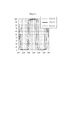
【表1】

更に、図3に、この時の透過率特性を示す。横軸は波長、縦軸は透過率を示す。図3において、点線33TS33は空気側から入射角33度、層数33層のS成分透過率特性を示し、実線45TS33は空気側から入射角45度、層数33層のS成分透過率特性を示し、破線57TS33は空気側から入射角57度、層数33層のS成分透過率特性を示す。
【0024】
本実施例においては、45度入射の時、430〜480nmの範囲で平均0.2%の低透過率、510〜570nmの範囲で平均98%の高透過率、600〜650nmの範囲で平均0.4%の低透過率が得られた。又、角度特性を半値波長巾(33度の時の短波長側の半値波長と57度の時の長波長側の半値波長の差を示し、緑成分の明るさに対応)で示すと、約48nmであつた。共に実用上問題無い特性が得られた。
【0025】
表1の結果から分かるように、本実施例の膜の特徴は、(1)全薄膜群の総光学膜厚の実施膜厚が基本膜厚の約0.96倍であり、(2)第1薄膜群の総光学膜厚の実施膜厚が基本膜厚の約1.02倍であり、(3)第2、第3薄膜群の総光学膜厚の実施膜厚が基本膜厚の約0.91倍であり、(4)2つの1λ0/4層とそれに挟まれた1つの2λ0/4層との計3層(第2群3層基本構成)からなる第2薄膜群において、実施膜厚が約3.0λ0/4〜4.5λ0/4の範囲であり、(5)連続する3つの1λ0/4層(第1群3層基本構成)からなる第1薄膜群と第2群3層基本構成からなる第2薄膜群において、1つの第2薄膜群とそれに隣接する2つの第1薄膜群の3群の合計の実施膜厚が約9.3λ0/4〜10.5λ0/4の範囲であり、(6)第1群3層基本構成からなる第1薄膜群と第2群3層基本構成からなる第2薄膜群において、1つの第1薄膜群とそれに隣接する2つの第2薄膜群の3群の合計の実施膜厚が約9.7λ0/4〜10.7λ0/4の範囲を満たしていることである。
【0026】
<実施例2>
実施例1と同様にして、第1薄膜群及び第2薄膜群をSiO2膜とTa2O5膜で構成し、11群からなる緑透過トリミングフィルターをBK7基板上に真空蒸着法により形成した。表2に、各薄膜群を含む基本構成の基本膜厚、及び透過率改善のための調整後の実施膜厚を示す。但し、使用入射角は0度である。
【0027】
更に、図4(a)に、この時の透過率特性を示す。図4(a)において、点線12TS33は空気側から入射角12度、層数33層のS成分透過率特性を示し、実線0TS33は空気側から入射角0度、層数33層の透過率特性を示す。
本実施例においては、0度入射の時、430〜480nmの範囲で平均1.2%の低透過率、510〜570nmの範囲で平均98%の高透過率、600〜650nmの範囲で平均0.2%の低透過率が得られ、実用上問題無い特性であった。
【0028】
更に、本実施例2の0度入射フィルターと実施例1の45度入射フィルターを組み合わせる事により、コントラストを向上させる事が出来た。即ち、45度入射フィルターの後に0度入射フィルターを設置する事により、入射角度に依存する不要な光(図1において、入射角33度の時の約580〜600nmの透過光、及び入射角57度の時の約485〜500nmの透過光)をカットする事が出来た。この時の特性を図2(b)に示す。図2(b)において、33*12Tsは入射角33度と12度で透過したS成分を示し、57*12Tsは入射角57度と12度で透過したS成分を示す。
【0029】
【表2】
表2の結果から分かるように、本実施例の膜の特徴は、(1)全薄膜群の総光学膜厚の実施膜厚が基本膜厚の約0.94倍であり、(2)第1薄膜群の総光学膜厚の実施膜厚が基本膜厚の約0.95倍であり、(3)第2、第3薄膜群の総光学膜厚の実施膜厚が基本膜厚の約0.94倍であり、(4)第2群3層基本構成からなる第2薄膜群において、実施膜厚が約3.4λ0/4〜4.6λ0/4の範囲であり、(5)第1群3層基本構成からなる第1薄膜群と第2群3層基本構成からなる第2薄膜群において、1つの第2薄膜群とそれに隣接する2つの第1薄膜群の3群の合計の実施膜厚が約8.7λ0/4〜9.8λ0/4の範囲であり、(6)第1群3層基本構成からなる第1薄膜群と第2群3層基本構成からなる第2薄膜群において、1つの第1薄膜群とそれに隣接する2つの第2薄膜群の3群の合計の実施膜厚が約9.9λ0/4〜10.7λ0/4の範囲を満たしていることである。
【0031】
<実施例3>
実施例1と同様にして、第1薄膜群及び第2薄膜群をAl2O3膜とTiO2膜で構成し、11群からなる緑透過トリミングフィルターをBK7基板上に真空蒸着法により形成した。表3に、各薄膜群を含む基本構成の基本膜厚、及び透過率改善のための調整後の実施膜厚を示す。但し、表3において、TiはTiO2膜(588nmでの屈折率2.30)、AはAl2O3膜(588nmでの屈折率1.63)を示す。
【0032】
更に、図5に、この時の透過率特性を示す。図5において、点線33TS33は空気側から入射角33度、層数33層のS成分透過率特性を示し、実線45TS33は空気側から入射角45度、層数33層のS成分透過率特性を示し、破線57TS33は空気側から入射角57度、層数33層のS成分透過率特性を示す。
本実施例においては、45度入射の時、430〜480nmの範囲で平均0.3%の低透過率、510〜570nmの範囲で平均98%の高透過率、600〜650nmの範囲で平均0.5%の低透過率が得られた。又、角度特性を半値波長巾で示すと、約51nmであつた。共に実用上問題無い特性が得られた。
【0033】
【表3】
表3において、第2薄膜群を構成する1層目のAl2O3膜の実施膜厚が0となっている。しかし、これは基板に接する層として全体特性の上から0が好ましいという事であり、基本構成(第2群の基本膜厚合計は約4/4λ0)を逸脱するものではない。
【0035】
表3の結果からわかるように、本実施例の膜の特徴は、(1)全薄膜群の総光学膜厚の実施膜厚が基本膜厚の約0.94倍であり、(2)第1薄膜群の総光学膜厚の実施膜厚が基本膜厚の約0.97倍であり、(3)第2、第3薄膜群の総光学膜厚の実施膜厚が基本膜厚の約0.91倍であり、(4)第2群3層基本構成からなる第2薄膜群において、実施膜厚が約3.1λ0/4〜4.0λ0/4の範囲であり、(5)第1群3層基本構成からなる第1薄膜群と第2群3層基本構成からなる第2薄膜群において、1つの第2薄膜群とそれに隣接する2つの第1薄膜群の3群の合計の実施膜厚が約9.2λ0/4〜10.3λ0/4の範囲であり、(6)第1群3層基本構成からなる第1薄膜群と第2群3層基本構成からなる第2薄膜群において、1つの第1薄膜群とそれに隣接する2つの第2薄膜群の3群の合計の実施膜厚が約9.8λ0/4〜11.0λ0/4の範囲を満たしていることである。
【0036】
<実施例4>
第1薄膜群及び第2薄膜群をSiO2膜とTa2O5膜で構成し、7群からなる緑透過トリミングフィルターをBK7基板上に真空蒸着法により形成した。表4に、基板側からの各薄膜群を含む基本構成の基本膜厚、及び透過率改善のための調整後の実施膜厚を示す。使用入射角は45度である。
【0037】
更に、図6にこの時の透過率特性を示す。図6において、点線33TS21は空気側から入射角33度、層数21層のS成分透過率特性を示し、実線45TS21は空気側から入射角45度、層数21層のS成分透過率特性を示し、破線57TS21は空気側から入射角57度、層数21層のS成分透過率特性を示す。
【0038】
本実施例においては、45度入射の時、430〜480nmの範囲で平均2.0%の低透過率、510〜570nmの範囲で平均98%の高透過率、600〜650nmの範囲で平均2.2%の低透過率が得られた。青、赤領域のモレ透過光がやや多いが、実用上は問題無かった。又、角度特性を半値波長巾で示すと、実施例1と同様約48nmであつた。
【0039】
【表4】
表4において、第2薄膜群を構成する21層目のSiO2膜の実施膜厚が略0となっている。しかし、これは空気に接する層として全体特性の上から略0が好ましいという事であり、基本構成(第2群の基本膜厚合計は約4/4λ0)を逸脱するものではない。
【0041】
表4の結果からわかるように、本実施例の膜の特徴は、(1)全薄膜群の総光学膜厚の実施膜厚が基本膜厚の約0.94倍であり、(2)第1薄膜群の総光学膜厚の実施膜厚が基本膜厚の約1.02倍であり、(3)第2、第3薄膜群の総光学膜厚の実施膜厚が基本膜厚の約0.9倍であり、(4)第2群3層基本構成からなる第2薄膜群において、実施膜厚が約2.7λ0/4〜4.3λ0/4の範囲であり、(5)第1群3層基本構成からなる第1薄膜群と第2群3層基本構成からなる第2薄膜群において、1つの第2薄膜群とそれに隣接する2つの第1薄膜群の3群の合計の実施膜厚が約9.3λ0/4〜10.3λ0/4の範囲であり、(6)第1群3層基本構成からなる第1薄膜群と第2群3層基本構成からなる第2薄膜群において、1つの第1薄膜群とそれに隣接する2つの第2薄膜群の3群の合計の実施膜厚が約9.9λ0/4〜10.6λ0/4の範囲を満たしていることである。
【0042】
<実施例5>
第1薄膜群、第2薄膜群及び第3薄膜群をSiO2膜とTa2O5膜で構成し、11群からなる緑透過トリミングフィルターをBK7基板上に真空蒸着法により形成した。表5に、基板側からの各薄膜群を含む基本構成の基本膜厚、及び透過率改善のための調整後の実施膜厚を示す。使用入射角は45度である。
【0043】
更に、図7に、この時の透過率特性を示す。図7において、点線33TS28は空気側から入射角33度、層数28層のS成分透過率特性を示し、実線45TS28は空気側から入射角45度、層数28層のS成分透過率特性を示し、破線57TS28は空気側から入射角57度、層数28層のS成分透過率特性を示す。
本実施例においては、45度入射の時、430〜480nmの範囲で平均0.2%の低透過率、510〜570nmの範囲で平均98%の高透過率、600〜650nmの範囲で平均0.4%の低透過率が得られた。又、角度特性を半値波長巾で示すと、約49nmであつた。共に実用上問題無い特性が得られた。
【0044】
【表5】
表5の結果からわかるように、本実施例の膜の特徴は、(1)全薄膜群の総光学膜厚の実施膜厚が基本膜厚の約1.0倍であり、(2)第1薄膜群の総光学膜厚の実施膜厚が基本膜厚の約1.10倍であり、(3)第2、第3薄膜群の総光学膜厚の実施膜厚が基本膜厚の約0.94倍であり、(4)第2群3層基本構成からなる第2薄膜群において、実施膜厚が約3.7λ0/4〜3.8λ0/4の範囲であり、(5)第1群3層基本構成からなる第1薄膜群と第2群3層基本構成からなる第2薄膜群において、1つの第2薄膜群とそれに隣接する2つの第1薄膜群の3群の合計の実施膜厚が約9.7λ0/4〜10.7λ0/4の範囲であり、(6)第1群3層基本構成からなる第1薄膜群と第2群3層基本構成からなる第2薄膜群において、1つの第1薄膜群とそれに隣接する2つの第2薄膜群の3群の合計の実施膜厚が約10.4λ0/4〜10.6λ0/4の範囲を満たしていることである。
【0046】
次に、本発明の比較対象として、本発明とは異なる基本構成の比較例を示した。
【0047】
<比較例1>
Ta2O5膜とSiO2膜の交互層からなる青反射特性を有する薄膜群とTa2O5膜とSiO2膜の交互層からなる赤反射特性を有する薄膜群を真空蒸着法により基板上に重ねて形成し、緑透過トリミングフィルターを得た。表6に、透過率改善のための調整後の実施膜厚を基板側から第1層目としてを示す。使用入射角は45度である。
【0048】
【表6】
更に、図8に、この時の透過率特性を示す。図8において、点線33TS40は空気側から入射角33度、層数40層のS成分透過率特性を示し、実線45TS40は空気側から入射角45度、層数40層のS成分透過率特性を示し、破線57TS40は空気側から入射角57度、層数40層のS成分透過率特性を示す。
【0050】
本比較例においては、45度入射の時、430〜480nmの範囲で平均0.5%の低透過率、510〜570nmの範囲で平均98%の高透過率、600〜650nmの範囲で平均0.1%の低透過率が得られた。又、角度特性を半値波長巾で示すと、約34nmであつた。透過率特性は本実施例と同等であるが、角度特性では劣り、明るさが不足する結果となり実用上問題であった。更に、層数が本実施例に比較して多くなるのが難点である。
【0051】
<比較例2>
特公昭60−038683号公報の図2に示される11層特性のものを実施例1と同様にして形成した。但し、第1薄膜群をSiO2膜とZrO2膜、第2薄膜群をSiO2膜とZrO2膜とし、設計波長λ0は540nm、使用入射角は0度とした。第1薄膜群はλ0/4の交互層であり、第2薄膜群は 4λ0/4−2λ0/4−4λ0/4の基本構成である。この基本構成膜厚の時の特性を図9に示す。図9において、実線0T11は空気側から入射角0度、層数11層の透過率特性を示す。
【0052】
図7から、430〜480nmの範囲の低透過率、600〜650nmの範囲の低透過率が得られず、本比較例の構成では、緑透過トリミングフィルターとして実用に適しない。
【0053】
<液晶プロジェクターの実施例>
次に、本実施形態の光学多層膜を用いたトリミングフィルターを有する液晶プロジェクターの実施例を示す。
【0054】
図10は本実施形態の光学多層膜を用いたトリミングフィルターを有する液晶プロジェクターの図である。図10において、101は光源、102は偏光板、103は本実施形態の光学多層膜を用いた、緑波長帯域の光(G)を透過し、青波長帯域の光(B)と赤波長帯域の光(R)を反射するトリミングフィルターである。104aは赤色光の偏光方向を90度変換し、青色光の偏光方向は変換しない第1の色選択性位相差板、104bは赤色光の偏光方向は変換せずに、青色光の偏光方向を90度変換する第2の色選択性位相差板、105a、105b、105cは夫々P偏光を透過し、S偏光を反射する第1、第2及び第3の偏光ビームスプリッタである。106R、106G、106Bは夫々入射した光を反射するとともに画像変調する赤用の反射型液晶表示素子、緑用の反射型液晶表示素子、青用の反射型液晶表示素子である。107は投射レンズである。
【0055】
光源101から出射した無偏光の光は、偏光板102によって直線偏光(P偏光)とされ、トリミングフィルター103に入射する。トリミングフィルター103によって、緑色光は透過されるが、青色光と赤色光は反射する。これにより、緑色光と青、赤色光とが色分解される。
【0056】
緑色光は第1の偏光ビームスプリッタ105aを透過して緑用の反射型液晶表示素子106Gに入射する。一方、トリミングフィルター103を透過した青色光と赤色光は第1の色選択性位相差板104aに入射して、ここで赤色光の偏光方向のみが90度回転させられS偏光となる。
【0057】
第2の偏光ビームスプリッタ105bは、P偏光である青色光を透過し、S偏光である赤色光を反射することでこれらを色分解し、青色光および赤色光はそれぞれ青用の反射型液晶表示素子106B及び赤用の反射型液晶表示素子106R入射する。
【0058】
緑用の反射型液晶表示素子106Gで変調された光のうちS偏光成分は第1の偏光ビームスプリッタ105aで反射し、第3の偏光ビームスプリッタ105cでも反射して投影光となる。
【0059】
青用の反射型液晶表示素子106Bで変調された光のうちS偏光成分は第2の偏光ビームスプリッタ105bで反射し、第2の色選択性位相差板104bによって偏光方向が90度回転し、P偏光となり、第3の偏光ビームスプリッタ105cを透過して、投影光となる。
【0060】
赤用の反射型液晶表示素子106Rで変調された光のうちP偏光成分は第2の偏光ビームスプリッタ105bを透過し、第2の色選択性位相差板104bを透過し、第3の偏光ビームスプリッタ105cを透過して、投影光となる。第3の偏光ビームスプリッタ105cで1つに合成された緑色光と青色光と赤色光は、投射レンズ107より投射されることによってカラー画像を表示する。
【0061】
本実施例の液晶プロジェクターは、本実施形態の光学多層膜を用いることによって、少ない層数で緑色光を透過し、青、赤色光を反射するトリミングフィルターを実現している。
【0062】
【発明の効果】
本発明により、比較的少ない層数で、特定波長域で透過率が高くなる光学多層膜を実現することが可能となった。
【図面の簡単な説明】
【図1】本発明の概略を示す図である。
【図2】(a)薄膜群の切り分け方を示す図である。(b)薄膜群の切り分け方を示す図である。
【図3】本発明の実施例1の光学多層膜の透過率特性を示す図である。
【図4】(a)本発明の実施例2の光学多層膜の透過率特性を示す図である。(b)本発明の実施例1と実施例2の光学多層膜を組み合わせたときの透過率特性を示す図である。
【図5】本発明の実施例3の光学多層膜の透過率特性を示す図である。
【図6】本発明の実施例4の光学多層膜の透過率特性を示す図である。
【図7】本発明の実施例5の光学多層膜の透過率特性を示す図である。
【図8】本発明の比較例1の光学多層膜の透過率特性を示す図である。
【図9】本発明の比較例2の光学多層膜の透過率特性を示す図である。
【図10】本実施形態のトリミングフィルターを有する液晶プロジェクターの図である。[0001]
TECHNICAL FIELD OF THE INVENTION
The present invention relates to an optical multilayer film and an optical element. In particular, the present invention relates to an optical multilayer film used in a color separation (synthesis) optical system such as a liquid crystal projector, and more particularly to a trimming filter that transmits light in a green wavelength band and reflects light in a blue and red wavelength band.
[0002]
[Prior art]
2. Description of the Related Art In a color separation (synthesis) optical system such as a liquid crystal projector, an optical system formed by combining a polarization beam splitter and an optical element (color-selective phase difference plate) for changing a polarization direction in a specific wavelength range is disclosed in Japanese Patent Application Laid-Open No. 2001-154152. No. 6,098,045.
[0003]
The color-selective phase difference plate can separate the light in that wavelength range by changing the polarization direction in a specific wavelength range and combining it with a polarizing beam splitter. It is difficult to separate light with good purity. For example, if the P-polarized light consisting of green light and red light having a continuous wavelength band is converted only to red light into S-polarized light by a color-selective phase difference plate, and green light and red light are separated by a polarizing beam splitter, the green light is converted to green light. It is difficult to separate light of a wavelength band between light and red light with high purity.
[0004]
Therefore, if green light is separated by a trimming filter using an optical multilayer film, and then blue and red light are separated (combined) by a color-selective retardation plate, the wavelength bands of blue light and red light are far apart. There is an advantage that blue and red light are easily separated (combined). The trimming filter referred to here is an optical element having an optical multilayer film that transmits light in a specific wavelength range and reflects light in other wavelength ranges.
[0005]
As a method for obtaining film characteristics having green light separation characteristics, a method of forming a thin film group having blue reflection characteristics and a thin film group having red reflection characteristics on a substrate so as to obtain green transmission and blue-red reflection characteristics is known. Are known.
[0006]
Japanese Patent Publication No. Sho 60-038683 proposes an example of a trimming filter which does not have green reflection and blue-red transmission characteristics but divides light in the blue, green and red wavelength bands as main components. In this example, when the design wavelength is lambda 0, the first thin film group consisting of alternating layers of optical thickness λ 0/4, 2λ 0/ 4 and 4.lamda 0/4 second thin film group consisting of alternating layers of A configuration including four or more groups of the two thin film groups is disclosed.
[0007]
[Problems to be solved by the invention]
However, in a two-group configuration in which a thin film group having a blue reflection characteristic and a thin film group having a red reflection characteristic are superimposed, the number of layers tends to increase in order to obtain desired characteristics. Dependent half-value wavelength shift and transmittance deterioration) were not preferable.
[0008]
The trimming filter disclosed in Japanese Patent Publication No. 60-038683, which is a prior example, divides light in the respective wavelength bands of blue, green, and red as main components, but has a low transmittance in the range of 430 to 480 nm and a wavelength of 600 nm. No low transmittance in the range of 6650 nm was obtained, and the wavelength range of high transmittance in the green transmission band was narrow.
[0009]
An object of the present invention is to provide a novel optical multilayer film having a high transmittance in a specific wavelength band such as a green wavelength band in view of the above conventional example.
[0010]
[Means for Solving the Problems]
In order to achieve the above object, the optical multilayer film of the present invention is an optical multilayer film in which the actual film thickness is determined based on the basic configuration in which the basic thickness and the layer configuration of each layer are determined. when was the lambda 0, alternating layers of the first thin film group composed of a single layer or alternating layers of optical thickness λ 0/4, and 2 [lambda] 0/4 of the single layer or lambda 0/4 and 2 [lambda] 0/4 a second thin film group consisting of the three thin-film group and the third thin film group consisting of alternating layers of 4.lamda 0/4 of the single layer or lambda 0/4 and 4.lamda 0/4, at least two kinds of thin films group And seven or more groups, and the thin film groups composed of a single layer are not adjacent to each other.
[0011]
In the basic configuration, the division of each thin film group is determined by the priority of the third thin film group, the second thin film group, and the first thin film group.
[0012]
BEST MODE FOR CARRYING OUT THE INVENTION
The green transmission trimming filter of the liquid crystal projector needs characteristics in consideration of the spectral characteristics of the light source lamp. That is, a low transmittance in the range of 430 to 480 nm, a high transmittance in the range of 510 to 570 nm, and a low transmittance in the range of 600 to 650 nm are required. However, the specific wavelength range, that is, the wavelength range of the high transmission range is not necessarily the fixed value described above, and varies depending on desired characteristics, such as a specific wavelength range of 500 to 600 nm depending on the specification.
[0013]
The trimming filter according to the present embodiment that achieves the above characteristics has a configuration in which a multilayer film in which a plurality of thin films having different optical film thicknesses are stacked is formed on a substrate. The film forming method may be a vacuum deposition method, a sputtering method or any other thin film forming method. Further, the substrate may be any substrate such as a glass substrate, a plastic substrate, or a crystal substrate.
[0014]
The multilayer film, as shown in FIG. 1, the basic structure that defines the optical thickness of each layer a center wavelength in a specific wavelength range of the desired characteristics as the design wavelength lambda 0 is determined. Next, the optical thickness of each layer of the basic configuration is adjusted to improve the transmittance. This adjustment is to change the basic film thickness, which is the optical film thickness of each layer of the basic structure, in order to obtain desired characteristics. The film thickness of each layer after the adjustment is referred to as an actual film thickness with respect to the basic film thickness. For example, even if the basic configuration is the same, the actual film thickness will be different if the wavelength range of the desired specific wavelength region is different depending on the specification, or if the used incident angle (the assumed incident angle of light) is different. The conversion from the basic film thickness to the actual film thickness is performed by a known calculation method.
[0015]
The basic configuration is composed of a plurality of thin film groups. The thin film group is a group of thin films composed of one layer or a plurality of layers classified according to the optical film thickness. (In the case of a single layer, it is not strictly a group, but here it is assumed that only one layer is included in the group.) There are three types of thin film groups: the first thin film group, the second thin film group, and the third thin film group . A design wavelength lambda 0, the first thin film group optical thickness 1λ 0/4 (= ndcosθ, n is the refractive index, d is the geometrical thickness, theta is the angle of refraction)
[0016]
Second thin film group is a laminated film in which the 2 [lambda] 0/4 layers single layer or 2 [lambda] 0/4 layers of a 1 [lambda 0/4 layers are alternately stacked.
[0017]
The third thin film group is a laminated film and a single layer or 4.lamda of 4.lamda 0/4 layer 0/4 layer and 1 [lambda 0/4 layers are alternately stacked.
[0018]
In addition, the group is divided into the third, second, and first thin film groups in order of priority, and the number of layers is maximized from the thin film group having the highest priority without departing from the definition of the group. To Further, the thin film groups composed of a single layer do not contact each other continuously. That is, it is assumed that there is a basic structure 2a on the
[0019]
The present invention achieves desired characteristics by adopting a basic configuration having a total of seven or more groups of at least two types of thin film groups among the three types of thin film groups.
[0020]
【Example】
Hereinafter, examples of the present invention will be described, but the present invention is not limited thereto.
[0021]
<Example 1>
The first thin film group and the second thin film group were composed of a SiO 2 film and a Ta 2 O 5 film, and a green transmission trimming filter composed of 11 groups was formed on a BK7 substrate by a vacuum evaporation method. Table 1 shows the basic film thickness of the basic configuration including each thin film group having the substrate side as the first layer, and the practical film thickness after adjustment for improving transmittance. However, in Table 1, the design wavelength lambda 0 is 537 nm, the film thickness represents a multiple of λ 0/4, Ta is the Ta 2 O 5 film (refractive index at 588 nm 2.15), S is SiO 2 film (588 nm Is 1.46). The used incident angle is 45 degrees.
[0022]
[Table 1]
FIG. 3 shows the transmittance characteristics at this time. The horizontal axis indicates the wavelength, and the vertical axis indicates the transmittance. In FIG. 3, a dotted line 33TS33 indicates the incident angle of 33 degrees from the air side and the S component transmittance characteristics of the 33 layers, and the solid line 45TS33 indicates the incident angle of 45 degrees from the air side and the S component transmittance characteristics of the 33 layers. The broken line 57TS33 indicates the S component transmittance characteristic of the 33 layers with an incident angle of 57 degrees from the air side.
[0024]
In this embodiment, at 45 ° incidence, low transmittance of 0.2% on average in the range of 430 to 480 nm, high transmittance of 98% on average in the range of 510 to 570 nm, and 0 on average in the range of 600 to 650 nm. A low transmission of 0.4% was obtained. In addition, when the angle characteristic is represented by a half-value wavelength width (indicating the difference between the half-value wavelength at the short wavelength side at 33 degrees and the half-value wavelength at the long wavelength side at 57 degrees and corresponding to the brightness of the green component), It was 48 nm. In both cases, characteristics having no practical problems were obtained.
[0025]
As can be seen from the results in Table 1, the characteristics of the film of this example are as follows: (1) the total optical film thickness of all thin film groups is about 0.96 times the basic film thickness; The actual film thickness of the total optical thickness of one thin film group is about 1.02 times the basic film thickness, and (3) the practical film thickness of the total optical film thickness of the second and third thin film groups is about 1.0% of the basic film thickness. 0.91 times, (4) two 1 [lambda 0/4 layer and one 2 [lambda] 0/4 layers and a total of three layers a second thin film group consisting of (second group third layer basic structure) sandwiched therewith ranges exemplary thickness of about 3.0λ 0 /4~4.5λ 0/4, ( 5) a first thin film made of three 1 [lambda 0/4 successive layers (first group includes three layers basic configuration) in the second thin film group consisting of the group and the second group third layer basic structure, exemplary total thickness of three groups of one second thin film group and the two first films group adjacent thereto is about 9.3λ 0/4 ~ 10.5λ 0 / (6) In the first thin film group consisting of the first group three-layer basic structure and the second thin film group consisting of the second group three-layer basic structure, one first thin film group and two adjacent two thin film groups it is that the total carried thickness of the three groups of the second thin film group meets the range of about 9.7λ 0 /4~10.7λ 0/4.
[0026]
<Example 2>
In the same manner as in Example 1, the first thin film group and the second thin film group were composed of a SiO 2 film and a Ta 2 O 5 film, and a green transmission trimming filter composed of 11 groups was formed on a BK7 substrate by a vacuum deposition method. . Table 2 shows the basic film thickness of the basic structure including each thin film group and the practical film thickness after adjustment for improving transmittance. However, the used incident angle is 0 degree.
[0027]
FIG. 4A shows the transmittance characteristics at this time. In FIG. 4 (a), a dotted line 12TS33 indicates the incident angle of 12 degrees from the air side and the S component transmittance characteristics of 33 layers, and the solid line 0TS33 indicates an incident angle of 0 degrees from the air side and the transmittance characteristics of 33 layers. Is shown.
In this embodiment, at 0 degree incidence, a low transmittance of 1.2% on average in the range of 430 to 480 nm, a high transmittance of 98% on average in the range of 510 to 570 nm, and an average of 0% in the range of 600 to 650 nm. A low transmittance of 0.2% was obtained, and the characteristics were not problematic in practical use.
[0028]
Further, by combining the 0-degree incident filter of the second embodiment and the 45-degree incident filter of the first embodiment, the contrast could be improved. That is, by installing a 0-degree incident filter after the 45-degree incident filter, unnecessary light depending on the incident angle (in FIG. 1, transmitted light of about 580 to 600 nm at an incident angle of 33 degrees and an incident angle of 57 degrees). About 485 to 500 nm at the time of transmission). The characteristics at this time are shown in FIG. In FIG. 2B, 33 * 12Ts indicates an S component transmitted at incident angles of 33 degrees and 12 degrees, and 57 * 12Ts indicates an S component transmitted at incident angles of 57 degrees and 12 degrees.
[0029]
[Table 2]
As can be seen from the results in Table 2, the characteristics of the film of this example are as follows: (1) The total optical film thickness of all thin film groups is about 0.94 times the basic film thickness; The actual film thickness of the total optical thickness of one thin film group is about 0.95 times the basic film thickness, and (3) the practical film thickness of the total optical film thickness of the second and third thin film groups is about 0.9% of the basic film thickness. 0.94 times, (4) in the second thin film group formed of the second group third layer basic structure ranges exemplary thickness of about 3.4λ 0 /4~4.6λ 0/4, ( 5 ) In the first thin film group consisting of the first group three-layer basic structure and the second thin film group consisting of the second group three-layer basic structure, three groups of one second thin film group and two adjacent first thin film groups an exemplary thickness of about 8.7λ 0 /4~9.8λ 0/4 range of total (6) from the first thin film group consisting of the first group includes three layers basic configuration second group third layer basic structure The second thin film group There are, by implementation total thickness of three groups of one first thin film group and two second thin film group adjacent thereto satisfies the range of about 9.9λ 0 /4~10.7λ 0/4 is there.
[0031]
<Example 3>
In the same manner as in Example 1, the first thin film group and the second thin film group were composed of an Al 2 O 3 film and a TiO 2 film, and a green transmission trimming filter composed of 11 groups was formed on a BK7 substrate by a vacuum deposition method. . Table 3 shows the basic film thickness of the basic structure including each thin film group and the practical film thickness after adjustment for improving the transmittance. However, in Table 3, Ti indicates a TiO 2 film (refractive index at 588 nm 2.30), and A indicates an Al 2 O 3 film (refractive index at 588 nm 1.63).
[0032]
FIG. 5 shows the transmittance characteristics at this time. In FIG. 5, a dotted line 33TS33 indicates an incident angle of 33 degrees from the air side and the S component transmittance characteristics of 33 layers, and a solid line 45TS33 indicates an incident angle of 45 degrees from the air side and the S component transmittance characteristics of 33 layers. The broken line 57TS33 indicates the S component transmittance characteristic of the 33 layers with an incident angle of 57 degrees from the air side.
In this embodiment, at 45 ° incidence, low transmittance of 0.3% on average in the range of 430 to 480 nm, high transmittance of 98% on average in the range of 510 to 570 nm, and 0 on average in the range of 600 to 650 nm. A low transmittance of 0.5% was obtained. In addition, the angular characteristic was about 51 nm when expressed by a half-value wavelength width. In both cases, characteristics having no practical problems were obtained.
[0033]
[Table 3]
In Table 3, the practical film thickness of the first Al 2 O 3 film constituting the second thin film group is 0. However, this means that 0 is preferable from the viewpoint of the overall characteristics of the layer in contact with the substrate, and does not deviate from the basic configuration (the total basic film thickness of the second group is about 4 / 4λ 0 ).
[0035]
As can be seen from the results in Table 3, the characteristics of the film of the present embodiment are as follows: (1) the total optical film thickness of all thin film groups is about 0.94 times the basic film thickness; The actual film thickness of the total optical thickness of one thin film group is about 0.97 times the basic film thickness, and (3) the practical film thickness of the total optical film thickness of the second and third thin film groups is about 0.9% of the basic film thickness. 0.91 times, (4) in the second thin film group formed of the second group third layer basic structure ranges exemplary thickness of about 3.1λ 0 /4~4.0λ 0/4, ( 5 ) In the first thin film group consisting of the first group three-layer basic structure and the second thin film group consisting of the second group three-layer basic structure, three groups of one second thin film group and two adjacent first thin film groups an exemplary thickness of about 9.2λ 0 /4~10.3λ 0/4 range of total (6) from the first thin film group consisting of the first group includes three layers basic configuration second group third layer basic structure Second thin film group Oite, the exemplary total thickness of three groups of one first thin film group and two second thin film group adjacent thereto satisfies the range of about 9.8λ 0 /4~11.0λ 0/4 It is.
[0036]
<Example 4>
The first thin film group and the second thin film group were composed of a SiO 2 film and a Ta 2 O 5 film, and a green transmission trimming filter composed of seven groups was formed on a BK7 substrate by a vacuum evaporation method. Table 4 shows the basic film thickness of the basic structure including each thin film group from the substrate side and the practical film thickness after adjustment for improving transmittance. The used incident angle is 45 degrees.
[0037]
FIG. 6 shows the transmittance characteristics at this time. In FIG. 6, a dotted line 33TS21 indicates an incident angle of 33 degrees from the air side and S component transmittance characteristics of 21 layers, and a solid line 45TS21 indicates an incident angle of 45 degrees from the air side and S component transmittance characteristics of 21 layers. The dashed line 57TS21 indicates the S component transmittance characteristic of 21 layers with an incident angle of 57 degrees from the air side.
[0038]
In the present embodiment, at 45 ° incidence, low transmittance of 2.0% on average in the range of 430 to 480 nm, high transmittance of 98% on average in the range of 510 to 570 nm, and 2 on average in the range of 600 to 650 nm. A low transmission of 0.2% was obtained. Although the amount of transmitted light in the blue and red regions is slightly large, there was no problem in practical use. In addition, when the angle characteristics were expressed by a half-value wavelength width, it was about 48 nm as in Example 1.
[0039]
[Table 4]
In Table 4, the practical thickness of the 21st SiO 2 film constituting the second thin film group is substantially zero. However, this means that the layer in contact with air is preferably substantially 0 from the viewpoint of the overall characteristics, and does not deviate from the basic configuration (the total basic film thickness of the second group is about 4 / 4λ 0 ).
[0041]
As can be seen from the results in Table 4, the characteristics of the film of this example are as follows: (1) The total optical film thickness of all thin film groups is about 0.94 times the basic film thickness; The actual film thickness of the total optical thickness of one thin film group is about 1.02 times the basic film thickness, and (3) the practical film thickness of the total optical film thickness of the second and third thin film groups is about 1.0% of the basic film thickness. 0.9 times, (4) in the second thin film group formed of the second group third layer basic structure ranges exemplary thickness of about 2.7λ 0 /4~4.3λ 0/4, ( 5 ) In the first thin film group consisting of the first group three-layer basic structure and the second thin film group consisting of the second group three-layer basic structure, three groups of one second thin film group and two adjacent first thin film groups an exemplary thickness of about 9.3λ 0 /4~10.3λ 0/4 range of total (6) from the first thin film group consisting of the first group includes three layers basic configuration second group third layer basic structure The second thin film group There are, by implementation total thickness of three groups of one first thin film group and two second thin film group adjacent thereto satisfies the range of about 9.9λ 0 /4~10.6λ 0/4 is there.
[0042]
<Example 5>
The first thin film group, the second thin film group, and the third thin film group were composed of a SiO 2 film and a Ta 2 O 5 film, and a green transmission trimming filter composed of 11 groups was formed on a BK7 substrate by a vacuum evaporation method. Table 5 shows the basic film thickness of the basic structure including each thin film group from the substrate side and the practical film thickness after adjustment for improving transmittance. The used incident angle is 45 degrees.
[0043]
FIG. 7 shows the transmittance characteristics at this time. In FIG. 7, a dotted line 33TS28 shows an S component transmittance characteristic of the 28 layers with an incident angle of 33 degrees from the air side, and a solid line 45TS28 shows an S component transmittance characteristic of an 28 angle with the 28 layers from the air side. The dashed line 57TS28 shows the S component transmittance characteristics of an incident angle of 57 degrees from the air side and 28 layers.
In this embodiment, at 45 ° incidence, low transmittance of 0.2% on average in the range of 430 to 480 nm, high transmittance of 98% on average in the range of 510 to 570 nm, and 0 on average in the range of 600 to 650 nm. A low transmission of 0.4% was obtained. In addition, when the angle characteristics were expressed in terms of the half-value wavelength width, it was about 49 nm. In both cases, characteristics having no practical problems were obtained.
[0044]
[Table 5]
As can be seen from the results in Table 5, the characteristics of the film of this example are as follows: (1) the total optical film thickness of all thin film groups is about 1.0 times the basic film thickness; The actual film thickness of the total optical thickness of one thin film group is about 1.10 times the basic film thickness, and (3) the practical film thickness of the total optical film thickness of the second and third thin film groups is about 0.94 times, (4) in the second thin film group formed of the second group third layer basic structure ranges exemplary thickness of about 3.7λ 0 /4~3.8λ 0/4, ( 5 ) In the first thin film group consisting of the first group three-layer basic structure and the second thin film group consisting of the second group three-layer basic structure, three groups of one second thin film group and two adjacent first thin film groups an exemplary thickness of about 9.7λ 0 /4~10.7λ 0/4 range of total (6) from the first thin film group consisting of the first group includes three layers basic configuration second group third layer basic structure The second thin film group There are, by implementation total thickness of three groups of one first thin film group and two second thin film group adjacent thereto satisfies the range of about 10.4λ 0 /4~10.6λ 0/4 is there.
[0046]
Next, a comparative example of a basic configuration different from the present invention was shown as a comparative object of the present invention.
[0047]
<Comparative Example 1>
The Ta 2 O 5 film and the SiO 2 film of the thin film group having blue reflection characteristic of alternating layers and the Ta 2 O 5 film and the substrate a thin film group by vacuum deposition with a red reflective properties of alternating layers of SiO 2 film And a green transmission trimming filter was obtained. Table 6 shows, as the first layer from the substrate side, the actual thickness after adjustment for improving the transmittance. The used incident angle is 45 degrees.
[0048]
[Table 6]
FIG. 8 shows transmittance characteristics at this time. In FIG. 8, a dotted line 33TS40 shows an S component transmittance characteristic of an incident angle of 33 degrees from the air side and 40 layers, and a solid line 45TS40 shows an incident angle of 45 degrees from the air side and an S component transmittance characteristic of 40 layers. The dashed line 57TS40 shows the S component transmittance characteristics of an incident angle of 57 degrees from the air side and 40 layers.
[0050]
In this comparative example, at 45 degrees incidence, low transmittance of 0.5% on average in the range of 430-480 nm, high transmittance of 98% on average in the range of 510-570 nm, and 0 average in the range of 600-650 nm. A low transmission of 0.1% was obtained. In addition, when the angle characteristics were expressed by a half-value wavelength width, it was about 34 nm. Although the transmittance characteristics are the same as those of this embodiment, the angle characteristics are inferior and the brightness is insufficient, which is a practical problem. Further, it is difficult to increase the number of layers as compared with this embodiment.
[0051]
<Comparative Example 2>
An 11-layer structure shown in FIG. 2 of Japanese Patent Publication No. 60-038683 was formed in the same manner as in Example 1. However, the first thin film group was an SiO 2 film and a ZrO 2 film, and the second thin film group was an SiO 2 film and a ZrO 2 film. The design wavelength λ 0 was 540 nm, and the incident angle used was 0 °. First thin film group is alternating layers of λ 0/4, the second thin film group is a basic configuration of 4λ 0 / 4-2λ 0 / 4-4λ 0 /4. FIG. 9 shows characteristics at the time of this basic constituent film thickness. In FIG. 9, a solid line 0T11 indicates the transmittance characteristics of the 11 layers with an incident angle of 0 ° from the air side.
[0052]
From FIG. 7, a low transmittance in the range of 430 to 480 nm and a low transmittance in the range of 600 to 650 nm cannot be obtained, and the configuration of this comparative example is not suitable for practical use as a green transmission trimming filter.
[0053]
<Example of liquid crystal projector>
Next, an example of a liquid crystal projector having a trimming filter using the optical multilayer film of the present embodiment will be described.
[0054]
FIG. 10 is a diagram of a liquid crystal projector having a trimming filter using the optical multilayer film of the present embodiment. In FIG. 10,
[0055]
Non-polarized light emitted from the
[0056]
The green light passes through the first
[0057]
The second polarization beam splitter 105b transmits blue light that is p-polarized light and color-separates red light that is s-polarized light by reflecting the red light. The blue light and the red light are each a reflective liquid crystal display for blue. The light enters the element 106B and the reflective liquid
[0058]
Of the light modulated by the green reflective liquid
[0059]
The S-polarized light component of the light modulated by the blue reflective liquid crystal display element 106B is reflected by the second polarizing beam splitter 105b, and the polarization direction is rotated by 90 degrees by the second color-selective phase difference plate 104b. The light becomes P-polarized light, passes through the third
[0060]
The P-polarized light component of the light modulated by the red reflective liquid
[0061]
The liquid crystal projector of the present embodiment realizes a trimming filter that transmits green light and reflects blue and red light with a small number of layers by using the optical multilayer film of the present embodiment.
[0062]
【The invention's effect】
According to the present invention, it has become possible to realize an optical multilayer film having a high transmittance in a specific wavelength region with a relatively small number of layers.
[Brief description of the drawings]
FIG. 1 is a diagram showing an outline of the present invention.
FIG. 2A is a diagram showing a method of dividing a thin film group. (B) It is a figure showing how to divide a thin film group.
FIG. 3 is a diagram illustrating transmittance characteristics of the optical multilayer film according to the first embodiment of the present invention.
FIG. 4 (a) is a diagram illustrating transmittance characteristics of an optical multilayer film according to a second embodiment of the present invention. (B) is a diagram showing transmittance characteristics when the optical multilayer films of Example 1 and Example 2 of the present invention are combined.
FIG. 5 is a diagram illustrating transmittance characteristics of an optical multilayer film according to Example 3 of the present invention.
FIG. 6 is a diagram illustrating transmittance characteristics of an optical multilayer film according to Example 4 of the present invention.
FIG. 7 is a diagram showing transmittance characteristics of an optical multilayer film of Example 5 of the present invention.
FIG. 8 is a diagram illustrating transmittance characteristics of the optical multilayer film of Comparative Example 1 of the present invention.
FIG. 9 is a diagram illustrating transmittance characteristics of an optical multilayer film of Comparative Example 2 of the present invention.
FIG. 10 is a diagram of a liquid crystal projector having a trimming filter according to the embodiment.
Claims (15)
但し、前記基本構成において、第3薄膜群、第2薄膜群、第1薄膜群の優先順位で各薄膜群の区切りは決定される。An optical multilayer film which defines the actual film thickness based on the basic structure that defines the basic thickness and layer structure of each layer, when the basic configuration in which the lambda 0 the design wavelength, the optical thickness lambda 0/4 a first thin film group composed of a single layer or alternating layers of a second thin film group consisting of alternating layers of 2 [lambda] 0/4 of the single layer or lambda 0/4 and 2λ 0/4, 4λ 0/ 4 monolayer or lambda 0/4 and 4.lamda 0/4 of the three thin-film group and the third thin film group consisting of alternating layers of, comprising at least two thin film groups 7 or more groups, and a thin film group to each other consisting of a single layer Are not adjacent to each other.
However, in the basic configuration, the division of each thin film group is determined by the priority order of the third thin film group, the second thin film group, and the first thin film group.
但し、前記基本構成において、第3薄膜群、第2薄膜群、第1薄膜群の優先順位で各薄膜群の区切りは決定される。The method for designing an optical multilayer film includes a step of setting a basic configuration in which a basic thickness and a layer configuration of each layer are determined, and a step of determining an actual film thickness based on the basic configuration. when the wavelength is lambda 0, alternating with the first thin film group composed of a single layer or alternating layers of optical thickness λ 0/4, and 2 [lambda] 0/4 of the single layer or lambda 0/4 and 2 [lambda] 0/4 a second thin film group of layers, of the three thin-film group and the third thin film group consisting of alternating layers of 4.lamda 0/4 of the single layer or lambda 0/4 and 4.lamda 0/4, at least two kinds of thin films A method for designing an optical multilayer film, comprising seven or more groups, and wherein the thin film groups composed of a single layer are not adjacent to each other.
However, in the basic configuration, the division of each thin film group is determined by the priority order of the third thin film group, the second thin film group, and the first thin film group.
Priority Applications (1)
| Application Number | Priority Date | Filing Date | Title |
|---|---|---|---|
| JP2002204283A JP2004045853A (en) | 2002-07-12 | 2002-07-12 | Optical multi-layered film and optical element |
Applications Claiming Priority (1)
| Application Number | Priority Date | Filing Date | Title |
|---|---|---|---|
| JP2002204283A JP2004045853A (en) | 2002-07-12 | 2002-07-12 | Optical multi-layered film and optical element |
Publications (2)
| Publication Number | Publication Date |
|---|---|
| JP2004045853A true JP2004045853A (en) | 2004-02-12 |
| JP2004045853A5 JP2004045853A5 (en) | 2005-10-27 |
Family
ID=31709933
Family Applications (1)
| Application Number | Title | Priority Date | Filing Date |
|---|---|---|---|
| JP2002204283A Pending JP2004045853A (en) | 2002-07-12 | 2002-07-12 | Optical multi-layered film and optical element |
Country Status (1)
| Country | Link |
|---|---|
| JP (1) | JP2004045853A (en) |
Cited By (3)
| Publication number | Priority date | Publication date | Assignee | Title |
|---|---|---|---|---|
| JP2008085232A (en) * | 2006-09-28 | 2008-04-10 | Casio Comput Co Ltd | Liquid crystal display device |
| JP2011164549A (en) * | 2010-02-15 | 2011-08-25 | Kowa Co | Color separation optical system excellent in color reproducibility |
| JP2012038690A (en) * | 2010-08-11 | 2012-02-23 | Toshiba Corp | Backlight and liquid crystal display device |
-
2002
- 2002-07-12 JP JP2002204283A patent/JP2004045853A/en active Pending
Cited By (4)
| Publication number | Priority date | Publication date | Assignee | Title |
|---|---|---|---|---|
| JP2008085232A (en) * | 2006-09-28 | 2008-04-10 | Casio Comput Co Ltd | Liquid crystal display device |
| JP2011164549A (en) * | 2010-02-15 | 2011-08-25 | Kowa Co | Color separation optical system excellent in color reproducibility |
| JP2012038690A (en) * | 2010-08-11 | 2012-02-23 | Toshiba Corp | Backlight and liquid crystal display device |
| US8643805B2 (en) | 2010-08-11 | 2014-02-04 | Kabushiki Kaisha Toshiba | Backlight and liquid crystal display device |
Similar Documents
| Publication | Publication Date | Title |
|---|---|---|
| US7562984B2 (en) | Polarizing beam splitter and projection apparatus having the same | |
| JP4574439B2 (en) | Polarization separating element and projection apparatus having the same | |
| JP4174216B2 (en) | OPTICAL ELEMENT HAVING BARRIER LAYER, OPTICAL SYSTEM, AND PROJECTION PROJECTOR DEVICE | |
| CA2480648C (en) | Dichroic mirror and projection-type display unit | |
| EP1510838A1 (en) | Polarization beam splitter, optical system and image displaying apparatus using the same | |
| US8094246B2 (en) | Polarization conversion device, polarized illumination optical device, and liquid crystal projector | |
| US8035759B2 (en) | Polarization conversion device, polarized illumination optical device, and liquid crystal projector | |
| US5999321A (en) | Dichroic filters with low nm per degree sensitivity | |
| EP1278381A2 (en) | Projection image display apparatus | |
| JPH11101913A (en) | Optical element | |
| JPH11211916A (en) | Polarized beam splitter | |
| JP3679746B2 (en) | Optical element, liquid crystal projector and camera using the same | |
| JP2006133402A (en) | Polarized beam splitter and optical system having the same | |
| JP2012226208A (en) | Polarization separation element, and polarization conversion element and image projection device using the same | |
| JP3584257B2 (en) | Polarizing beam splitter | |
| JP4054623B2 (en) | Optical multilayer film and optical element | |
| JP2004045853A (en) | Optical multi-layered film and optical element | |
| JP2013250322A (en) | Image display device | |
| JP4537115B2 (en) | Polarization separation prism | |
| JP2008058561A (en) | Optical filter and color separation prism | |
| JP2001318221A (en) | Optical filter intercepting long wavelength, optical filter intercepting short wavelength, cross prism, cross mirror and liquid crystal projector | |
| JP2003014932A (en) | Polarized beam splitter and method for fabricating polarized beam splitter | |
| JP2001350024A (en) | Polarizing beam splitter | |
| JP2001183524A (en) | Projection type display device | |
| JP2008116714A (en) | Optical filter and color separation prism |
Legal Events
| Date | Code | Title | Description |
|---|---|---|---|
| A521 | Written amendment |
Free format text: JAPANESE INTERMEDIATE CODE: A523 Effective date: 20050706 |
|
| A621 | Written request for application examination |
Free format text: JAPANESE INTERMEDIATE CODE: A621 Effective date: 20050706 |
|
| A977 | Report on retrieval |
Free format text: JAPANESE INTERMEDIATE CODE: A971007 Effective date: 20060524 |
|
| A131 | Notification of reasons for refusal |
Free format text: JAPANESE INTERMEDIATE CODE: A131 Effective date: 20060606 |
|
| A521 | Written amendment |
Free format text: JAPANESE INTERMEDIATE CODE: A523 Effective date: 20060807 |
|
| A02 | Decision of refusal |
Free format text: JAPANESE INTERMEDIATE CODE: A02 Effective date: 20070904 |