JP2004010467A - Method for growing compound semiconductor single crystal - Google Patents
Method for growing compound semiconductor single crystal Download PDFInfo
- Publication number
- JP2004010467A JP2004010467A JP2002170815A JP2002170815A JP2004010467A JP 2004010467 A JP2004010467 A JP 2004010467A JP 2002170815 A JP2002170815 A JP 2002170815A JP 2002170815 A JP2002170815 A JP 2002170815A JP 2004010467 A JP2004010467 A JP 2004010467A
- Authority
- JP
- Japan
- Prior art keywords
- growth
- single crystal
- compound semiconductor
- semiconductor single
- melt
- Prior art date
- Legal status (The legal status is an assumption and is not a legal conclusion. Google has not performed a legal analysis and makes no representation as to the accuracy of the status listed.)
- Pending
Links
Images

Landscapes
- Crystals, And After-Treatments Of Crystals (AREA)
Abstract
Description
【0001】
【発明の属する技術分野】
本発明は、化合物半導体単結晶の成長方法に関するものである。
【0002】
【従来の技術】
III−V族化合物半導体はその単結晶の高品質化により、高速集積回路、光−電子集積回路やその他の電子素子に広く用いられるようになってきた。なかでも、砒化ガリウム(GaAs)は電子移動度がシリコンに比べて早く、107Ω・cm以上の比抵抗のウエハが製造容易という特徴がある。現在では上記GaAsの単結晶は、主に液体封止引き上げ法(LEC法:Liquid Encapsulated Czochralski法)により製造されている。
【0003】
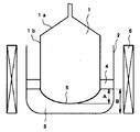
図2に、GaAs単結晶の製造装置として広く使用されているLEC法による結晶引上装置の概略を示す。
【0004】
図において、21は結晶成長用高温炉の耐圧容器であり、耐圧容器21内には下側から下軸22が挿入され、この下軸22の先端にペデスタル23を介してサセプタ24が支持されている。サセプタ24内にはPBN製るつぼ2が配置されている。サセプタ24の周囲にはヒータ6が設けられており、サセプタ24を介してPBN製るつぼ2を周囲から加熱できるようになっている。下軸22は図示しない回転機構に接続されており、一定の回転速度で回転されるようになっている。また、耐圧容器21の上側からは下軸22と同軸的に上軸29が挿入され、その下端に設けられた種結晶ホルダ30に所望の方位を持った種結晶31が取り付けられる。この上軸29は、図示しない回転・昇降機構によってPBN製るつぼ2とは逆向きに軸回転されると共に、昇降移動されるようになっている。上軸29の途中には重量センサ32が設けられており、これによって成長過程の結晶重量を検知できるようになっている。
【0005】
結晶成長の際には、先ず、PBN製るつぼ2の中にGaAs多結晶原料26を14,000gと、B2O3液体封止剤27を4,000g入れ、耐圧容器21内を真空排気し、その後窒素またはアルゴンなどの不活性ガスで40気圧程度に加圧し、主ヒータ6に通電してPBN製るつぼ2の内部を昇温させる。500℃前後で液体封止剤(B2O3)27が軟化、融解して、GaAs多結晶原料26を覆う。引き続き昇温させ、PBN製るつぼ2内部の温度を1,238℃以上とし、多結晶原料26を融解させる。次に、耐圧容器21内を5〜20気圧に減圧した後、種結晶31を降下させ、その先端を原料融液に浸して種付けを行う。その後、ヒータ6の温度を下げながら、上軸29を9〜12mm/hrの速度で引き上げていき、重量センサ32で結晶重量を検知しながら、ヒータ6の出力を制御してGaAs単結晶を成長させる。
【0006】
【発明が解決しようとする課題】
しかしながら、化合物半導体単結晶を成長する技術は非常に難しく、加熱手段のヒータ及び、熱遮蔽筒等の部材(ホットゾーンと呼ばれる。以下HZと記す)の配置、形状、材質等により、より細かく影響を受けるため、再現性の良い化合物半導体単結晶の成長条件を得るのは難しい。
【0007】
化合物半導体単結晶の成長条件を再現性良く得るための要因は、HZの配置、形状、材質等HZに係るものと考えてきた。ところが、HZの配置、形状、材質等の条件の安定化が図られるにつれ、その要因がHZのみにあるのではなく、根本的には固液界面形状を如何に制御するかが、単結晶を得るための大きな要因であることが明確になってきた。
【0008】
LEC法では、固液界面の形状の制御が、単結晶を得るうえで重要な要因である。しかし、これまでのところ固液界面形状を規定する技術については、これを開示した文献が無い。
【0009】
そこで、本発明の目的は、上記課題を解決し、LEC法において、前記技術の問題点を解消し、再現性良く化合物半導体単結晶を得ることができるように固液界面形状を規定する化合物半導体単結晶の成長方法を提供することにある。
【0010】
【課題を解決するための手段】
上記目的を達成するため、本発明は、次のように構成したものである。
【0011】
請求項1の発明は、不活性ガスを充填した耐圧容器内に収容され加熱されたるつぼに、原料融液、液体封止剤を収納し、種結晶を原料融液に接触させつつ種結晶とるつぼとを相対的に移動させて単結晶を成長させるLEC法による化合物半導体単結晶の製造方法において、 成長過程全般において固液界面形状が常に融液側に凸であるように維持して化合物半導体単結晶を成長することを特徴とする。
【0012】
請求項2の発明は、請求項1記載の成長方法において、成長方向の軸断面(縦断面)の融液の厚さBに対する固液界面の凸の大きさAの度合いA/Bを、成長初期の増径部及び成長終期の減径部を除く定径部において、0.2以上、0.9未満の範囲、好ましくは0.2以上、0.8以下の範囲にあるように維持して化合物半導体単結晶を成長することを特徴とする。
【0013】
請求項3の発明は、請求項1記載の成長方法において、成長方向の軸断面の融液の厚さBに対する固液界面の凸の大きさAの度合いA/Bが、成長初期の増径部及び成長終期の減径部を除く定径部において、0.2以上、0.9未満の範囲、好ましくは0.2以上、0.8以下の範囲にあるように、ホットゾーンの配置、形状、材質等を変更することにより調整して化合物半導体単結晶を成長することを特徴とする。
【0014】
請求項4の発明は、請求項1〜3のいずれかに記載の成長方法において、直径が100mm以上の大口径の結晶を成長することを特徴とする。
【0015】
<発明の要点>
固液界面が融液側へ凹の場合は、成長過程全般、または成長のある一定期間に係わらず、リネージや亜粒界が集積され易く、単結晶を得る再現性が低く、当然ながら収率も低くなる。
【0016】
本発明は、LEC法において固液界面形状が成長過程全般に渡り、常に融液側に凸とすることで、再現性よく、且つ高収率で化合物半導体単結晶を得ることを可能にしたものである。
【0017】
また本発明者等は、固液界面の融液側への凸の度合いに関し、鋭意研究努力した結果、次のような関係を導き出した。
【0018】
すなわち、成長初期の増径部、成長終期の減径部を除く定径部において、固液界面の融液側への凸の度合い、つまり成長方向の軸断面の融液の厚さBに対する固液界面の凸の大きさAの度合いA/Bが、0.2未満の場合は、温度変動などの微細な成長環境の変動により固液界面が融液側へ凹となり易く、リネージや亜粒界が発生し易くなり、芳しくない。
【0019】
また、成長初期の増径部、成長終期の減径部を除く定径部において、固液界面の融液側への凸の度合い、つまり成長方向の軸断面の融液の厚さBに対する固液界面の凸の大きさAの度合いA/Bが、0.8を越える場合は、温度変動などの微細な成長環境の変動により、固液界面の融液側への凸の度合いが大きくなり易く、固化後の結晶と融液を収納するるつぼが接触し、結晶成長が困難となる。この傾向は、上記固液界面の融液側への凸の度合いA/Bが、0.9を越えた場合に、特に顕著となる。
【0020】
よって、成長初期の増径部及び成長終期の減径部を除く定径部において、固液界面の融液側への凸の度合いA/Bを0.2以上、0.9未満の範囲、好ましくは0.2〜0.8の範囲にあるように、固液界面形状を規定し、これを、ホットゾーンの配置、形状、材質等を変更して調整することにより、維持すれば、直径が100mm以上の大口径の化合物半導体単結晶を再現性良く成長することができる。
【0021】
【発明の実施の形態】
以下、本発明を図示の実施形態に基づいて説明する。
【0022】
図1は、LEC法での化合物半導体単結晶の成長過程を成長方向の軸断面(縦断面)で示したものであり、成長装置の基本構造は図2と同じである。
【0023】
図1に示すように、不活性ガスを充填した耐圧容器21(図2参照)内に収容され、ヒータ6により加熱されたるつぼ2に、化合物半導体融液3、液体封止剤4を収納し、化合物半導体単結晶1を成長させる。
【0024】
ここで、化合物半導体融液3と化合物半導体単結晶1の境界が固液界面5となる。固液界面5の融液側への凸の度合いは、成長方向の軸断面の融液3の厚さBと、固液界面5の凸の大きさAとの比A/Bで示される。固液界面の融液側への凸の度合いA/Bを、化合物半導体単結晶1の成長初期の増径部1a及び成長終期の減径部を除く定径部1bの成長において、A/B値が0.2以上、0.9未満の範囲、好ましくは0.2〜0.8の範囲にあるように、固液界面形状を規定する。そして、この固液界面形状を定径部1bの成長時に維持して、化合物半導体単結晶1を成長する。固液界面5の融液側への凸の度合いA/Bの調整は、熱遮蔽筒等の部材であるホットゾーンHZの配置、形状等を変更することによって調整する。
【0025】
かくすることにより、直径が100mm以上の大口径の化合物半導体単結晶1を再現性良く、且つ高収率で成長することができる。
【0026】
<実施例>
本発明の効果を確認するため、実施例として、化合物半導体の一種である砒化ガリウムの単結晶を成長した。
【0027】
すなわち、結晶直径100mm、結晶長さ400mmの砒化ガリウム(GaAs)の単結晶成長において、固液界面5の融液側への凸の度合いA/B(成長方向の軸断面の融液の厚さBに対する固液界面の凸の大きさAの度合い)が、成長初期の増径部及び成長終期の減径部を除く定径部1bの成長において、0.2以上、0.9未満の範囲になるように、HZの配置、形状を調整して、単結晶成長を50回行った。その結果、結晶の種付けから結晶成長最終部まで全域単結晶(All Single)は95%以上の確率で得られた。
【0028】
<比較例1>
実施例と同様に結晶直径100mm、結晶長さ400mmの砒化ガリウムの単結晶成長において、固液界面の融液側への凸の度合い、つまり成長方向の軸断面の融液の厚さBに対する固液界面の凸の大きさAの度合いA/Bが、成長初期の増径部及び成長終期の減径部を除く定径部1bにおいて、0.2未満(なお、この場合には固液界面5が融液側へ凹の場合を含む)になるように、HZの配置、形状を調整して単結晶成長を50回行った。その結果、結晶の種付けから結晶成長最終部まで全域単結晶(All Single)は50%の確率であった。
【0029】
<比較例2>
同様に、固液界面の融液側への凸の度合い、つまり成長方向の軸断面の融液の厚さBに対する固液界面の凸の大きさAの度合いA/Bが、成長初期の増径部、及び成長終期の減径部を除く定径部1bにおいて、0.8を越える値になるように、HZの配置、形状を調整して単結晶成長を50回行った。その結果、固化後の結晶とるつぼが接触し、10回が結晶成長が困難となった。なお、結晶の種付けから結晶成長最終部まで全域単結晶(All Single)は60%の確率であった。
【0030】
以上の結果から総合的に判るように、固液界面形状が、成長過程全般において、常に融液側に凸であり、且つ、固液界面の融液側への凸の度合い、つまり成長方向の軸断面の融液の厚さBに対する固液界面の凸の大きさAの度合いA/Bが、成長初期の増径部及び成長終期の減径部を除く定径部1bにおいて、0.2以上、0.8以下の範囲に入っているように制御することで、より再現性良く、且つ高収率で化合物半導体単結晶を得ることができる。また、固液界面の融液側への凸の度合いA/Bが0.2以上、0.9未満の範囲に入っているように制御しても、0.8以上、0.9未満の範囲ではその効果が低くなるものの、それなりに再現性良く、且つ高収率で化合物半導体単結晶を得ることができた。
【0031】
上記実施例では、砒化ガリウム(GaAs)単結晶の成長方法について記載したが、本発明はInP、GaP、InAs等のLEC法で結晶成長を行う化合物半導体単結晶の成長方法についても適用することができ、同様に再現性良く、且つ高収率で化合物半導体単結晶を得ることができる。
【0032】
本発明による方法で得られる化合物半導体単結晶は、従来の固液界面形状を規定しない従来法の場合よりも、全域単結晶(All Single)が得られる確率が高いだけではなく、従来法で得られた化合物半導体単結晶に比べ、転位の集積部が少ない傾向にある。これは、従来法の場合は、全域単結晶(All Single)であっても、リネージ、亜粒界には発展しないまでも転位が集積していることを示している。
【0033】
本発明で得られる化合物半導体ウエハは、これを用いて素子を形成した場合、転位に基づく素子歩留りの低下を防止することができ、工業生産における経済的効果は多大なものがある。
【0034】
【発明の効果】
以上述べたように、本発明によれば、成長過程全般において固液界面形状が常に融液側に凸であるように維持して化合物半導体単結晶を成長するので、再現性良く、且つ高収率で化合物半導体単結晶を得ることができる。
【0035】
また、固液界面の融液側への凸の度合い、つまり成長方向の軸断面の融液の厚さBに対する固液界面の凸の大きさAの度合いA/Bを、成長初期の増径部及び成長終期の減径部を除く定径部において、0.2以上で0.9未満の範囲、好ましくは0.2以上で0.8以下の範囲に維持するようにしたので、より再現性良く、且つ高収率で化合物半導体単結晶を得ることができる。
【図面の簡単な説明】
【図1】本発明の化合物半導体単結晶の成長方法の説明に供する図で、結晶成長過程の結晶、るつぼ、融液、液体封止剤を示した成長方向の軸断面(縦断面)図である。
【図2】従来の化合物半導体単結晶の製造装置の基本構成を示した図である。
【符号の説明】
1 化合物半導体単結晶
1a 増径部
1b 定径部
2 るつぼ
3 化合物半導体融液
4 液体封止剤
5 固液界面
6 ヒータ
A 固液界面の凸の大きさ
B 融液の厚さ[0001]
TECHNICAL FIELD OF THE INVENTION
The present invention relates to a method for growing a compound semiconductor single crystal.
[0002]
[Prior art]
III-V compound semiconductors have come to be widely used in high-speed integrated circuits, opto-electronic integrated circuits and other electronic devices due to the high quality of single crystals. In particular, gallium arsenide (GaAs) has a feature that electron mobility is faster than that of silicon and that a wafer having a specific resistance of 10 7 Ω · cm or more can be easily manufactured. At present, the GaAs single crystal is mainly manufactured by a liquid sealing and pulling method (LEC method: Liquid Encapsulated Czochralski method).
[0003]
FIG. 2 schematically shows a crystal pulling apparatus using the LEC method, which is widely used as a GaAs single crystal manufacturing apparatus.
[0004]
In the drawing, reference numeral 21 denotes a pressure vessel of a high temperature furnace for crystal growth. A
[0005]
At the time of crystal growth, first, 14,000 g of the GaAs polycrystalline
[0006]
[Problems to be solved by the invention]
However, the technique for growing a compound semiconductor single crystal is extremely difficult, and the technique is more minutely affected by the arrangement, shape, material, and the like of a heater as a heating means and a member such as a heat shield tube (called a hot zone; hereinafter, referred to as HZ). Therefore, it is difficult to obtain growth conditions for a compound semiconductor single crystal with good reproducibility.
[0007]
Factors for obtaining the growth conditions of the compound semiconductor single crystal with good reproducibility have been considered to be related to the HZ, such as the arrangement, shape and material of the HZ. However, with the stabilization of the conditions such as the arrangement, shape, and material of HZ, the factor is not limited to HZ alone, but how the solid-liquid interface shape is fundamentally controlled depends on the single crystal. It has become clear that this is a major factor in gaining.
[0008]
In the LEC method, control of the shape of the solid-liquid interface is an important factor in obtaining a single crystal. However, there is no document that discloses a technique for defining the solid-liquid interface shape so far.
[0009]
Accordingly, an object of the present invention is to solve the above-mentioned problems, to solve the problems of the above-described technology in the LEC method, and to define a solid-liquid interface shape so that a compound semiconductor single crystal can be obtained with good reproducibility. An object of the present invention is to provide a method for growing a single crystal.
[0010]
[Means for Solving the Problems]
In order to achieve the above object, the present invention is configured as follows.
[0011]
According to the first aspect of the present invention, a raw material melt and a liquid sealant are stored in a heated crucible housed in a pressure-resistant container filled with an inert gas, and the seed crystal is brought into contact with the raw material melt while being brought into contact with the raw material melt. In a method for producing a compound semiconductor single crystal by the LEC method in which a single crystal is grown by relatively moving a crucible, the compound semiconductor is maintained such that the solid-liquid interface shape is always convex toward the melt during the entire growth process. It is characterized by growing a single crystal.
[0012]
According to a second aspect of the present invention, in the growth method according to the first aspect, the degree A / B of the size A of the protrusion A of the solid-liquid interface with respect to the thickness B of the melt in the axial section (longitudinal section) in the growth direction is determined. In the constant diameter portion excluding the initial diameter-increased portion and the diameter-reduced portion at the end of growth, it is maintained in the range of 0.2 or more and less than 0.9, preferably 0.2 or more and 0.8 or less. And growing a compound semiconductor single crystal.
[0013]
According to a third aspect of the present invention, in the growth method according to the first aspect, the degree A / B of the size A of the protrusion A of the solid-liquid interface with respect to the thickness B of the melt in the axial cross section in the growth direction is the diameter increase in the initial stage of growth. In the constant-diameter portion excluding the part and the diameter-reduced part at the end of growth, the arrangement of the hot zone is 0.2 or more and less than 0.9, preferably 0.2 or more and 0.8 or less. The method is characterized in that the compound semiconductor single crystal is grown by adjusting the shape, the material, and the like.
[0014]
According to a fourth aspect of the present invention, in the growth method according to any one of the first to third aspects, a large-diameter crystal having a diameter of 100 mm or more is grown.
[0015]
<The gist of the invention>
When the solid-liquid interface is concave toward the melt, lineage and subgrain boundaries are likely to accumulate, regardless of the overall growth process or a certain period of growth, and the reproducibility of obtaining a single crystal is low. Will also be lower.
[0016]
The present invention has made it possible to obtain a compound semiconductor single crystal with good reproducibility and high yield by making the solid-liquid interface shape always convex toward the melt over the entire growth process in the LEC method. It is.
[0017]
In addition, the present inventors have made intensive research efforts on the degree of protrusion of the solid-liquid interface toward the melt, and have derived the following relationship.
[0018]
That is, in the constant diameter portion excluding the diameter-increased portion at the beginning of growth and the diameter-reduced portion at the end of growth, the degree of protrusion of the solid-liquid interface toward the melt, that is, the solidity relative to the melt thickness B of the axial section in the growth direction. When the degree A / B of the size A of the convexity of the liquid interface is less than 0.2, the solid-liquid interface is likely to be concave toward the melt side due to a minute fluctuation of the growth environment such as a temperature fluctuation, and the lineage and the sub-grain The world is easy to spawn and is not good.
[0019]
In the constant diameter portion excluding the diameter-increased portion at the beginning of growth and the diameter-reduced portion at the end of growth, the degree of protrusion of the solid-liquid interface toward the melt, that is, the solidity relative to the melt thickness B of the axial section in the growth direction. When the degree A / B of the size A of the convexity of the liquid interface exceeds 0.8, the degree of convexity of the solid-liquid interface toward the melt becomes large due to minute fluctuations in the growth environment such as temperature fluctuations. It is easy to cause the crystal after solidification to come into contact with the crucible containing the melt, which makes crystal growth difficult. This tendency becomes particularly remarkable when the degree A / B of the protrusion of the solid-liquid interface toward the melt exceeds 0.9.
[0020]
Therefore, in the constant diameter portion excluding the diameter-increased portion at the beginning of growth and the diameter-reduced portion at the end of growth, the degree A / B of convexity of the solid-liquid interface toward the melt is in the range of 0.2 or more and less than 0.9, Preferably, the solid-liquid interface shape is defined so as to be in the range of 0.2 to 0.8, and if this is maintained by changing the arrangement, shape, material, etc. of the hot zone, the Can grow a compound semiconductor single crystal having a large diameter of 100 mm or more with good reproducibility.
[0021]
BEST MODE FOR CARRYING OUT THE INVENTION
Hereinafter, the present invention will be described based on the illustrated embodiments.
[0022]
FIG. 1 shows a growth process of a compound semiconductor single crystal by the LEC method in an axial section (longitudinal section) in the growth direction. The basic structure of the growth apparatus is the same as that in FIG.
[0023]
As shown in FIG. 1, a
[0024]
Here, a boundary between the
[0025]
Thus, the compound semiconductor
[0026]
<Example>
In order to confirm the effects of the present invention, as an example, a single crystal of gallium arsenide, which is a kind of compound semiconductor, was grown.
[0027]
That is, in the single crystal growth of gallium arsenide (GaAs) having a crystal diameter of 100 mm and a crystal length of 400 mm, the degree A / B of the convexity of the solid-
[0028]
<Comparative Example 1>
In the same manner as in the embodiment, in the single crystal growth of gallium arsenide having a crystal diameter of 100 mm and a crystal length of 400 mm, the degree of protrusion of the solid-liquid interface toward the melt, that is, the solidity relative to the melt thickness B of the axial section in the growth direction. The degree A / B of the convexity A of the liquid interface is less than 0.2 in the constant diameter portion 1b excluding the diameter increasing portion at the beginning of growth and the diameter decreasing portion at the end of growth (in this case, the solid-liquid interface). The single crystal growth was performed 50 times by adjusting the arrangement and shape of HZ so that 5 was concave toward the melt side. As a result, from the seeding of the crystal to the final part of the crystal growth, there was a 50% probability of a single crystal (All Single) in the entire region.
[0029]
<Comparative Example 2>
Similarly, the degree A / B of the protrusion of the solid-liquid interface toward the melt, that is, the degree A / B of the protrusion A of the solid-liquid interface with respect to the thickness B of the melt in the axial section in the growth direction, is increased. The single crystal growth was performed 50 times by adjusting the arrangement and shape of the HZ so that the value exceeded 0.8 in the diameter portion and the constant diameter portion 1b excluding the diameter reduction portion at the end of growth. As a result, the solidified crystal was brought into contact with the crucible, and crystal growth was difficult 10 times. The probability of a single crystal (All Single) in the entire region from seeding of the crystal to the final part of the crystal growth was 60%.
[0030]
As can be seen comprehensively from the above results, the solid-liquid interface shape is always convex on the melt side in the entire growth process, and the degree of convexity of the solid-liquid interface on the melt side, that is, the growth direction. The degree A / B of the size A of the protrusion A of the solid-liquid interface with respect to the thickness B of the melt in the axial section is 0.2 in the constant diameter portion 1b excluding the diameter increasing portion at the beginning of growth and the diameter decreasing portion at the end of growth. As described above, by controlling so as to fall within the range of 0.8 or less, a compound semiconductor single crystal can be obtained with higher reproducibility and higher yield. Further, even if the degree A / B of the protrusion of the solid-liquid interface toward the melt is controlled to be in the range of 0.2 or more and less than 0.9, the degree A / B is not less than 0.8 and less than 0.9. Although the effect is reduced in the range, the compound semiconductor single crystal can be obtained with good reproducibility and high yield.
[0031]
In the above embodiment, a method for growing a gallium arsenide (GaAs) single crystal has been described. However, the present invention is also applicable to a method for growing a compound semiconductor single crystal such as InP, GaP, InAs or the like, which performs crystal growth by an LEC method. Thus, similarly, a compound semiconductor single crystal can be obtained with good reproducibility and high yield.
[0032]
The compound semiconductor single crystal obtained by the method according to the present invention not only has a higher probability of obtaining an entire single crystal (All Single) than the conventional method in which the shape of the solid-liquid interface is not defined, but also obtains the compound semiconductor single crystal by the conventional method. There is a tendency that the number of dislocation accumulation portions is smaller than that of the obtained compound semiconductor single crystal. This indicates that in the case of the conventional method, even in the case of an all single crystal (All Single), dislocations accumulate even if they do not develop into lineage and sub-grain boundaries.
[0033]
When a compound semiconductor wafer obtained by the present invention is used to form an element, it is possible to prevent a decrease in element yield due to dislocation, and there is a great economic effect in industrial production.
[0034]
【The invention's effect】
As described above, according to the present invention, the compound semiconductor single crystal is grown while maintaining the shape of the solid-liquid interface always convex on the melt side during the entire growth process. A compound semiconductor single crystal can be obtained at a high rate.
[0035]
Further, the degree A / B of the convexity of the solid-liquid interface to the melt side, that is, the degree A / B of the convexity A of the solid-liquid interface with respect to the thickness B of the melt in the axial section in the growth direction is determined by the diameter increase in the initial stage of growth. Part and the constant diameter part excluding the reduced diameter part at the end of growth are maintained in the range of 0.2 or more and less than 0.9, preferably in the range of 0.2 or more and 0.8 or less. A compound semiconductor single crystal can be obtained with good yield and high yield.
[Brief description of the drawings]
BRIEF DESCRIPTION OF THE DRAWINGS FIG. 1 is a view for explaining a method of growing a compound semiconductor single crystal of the present invention, and is an axial cross-section (longitudinal cross-section) in a growth direction showing a crystal, a crucible, a melt, and a liquid sealant in a crystal growth process. is there.
FIG. 2 is a view showing a basic configuration of a conventional compound semiconductor single crystal manufacturing apparatus.
[Explanation of symbols]
REFERENCE SIGNS
Claims (4)
成長過程全般において固液界面形状が常に融液側に凸であるように維持して化合物半導体単結晶を成長することを特徴とする化合物半導体単結晶の成長方法。The raw material melt and liquid sealant are stored in a heated crucible that is housed in a pressure-resistant container filled with an inert gas, and the seed crystal and the crucible are relatively moved while the seed crystal is in contact with the raw material melt. In the method for producing a compound semiconductor single crystal by the LEC method of growing a single crystal by
A method for growing a compound semiconductor single crystal, comprising growing a compound semiconductor single crystal while maintaining the shape of the solid-liquid interface always convex toward the melt during the entire growth process.
成長方向の軸断面の融液の厚さBに対する固液界面の凸の大きさAの度合いA/Bを、成長初期の増径部及び成長終期の減径部を除く定径部において、0.2以上、0.9未満の範囲、好ましくは0.2以上、0.8以下の範囲にあるように維持して化合物半導体単結晶を成長することを特徴とする化合物半導体単結晶の成長方法。The growth method according to claim 1,
The degree A / B of the size A of the protrusion A of the solid-liquid interface with respect to the thickness B of the melt in the axial section in the growth direction is set to 0 in the constant diameter portion excluding the diameter increasing portion at the beginning of growth and the diameter decreasing portion at the end of growth. A method for growing a compound semiconductor single crystal, wherein the compound semiconductor single crystal is grown while being maintained in a range of 2 or more and less than 0.9, preferably 0.2 or more and 0.8 or less. .
成長方向の軸断面の融液の厚さBに対する固液界面の凸の大きさAの度合いA/Bが、成長初期の増径部及び成長終期の減径部を除く定径部において、0.2以上、0.9未満の範囲、好ましくは0.2以上、0.8以下の範囲にあるように、ホットゾーンの配置、形状、材質等を変更することにより調整して化合物半導体単結晶を成長することを特徴とする化合物半導体単結晶の成長方法。The growth method according to claim 1,
The degree A / B of the size A of the protrusion A of the solid-liquid interface with respect to the thickness B of the melt in the axial cross section in the growth direction is 0 in the constant diameter portion excluding the diameter increasing portion at the beginning of growth and the diameter decreasing portion at the end of growth. The compound semiconductor single crystal is adjusted by changing the arrangement, shape, material and the like of the hot zone so as to be in the range of 2 or more and less than 0.9, preferably in the range of 0.2 or more and 0.8 or less. And growing the compound semiconductor single crystal.
直径が100mm以上の大口径の結晶を成長することを特徴とする化合物半導体単結晶の成長方法。The growth method according to any one of claims 1 to 3,
A method for growing a compound semiconductor single crystal, comprising growing a large-diameter crystal having a diameter of 100 mm or more.
Priority Applications (1)
| Application Number | Priority Date | Filing Date | Title |
|---|---|---|---|
| JP2002170815A JP2004010467A (en) | 2002-06-12 | 2002-06-12 | Method for growing compound semiconductor single crystal |
Applications Claiming Priority (1)
| Application Number | Priority Date | Filing Date | Title |
|---|---|---|---|
| JP2002170815A JP2004010467A (en) | 2002-06-12 | 2002-06-12 | Method for growing compound semiconductor single crystal |
Publications (1)
| Publication Number | Publication Date |
|---|---|
| JP2004010467A true JP2004010467A (en) | 2004-01-15 |
Family
ID=30436933
Family Applications (1)
| Application Number | Title | Priority Date | Filing Date |
|---|---|---|---|
| JP2002170815A Pending JP2004010467A (en) | 2002-06-12 | 2002-06-12 | Method for growing compound semiconductor single crystal |
Country Status (1)
| Country | Link |
|---|---|
| JP (1) | JP2004010467A (en) |
Cited By (2)
| Publication number | Priority date | Publication date | Assignee | Title |
|---|---|---|---|---|
| JP2012106890A (en) * | 2010-11-18 | 2012-06-07 | Hitachi Cable Ltd | GaAs WAFER AND METHOD FOR MANUFACTURING GaAs WAFER |
| JP2012236750A (en) * | 2011-05-13 | 2012-12-06 | Hitachi Cable Ltd | GaAs SINGLE CRYSTAL WAFER, AND METHOD FOR MANUFACTURING THE SAME |
-
2002
- 2002-06-12 JP JP2002170815A patent/JP2004010467A/en active Pending
Cited By (2)
| Publication number | Priority date | Publication date | Assignee | Title |
|---|---|---|---|---|
| JP2012106890A (en) * | 2010-11-18 | 2012-06-07 | Hitachi Cable Ltd | GaAs WAFER AND METHOD FOR MANUFACTURING GaAs WAFER |
| JP2012236750A (en) * | 2011-05-13 | 2012-12-06 | Hitachi Cable Ltd | GaAs SINGLE CRYSTAL WAFER, AND METHOD FOR MANUFACTURING THE SAME |
Similar Documents
| Publication | Publication Date | Title |
|---|---|---|
| KR101997565B1 (en) | Method for producing monocrystalline silicon | |
| CN110629283A (en) | Silicon single crystal growth method | |
| US20090293804A1 (en) | Method of shoulder formation in growing silicon single crystals | |
| WO2004092455A1 (en) | Process for producing single crystal | |
| US20090293802A1 (en) | Method of growing silicon single crystals | |
| JP2004010467A (en) | Method for growing compound semiconductor single crystal | |
| JP2011157224A (en) | Method for manufacturing silicon single crystal | |
| JP4120777B2 (en) | InP single crystal manufacturing method and InP single crystal | |
| JP2531875B2 (en) | Method for producing compound semiconductor single crystal | |
| JP4200690B2 (en) | GaAs wafer manufacturing method | |
| JP2009057237A (en) | Method for producing compound semiconductor single crystal | |
| JPH05319973A (en) | Single crystal production unit | |
| JP4091762B2 (en) | Single crystal manufacturing method | |
| JP2004123444A (en) | Apparatus for manufacturing compound semiconductor single crystal | |
| JP2004269273A (en) | Method for manufacturing compound semiconductor single crystal | |
| JP2005200228A (en) | Growth method for compound semiconductor single crystal | |
| JP4161787B2 (en) | Method for producing compound semiconductor single crystal | |
| JPH10212192A (en) | Method for growing bulk crystal | |
| CN118497882A (en) | Method for growing silicon single crystal | |
| JP2001080989A (en) | Device for producing compound semiconductor single crystal and production process using the same | |
| JPH08104591A (en) | Apparatus for growing single crystal | |
| JPS6389497A (en) | Production of silicon-added gallium arsenic single crystal | |
| JPH05155685A (en) | Production of compound semiconductor single crystal | |
| JP2003342096A (en) | Method for producing compound semiconductor single crystal | |
| JP2005047797A (en) | InP SINGLE CRYSTAL, GaAs SINGLE CRYSTAL, AND METHOD FOR PRODUCING THEM |
Legal Events
| Date | Code | Title | Description |
|---|---|---|---|
| A621 | Written request for application examination |
Free format text: JAPANESE INTERMEDIATE CODE: A621 Effective date: 20040716 |
|
| RD05 | Notification of revocation of power of attorney |
Free format text: JAPANESE INTERMEDIATE CODE: A7425 Effective date: 20040716 |
|
| A977 | Report on retrieval |
Free format text: JAPANESE INTERMEDIATE CODE: A971007 Effective date: 20060914 |
|
| A131 | Notification of reasons for refusal |
Effective date: 20071002 Free format text: JAPANESE INTERMEDIATE CODE: A131 |
|
| A02 | Decision of refusal |
Effective date: 20080304 Free format text: JAPANESE INTERMEDIATE CODE: A02 |