EP4582467A1 - Organisch koordinierte nanopartikel auf zn-basis, fotolackzusammensetzung, herstellungsverfahren dafür und verwendung davon - Google Patents
Organisch koordinierte nanopartikel auf zn-basis, fotolackzusammensetzung, herstellungsverfahren dafür und verwendung davon Download PDFInfo
- Publication number
- EP4582467A1 EP4582467A1 EP23859141.6A EP23859141A EP4582467A1 EP 4582467 A1 EP4582467 A1 EP 4582467A1 EP 23859141 A EP23859141 A EP 23859141A EP 4582467 A1 EP4582467 A1 EP 4582467A1
- Authority
- EP
- European Patent Office
- Prior art keywords
- coordinated
- nanoparticle
- organically
- photoresist
- exposure
- Prior art date
- Legal status (The legal status is an assumption and is not a legal conclusion. Google has not performed a legal analysis and makes no representation as to the accuracy of the status listed.)
- Pending
Links
Images




Classifications
-
- C—CHEMISTRY; METALLURGY
- C08—ORGANIC MACROMOLECULAR COMPOUNDS; THEIR PREPARATION OR CHEMICAL WORKING-UP; COMPOSITIONS BASED THEREON
- C08G—MACROMOLECULAR COMPOUNDS OBTAINED OTHERWISE THAN BY REACTIONS ONLY INVOLVING UNSATURATED CARBON-TO-CARBON BONDS
- C08G83/00—Macromolecular compounds not provided for in groups C08G2/00 - C08G81/00
- C08G83/008—Supramolecular polymers
-
- C—CHEMISTRY; METALLURGY
- C08—ORGANIC MACROMOLECULAR COMPOUNDS; THEIR PREPARATION OR CHEMICAL WORKING-UP; COMPOSITIONS BASED THEREON
- C08G—MACROMOLECULAR COMPOUNDS OBTAINED OTHERWISE THAN BY REACTIONS ONLY INVOLVING UNSATURATED CARBON-TO-CARBON BONDS
- C08G83/00—Macromolecular compounds not provided for in groups C08G2/00 - C08G81/00
- C08G83/001—Macromolecular compounds containing organic and inorganic sequences, e.g. organic polymers grafted onto silica
-
- C—CHEMISTRY; METALLURGY
- C08—ORGANIC MACROMOLECULAR COMPOUNDS; THEIR PREPARATION OR CHEMICAL WORKING-UP; COMPOSITIONS BASED THEREON
- C08G—MACROMOLECULAR COMPOUNDS OBTAINED OTHERWISE THAN BY REACTIONS ONLY INVOLVING UNSATURATED CARBON-TO-CARBON BONDS
- C08G83/00—Macromolecular compounds not provided for in groups C08G2/00 - C08G81/00
-
- C—CHEMISTRY; METALLURGY
- C07—ORGANIC CHEMISTRY
- C07F—ACYCLIC, CARBOCYCLIC OR HETEROCYCLIC COMPOUNDS CONTAINING ELEMENTS OTHER THAN CARBON, HYDROGEN, HALOGEN, OXYGEN, NITROGEN, SULFUR, SELENIUM OR TELLURIUM
- C07F3/00—Compounds containing elements of Groups 2 or 12 of the Periodic Table
- C07F3/06—Zinc compounds
-
- G—PHYSICS
- G03—PHOTOGRAPHY; CINEMATOGRAPHY; ANALOGOUS TECHNIQUES USING WAVES OTHER THAN OPTICAL WAVES; ELECTROGRAPHY; HOLOGRAPHY
- G03F—PHOTOMECHANICAL PRODUCTION OF TEXTURED OR PATTERNED SURFACES, e.g. FOR PRINTING, FOR PROCESSING OF SEMICONDUCTOR DEVICES; MATERIALS THEREFOR; ORIGINALS THEREFOR; APPARATUS SPECIALLY ADAPTED THEREFOR
- G03F7/00—Photomechanical, e.g. photolithographic, production of textured or patterned surfaces, e.g. printing surfaces; Materials therefor, e.g. comprising photoresists; Apparatus specially adapted therefor
- G03F7/004—Photosensitive materials
-
- G—PHYSICS
- G03—PHOTOGRAPHY; CINEMATOGRAPHY; ANALOGOUS TECHNIQUES USING WAVES OTHER THAN OPTICAL WAVES; ELECTROGRAPHY; HOLOGRAPHY
- G03F—PHOTOMECHANICAL PRODUCTION OF TEXTURED OR PATTERNED SURFACES, e.g. FOR PRINTING, FOR PROCESSING OF SEMICONDUCTOR DEVICES; MATERIALS THEREFOR; ORIGINALS THEREFOR; APPARATUS SPECIALLY ADAPTED THEREFOR
- G03F7/00—Photomechanical, e.g. photolithographic, production of textured or patterned surfaces, e.g. printing surfaces; Materials therefor, e.g. comprising photoresists; Apparatus specially adapted therefor
- G03F7/004—Photosensitive materials
- G03F7/0042—Photosensitive materials with inorganic or organometallic light-sensitive compounds not otherwise provided for, e.g. inorganic resists
-
- G—PHYSICS
- G03—PHOTOGRAPHY; CINEMATOGRAPHY; ANALOGOUS TECHNIQUES USING WAVES OTHER THAN OPTICAL WAVES; ELECTROGRAPHY; HOLOGRAPHY
- G03F—PHOTOMECHANICAL PRODUCTION OF TEXTURED OR PATTERNED SURFACES, e.g. FOR PRINTING, FOR PROCESSING OF SEMICONDUCTOR DEVICES; MATERIALS THEREFOR; ORIGINALS THEREFOR; APPARATUS SPECIALLY ADAPTED THEREFOR
- G03F7/00—Photomechanical, e.g. photolithographic, production of textured or patterned surfaces, e.g. printing surfaces; Materials therefor, e.g. comprising photoresists; Apparatus specially adapted therefor
- G03F7/004—Photosensitive materials
- G03F7/0045—Photosensitive materials with organic non-macromolecular light-sensitive compounds not otherwise provided for, e.g. dissolution inhibitors
-
- G—PHYSICS
- G03—PHOTOGRAPHY; CINEMATOGRAPHY; ANALOGOUS TECHNIQUES USING WAVES OTHER THAN OPTICAL WAVES; ELECTROGRAPHY; HOLOGRAPHY
- G03F—PHOTOMECHANICAL PRODUCTION OF TEXTURED OR PATTERNED SURFACES, e.g. FOR PRINTING, FOR PROCESSING OF SEMICONDUCTOR DEVICES; MATERIALS THEREFOR; ORIGINALS THEREFOR; APPARATUS SPECIALLY ADAPTED THEREFOR
- G03F7/00—Photomechanical, e.g. photolithographic, production of textured or patterned surfaces, e.g. printing surfaces; Materials therefor, e.g. comprising photoresists; Apparatus specially adapted therefor
- G03F7/004—Photosensitive materials
- G03F7/038—Macromolecular compounds which are rendered insoluble or differentially wettable
-
- G—PHYSICS
- G03—PHOTOGRAPHY; CINEMATOGRAPHY; ANALOGOUS TECHNIQUES USING WAVES OTHER THAN OPTICAL WAVES; ELECTROGRAPHY; HOLOGRAPHY
- G03F—PHOTOMECHANICAL PRODUCTION OF TEXTURED OR PATTERNED SURFACES, e.g. FOR PRINTING, FOR PROCESSING OF SEMICONDUCTOR DEVICES; MATERIALS THEREFOR; ORIGINALS THEREFOR; APPARATUS SPECIALLY ADAPTED THEREFOR
- G03F7/00—Photomechanical, e.g. photolithographic, production of textured or patterned surfaces, e.g. printing surfaces; Materials therefor, e.g. comprising photoresists; Apparatus specially adapted therefor
- G03F7/16—Coating processes; Apparatus therefor
- G03F7/168—Finishing the coated layer, e.g. drying, baking, soaking
-
- G—PHYSICS
- G03—PHOTOGRAPHY; CINEMATOGRAPHY; ANALOGOUS TECHNIQUES USING WAVES OTHER THAN OPTICAL WAVES; ELECTROGRAPHY; HOLOGRAPHY
- G03F—PHOTOMECHANICAL PRODUCTION OF TEXTURED OR PATTERNED SURFACES, e.g. FOR PRINTING, FOR PROCESSING OF SEMICONDUCTOR DEVICES; MATERIALS THEREFOR; ORIGINALS THEREFOR; APPARATUS SPECIALLY ADAPTED THEREFOR
- G03F7/00—Photomechanical, e.g. photolithographic, production of textured or patterned surfaces, e.g. printing surfaces; Materials therefor, e.g. comprising photoresists; Apparatus specially adapted therefor
- G03F7/20—Exposure; Apparatus therefor
- G03F7/2002—Exposure; Apparatus therefor with visible light or UV light, through an original having an opaque pattern on a transparent support, e.g. film printing, projection printing; by reflection of visible or UV light from an original such as a printed image
-
- G—PHYSICS
- G03—PHOTOGRAPHY; CINEMATOGRAPHY; ANALOGOUS TECHNIQUES USING WAVES OTHER THAN OPTICAL WAVES; ELECTROGRAPHY; HOLOGRAPHY
- G03F—PHOTOMECHANICAL PRODUCTION OF TEXTURED OR PATTERNED SURFACES, e.g. FOR PRINTING, FOR PROCESSING OF SEMICONDUCTOR DEVICES; MATERIALS THEREFOR; ORIGINALS THEREFOR; APPARATUS SPECIALLY ADAPTED THEREFOR
- G03F7/00—Photomechanical, e.g. photolithographic, production of textured or patterned surfaces, e.g. printing surfaces; Materials therefor, e.g. comprising photoresists; Apparatus specially adapted therefor
- G03F7/20—Exposure; Apparatus therefor
- G03F7/2002—Exposure; Apparatus therefor with visible light or UV light, through an original having an opaque pattern on a transparent support, e.g. film printing, projection printing; by reflection of visible or UV light from an original such as a printed image
- G03F7/2004—Exposure; Apparatus therefor with visible light or UV light, through an original having an opaque pattern on a transparent support, e.g. film printing, projection printing; by reflection of visible or UV light from an original such as a printed image characterised by the use of a particular light source, e.g. fluorescent lamps or deep UV light
-
- G—PHYSICS
- G03—PHOTOGRAPHY; CINEMATOGRAPHY; ANALOGOUS TECHNIQUES USING WAVES OTHER THAN OPTICAL WAVES; ELECTROGRAPHY; HOLOGRAPHY
- G03F—PHOTOMECHANICAL PRODUCTION OF TEXTURED OR PATTERNED SURFACES, e.g. FOR PRINTING, FOR PROCESSING OF SEMICONDUCTOR DEVICES; MATERIALS THEREFOR; ORIGINALS THEREFOR; APPARATUS SPECIALLY ADAPTED THEREFOR
- G03F7/00—Photomechanical, e.g. photolithographic, production of textured or patterned surfaces, e.g. printing surfaces; Materials therefor, e.g. comprising photoresists; Apparatus specially adapted therefor
- G03F7/20—Exposure; Apparatus therefor
- G03F7/2051—Exposure without an original mask, e.g. using a programmed deflection of a point source, by scanning, by drawing with a light beam, using an addressed light or corpuscular source
- G03F7/2059—Exposure without an original mask, e.g. using a programmed deflection of a point source, by scanning, by drawing with a light beam, using an addressed light or corpuscular source using a scanning corpuscular radiation beam, e.g. an electron beam
-
- H—ELECTRICITY
- H05—ELECTRIC TECHNIQUES NOT OTHERWISE PROVIDED FOR
- H05K—PRINTED CIRCUITS; CASINGS OR CONSTRUCTIONAL DETAILS OF ELECTRIC APPARATUS; MANUFACTURE OF ASSEMBLAGES OF ELECTRICAL COMPONENTS
- H05K3/00—Apparatus or processes for manufacturing printed circuits
- H05K3/02—Apparatus or processes for manufacturing printed circuits in which the conductive material is applied to the surface of the insulating support and is thereafter removed from such areas of the surface which are not intended for current conducting or shielding
- H05K3/06—Apparatus or processes for manufacturing printed circuits in which the conductive material is applied to the surface of the insulating support and is thereafter removed from such areas of the surface which are not intended for current conducting or shielding the conductive material being removed chemically or electrolytically, e.g. by photo-etch process
- H05K3/061—Etching masks
Definitions
- Lithography refers to the technology of transferring the pattern on the mask to the substrate through a photoresist under certain energy, which is the essence of chip manufacturing.
- the cost of lithography makes up one-third or even more of the total cost; the size and quality of the lithography largely affect the performance of the chip.
- the line width of the light source continues to decrease, and the exposure technology using a light source of 13.5nm Extreme Ultra-Violet has gradually become the main choice for lithography nodes below 7 nm.
- the Zn element system becomes a potential choice.
- the present invention aims to develop a new Zn-based organically-coordinated photoresist with lower roughness, higher resolution, wider applicability, safety and greenness.
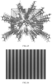
- the present invention provides a Zn-based organically-coordinated nanoparticle, which is a metal-organic one-dimensional repeatedly-arranged chain structure with a structural general formula of [ZnX 2 (CH 3 COO)Y] n , wherein X is selected from benzoate or m-methylbenzoate, Y is selected from organic amine ligands, and n is a degree of polymerization, which is greater than or equal to 1.
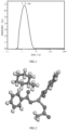
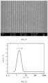
- the size of the prepared Zn-based organically-coordinated nanoparticle is from 1nm to 4 nm.
- the organic amine ligand is selected from N-methylpiperidine, N-methylpyrrolidine, cyclohexylimine, and methylpyrrolidine.
- the present invention also provides a method for preparing a Zn-based organically-coordinated nanoparticle, comprising the following steps:
- the first organic ligand is benzoic acid or m-methylbenzoic acid
- the second organic ligand is selected from N-methylpiperidine, N-methylpyrrolidine, cyclohexylimine, and methylpyrrolidine.
- the molar ratio of the metallic zinc salt, the first organic ligand, and the second organic ligand is (0.2 ⁇ 1):(0.4 ⁇ 1):(0.3 ⁇ 1); preferably, the molar ratio of the metallic zinc salt, the first organic ligand, and the second organic ligand is 1:(3-5):(2-5).
- step (2) the temperature range of the heating and stirring is from 50°C to 80°C, and the period thereof is from 10h to 40h.
- the present invention also provides a Zn-based organically-coordinated nanoparticle obtained by the above-mentioned preparation method.
- the present invention provides a Zn-based organically-coordinated nanoparticle with a chemical formula of [ZnX 2 (CH 3 COO)Y] n , wherein X is a ligand selected from benzoic acid or m-methylbenzoic acid, Y is selected from N-methylpiperidine, N-methylpyrrolidine, cyclohexylimine, methylpyrrolidine, n is a degree of polymerization and is greater than or equal to 1, and as the n value increases, the nanoparticle is a metal-organic one-dimensional repeatedly-arranged chain structure. Further, the size of the nanoparticle is from 1 nm to 4 nm.
- the present invention also provides a method for preparing a Zn-based organically-coordinated nanoparticle, comprising the following steps:
- the molar ratio of the metallic zinc salt, the first organic ligand and the second organic ligand is (0.2 ⁇ 1):(0.4 ⁇ 1):(0.3 ⁇ 1); Further, in the preferred embodiment, the molar ratio of the metallic zinc salt, the first organic ligand and the second organic ligand is within the range of 1:(3 ⁇ 5):(2 ⁇ 5), and a Zn-based organically-coordinated nanoparticle can be obtained.
- step (2) the temperature range of the heating and stirring is from 50°C to 80°C, and the period is from 10h to 40h.
- the temperature is too low, the reaction speed will be too slow.
- the temperature is too high, the reaction will be unstable and a Zn-based organically-coordinated nanoparticle cannot be obtained.
- the vacuum rotary evaporation may be any value between 30 min and 60 min, for example, it may also be 35 min, 40 min, 45 min, 50 min or 55 min.
- the present invention also provides a photoresist composition containing a Zn-based organically-coordinated nanoparticle, which comprises the Zn-based organically-coordinated nanoparticle prepared above, a photoacid agent and an organic dispersing solvent.
- a photoresist composition containing a Zn-based organically-coordinated nanoparticle, which comprises the Zn-based organically-coordinated nanoparticle prepared above, a photoacid agent and an organic dispersing solvent.
- the mass percentage of the Zn-based organically-coordinated nanoparticle is 3%-20%, and the mass percentage of the photoacid agent may be 5%-10%.
- the photoacid agent may be any one or more selected from N-hydroxynaphthalene imide trifluoromethanesulfonic acid, 1,4-aminonaphthalenesulfonic acid, 2-amino-5,7-naphthalene disulfonic acid, tert-butylphenyl iodonium perfluorooctanesulfonic acid, triphenylsulfonium perfluorobutanesulfonic acid, triphenylsulfonium perfluorobutyl and triphenylsulfonium trifluorosulfonic acid.
- the organic dispersing solvent may be any one or more selected from ethyl acetate, butyl acetate, propylene glycol monoethyl ether acetate, propylene glycol methyl ether acetate, 1-ethoxy-2-propanol, methanol, ethanol, and propanol.
- the preparation process of the photoresist composition containing a Zn-based organically-coordinated nanoparticle is to dissolve the obtained nanoparticle with an organic dispersing solvent, then add a photoacid agent thereto, stir the mixture for 5 min until dissolved completely to obtain a mixed photoresist solution.
- An embodiment of the present invention also provides a method for patterning a photoresist, comprising the following steps:
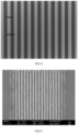
- the exposure condition may be any one selected from Mid-Ultra-Violet, electron beam, and Extreme Ultra-Violet.
- the mask transmissive masks may be used for the light sources of Deep Ultra-Violet and longer wavelength, reflective masks may be used for the light sources of Extreme Ultra-Violet, and electron beam may be used for exposure according to the pattern set by the software.
- the substrate is selected from a silicon sheet, and other substrates insoluble in the developing agent may also be selected according to actual needs.
Landscapes
- Physics & Mathematics (AREA)
- General Physics & Mathematics (AREA)
- Chemical & Material Sciences (AREA)
- Organic Chemistry (AREA)
- Spectroscopy & Molecular Physics (AREA)
- Health & Medical Sciences (AREA)
- Medicinal Chemistry (AREA)
- Chemical Kinetics & Catalysis (AREA)
- Polymers & Plastics (AREA)
- Engineering & Computer Science (AREA)
- Manufacturing & Machinery (AREA)
- Microelectronics & Electronic Packaging (AREA)
- Inorganic Chemistry (AREA)
- Toxicology (AREA)
- Materials For Photolithography (AREA)
- Exposure And Positioning Against Photoresist Photosensitive Materials (AREA)
- Organic Low-Molecular-Weight Compounds And Preparation Thereof (AREA)
Applications Claiming Priority (2)
| Application Number | Priority Date | Filing Date | Title |
|---|---|---|---|
| CN202211050526.1A CN117659420A (zh) | 2022-08-29 | 2022-08-29 | 一种Zn基有机配位纳米颗粒、光刻胶组合物及其制备方法与应用 |
| PCT/CN2023/112964 WO2024046107A1 (zh) | 2022-08-29 | 2023-08-14 | 一种Zn基有机配位纳米颗粒、光刻胶组合物及其制备方法与应用 |
Publications (1)
| Publication Number | Publication Date |
|---|---|
| EP4582467A1 true EP4582467A1 (de) | 2025-07-09 |
Family
ID=90084988
Family Applications (1)
| Application Number | Title | Priority Date | Filing Date |
|---|---|---|---|
| EP23859141.6A Pending EP4582467A1 (de) | 2022-08-29 | 2023-08-14 | Organisch koordinierte nanopartikel auf zn-basis, fotolackzusammensetzung, herstellungsverfahren dafür und verwendung davon |
Country Status (6)
| Country | Link |
|---|---|
| US (1) | US20260044072A1 (de) |
| EP (1) | EP4582467A1 (de) |
| JP (1) | JP2025525925A (de) |
| KR (1) | KR20250029950A (de) |
| CN (1) | CN117659420A (de) |
| WO (1) | WO2024046107A1 (de) |
Families Citing this family (1)
| Publication number | Priority date | Publication date | Assignee | Title |
|---|---|---|---|---|
| CN117659421A (zh) * | 2022-08-29 | 2024-03-08 | 清华大学 | 一种Zn基有机配位纳米颗粒及其制备方法、光刻胶组合物及其应用 |
Family Cites Families (12)
| Publication number | Priority date | Publication date | Assignee | Title |
|---|---|---|---|---|
| WO2009120169A1 (en) | 2008-03-27 | 2009-10-01 | State Of Oregon Acting By And Through The State Board Of Higher Education On Behalf Of Oregon State University | Solution processed thin films and laminates, devices comprising such thin films and laminates, and method for the use and manufacture |
| JP5708518B2 (ja) * | 2011-02-09 | 2015-04-30 | 信越化学工業株式会社 | レジスト材料及びこれを用いたパターン形成方法 |
| KR20140023717A (ko) * | 2012-08-17 | 2014-02-27 | 주식회사 엘지화학 | 광경화성 및 열경화성을 갖는 수지 조성물과 및 이를 사용하여 제조된 드라이 필름 솔더 레지스트 |
| CN104829487B (zh) * | 2015-03-27 | 2016-09-07 | 福州大学 | 聚集发光增强的氨敏金属-有机凝胶复合软材料及其制备 |
| KR102634520B1 (ko) | 2017-11-20 | 2024-02-06 | 인프리아 코포레이션 | 유기주석 클러스터, 유기주석 클러스터의 용액, 및 고해상도 패턴화에 대한 적용 |
| US20190258161A1 (en) * | 2018-02-22 | 2019-08-22 | Jsr Corporation | Radiation-sensitive composition and pattern-forming method |
| TWI875109B (zh) | 2018-04-05 | 2025-03-01 | 美商英培雅股份有限公司 | 包含錫化合物的組合物及其應用 |
| US12153347B2 (en) * | 2018-06-29 | 2024-11-26 | National Institute Of Advanced Industrial Science And Technology | Organically modified metal oxide nanoparticle, method for producing the same, EUV photoresist material, and method for producing etching mask |
| WO2021016229A1 (en) | 2019-07-22 | 2021-01-28 | Inpria Corporation | Organometallic metal chalcogenide clusters and application to lithography |
| US11934101B2 (en) * | 2019-11-27 | 2024-03-19 | Taiwan Semiconductor Manufacturing Company, Ltd. | Photoresist composition and method of forming photoresist pattern |
| CN112462572B (zh) * | 2020-12-09 | 2022-08-16 | 清华大学 | 光刻胶、光刻胶的图案化方法及生成印刷电路板的方法 |
| CN114675488B (zh) * | 2020-12-24 | 2025-07-25 | 清华大学 | 锌基金属有机纳米颗粒及其制备方法以及光刻胶 |
-
2022
- 2022-08-29 CN CN202211050526.1A patent/CN117659420A/zh active Pending
-
2023
- 2023-08-14 EP EP23859141.6A patent/EP4582467A1/de active Pending
- 2023-08-14 US US18/995,887 patent/US20260044072A1/en active Pending
- 2023-08-14 WO PCT/CN2023/112964 patent/WO2024046107A1/zh not_active Ceased
- 2023-08-14 JP JP2025506044A patent/JP2025525925A/ja active Pending
- 2023-08-14 KR KR1020257003454A patent/KR20250029950A/ko active Pending
Also Published As
| Publication number | Publication date |
|---|---|
| WO2024046107A1 (zh) | 2024-03-07 |
| KR20250029950A (ko) | 2025-03-05 |
| JP2025525925A (ja) | 2025-08-07 |
| CN117659420A (zh) | 2024-03-08 |
| US20260044072A1 (en) | 2026-02-12 |
Similar Documents
| Publication | Publication Date | Title |
|---|---|---|
| JP7578231B2 (ja) | 亜鉛系有機金属ナノ粒子及びその製造方法、並びにフォトレジスト | |
| Si et al. | A novel stable zinc–oxo cluster for advanced lithography patterning | |
| Krysak et al. | Development of an inorganic nanoparticle photoresist for EUV, e-beam, and 193nm lithography | |
| JP7667928B2 (ja) | チタンジルコニウム酸化物ナノ粒子、フォトレジスト、フォトレジストのパターニング方法及びプリント回路基板を生成する方法 | |
| CN111965947B (zh) | 光刻胶、光刻胶的图案化方法及集成电路板的刻蚀方法 | |
| TWI788560B (zh) | 鋶鹽、光酸產生劑、能量線硬化性組成物、硬化體、化學增幅型正型光阻組成物、抗蝕劑圖案之製作方法及化學增幅型負型光阻組成物 | |
| WO2023085414A1 (ja) | 多環芳香族炭化水素系光硬化性樹脂組成物 | |
| JP4551510B2 (ja) | 色素含有感光性耐食膜および方法ならびにこれを含む工業製品 | |
| EP4582467A1 (de) | Organisch koordinierte nanopartikel auf zn-basis, fotolackzusammensetzung, herstellungsverfahren dafür und verwendung davon | |
| Chen et al. | Hybrid alkyl-ligand tin-oxo clusters for enhanced lithographic patterning performance via intramolecular interactions | |
| JP6046540B2 (ja) | スルホニウム塩、光酸発生剤、硬化性組成物およびレジスト組成物 | |
| CN113651357A (zh) | 锆氧化物纳米粒子及其制备方法、光刻胶组合物及其应用 | |
| CN111538211A (zh) | 一种酚醛树脂光刻胶组合物及其制备方法 | |
| EP4582431A1 (de) | Organische koordinationsnanopartikel auf zn-basis und herstellungsverfahren dafür, fotolackzusammensetzung damit und verwendung davon | |
| JP2025528818A (ja) | Co系有機配位ナノ粒子及びその製造方法、フォトレジスト組成物及びその使用 | |
| CN114089599A (zh) | 基于金属纳米颗粒的光刻胶组合物及其应用 | |
| EP4582870A1 (de) | Organische koordinationsnanopartikel auf zn-basis und herstellungsverfahren dafür, fotolackzusammensetzung und verwendung davon | |
| WO2025050877A1 (zh) | 一种Ni基有机配位纳米颗粒及其制备方法、包含其的光刻胶组合物及其应用 | |
| JP2025527067A (ja) | Ag系有機配位ナノ粒子、その製造方法、フォトレジスト組成物及びその使用 | |
| CN120665221A (zh) | 含邻硝基苄醚和重氮萘醌双光敏基团的感光分子、光刻胶组合物、制备方法及光刻方法 | |
| CN118994209A (zh) | 一种“全同结构”锌基杂化化合物及其制备方法和在光刻胶中的应用 | |
| JPH0480757A (ja) | パターン形成方法 |
Legal Events
| Date | Code | Title | Description |
|---|---|---|---|
| STAA | Information on the status of an ep patent application or granted ep patent |
Free format text: STATUS: THE INTERNATIONAL PUBLICATION HAS BEEN MADE |
|
| PUAI | Public reference made under article 153(3) epc to a published international application that has entered the european phase |
Free format text: ORIGINAL CODE: 0009012 |
|
| STAA | Information on the status of an ep patent application or granted ep patent |
Free format text: STATUS: REQUEST FOR EXAMINATION WAS MADE |
|
| 17P | Request for examination filed |
Effective date: 20250228 |
|
| AK | Designated contracting states |
Kind code of ref document: A1 Designated state(s): AL AT BE BG CH CY CZ DE DK EE ES FI FR GB GR HR HU IE IS IT LI LT LU LV MC ME MK MT NL NO PL PT RO RS SE SI SK SM TR |
|
| DAV | Request for validation of the european patent (deleted) | ||
| DAX | Request for extension of the european patent (deleted) |