EP4579718A1 - Verfahren zur substratverarbeitung, verfahren zur herstellung eines halbleiterbauelements, programm und substratverarbeitungsvorrichtung - Google Patents
Verfahren zur substratverarbeitung, verfahren zur herstellung eines halbleiterbauelements, programm und substratverarbeitungsvorrichtung Download PDFInfo
- Publication number
- EP4579718A1 EP4579718A1 EP24222793.2A EP24222793A EP4579718A1 EP 4579718 A1 EP4579718 A1 EP 4579718A1 EP 24222793 A EP24222793 A EP 24222793A EP 4579718 A1 EP4579718 A1 EP 4579718A1
- Authority
- EP
- European Patent Office
- Prior art keywords
- film
- recess
- sacrificial
- precursor
- dielectric film
- Prior art date
- Legal status (The legal status is an assumption and is not a legal conclusion. Google has not performed a legal analysis and makes no representation as to the accuracy of the status listed.)
- Pending
Links
Images



Classifications
-
- H—ELECTRICITY
- H10—SEMICONDUCTOR DEVICES; ELECTRIC SOLID-STATE DEVICES NOT OTHERWISE PROVIDED FOR
- H10P—GENERIC PROCESSES OR APPARATUS FOR THE MANUFACTURE OR TREATMENT OF DEVICES COVERED BY CLASS H10
- H10P14/00—Formation of materials, e.g. in the shape of layers or pillars
- H10P14/60—Formation of materials, e.g. in the shape of layers or pillars of insulating materials
- H10P14/69—Inorganic materials
- H10P14/692—Inorganic materials composed of oxides, glassy oxides or oxide-based glasses
- H10P14/6921—Inorganic materials composed of oxides, glassy oxides or oxide-based glasses containing silicon
- H10P14/6922—Inorganic materials composed of oxides, glassy oxides or oxide-based glasses containing silicon the material containing Si, O and at least one of H, N, C, F or other non-metal elements, e.g. SiOC, SiOC:H or SiONC
- H10P14/6927—Inorganic materials composed of oxides, glassy oxides or oxide-based glasses containing silicon the material containing Si, O and at least one of H, N, C, F or other non-metal elements, e.g. SiOC, SiOC:H or SiONC the material being a silicon oxynitride, e.g. SiON or SiON:H
-
- H—ELECTRICITY
- H10—SEMICONDUCTOR DEVICES; ELECTRIC SOLID-STATE DEVICES NOT OTHERWISE PROVIDED FOR
- H10P—GENERIC PROCESSES OR APPARATUS FOR THE MANUFACTURE OR TREATMENT OF DEVICES COVERED BY CLASS H10
- H10P14/00—Formation of materials, e.g. in the shape of layers or pillars
- H10P14/60—Formation of materials, e.g. in the shape of layers or pillars of insulating materials
- H10P14/61—Formation of materials, e.g. in the shape of layers or pillars of insulating materials using masks
-
- H—ELECTRICITY
- H10—SEMICONDUCTOR DEVICES; ELECTRIC SOLID-STATE DEVICES NOT OTHERWISE PROVIDED FOR
- H10P—GENERIC PROCESSES OR APPARATUS FOR THE MANUFACTURE OR TREATMENT OF DEVICES COVERED BY CLASS H10
- H10P14/00—Formation of materials, e.g. in the shape of layers or pillars
- H10P14/60—Formation of materials, e.g. in the shape of layers or pillars of insulating materials
- H10P14/63—Formation of materials, e.g. in the shape of layers or pillars of insulating materials characterised by the formation processes
- H10P14/6326—Deposition processes
- H10P14/6328—Deposition from the gas or vapour phase
-
- C—CHEMISTRY; METALLURGY
- C23—COATING METALLIC MATERIAL; COATING MATERIAL WITH METALLIC MATERIAL; CHEMICAL SURFACE TREATMENT; DIFFUSION TREATMENT OF METALLIC MATERIAL; COATING BY VACUUM EVAPORATION, BY SPUTTERING, BY ION IMPLANTATION OR BY CHEMICAL VAPOUR DEPOSITION, IN GENERAL; INHIBITING CORROSION OF METALLIC MATERIAL OR INCRUSTATION IN GENERAL
- C23C—COATING METALLIC MATERIAL; COATING MATERIAL WITH METALLIC MATERIAL; SURFACE TREATMENT OF METALLIC MATERIAL BY DIFFUSION INTO THE SURFACE, BY CHEMICAL CONVERSION OR SUBSTITUTION; COATING BY VACUUM EVAPORATION, BY SPUTTERING, BY ION IMPLANTATION OR BY CHEMICAL VAPOUR DEPOSITION, IN GENERAL
- C23C16/00—Chemical coating by decomposition of gaseous compounds, without leaving reaction products of surface material in the coating, i.e. chemical vapour deposition [CVD] processes
- C23C16/04—Coating on selected surface areas, e.g. using masks
-
- C—CHEMISTRY; METALLURGY
- C23—COATING METALLIC MATERIAL; COATING MATERIAL WITH METALLIC MATERIAL; CHEMICAL SURFACE TREATMENT; DIFFUSION TREATMENT OF METALLIC MATERIAL; COATING BY VACUUM EVAPORATION, BY SPUTTERING, BY ION IMPLANTATION OR BY CHEMICAL VAPOUR DEPOSITION, IN GENERAL; INHIBITING CORROSION OF METALLIC MATERIAL OR INCRUSTATION IN GENERAL
- C23C—COATING METALLIC MATERIAL; COATING MATERIAL WITH METALLIC MATERIAL; SURFACE TREATMENT OF METALLIC MATERIAL BY DIFFUSION INTO THE SURFACE, BY CHEMICAL CONVERSION OR SUBSTITUTION; COATING BY VACUUM EVAPORATION, BY SPUTTERING, BY ION IMPLANTATION OR BY CHEMICAL VAPOUR DEPOSITION, IN GENERAL
- C23C16/00—Chemical coating by decomposition of gaseous compounds, without leaving reaction products of surface material in the coating, i.e. chemical vapour deposition [CVD] processes
- C23C16/44—Chemical coating by decomposition of gaseous compounds, without leaving reaction products of surface material in the coating, i.e. chemical vapour deposition [CVD] processes characterised by the method of coating
- C23C16/455—Chemical coating by decomposition of gaseous compounds, without leaving reaction products of surface material in the coating, i.e. chemical vapour deposition [CVD] processes characterised by the method of coating characterised by the method used for introducing gases into reaction chamber or for modifying gas flows in reaction chamber
-
- C—CHEMISTRY; METALLURGY
- C23—COATING METALLIC MATERIAL; COATING MATERIAL WITH METALLIC MATERIAL; CHEMICAL SURFACE TREATMENT; DIFFUSION TREATMENT OF METALLIC MATERIAL; COATING BY VACUUM EVAPORATION, BY SPUTTERING, BY ION IMPLANTATION OR BY CHEMICAL VAPOUR DEPOSITION, IN GENERAL; INHIBITING CORROSION OF METALLIC MATERIAL OR INCRUSTATION IN GENERAL
- C23C—COATING METALLIC MATERIAL; COATING MATERIAL WITH METALLIC MATERIAL; SURFACE TREATMENT OF METALLIC MATERIAL BY DIFFUSION INTO THE SURFACE, BY CHEMICAL CONVERSION OR SUBSTITUTION; COATING BY VACUUM EVAPORATION, BY SPUTTERING, BY ION IMPLANTATION OR BY CHEMICAL VAPOUR DEPOSITION, IN GENERAL
- C23C16/00—Chemical coating by decomposition of gaseous compounds, without leaving reaction products of surface material in the coating, i.e. chemical vapour deposition [CVD] processes
- C23C16/44—Chemical coating by decomposition of gaseous compounds, without leaving reaction products of surface material in the coating, i.e. chemical vapour deposition [CVD] processes characterised by the method of coating
- C23C16/52—Controlling or regulating the coating process
-
- H—ELECTRICITY
- H10—SEMICONDUCTOR DEVICES; ELECTRIC SOLID-STATE DEVICES NOT OTHERWISE PROVIDED FOR
- H10B—ELECTRONIC MEMORY DEVICES
- H10B43/00—EEPROM devices comprising charge-trapping gate insulators
- H10B43/20—EEPROM devices comprising charge-trapping gate insulators characterised by three-dimensional [3D] arrangements, e.g. with cells on different height levels
- H10B43/23—EEPROM devices comprising charge-trapping gate insulators characterised by three-dimensional [3D] arrangements, e.g. with cells on different height levels with source and drain on different levels, e.g. with sloping channels
- H10B43/27—EEPROM devices comprising charge-trapping gate insulators characterised by three-dimensional [3D] arrangements, e.g. with cells on different height levels with source and drain on different levels, e.g. with sloping channels the channels comprising vertical portions, e.g. U-shaped channels
-
- H—ELECTRICITY
- H10—SEMICONDUCTOR DEVICES; ELECTRIC SOLID-STATE DEVICES NOT OTHERWISE PROVIDED FOR
- H10P—GENERIC PROCESSES OR APPARATUS FOR THE MANUFACTURE OR TREATMENT OF DEVICES COVERED BY CLASS H10
- H10P14/00—Formation of materials, e.g. in the shape of layers or pillars
- H10P14/60—Formation of materials, e.g. in the shape of layers or pillars of insulating materials
-
- H—ELECTRICITY
- H10—SEMICONDUCTOR DEVICES; ELECTRIC SOLID-STATE DEVICES NOT OTHERWISE PROVIDED FOR
- H10P—GENERIC PROCESSES OR APPARATUS FOR THE MANUFACTURE OR TREATMENT OF DEVICES COVERED BY CLASS H10
- H10P14/00—Formation of materials, e.g. in the shape of layers or pillars
- H10P14/60—Formation of materials, e.g. in the shape of layers or pillars of insulating materials
- H10P14/63—Formation of materials, e.g. in the shape of layers or pillars of insulating materials characterised by the formation processes
- H10P14/6326—Deposition processes
- H10P14/6328—Deposition from the gas or vapour phase
- H10P14/6334—Deposition from the gas or vapour phase using decomposition or reaction of gaseous or vapour phase compounds, i.e. chemical vapour deposition
-
- H—ELECTRICITY
- H10—SEMICONDUCTOR DEVICES; ELECTRIC SOLID-STATE DEVICES NOT OTHERWISE PROVIDED FOR
- H10P—GENERIC PROCESSES OR APPARATUS FOR THE MANUFACTURE OR TREATMENT OF DEVICES COVERED BY CLASS H10
- H10P14/00—Formation of materials, e.g. in the shape of layers or pillars
- H10P14/60—Formation of materials, e.g. in the shape of layers or pillars of insulating materials
- H10P14/65—Formation of materials, e.g. in the shape of layers or pillars of insulating materials characterised by treatments performed before or after the formation of the materials
- H10P14/6516—Formation of materials, e.g. in the shape of layers or pillars of insulating materials characterised by treatments performed before or after the formation of the materials of treatments performed after formation of the materials
- H10P14/6529—Formation of materials, e.g. in the shape of layers or pillars of insulating materials characterised by treatments performed before or after the formation of the materials of treatments performed after formation of the materials by exposure to a gas or vapour
-
- H—ELECTRICITY
- H10—SEMICONDUCTOR DEVICES; ELECTRIC SOLID-STATE DEVICES NOT OTHERWISE PROVIDED FOR
- H10P—GENERIC PROCESSES OR APPARATUS FOR THE MANUFACTURE OR TREATMENT OF DEVICES COVERED BY CLASS H10
- H10P14/00—Formation of materials, e.g. in the shape of layers or pillars
- H10P14/60—Formation of materials, e.g. in the shape of layers or pillars of insulating materials
- H10P14/65—Formation of materials, e.g. in the shape of layers or pillars of insulating materials characterised by treatments performed before or after the formation of the materials
- H10P14/6516—Formation of materials, e.g. in the shape of layers or pillars of insulating materials characterised by treatments performed before or after the formation of the materials of treatments performed after formation of the materials
- H10P14/6548—Formation of materials, e.g. in the shape of layers or pillars of insulating materials characterised by treatments performed before or after the formation of the materials of treatments performed after formation of the materials by forming intermediate materials, e.g. capping layers or diffusion barriers
-
- H—ELECTRICITY
- H10—SEMICONDUCTOR DEVICES; ELECTRIC SOLID-STATE DEVICES NOT OTHERWISE PROVIDED FOR
- H10P—GENERIC PROCESSES OR APPARATUS FOR THE MANUFACTURE OR TREATMENT OF DEVICES COVERED BY CLASS H10
- H10P14/00—Formation of materials, e.g. in the shape of layers or pillars
- H10P14/60—Formation of materials, e.g. in the shape of layers or pillars of insulating materials
- H10P14/69—Inorganic materials
- H10P14/692—Inorganic materials composed of oxides, glassy oxides or oxide-based glasses
- H10P14/6921—Inorganic materials composed of oxides, glassy oxides or oxide-based glasses containing silicon
- H10P14/69215—Inorganic materials composed of oxides, glassy oxides or oxide-based glasses containing silicon the material being a silicon oxide, e.g. SiO2
-
- H—ELECTRICITY
- H10—SEMICONDUCTOR DEVICES; ELECTRIC SOLID-STATE DEVICES NOT OTHERWISE PROVIDED FOR
- H10P—GENERIC PROCESSES OR APPARATUS FOR THE MANUFACTURE OR TREATMENT OF DEVICES COVERED BY CLASS H10
- H10P14/00—Formation of materials, e.g. in the shape of layers or pillars
- H10P14/60—Formation of materials, e.g. in the shape of layers or pillars of insulating materials
- H10P14/69—Inorganic materials
- H10P14/694—Inorganic materials composed of nitrides
- H10P14/6943—Inorganic materials composed of nitrides containing silicon
- H10P14/69433—Inorganic materials composed of nitrides containing silicon the material being a silicon nitride not containing oxygen, e.g. SixNy or SixByNz
Definitions
- the present disclosure relates to a method of processing a substrate, a method of manufacturing a semiconductor device, a program, and a substrate processing apparatus.
- Some embodiments of the present disclosure provide a technique capable of precisely forming a film on a substrate.
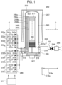
- a process furnace 202 of a substrate processing apparatus includes a reaction tube 203.
- a manifold 209 is installed below the reaction tube 203.
- a process container mainly includes the reaction tube 203 and the manifold 209.
- a process chamber 201 is formed inside the process container.
- the process chamber 201 is configured to be capable of accommodating wafers 200 as substrates.
- a heater 207 configured to heat the wafers 200 in the process chamber 201 is installed outside the reaction tube 203.
- the heater 207 also functions as an activator configured to thermally activate a gas in the process chamber 201.
- a temperature sensor 263 is installed inside the reaction tube 203.
- a first precursor is supplied from the gas supply pipe 232a into the process chamber 201 via the MFC 241a, the valve 243a, and the nozzle 249a.
- Reactants (an oxidizing agent and a nitriding agent) are supplied from the gas supply pipe 232b into the process chamber 201 via the MFC 241b, the valve 243b, and the nozzle 249b.
- a second precursor is supplied from the gas supply pipe 232d into the process chamber 201 via the MFC 241d, the valve 243d, the gas supply pipe 232a, and the nozzle 249a.
- a third precursor is supplied from the gas supply pipe 232e into the process chamber 201 via the MFC 241e, the valve 243e, the gas supply pipe 232a, and the nozzle 249a.
- An inert gas is supplied from the gas supply pipes 232g to 232i into the process chamber 201 via the MFCs 241g to 241i, the valves 243g to 243i, the gas supply pipes 232a to 232c, and the nozzles 249a to 249c.
- the inert gas acts as a purge gas, a carrier gas, a dilution gas, or the like.
- a first precursor supply system mainly includes the gas supply pipe 232a, the MFC 241a, and the valve 243a.
- a reactant (an oxidizing agent and a nitriding agent) supply system mainly includes the gas supply pipe 232b, the MFC 241b, and the valve 243b.
- a modifying agent supply system mainly includes the gas supply pipe 232c, the MFC 241c, and the valve 243c.
- a second precursor supply system mainly includes the gas supply pipe 232d, the MFC 241d, and the valve 243d.
- a third precursor supply system mainly includes the gas supply pipe 232e, the MFC 241e, and the valve 243e.
- a catalyst supply system mainly includes the gas supply pipe 232f, the MFC 241f, and the valve 243f.
- An inert gas supply system mainly includes the gas supply pipes 232g to 232i, the MFCs 241g to 241i, and the valves 243g to 243i. Any one or the entirety of the above-described various supply systems may be constituted as an integrated supply system 248 in which the valves 243a to 243i, the MFCs 241a to 241i, and so on are integrated.
- a reactant supply system configured to supply the reactant to the nozzle 249c is installed for each of the different reactants.
- An exhaust port 231a is installed below the reaction tube 203.
- a vacuum pump 246 is connected to the exhaust pipe 231 via a pressure sensor 245 and an auto pressure controller (APC) valve 244.
- An exhaust system mainly includes the exhaust pipe 231, the APC valve 244, and the pressure sensor 245.
- the vacuum pump 246 may be included in the exhaust system.
- a seal cap 219 is installed below the manifold 209.
- a rotator 267 configured to rotate a boat 217 to described below is provided at the seal cap 219.
- the seal cap 219 is raised or lowered by a boat elevator 115.
- the boat elevator 115 functions as a transporter configured to transport the wafers 200 into or out of the process chamber 201.
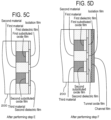
- a recess is formed on the surface of the wafer 200 with the first sacrificial film and the second sacrificial film as sidewalls, and the surface of the second material as a bottom.
- steps B1 and B2 are performed on the wafer 200 after the first sacrificial film and the second sacrificial film are formed on the surface of the wafer 200.
- the following steps are performed on the wafer 200.
- an oxidizing agent may be used as the reactant.
- a catalyst may be supplied to the wafer 200. The following describes a case where a catalyst is supplied in both the steps of supplying the second precursor and the step of supplying the reactant.
- valves 243d and 243f are opened to supply the second precursor and the catalyst to the wafer 200.
- the valves 243g to 243i may be opened to supply an inert gas into the process chamber 201.
- a second precursor adsorption layer in the recess with the first and second sacrificial films as sidewalls and on at least a portion of an upper surface of each of the first and second sacrificial films.
- the second precursor adsorption layer contains at least a portion of a molecular structure of a molecule constituting the second precursor.
- valves 243d and 243f are closed to stop the supply of second precursor and the supply of catalyst to the wafer 200. Then, according to the above-described sequence, gaseous substances and the like remaining in the process chamber 201 are removed from the inside of the process chamber 201, and the inside of the process chamber 201 is purged with an inert gas (purging).
- valves 243b and 243f are opened to supply a reactant and a catalyst to the wafer 200.
- the valves 243g to 243i may be opened to supply an inert gas into the process chamber 201.
- the second precursor adsorption layer formed in the recess with the first and second sacrificial films as sidewalls and the second precursor adsorption layer formed on at least a portion of the upper surface of each of the first and second sacrificial films may be modified respectively.
- the second precursor adsorption layer may be oxidized to form an oxide layer containing a constituent element of the second precursor in the recess with the first and second sacrificial films as sidewalls and on at least a portion of the upper surface of each of the first and second sacrificial films.
- valves 243b and 243f are closed to stop the supply of reactant and the catalyst to the wafer 200. Then, by the above-described procedure, gaseous substances and the like remaining in the process chamber 201 are removed from the inside of the process chamber 201, and the process chamber 201 is purged with an inert gas.
- a cycle including supply of the second precursor and supply of the reactant is performed a predetermined number of times (n B times where n B is an integer of 1 or 2 or more).
- n B is an integer of 1 or 2 or more.
- a filling film may be formed in the recess with the first sacrificial film and the second sacrificial film as sidewalls, and on at least a portion of the upper surface of each of the first sacrificial film and the second sacrificial film.
- This cycle is performed until the recess is filled with the filling film.
- an oxide film for example, a silicon oxide film (SiO film) may be formed as the filling film.
- the second precursor may be, for example, the above-described Si-containing substances such as alkylaminosilane, aminosilane, chlorosilane, and the like. As the second precursor, one or more of these substances may be used.
- the reactant (oxidizing agent) may be, for example, oxygen (O 2 ), ozone (O 3 ), water vapor (H 2 O), nitrous oxide (N 2 O), nitric oxide (NO), nitrogen dioxide (NO 2 ), carbon dioxide (CO 2 ), carbon monoxide (CO), or the like.
- oxygen (O) oxygen
- ozone (O 3 ) water vapor
- N 2 O nitrous oxide
- NO nitric oxide
- NO 2 nitrogen dioxide
- CO 2 carbon monoxide
- a reactant with a relatively weak oxidizing power may be used to suppress the first sacrificial film and the second sacrificial film from being substantially modified (oxidized) into an oxide film by the reactant.
- a reactant with a weaker oxidizing power than the oxidizing agent used in step E to be described below may be used.
- an oxidizing agent with a relatively strong oxidizing power exemplified in step E to be described below may also be used.
- the catalyst may be, for example, pyridine (C 5 H 5 N), picoline (C 6 H 7 N), lutidine (C 7 H 9 N), triethylamine ((C 2 H 5 ) 3 N), or the like. As the catalyst, one or more of these amines may be used.
- the inside of the process chamber 201 is purged, and gases and reaction by-products remaining in the process chamber 201 are removed from the inside of the process chamber 201 (after-purge). Thereafter, an internal atmosphere of the process chamber 201 is replaced with an inert gas (replacement of inert gas), and the internal pressure of the process chamber 201 is returned to the atmospheric pressure (returning to atmospheric pressure). Then, the processed wafers 200 are unloaded to the outside of the reaction tube 203 (boat unloading) and discharged from the boat 217 (wafer discharging). After the boat unloading, the lower end opening of the manifold 209 is sealed by the shutter 219s (shutter closing).
- step B2 is performed on the wafer 200 after the wafer discharging, i.e., the wafer 200 after the filling film is formed on the surface of the wafer 200.
- step B2 a portion of the filling film formed in the recess formed on the surface of the wafer 200 is left as an isolation film, and other portions of the filling film are removed to expose at least portions of the first sacrificial film and the second sacrificial film.
- a partial removal of the filling film may be performed by an anisotropic etching in which for example, a plasma-excited etching gas such as a fluorocarbon (CF)-based gas is used.
- the anisotropic etching may be performed, for example, by using a first etching unit as a plasma etching apparatus, according to a known processing sequence and processing conditions.
- the CF-based gas for example, one or more selected from the group of a CF 4 gas, a C 4 F 6 gas, a C 4 F 8 gas, a CH 2 F 2 gas, a CHF 3 gas, and the like may be used.
- the partial removal of the filling film is not limited to the case of being performed by anisotropic etching.
- the partial removal of the filling film may also be performed by, for example, a chemical mechanical polishing (CMP).
- the surface of the wafer 200 is in a state where the first sacrificial film, the isolation film, and the second sacrificial film, which are adjacent to one another sequentially, are exposed.
- the first sacrificial film and the second sacrificial film are physically isolated (separated) with the isolation film interposed therebetween.
- the partial removal of the filling film is performed by anisotropic etching or CMP as described above, it is possible to allow the entire exposed surfaces of the first sacrificial film, the isolation film, and the second sacrificial film to become smooth surfaces (flat surfaces or curved surfaces) adjacent to one another without any steps.
- the first sacrificial film and the second sacrificial film may be selectively removed with respect to the isolation film, the first material, and the third material.
- the isolation film constituting the side surfaces of these recesses may also be suitably used as an isolator (separator) that physically and electrically isolates the films formed inside the recesses.
- the following steps are performed on the wafer 200.
- an oxidizing agent may be used as the reactant.
- valve 243e is opened to supply a third precursor to the wafer 200.
- the valves 243g to 243i may be opened to supply an inert gas into the process chamber 201.
- the supply of third precursor under processing conditions to be described below, it is possible to form a third precursor adsorption layer in the first and second recesses formed on the surface of the wafer 200 and on at least a portion of the upper surface of the isolation film formed on the surface of the wafer 200.
- the third precursor adsorption layer contains at least a portion of a molecular structure of a molecule constituting the third precursor.
- valve 243b is opened to supply a reactant to the wafer 200.
- the valves 243g to 243i may be opened to supply an inert gas into the process chamber 201.
- the third precursor adsorption layer formed in the first and second recesses By performing this step (the supply of reactant) under processing conditions to be described below, it is possible to modify the third precursor adsorption layer formed in the first and second recesses, and the third precursor adsorption layer formed on at least a portion of the upper surface of the isolation film formed on the surface of the wafer 200, respectively.
- the third precursor adsorption layer When an oxidizing agent is used as the reactant, the third precursor adsorption layer may be oxidized, and an oxide layer containing a constituent element of the third precursor may be formed in the first and second recesses and on at least a portion of the upper surface of the isolation film formed on the surface of the wafer 200.
- valve 243b is closed to stop the supply of reactant to the wafer 200. Then, by the above-described sequence, gaseous substances and the like remaining in the process chamber 201 are removed from the inside of the process chamber 201, and the inside of the process chamber 201 is purged with an inert gas.
- a cycle including: the supply of third precursor; and the supply of reactant is performed a predetermined number of times (n D times where no is an integer of 1 or 2 or more).
- n D times where no is an integer of 1 or 2 or more.
- this film becomes a dielectric film which is an oxide film such as an aluminum oxide film (AlO film), a titanium oxide film (TiO film), a hafnium oxide film (HfO film), a zirconium oxide film (ZrO film) or the like, i.e., a metal oxide film with a higher electron trap density than a SiN film.
- the dielectric film in the present disclosure is not limited to the oxide film, and a nitride film containing a similar metal element may also be used as the dielectric film. However, when step E to be described below is further performed, the oxide film may be used as the dielectric film.
- the third precursor may be, for example, aluminum trichloride (AlCl 3 ), trimethylaluminum (Al(CH 3 ) 3 ), titanium tetrachloride (TiCl 4 ), hafnium tetrafluoride (HfF 4 ), tetrakisethylmethylaminohafnium (Hf[N(CH 3 )(CH 2 CH 3 )] 4 ), zirconium tetrafluoride (ZrF 4 ), tetrakisethylmethylaminozirconium (Zr[N(CH 3 )Cp] 4 ), or the like.
- AlCl 3 aluminum trichloride
- Al(CH 3 ) 3 trimethylaluminum
- TiCl 4 titanium tetrachloride
- HfF 4 hafnium tetrafluoride
- ZrF 4 zirconium tetrafluoride
- ZrF 4 tetra
- one or more selected from the group of these substances i.e., substances containing metal elements such as aluminum (Al), titanium (Ti), hafnium (Hf), zirconium (Zr), and the like (organic metals or metal halides) may be used.
- metal elements such as aluminum (Al), titanium (Ti), hafnium (Hf), zirconium (Zr), and the like (organic metals or metal halides) may be used.
- reactant oxidizing agent
- one or more of the O-containing substances described above may be used.
- the other processing conditions may be the same as those used when supplying the third precursor.
- the reactant may be a nitriding agent.
- the reactant may be one or more of the above-described N-containing substances.
- a Si-containing substance is used as the third precursor and a nitriding agent is used as the reactant, a SiN film may be formed as the dielectric film.
- step D1 the above-described unloading sequence (from after-purge to wafer discharging) is performed again, and the wafers 200 with the dielectric film formed on their surfaces are unloaded from the process chamber 201 and discharged from the boat 217.
- step D2 is performed on the wafer 200 after the wafer discharging, i.e., the wafer 200 as an intermediate product after the dielectric film is formed on the surface of the wafer 200 by performing step D1.
- step D2 portions of the dielectric film formed on the surface of the wafer 200 that fill the first and second recesses are left as a first dielectric film and a second dielectric film, respectively, and the remaining portions of the dielectric film are removed.
- a partial removal of the dielectric film may be performed by various methods exemplified in step B2, such as anisotropic etching by a plasma-excited CF-based gas, CMP, and the like. These methods may be performed, for example, by using a first etching unit as a plasma etching apparatus.
- the surface of the wafer 200 is in a state in which the first dielectric film, the isolation film, and the second dielectric film, which are adjacent to one another sequentially, are exposed.
- the first dielectric film and the second dielectric film are physically and electrically isolated (separated) with the isolation film interposed therebetween.
- anisotropic etching or CMP as described above, it is possible to allow the entire exposed surfaces of the first dielectric film, the isolation film, and the second dielectric film to become smooth surfaces (flat surfaces or curved surfaces) adjacent to one another without any steps.
- An electron trap density of each of the first dielectric film and the second dielectric film made of a metal oxide film such as an AlO film or the like is larger than that of a SiN film with the same film thickness.
- step C by forming the first recess so as to protrude toward the surface of the second material beyond the boundary between the surface of the second material and the surface of the first material, it is possible to form the first dielectric film so as to protrude toward the surface of the second material beyond the boundary in step D2. Further, in step C, by forming the second recess so as to protrude toward the surface of the second material beyond the boundary between the surface of the second material and the surface of the third material, it is possible to form the second dielectric film so as to protrude toward the surface of the second material beyond the boundary in step D2.
- step E is performed on the wafer 200 after the first dielectric film and the second dielectric film are formed on the surface of the wafer 200.
- Step E is started after the above-described loading sequence (from wafer charging and boat loading to pressure regulation and temperature regulation) is performed again, the wafer 200 as an intermediate product obtained by performing steps A to D2 is loaded into the process chamber 201 again, and the pressure regulation and temperature regulation in the process chamber 201 are completed.
- valve 243b is opened to supply a reactant containing oxygen (i.e., an oxidizing agent) to the wafer 200.
- a reactant containing oxygen i.e., an oxidizing agent
- the valves 243g to 243i may be opened to supply an inert gas into the process chamber 201.
- a portion of the first material in contact with the interface between the first material and the first dielectric film through the first dielectric film may be modified (oxidized) into a first substituted oxide film
- a portion of the third material in contact with the interface between the third material and the second dielectric film through the second dielectric film can be modified (oxidized) into a second substituted oxide film.
- the first substituted oxide film and the second substituted oxide film are constituted as, for example, a SiO film or a SiON film.
- step E it is possible to further improve characteristics of the isolation film, the first dielectric film, and the second dielectric film as the oxide film without impairing the characteristics of the isolation film, the first dielectric film, and the second dielectric film. For example, it is possible to re-oxidize (additionally oxidize) the isolation film, the first dielectric film, and the second dielectric film, to desorb impurities from these films, densify these films, and improve insulating properties of these films.
- valve 243b is closed to stop the supply of oxidizing agent into the process chamber 201. Then, by the above-described sequence, gaseous substances and the like remaining in the process chamber 201 are removed from the inside of the process chamber 201, and the inside of the process chamber 201 is purged with an inert gas.
- the oxidizing agent may be, for example, an oxygen-containing substance such as ozone (O 3 ), O 2 + hydrogen (H 2 ), O 2 + deuterium (D 2 ), O 3 + H 2 , O 3 + D 2 , hydrogen peroxide (H 2 O 2 ), and O 2 or O 3 excited to a plasma state.
- an oxygen-containing substance such as ozone (O 3 ), O 2 + hydrogen (H 2 ), O 2 + deuterium (D 2 ), O 3 + H 2 , O 3 + D 2 , hydrogen peroxide (H 2 O 2 ), and O 2 or O 3 excited to a plasma state.
- O 3 + H 2 oxygen peroxide
- O 2 or O 3 excited to a plasma state As the oxidizing agent, one or more of these substances may be used.
- description of two substances together, such as "O 2 + H 2 ,” means a mixture of O 2 and H 2 .
- the mixture When the mixture is supplied, two substances may be mixed (premixed) in a supply pipe and then supplied into the process chamber 201, or two substances may be separately supplied into the process chamber 201 via different supply pipes and mixed (post-mixed) in the process chamber 201.
- the first substituted oxide film and the second substituted oxide film may be formed through the first dielectric film and the second dielectric film by regulating the processing conditions and the like, it is also possible to use an oxidizing agent with a relatively weak oxidizing power as exemplified in the above-described step B.
- step F is performed on the wafer 200 after the first substituted oxide film and the second substituted oxide film are formed.
- a tunnel oxide film and a channel film are sequentially stacked on the surface of each of the isolation film, the first dielectric film, and the second dielectric film formed on the wafer 200.
- the tunnel oxide film and the channel film may be respectively formed by a known method which is known as a part of a manufacturing process of a memory cell in a flash memory.
- Step F may be performed in the above-described process chamber 201 where step E is performed (in-situ), or may be performed in a process chamber of another substrate processing apparatus (ex-situ).
- This stacked structure may be suitably used, for example, as a part of components of a memory cell of a flash memory. That is, the first dielectric film and the second dielectric film formed by the above-described method are higher in electron trap density than a SiN film by being constituted as metal oxide films, and are precisely formed with a high dimensional accuracy so as to be formed in an appropriate shape, such that each of the first dielectric film and the second dielectric film may be suitably used as a charge trap layer of a memory cell. Further, since the isolation film is made of an oxide film such as a SiO film, they may be suitably used as an isolation layer that insulates adjacent charge trap layers in a memory cell of a flash memory.
- first substituted oxide film and the second substituted oxide film are made of an oxide film (SiO film or SiON film), each of the first substituted oxide film and the second substituted oxide film may be suitably used as a blocking layer that suppresses carrier leakage from a charge trap layer.
Landscapes
- Chemical & Material Sciences (AREA)
- Chemical Kinetics & Catalysis (AREA)
- General Chemical & Material Sciences (AREA)
- Engineering & Computer Science (AREA)
- Materials Engineering (AREA)
- Mechanical Engineering (AREA)
- Metallurgy (AREA)
- Organic Chemistry (AREA)
- Chemical Vapour Deposition (AREA)
- Formation Of Insulating Films (AREA)
- Internal Circuitry In Semiconductor Integrated Circuit Devices (AREA)
Applications Claiming Priority (1)
| Application Number | Priority Date | Filing Date | Title |
|---|---|---|---|
| JP2023221870A JP2025104047A (ja) | 2023-12-27 | 2023-12-27 | 基板処理方法、半導体装置の製造方法、プログラム、および基板処理装置 |
Publications (1)
| Publication Number | Publication Date |
|---|---|
| EP4579718A1 true EP4579718A1 (de) | 2025-07-02 |
Family
ID=94083620
Family Applications (1)
| Application Number | Title | Priority Date | Filing Date |
|---|---|---|---|
| EP24222793.2A Pending EP4579718A1 (de) | 2023-12-27 | 2024-12-23 | Verfahren zur substratverarbeitung, verfahren zur herstellung eines halbleiterbauelements, programm und substratverarbeitungsvorrichtung |
Country Status (6)
| Country | Link |
|---|---|
| US (1) | US20250218770A1 (de) |
| EP (1) | EP4579718A1 (de) |
| JP (1) | JP2025104047A (de) |
| KR (1) | KR20250101903A (de) |
| CN (1) | CN120221388A (de) |
| TW (1) | TW202534797A (de) |
Citations (4)
| Publication number | Priority date | Publication date | Assignee | Title |
|---|---|---|---|---|
| US20180315771A1 (en) * | 2017-04-28 | 2018-11-01 | Micron Technology, Inc. | Arrays Of Elevationally-Extending Strings Of Memory Cells And Methods Of Forming Memory Arrays |
| US20210380836A1 (en) * | 2018-11-02 | 2021-12-09 | Tokyo Electron Limited | Film forming method and film forming apparatus |
| WO2022264430A1 (ja) * | 2021-06-18 | 2022-12-22 | 株式会社Kokusai Electric | 半導体装置の製造方法、基板処理方法、基板処理装置、およびプログラム |
| US20230068625A1 (en) * | 2021-08-30 | 2023-03-02 | Taiwan Semiconductor Manufacturing Company, Ltd. | Semiconductor structure and manufacturing method thereof |
Family Cites Families (1)
| Publication number | Priority date | Publication date | Assignee | Title |
|---|---|---|---|---|
| JP7072012B2 (ja) | 2020-02-27 | 2022-05-19 | 株式会社Kokusai Electric | 基板処理方法、半導体装置の製造方法、基板処理装置、及びプログラム |
-
2023
- 2023-12-27 JP JP2023221870A patent/JP2025104047A/ja active Pending
-
2024
- 2024-10-18 CN CN202411459716.8A patent/CN120221388A/zh active Pending
- 2024-10-29 US US18/929,742 patent/US20250218770A1/en active Pending
- 2024-12-05 TW TW113147108A patent/TW202534797A/zh unknown
- 2024-12-23 EP EP24222793.2A patent/EP4579718A1/de active Pending
- 2024-12-23 KR KR1020240193808A patent/KR20250101903A/ko active Pending
Patent Citations (4)
| Publication number | Priority date | Publication date | Assignee | Title |
|---|---|---|---|---|
| US20180315771A1 (en) * | 2017-04-28 | 2018-11-01 | Micron Technology, Inc. | Arrays Of Elevationally-Extending Strings Of Memory Cells And Methods Of Forming Memory Arrays |
| US20210380836A1 (en) * | 2018-11-02 | 2021-12-09 | Tokyo Electron Limited | Film forming method and film forming apparatus |
| WO2022264430A1 (ja) * | 2021-06-18 | 2022-12-22 | 株式会社Kokusai Electric | 半導体装置の製造方法、基板処理方法、基板処理装置、およびプログラム |
| US20230068625A1 (en) * | 2021-08-30 | 2023-03-02 | Taiwan Semiconductor Manufacturing Company, Ltd. | Semiconductor structure and manufacturing method thereof |
Also Published As
| Publication number | Publication date |
|---|---|
| US20250218770A1 (en) | 2025-07-03 |
| CN120221388A (zh) | 2025-06-27 |
| KR20250101903A (ko) | 2025-07-04 |
| JP2025104047A (ja) | 2025-07-09 |
| TW202534797A (zh) | 2025-09-01 |
Similar Documents
| Publication | Publication Date | Title |
|---|---|---|
| JP6154215B2 (ja) | 半導体装置の製造方法、基板処理装置およびプログラム | |
| US10604842B2 (en) | Method of manufacturing semiconductor device, substrate processing apparatus, and recording medium | |
| US20260096360A1 (en) | Substrate processing apparatus, recording medium, method of processing substrate, and method of manufacturing semiconductor device | |
| CN112117182A (zh) | 半导体器件的制造方法、衬底处理装置及记录介质 | |
| EP4538414A2 (de) | Verfahren zur substratverarbeitung, verfahren zur herstellung eines halbleiterbauelements, substratverarbeitungsvorrichtung und programm | |
| EP4156229A1 (de) | Verfahren zur substratverarbeitung, verfahren zur herstellung eines halbleiterbauelements, substratverarbeitungssystem und programm | |
| EP4220689A1 (de) | Halbleiterbauelementherstellungsverfahren, substratbehandlungsvorrichtung und programm | |
| EP4343816A1 (de) | Verfahren zur substratverarbeitung, verfahren zur herstellung eines halbleiterbauelements, substratverarbeitungssystem und programm | |
| EP4579718A1 (de) | Verfahren zur substratverarbeitung, verfahren zur herstellung eines halbleiterbauelements, programm und substratverarbeitungsvorrichtung | |
| EP4593063A1 (de) | Verfahren zur substratverarbeitung, verfahren zur herstellung eines halbleiterbauelements, programm und substratverarbeitungsvorrichtung | |
| CN113363151B (zh) | 半导体器件的制造方法、衬底处理装置及记录介质 | |
| TWI914118B (zh) | 基板處理方法、半導體裝置之製造方法、程式及基板處理裝置 | |
| EP4657499A1 (de) | Verarbeitungsverfahren, verfahren zur herstellung eines halbleiterbauelements, verarbeitungsvorrichtung und programm | |
| US20250104997A1 (en) | Method of processing substrate, method of manufacturing semiconductor device, recording medium and substrate processing apparatus | |
| US20250210345A1 (en) | Processing method, method of manufacturing semiconductor device, processing apparatus, and recording medium | |
| US20260040844A1 (en) | Method of processing substrate, method of manufacturing semiconductor device, recording medium, and substrate processing apparatus | |
| EP4435143A2 (de) | Verfahren zur substratverarbeitung, verfahren zur herstellung eines halbleiterbauelements, programm und substratverarbeitungsvorrichtung | |
| EP4156231A1 (de) | Verfahren zur substratverarbeitung, substratverarbeitungsvorrichtung, verfahren zur herstellung eines halbleiterbauelements und programm | |
| EP4343815A1 (de) | Verfahren zur substratverarbeitung, verfahren zur herstellung eines halbleiterbauelements, substratverarbeitungssystem und programm | |
| EP4243053A1 (de) | Verfahren zur substratverarbeitung, verfahren zur herstellung eines halbleiterbauelements, programm und substratverarbeitungsvorrichtung | |
| SG10202107865PA (en) | Method of manufacturing semiconductor device, substrate processing apparatus, and program |
Legal Events
| Date | Code | Title | Description |
|---|---|---|---|
| PUAI | Public reference made under article 153(3) epc to a published international application that has entered the european phase |
Free format text: ORIGINAL CODE: 0009012 |
|
| STAA | Information on the status of an ep patent application or granted ep patent |
Free format text: STATUS: REQUEST FOR EXAMINATION WAS MADE |
|
| 17P | Request for examination filed |
Effective date: 20241230 |
|
| AK | Designated contracting states |
Kind code of ref document: A1 Designated state(s): AL AT BE BG CH CY CZ DE DK EE ES FI FR GB GR HR HU IE IS IT LI LT LU LV MC ME MK MT NL NO PL PT RO RS SE SI SK SM TR |