EP4435143A2 - Verfahren zur substratverarbeitung, verfahren zur herstellung eines halbleiterbauelements, programm und substratverarbeitungsvorrichtung - Google Patents
Verfahren zur substratverarbeitung, verfahren zur herstellung eines halbleiterbauelements, programm und substratverarbeitungsvorrichtung Download PDFInfo
- Publication number
- EP4435143A2 EP4435143A2 EP24165077.9A EP24165077A EP4435143A2 EP 4435143 A2 EP4435143 A2 EP 4435143A2 EP 24165077 A EP24165077 A EP 24165077A EP 4435143 A2 EP4435143 A2 EP 4435143A2
- Authority
- EP
- European Patent Office
- Prior art keywords
- substrate
- layer
- precursor
- predetermined element
- over
- Prior art date
- Legal status (The legal status is an assumption and is not a legal conclusion. Google has not performed a legal analysis and makes no representation as to the accuracy of the status listed.)
- Pending
Links
Images




Classifications
-
- H—ELECTRICITY
- H10—SEMICONDUCTOR DEVICES; ELECTRIC SOLID-STATE DEVICES NOT OTHERWISE PROVIDED FOR
- H10P—GENERIC PROCESSES OR APPARATUS FOR THE MANUFACTURE OR TREATMENT OF DEVICES COVERED BY CLASS H10
- H10P72/00—Handling or holding of wafers, substrates or devices during manufacture or treatment thereof
- H10P72/04—Apparatus for manufacture or treatment
- H10P72/0402—Apparatus for fluid treatment
-
- C—CHEMISTRY; METALLURGY
- C23—COATING METALLIC MATERIAL; COATING MATERIAL WITH METALLIC MATERIAL; CHEMICAL SURFACE TREATMENT; DIFFUSION TREATMENT OF METALLIC MATERIAL; COATING BY VACUUM EVAPORATION, BY SPUTTERING, BY ION IMPLANTATION OR BY CHEMICAL VAPOUR DEPOSITION, IN GENERAL; INHIBITING CORROSION OF METALLIC MATERIAL OR INCRUSTATION IN GENERAL
- C23C—COATING METALLIC MATERIAL; COATING MATERIAL WITH METALLIC MATERIAL; SURFACE TREATMENT OF METALLIC MATERIAL BY DIFFUSION INTO THE SURFACE, BY CHEMICAL CONVERSION OR SUBSTITUTION; COATING BY VACUUM EVAPORATION, BY SPUTTERING, BY ION IMPLANTATION OR BY CHEMICAL VAPOUR DEPOSITION, IN GENERAL
- C23C16/00—Chemical coating by decomposition of gaseous compounds, without leaving reaction products of surface material in the coating, i.e. chemical vapour deposition [CVD] processes
- C23C16/04—Coating on selected surface areas, e.g. using masks
- C23C16/045—Coating cavities or hollow spaces, e.g. interior of tubes; Infiltration of porous substrates
-
- H—ELECTRICITY
- H10—SEMICONDUCTOR DEVICES; ELECTRIC SOLID-STATE DEVICES NOT OTHERWISE PROVIDED FOR
- H10P—GENERIC PROCESSES OR APPARATUS FOR THE MANUFACTURE OR TREATMENT OF DEVICES COVERED BY CLASS H10
- H10P14/00—Formation of materials, e.g. in the shape of layers or pillars
- H10P14/60—Formation of materials, e.g. in the shape of layers or pillars of insulating materials
- H10P14/63—Formation of materials, e.g. in the shape of layers or pillars of insulating materials characterised by the formation processes
- H10P14/6302—Non-deposition formation processes
- H10P14/6304—Formation by oxidation, e.g. oxidation of the substrate
-
- C—CHEMISTRY; METALLURGY
- C23—COATING METALLIC MATERIAL; COATING MATERIAL WITH METALLIC MATERIAL; CHEMICAL SURFACE TREATMENT; DIFFUSION TREATMENT OF METALLIC MATERIAL; COATING BY VACUUM EVAPORATION, BY SPUTTERING, BY ION IMPLANTATION OR BY CHEMICAL VAPOUR DEPOSITION, IN GENERAL; INHIBITING CORROSION OF METALLIC MATERIAL OR INCRUSTATION IN GENERAL
- C23C—COATING METALLIC MATERIAL; COATING MATERIAL WITH METALLIC MATERIAL; SURFACE TREATMENT OF METALLIC MATERIAL BY DIFFUSION INTO THE SURFACE, BY CHEMICAL CONVERSION OR SUBSTITUTION; COATING BY VACUUM EVAPORATION, BY SPUTTERING, BY ION IMPLANTATION OR BY CHEMICAL VAPOUR DEPOSITION, IN GENERAL
- C23C16/00—Chemical coating by decomposition of gaseous compounds, without leaving reaction products of surface material in the coating, i.e. chemical vapour deposition [CVD] processes
- C23C16/02—Pretreatment of the material to be coated
- C23C16/0272—Deposition of sub-layers, e.g. to promote the adhesion of the main coating
-
- C—CHEMISTRY; METALLURGY
- C23—COATING METALLIC MATERIAL; COATING MATERIAL WITH METALLIC MATERIAL; CHEMICAL SURFACE TREATMENT; DIFFUSION TREATMENT OF METALLIC MATERIAL; COATING BY VACUUM EVAPORATION, BY SPUTTERING, BY ION IMPLANTATION OR BY CHEMICAL VAPOUR DEPOSITION, IN GENERAL; INHIBITING CORROSION OF METALLIC MATERIAL OR INCRUSTATION IN GENERAL
- C23C—COATING METALLIC MATERIAL; COATING MATERIAL WITH METALLIC MATERIAL; SURFACE TREATMENT OF METALLIC MATERIAL BY DIFFUSION INTO THE SURFACE, BY CHEMICAL CONVERSION OR SUBSTITUTION; COATING BY VACUUM EVAPORATION, BY SPUTTERING, BY ION IMPLANTATION OR BY CHEMICAL VAPOUR DEPOSITION, IN GENERAL
- C23C16/00—Chemical coating by decomposition of gaseous compounds, without leaving reaction products of surface material in the coating, i.e. chemical vapour deposition [CVD] processes
- C23C16/22—Chemical coating by decomposition of gaseous compounds, without leaving reaction products of surface material in the coating, i.e. chemical vapour deposition [CVD] processes characterised by the deposition of inorganic material, other than metallic material
- C23C16/30—Deposition of compounds, mixtures or solid solutions, e.g. borides, carbides, nitrides
- C23C16/40—Oxides
-
- C—CHEMISTRY; METALLURGY
- C23—COATING METALLIC MATERIAL; COATING MATERIAL WITH METALLIC MATERIAL; CHEMICAL SURFACE TREATMENT; DIFFUSION TREATMENT OF METALLIC MATERIAL; COATING BY VACUUM EVAPORATION, BY SPUTTERING, BY ION IMPLANTATION OR BY CHEMICAL VAPOUR DEPOSITION, IN GENERAL; INHIBITING CORROSION OF METALLIC MATERIAL OR INCRUSTATION IN GENERAL
- C23C—COATING METALLIC MATERIAL; COATING MATERIAL WITH METALLIC MATERIAL; SURFACE TREATMENT OF METALLIC MATERIAL BY DIFFUSION INTO THE SURFACE, BY CHEMICAL CONVERSION OR SUBSTITUTION; COATING BY VACUUM EVAPORATION, BY SPUTTERING, BY ION IMPLANTATION OR BY CHEMICAL VAPOUR DEPOSITION, IN GENERAL
- C23C16/00—Chemical coating by decomposition of gaseous compounds, without leaving reaction products of surface material in the coating, i.e. chemical vapour deposition [CVD] processes
- C23C16/22—Chemical coating by decomposition of gaseous compounds, without leaving reaction products of surface material in the coating, i.e. chemical vapour deposition [CVD] processes characterised by the deposition of inorganic material, other than metallic material
- C23C16/30—Deposition of compounds, mixtures or solid solutions, e.g. borides, carbides, nitrides
- C23C16/40—Oxides
- C23C16/401—Oxides containing silicon
- C23C16/402—Silicon dioxide
-
- C—CHEMISTRY; METALLURGY
- C23—COATING METALLIC MATERIAL; COATING MATERIAL WITH METALLIC MATERIAL; CHEMICAL SURFACE TREATMENT; DIFFUSION TREATMENT OF METALLIC MATERIAL; COATING BY VACUUM EVAPORATION, BY SPUTTERING, BY ION IMPLANTATION OR BY CHEMICAL VAPOUR DEPOSITION, IN GENERAL; INHIBITING CORROSION OF METALLIC MATERIAL OR INCRUSTATION IN GENERAL
- C23C—COATING METALLIC MATERIAL; COATING MATERIAL WITH METALLIC MATERIAL; SURFACE TREATMENT OF METALLIC MATERIAL BY DIFFUSION INTO THE SURFACE, BY CHEMICAL CONVERSION OR SUBSTITUTION; COATING BY VACUUM EVAPORATION, BY SPUTTERING, BY ION IMPLANTATION OR BY CHEMICAL VAPOUR DEPOSITION, IN GENERAL
- C23C16/00—Chemical coating by decomposition of gaseous compounds, without leaving reaction products of surface material in the coating, i.e. chemical vapour deposition [CVD] processes
- C23C16/44—Chemical coating by decomposition of gaseous compounds, without leaving reaction products of surface material in the coating, i.e. chemical vapour deposition [CVD] processes characterised by the method of coating
- C23C16/455—Chemical coating by decomposition of gaseous compounds, without leaving reaction products of surface material in the coating, i.e. chemical vapour deposition [CVD] processes characterised by the method of coating characterised by the method used for introducing gases into reaction chamber or for modifying gas flows in reaction chamber
-
- C—CHEMISTRY; METALLURGY
- C23—COATING METALLIC MATERIAL; COATING MATERIAL WITH METALLIC MATERIAL; CHEMICAL SURFACE TREATMENT; DIFFUSION TREATMENT OF METALLIC MATERIAL; COATING BY VACUUM EVAPORATION, BY SPUTTERING, BY ION IMPLANTATION OR BY CHEMICAL VAPOUR DEPOSITION, IN GENERAL; INHIBITING CORROSION OF METALLIC MATERIAL OR INCRUSTATION IN GENERAL
- C23C—COATING METALLIC MATERIAL; COATING MATERIAL WITH METALLIC MATERIAL; SURFACE TREATMENT OF METALLIC MATERIAL BY DIFFUSION INTO THE SURFACE, BY CHEMICAL CONVERSION OR SUBSTITUTION; COATING BY VACUUM EVAPORATION, BY SPUTTERING, BY ION IMPLANTATION OR BY CHEMICAL VAPOUR DEPOSITION, IN GENERAL
- C23C16/00—Chemical coating by decomposition of gaseous compounds, without leaving reaction products of surface material in the coating, i.e. chemical vapour deposition [CVD] processes
- C23C16/44—Chemical coating by decomposition of gaseous compounds, without leaving reaction products of surface material in the coating, i.e. chemical vapour deposition [CVD] processes characterised by the method of coating
- C23C16/455—Chemical coating by decomposition of gaseous compounds, without leaving reaction products of surface material in the coating, i.e. chemical vapour deposition [CVD] processes characterised by the method of coating characterised by the method used for introducing gases into reaction chamber or for modifying gas flows in reaction chamber
- C23C16/45523—Pulsed gas flow or change of composition over time
-
- C—CHEMISTRY; METALLURGY
- C23—COATING METALLIC MATERIAL; COATING MATERIAL WITH METALLIC MATERIAL; CHEMICAL SURFACE TREATMENT; DIFFUSION TREATMENT OF METALLIC MATERIAL; COATING BY VACUUM EVAPORATION, BY SPUTTERING, BY ION IMPLANTATION OR BY CHEMICAL VAPOUR DEPOSITION, IN GENERAL; INHIBITING CORROSION OF METALLIC MATERIAL OR INCRUSTATION IN GENERAL
- C23C—COATING METALLIC MATERIAL; COATING MATERIAL WITH METALLIC MATERIAL; SURFACE TREATMENT OF METALLIC MATERIAL BY DIFFUSION INTO THE SURFACE, BY CHEMICAL CONVERSION OR SUBSTITUTION; COATING BY VACUUM EVAPORATION, BY SPUTTERING, BY ION IMPLANTATION OR BY CHEMICAL VAPOUR DEPOSITION, IN GENERAL
- C23C16/00—Chemical coating by decomposition of gaseous compounds, without leaving reaction products of surface material in the coating, i.e. chemical vapour deposition [CVD] processes
- C23C16/44—Chemical coating by decomposition of gaseous compounds, without leaving reaction products of surface material in the coating, i.e. chemical vapour deposition [CVD] processes characterised by the method of coating
- C23C16/455—Chemical coating by decomposition of gaseous compounds, without leaving reaction products of surface material in the coating, i.e. chemical vapour deposition [CVD] processes characterised by the method of coating characterised by the method used for introducing gases into reaction chamber or for modifying gas flows in reaction chamber
- C23C16/45523—Pulsed gas flow or change of composition over time
- C23C16/45525—Atomic layer deposition [ALD]
- C23C16/45527—Atomic layer deposition [ALD] characterized by the ALD cycle, e.g. different flows or temperatures during half-reactions, unusual pulsing sequence, use of precursor mixtures or auxiliary reactants or activations
-
- C—CHEMISTRY; METALLURGY
- C23—COATING METALLIC MATERIAL; COATING MATERIAL WITH METALLIC MATERIAL; CHEMICAL SURFACE TREATMENT; DIFFUSION TREATMENT OF METALLIC MATERIAL; COATING BY VACUUM EVAPORATION, BY SPUTTERING, BY ION IMPLANTATION OR BY CHEMICAL VAPOUR DEPOSITION, IN GENERAL; INHIBITING CORROSION OF METALLIC MATERIAL OR INCRUSTATION IN GENERAL
- C23C—COATING METALLIC MATERIAL; COATING MATERIAL WITH METALLIC MATERIAL; SURFACE TREATMENT OF METALLIC MATERIAL BY DIFFUSION INTO THE SURFACE, BY CHEMICAL CONVERSION OR SUBSTITUTION; COATING BY VACUUM EVAPORATION, BY SPUTTERING, BY ION IMPLANTATION OR BY CHEMICAL VAPOUR DEPOSITION, IN GENERAL
- C23C16/00—Chemical coating by decomposition of gaseous compounds, without leaving reaction products of surface material in the coating, i.e. chemical vapour deposition [CVD] processes
- C23C16/44—Chemical coating by decomposition of gaseous compounds, without leaving reaction products of surface material in the coating, i.e. chemical vapour deposition [CVD] processes characterised by the method of coating
- C23C16/455—Chemical coating by decomposition of gaseous compounds, without leaving reaction products of surface material in the coating, i.e. chemical vapour deposition [CVD] processes characterised by the method of coating characterised by the method used for introducing gases into reaction chamber or for modifying gas flows in reaction chamber
- C23C16/45523—Pulsed gas flow or change of composition over time
- C23C16/45525—Atomic layer deposition [ALD]
- C23C16/45527—Atomic layer deposition [ALD] characterized by the ALD cycle, e.g. different flows or temperatures during half-reactions, unusual pulsing sequence, use of precursor mixtures or auxiliary reactants or activations
- C23C16/45534—Use of auxiliary reactants other than used for contributing to the composition of the main film, e.g. catalysts, activators or scavengers
-
- C—CHEMISTRY; METALLURGY
- C23—COATING METALLIC MATERIAL; COATING MATERIAL WITH METALLIC MATERIAL; CHEMICAL SURFACE TREATMENT; DIFFUSION TREATMENT OF METALLIC MATERIAL; COATING BY VACUUM EVAPORATION, BY SPUTTERING, BY ION IMPLANTATION OR BY CHEMICAL VAPOUR DEPOSITION, IN GENERAL; INHIBITING CORROSION OF METALLIC MATERIAL OR INCRUSTATION IN GENERAL
- C23C—COATING METALLIC MATERIAL; COATING MATERIAL WITH METALLIC MATERIAL; SURFACE TREATMENT OF METALLIC MATERIAL BY DIFFUSION INTO THE SURFACE, BY CHEMICAL CONVERSION OR SUBSTITUTION; COATING BY VACUUM EVAPORATION, BY SPUTTERING, BY ION IMPLANTATION OR BY CHEMICAL VAPOUR DEPOSITION, IN GENERAL
- C23C16/00—Chemical coating by decomposition of gaseous compounds, without leaving reaction products of surface material in the coating, i.e. chemical vapour deposition [CVD] processes
- C23C16/44—Chemical coating by decomposition of gaseous compounds, without leaving reaction products of surface material in the coating, i.e. chemical vapour deposition [CVD] processes characterised by the method of coating
- C23C16/455—Chemical coating by decomposition of gaseous compounds, without leaving reaction products of surface material in the coating, i.e. chemical vapour deposition [CVD] processes characterised by the method of coating characterised by the method used for introducing gases into reaction chamber or for modifying gas flows in reaction chamber
- C23C16/45523—Pulsed gas flow or change of composition over time
- C23C16/45525—Atomic layer deposition [ALD]
- C23C16/45544—Atomic layer deposition [ALD] characterized by the apparatus
- C23C16/45546—Atomic layer deposition [ALD] characterized by the apparatus specially adapted for a substrate stack in the ALD reactor
-
- C—CHEMISTRY; METALLURGY
- C23—COATING METALLIC MATERIAL; COATING MATERIAL WITH METALLIC MATERIAL; CHEMICAL SURFACE TREATMENT; DIFFUSION TREATMENT OF METALLIC MATERIAL; COATING BY VACUUM EVAPORATION, BY SPUTTERING, BY ION IMPLANTATION OR BY CHEMICAL VAPOUR DEPOSITION, IN GENERAL; INHIBITING CORROSION OF METALLIC MATERIAL OR INCRUSTATION IN GENERAL
- C23C—COATING METALLIC MATERIAL; COATING MATERIAL WITH METALLIC MATERIAL; SURFACE TREATMENT OF METALLIC MATERIAL BY DIFFUSION INTO THE SURFACE, BY CHEMICAL CONVERSION OR SUBSTITUTION; COATING BY VACUUM EVAPORATION, BY SPUTTERING, BY ION IMPLANTATION OR BY CHEMICAL VAPOUR DEPOSITION, IN GENERAL
- C23C16/00—Chemical coating by decomposition of gaseous compounds, without leaving reaction products of surface material in the coating, i.e. chemical vapour deposition [CVD] processes
- C23C16/44—Chemical coating by decomposition of gaseous compounds, without leaving reaction products of surface material in the coating, i.e. chemical vapour deposition [CVD] processes characterised by the method of coating
- C23C16/455—Chemical coating by decomposition of gaseous compounds, without leaving reaction products of surface material in the coating, i.e. chemical vapour deposition [CVD] processes characterised by the method of coating characterised by the method used for introducing gases into reaction chamber or for modifying gas flows in reaction chamber
- C23C16/45557—Pulsed pressure or control pressure
-
- C—CHEMISTRY; METALLURGY
- C23—COATING METALLIC MATERIAL; COATING MATERIAL WITH METALLIC MATERIAL; CHEMICAL SURFACE TREATMENT; DIFFUSION TREATMENT OF METALLIC MATERIAL; COATING BY VACUUM EVAPORATION, BY SPUTTERING, BY ION IMPLANTATION OR BY CHEMICAL VAPOUR DEPOSITION, IN GENERAL; INHIBITING CORROSION OF METALLIC MATERIAL OR INCRUSTATION IN GENERAL
- C23C—COATING METALLIC MATERIAL; COATING MATERIAL WITH METALLIC MATERIAL; SURFACE TREATMENT OF METALLIC MATERIAL BY DIFFUSION INTO THE SURFACE, BY CHEMICAL CONVERSION OR SUBSTITUTION; COATING BY VACUUM EVAPORATION, BY SPUTTERING, BY ION IMPLANTATION OR BY CHEMICAL VAPOUR DEPOSITION, IN GENERAL
- C23C16/00—Chemical coating by decomposition of gaseous compounds, without leaving reaction products of surface material in the coating, i.e. chemical vapour deposition [CVD] processes
- C23C16/44—Chemical coating by decomposition of gaseous compounds, without leaving reaction products of surface material in the coating, i.e. chemical vapour deposition [CVD] processes characterised by the method of coating
- C23C16/52—Controlling or regulating the coating process
-
- H—ELECTRICITY
- H10—SEMICONDUCTOR DEVICES; ELECTRIC SOLID-STATE DEVICES NOT OTHERWISE PROVIDED FOR
- H10P—GENERIC PROCESSES OR APPARATUS FOR THE MANUFACTURE OR TREATMENT OF DEVICES COVERED BY CLASS H10
- H10P14/00—Formation of materials, e.g. in the shape of layers or pillars
- H10P14/60—Formation of materials, e.g. in the shape of layers or pillars of insulating materials
- H10P14/63—Formation of materials, e.g. in the shape of layers or pillars of insulating materials characterised by the formation processes
- H10P14/6302—Non-deposition formation processes
- H10P14/6304—Formation by oxidation, e.g. oxidation of the substrate
- H10P14/6306—Formation by oxidation, e.g. oxidation of the substrate of the semiconductor materials
- H10P14/6308—Formation by oxidation, e.g. oxidation of the substrate of the semiconductor materials of Group IV semiconductors
-
- H—ELECTRICITY
- H10—SEMICONDUCTOR DEVICES; ELECTRIC SOLID-STATE DEVICES NOT OTHERWISE PROVIDED FOR
- H10P—GENERIC PROCESSES OR APPARATUS FOR THE MANUFACTURE OR TREATMENT OF DEVICES COVERED BY CLASS H10
- H10P14/00—Formation of materials, e.g. in the shape of layers or pillars
- H10P14/60—Formation of materials, e.g. in the shape of layers or pillars of insulating materials
- H10P14/63—Formation of materials, e.g. in the shape of layers or pillars of insulating materials characterised by the formation processes
- H10P14/6326—Deposition processes
- H10P14/6328—Deposition from the gas or vapour phase
- H10P14/6334—Deposition from the gas or vapour phase using decomposition or reaction of gaseous or vapour phase compounds, i.e. chemical vapour deposition
- H10P14/6339—Deposition from the gas or vapour phase using decomposition or reaction of gaseous or vapour phase compounds, i.e. chemical vapour deposition deposition by cyclic CVD, e.g. ALD, ALE or pulsed CVD
-
- H—ELECTRICITY
- H10—SEMICONDUCTOR DEVICES; ELECTRIC SOLID-STATE DEVICES NOT OTHERWISE PROVIDED FOR
- H10P—GENERIC PROCESSES OR APPARATUS FOR THE MANUFACTURE OR TREATMENT OF DEVICES COVERED BY CLASS H10
- H10P14/00—Formation of materials, e.g. in the shape of layers or pillars
- H10P14/60—Formation of materials, e.g. in the shape of layers or pillars of insulating materials
- H10P14/66—Formation of materials, e.g. in the shape of layers or pillars of insulating materials characterised by the type of materials
- H10P14/668—Formation of materials, e.g. in the shape of layers or pillars of insulating materials characterised by the type of materials the materials being characterised by the deposition precursor materials
- H10P14/6681—Formation of materials, e.g. in the shape of layers or pillars of insulating materials characterised by the type of materials the materials being characterised by the deposition precursor materials the precursor containing a compound comprising Si
- H10P14/6682—Formation of materials, e.g. in the shape of layers or pillars of insulating materials characterised by the type of materials the materials being characterised by the deposition precursor materials the precursor containing a compound comprising Si the compound being a silane, e.g. disilane, methylsilane or chlorosilane
-
- H—ELECTRICITY
- H10—SEMICONDUCTOR DEVICES; ELECTRIC SOLID-STATE DEVICES NOT OTHERWISE PROVIDED FOR
- H10P—GENERIC PROCESSES OR APPARATUS FOR THE MANUFACTURE OR TREATMENT OF DEVICES COVERED BY CLASS H10
- H10P14/00—Formation of materials, e.g. in the shape of layers or pillars
- H10P14/60—Formation of materials, e.g. in the shape of layers or pillars of insulating materials
- H10P14/66—Formation of materials, e.g. in the shape of layers or pillars of insulating materials characterised by the type of materials
- H10P14/668—Formation of materials, e.g. in the shape of layers or pillars of insulating materials characterised by the type of materials the materials being characterised by the deposition precursor materials
- H10P14/6681—Formation of materials, e.g. in the shape of layers or pillars of insulating materials characterised by the type of materials the materials being characterised by the deposition precursor materials the precursor containing a compound comprising Si
- H10P14/6687—Formation of materials, e.g. in the shape of layers or pillars of insulating materials characterised by the type of materials the materials being characterised by the deposition precursor materials the precursor containing a compound comprising Si the compound comprising silicon and nitrogen
-
- H—ELECTRICITY
- H10—SEMICONDUCTOR DEVICES; ELECTRIC SOLID-STATE DEVICES NOT OTHERWISE PROVIDED FOR
- H10P—GENERIC PROCESSES OR APPARATUS FOR THE MANUFACTURE OR TREATMENT OF DEVICES COVERED BY CLASS H10
- H10P14/00—Formation of materials, e.g. in the shape of layers or pillars
- H10P14/60—Formation of materials, e.g. in the shape of layers or pillars of insulating materials
- H10P14/69—Inorganic materials
- H10P14/692—Inorganic materials composed of oxides, glassy oxides or oxide-based glasses
- H10P14/6921—Inorganic materials composed of oxides, glassy oxides or oxide-based glasses containing silicon
- H10P14/69215—Inorganic materials composed of oxides, glassy oxides or oxide-based glasses containing silicon the material being a silicon oxide, e.g. SiO2
-
- H—ELECTRICITY
- H10—SEMICONDUCTOR DEVICES; ELECTRIC SOLID-STATE DEVICES NOT OTHERWISE PROVIDED FOR
- H10P—GENERIC PROCESSES OR APPARATUS FOR THE MANUFACTURE OR TREATMENT OF DEVICES COVERED BY CLASS H10
- H10P72/00—Handling or holding of wafers, substrates or devices during manufacture or treatment thereof
- H10P72/04—Apparatus for manufacture or treatment
- H10P72/0431—Apparatus for thermal treatment
-
- H—ELECTRICITY
- H10—SEMICONDUCTOR DEVICES; ELECTRIC SOLID-STATE DEVICES NOT OTHERWISE PROVIDED FOR
- H10P—GENERIC PROCESSES OR APPARATUS FOR THE MANUFACTURE OR TREATMENT OF DEVICES COVERED BY CLASS H10
- H10P72/00—Handling or holding of wafers, substrates or devices during manufacture or treatment thereof
- H10P72/04—Apparatus for manufacture or treatment
- H10P72/0451—Apparatus for manufacturing or treating in a plurality of work-stations
- H10P72/0462—Apparatus for manufacturing or treating in a plurality of work-stations characterised by the construction of the processing chambers, e.g. modular processing chambers
-
- H—ELECTRICITY
- H10—SEMICONDUCTOR DEVICES; ELECTRIC SOLID-STATE DEVICES NOT OTHERWISE PROVIDED FOR
- H10P—GENERIC PROCESSES OR APPARATUS FOR THE MANUFACTURE OR TREATMENT OF DEVICES COVERED BY CLASS H10
- H10P72/00—Handling or holding of wafers, substrates or devices during manufacture or treatment thereof
- H10P72/04—Apparatus for manufacture or treatment
- H10P72/0451—Apparatus for manufacturing or treating in a plurality of work-stations
- H10P72/0468—Apparatus for manufacturing or treating in a plurality of work-stations comprising a chamber adapted to a particular process
-
- H—ELECTRICITY
- H10—SEMICONDUCTOR DEVICES; ELECTRIC SOLID-STATE DEVICES NOT OTHERWISE PROVIDED FOR
- H10P—GENERIC PROCESSES OR APPARATUS FOR THE MANUFACTURE OR TREATMENT OF DEVICES COVERED BY CLASS H10
- H10P72/00—Handling or holding of wafers, substrates or devices during manufacture or treatment thereof
- H10P72/06—Apparatus for monitoring, sorting, marking, testing or measuring
- H10P72/0602—Temperature monitoring
Definitions
- the present disclosure relates to a method of processing a substrate, a method of manufacturing a semiconductor device, a program, and a substrate processing apparatus.
- a process of manufacturing a semiconductor device a process of forming a film over a substrate may be performed.
- Some embodiments of the present disclosure provide a technique capable of improving a step coverage of a film formed over a substrate.
- a technique that includes: forming an oxide film containing a predetermined element over the substrate by performing a first cycle a first predetermined number of times, the cycle including: (a) forming a first layer containing the predetermined element terminated with a halogen element over the substrate by supplying a first precursor containing the predetermined element and the halogen element to the substrate; (b) forming a second layer containing the predetermined element over the substrate by supplying a second precursor containing the predetermined element and a single amino group bonded to the predetermined element in one molecule to the substrate over which the first layer is formed; and (c) oxidizing the second layer by supplying an oxidizing agent to the substrate over which the second layer is formed.
- FIGS. 1 to 7 The drawings used in the following description are schematic, and the dimensional relationships, ratios, and the like of the respective components shown in the drawings may not match actual ones. Further, dimensional relationships, ratios, and the like of the respective components among plural drawings may not match one another.
- a process furnace 202 includes a heater 207 as a temperature regulator (heating part).
- the heater 207 is formed in a cylindrical shape and is vertically installed by being supported by a holding plate.
- the heater 207 functions as an activator (an exciter) configured to activate (excite) a gas thermally.
- a reaction tube 203 is disposed inside the heater 207 to be concentric with the heater 207.
- the reaction tube 203 is made of, for example, heat resistant material such as quartz (SiO 2 ) or silicon carbide (SiC), and is formed in a cylindrical shape with its upper end closed and its lower end opened.
- a manifold 209 is disposed to be concentric with the reaction tube 203 under the reaction tube 203.
- the manifold 209 is made of, for example, metal material such as stainless steel (SUS), and is formed in a cylindrical shape with both of its upper and lower ends opened. The upper end of the manifold 209 engages with the lower end of the reaction tube 203 to support the reaction tube 203.
- a process container (reaction container) mainly includes the reaction tube 203 and the manifold 209.
- a process chamber 201 is formed in a hollow cylindrical area of the process container.
- the process chamber 201 is configured to be capable of accommodating wafers 200 as substrates.
- the wafers 200 are processed in the process chamber 201.
- Nozzles 249a and 249b as first and second suppliers are installed in the process chamber 201 to penetrate a side wall of the manifold 209.
- the nozzles 249a and 249b are also referred to as a first nozzle and a second nozzle, respectively.
- the nozzles 249a and 249b are made of, for example, a heat-resistant material such as quartz or SiC.
- Each of the nozzles 249a and 249b is constituted as a shared nozzle used to supply multiple types of gas.
- Gas supply pipes 232a and 232b as first and second pipes are connected to the nozzles 249a and 249b, respectively.
- Each of the gas supply pipes 232a and 232b is constituted as a shared pipe used to supply multiple types of gas.
- Mass flow controllers (MFCs) 241a and 241b as flow rate controllers (flow rate control parts) and valves 243a and 243b as opening/closing valves are installed at the gas supply pipes 232a and 232b, respectively, sequentially from the upstream side of a gas flow.
- Gas supply pipes 232c and 232d are respectively connected to the gas supply pipe 232a at the downstream side of the valve 243a.
- MFCs 241c and 241d and valves 243c and 243d are respectively installed at the gas supply pipes 232c and 232d, respectively, sequentially from the upstream side of a gas flow.
- a gas supply pipe 232e is connected to the gas supply pipe 232b at the downstream side of the valve 243b.
- a MFC 241e and a valve 243e are installed at the gas supply pipe 232e sequentially from the upstream side of a gas flow.
- the gas supply pipes 232a to 232e are made of, for example, a metallic material such as SUS (stainless steel).
- each of the nozzles 249a and 249b is installed in an annular space in a plane view between an inner wall of the reaction tube 203 and the wafers 200 to extend upward from a lower side to an upper side of the inner wall of the reaction tube 203, that is, along an arrangement direction of the wafers 200.
- each of the nozzles 249a and 249b is installed in a region horizontally surrounding a wafer arrangement region in which the wafers 200 are arranged at a lateral side of the wafer arrangement region, along the wafer arrangement region.
- Gas supply holes 250a and 250b configured to supply gases are formed on the side surfaces of the nozzles 249a and 249b, respectively.
- Each of the gas supply holes 250a and 250b is opened toward the centers of the wafers 200 in the plane view, which enables the gases to be supplied toward the wafers 200.
- the gas supply holes 250a and 250b are formed from the lower side to the upper side of the reaction tube 203.
- a first precursor as a modifying agent and a film-forming agent is supplied from the gas supply pipe 232a into the process chamber 201 via the MFC 241a, the valve 243a, and the nozzle 249a.
- An oxidizing agent as a film-forming agent is supplied from the gas supply pipe 232b into the process chamber 201 via the MFC 241b, the valve 243b, and the nozzle 249b.
- a second precursor as a film-forming agent is supplied from the gas supply pipe 232c into the process chamber 201 via the MFC 241c, the valve 243c, and the nozzle 249a.
- An inert gas is supplied from the gas supply pipes 232d and 232e into the process chamber 201 via the MFCs 241d and 241e, the valves 243d and 243e, the gas supply pipes 232a and 232b, and the nozzles 249a and 249b, respectively.
- the inert gas acts as a purge gas, a carrier gas, a dilution gas, or the like.
- a first precursor supply system mainly includes the gas supply pipe 232a, the MFC 241a, and the valve 243a.
- An oxidizing agent supply system mainly includes the gas supply pipe 232b, the MFC 241b, and valve 243b.
- a second precursor supply system mainly includes the gas supply pipe 232c, the MFC 241c, and the valve 243c.
- An inert gas supply system mainly includes the gas supply pipes 232d and 232e, the MFCs 241d and 241e, and the valves 243d and 243e. The nozzles connected to the gas supply pipes constituting the various supply systems described above may be included in each of the supply systems.
- Some or the entirety of the above-described various supply systems may be constituted as an integrated supply system 248 in which the valves 243a to 243e, the MFCs 241a to 241e and the like are integrated.
- the integrated supply system 248 is connected to each of the gas supply pipes 232a to 232e and is configured such that operations of supplying various materials (various gases) into the gas supply pipes 232a to 232e, that is, opening/closing operations of the valves 243a to 243e, flow rate regulation operations by the MFCs 241a to 241e, and the like are controlled by the controller 121 which will be described later.
- the integrated supply system 248 is constituted as an integral or detachable integrated unit, and may be attached to or detached from the gas supply pipes 232a to 232e and the like on an integrated unit basis, such that maintenance, replacement, expansion, and the like of the integrated supply system 248 may be performed on an integrated unit basis.
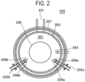
- An exhaust port 231a configured to exhaust an internal atmosphere of the process chamber 201 is installed below the side wall of the reaction tube 203. As shown in FIG. 2 , in the plane view, the exhaust port 231a is provided at a position opposing (facing) the nozzles 249a and 249b (gas supply holes 250a and 250b) with the wafers 200 interposed therebetween.
- the exhaust port 231a may be installed to extend from the lower side to the upper side of the side wall of the reaction tube 203, that is, along the wafer arrangement region.
- An exhaust pipe 231 is connected to the exhaust port 231a.
- a vacuum pump 246 as a vacuum exhauster is connected to the exhaust pipe 231 via a pressure sensor 245 as a pressure detector (pressure detection part) configured to detect an internal pressure of the process chamber 201, and an auto pressure controller (APC) valve 244 as a pressure regulator (pressure regulation part).
- the APC valve 244 is configured to be capable of performing or stopping a vacuum exhaust operation of the interior of the process chamber 201 by being opened or closed while the vacuum pump 246 is actuated, and is also configured to be capable of regulating the internal pressure of the process chamber 201 by adjusting an opening state of the valve based on pressure information detected by the pressure sensor 245 while the vacuum pump 246 is actuated.
- An exhaust system mainly includes the exhaust pipe 231, the APC valve 244, and the pressure sensor 245.
- the exhaust system may include the vacuum pump 246.
- a seal cap 219 which serves as a furnace opening lid configured to be capable of hermetically sealing a lower end opening of the manifold 209, is installed under the manifold 209.
- the seal cap 219 is made of, for example, a metallic material such as SUS, and is formed in a disc shape.
- An O-ring 220b which is a seal making contact with the lower end of the manifold 209, is installed on an upper surface of the seal cap 219.
- a rotator 267 configured to rotate a boat 217 to be described later is installed under the seal cap 219.
- a rotary shaft 255 of the rotator 267 is connected to the boat 217 through the seal cap 219.
- the rotator 267 is configured to rotate the wafers 200 by rotating the boat 217.
- the seal cap 219 is configured to be vertically raised or lowered by a boat elevator 115 as an elevator installed outside the reaction tube 203.
- the boat elevator 115 is constituted as a transporter (transport mechanism) configured to load or unload (transport) the wafers 200 into or out of the process chamber 201 by raising or lowering the seal cap 219.
- a shutter 219s as a furnace opening lid configured to be capable of hermetically sealing the lower end opening of the manifold 209 in a state where the seal cap 219 is lowered and the boat 217 is unloaded from the process chamber 201, is installed under the manifold 209.
- the shutter 219s is made of, for example, a metallic material such as SUS, and is formed in a disc shape.
- An O-ring 220c as a seal making contact with the lower end of the manifold 209 is installed on the upper surface of the shutter 219s.
- the opening/closing operation (elevating operation, rotating operation, or the like) of the shutter 219s are controlled by a shutter opening/closing mechanism 115s.
- a boat 217 as a substrate support is configured to support a plurality of wafers 200, for example, 25 to 200 wafers 200 in such a state that the wafers 200 are arranged in horizontal posture and in multiple stages along a vertical direction with the centers of the wafers 200 aligned with one another. That is, the boat 217 is configured to arrange the wafers 200 to be spaced apart from each other.
- the boat 217 is made of, for example, a heat-resistant material such as quartz or SiC.
- Heat insulating plates 218 made of, for example, a heat-resistant material such as quartz or SiC are supported below the boat 217 in multiple stages.
- a temperature sensor 263 as a temperature detector is installed in the reaction tube 203. Based on temperature information detected by the temperature sensor 263, a state of supplying an electric power to the heater 207 is regulated such that a temperature distribution inside the process chamber 201 becomes a desired temperature distribution.
- the temperature sensor 263 is installed along the inner wall of the reaction tube 203.
- a controller 121 as a control part is constituted as a computer including a central processing unit (CPU) 121a, a random access memory (RAM) 121b, a memory 121c and an I/O port 121d.
- the RAM 121b, the memory 121c, and the I/O port 121d are configured to be capable of exchanging data with the CPU 121a via an internal bus 121e.
- An input/output device 122 including, for example, a touch panel or the like is connected to the controller 121.
- an external memory 123 may be connected to the controller 121.
- the substrate processing apparatus may be configured to include one controller, or may be configured to include a plurality of controllers.
- a control to perform the processing sequence described below may be performed by using one controller, or may be performed by using a plurality of controllers.
- the plurality of controllers may be constituted as a control system connected to one another via a wired or wireless communication network, or the entire control system may perform the control to perform the processing sequence described below.
- controller When the term "controller” is used in the present disclosure, it may include one controller, a plurality of controllers, or a control system constituted by a plurality of controllers.
- the memory 121c includes, for example, a flash memory, a hard disk drive (HDD), a solid state drive (SSD), or the like.
- a control program that controls the operation of the substrate processing apparatus, a process recipe in which sequences and conditions of substrate processing process to be described below are written, and the like are readably stored in the memory 121c.
- the process recipe functions as a program configured to cause, by the controller 121, the substrate processing apparatus to perform the respective sequences in a below-described substrate processing process, to obtain a predetermined result.
- the process recipe, the control program, and the like are generally and simply referred to as a "program.” Furthermore, the process recipe may be simply referred to as a "recipe.” When the term “program” is used herein, it may indicate a case of including the recipe, a case of including the control program, or a case of including both the recipe and the control program.
- the RAM 121b is constituted as a memory area (work area) in which programs, data and the like read by the CPU 121a are temporarily held.
- the I/O port 121d is connected to the MFCs 241a to 241e, the valves 243a to 243e, the pressure sensor 245, the APC valve 244, the vacuum pump 246, the temperature sensor 263, the heater 207, the rotator 267, the boat elevator 115, the shutter opening/closing mechanism 115s, and the like.
- the CPU 121a is configured to be capable of reading and executing the control program from the memory 121c and reading the recipe from the memory 121c in response to an input of an operation command from the input/output device 122 or the like.
- the CPU 121a is configured to be capable of controlling flow rate regulation operations of various materials (various gases) by the MFCs 241a to 241e, opening/closing operations of the valves 243a to 243e, an opening/closing operation of the APC valve 244, an pressure regulation operation performed by the APC valve 244 based on the pressure sensor 245, an operation of actuating or stopping the vacuum pump 246, a temperature regulation operation performed by the heater 207 based on the temperature sensor 263, operations of rotating the boat 217 and adjusting a rotation speed of the boat 217 with the rotator 267 , an operation of raising or lowering the boat 217 by the boat elevator 115, an opening/closing operation of the shutter 219s by the shutter opening/closing mechanism 115s, and the like
- the controller 121 may be constituted by installing, in the computer, the above-described program recorded and stored in an external memory 123.
- the external memory 123 includes, for example, a magnetic disk such as a HDD, an optical disc such as a CD, a magneto-optical disc such as a MO, a semiconductor memory such as a USB memory or a SSD, and so forth.
- the memory 121c and the external memory 123 are constituted as a computer-readable recording medium.
- the memory 121c and the external memory 123 are generally and simply referred to as a recording medium.
- the term "recording medium” may indicate a case of including the memory 121c, a case of including the external memory 123, or a case of including both the memory 121c and the external memory 123.
- the program may be installed to the computer by using a communication means or unit such as the Internet or a dedicated line instead of using the external memory 123.
- a method of processing a substrate i.e., an example of a processing sequence of forming an oxide film over a wafer 200 as the substrate, will be described mainly with reference to FIGS. 4 to 7 .
- a wafer 200 including a recess structure 300 such as a trench, a groove, or a hole, which is a three-dimensional structure
- operations of the respective components constituting the substrate processing apparatus are controlled by the controller 121.
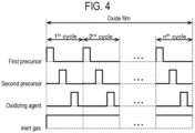
- a processing sequence includes forming an oxide film containing a predetermined element over the wafer 200 by performing a cycle a predetermined number of times (n times, where n is an integer of 1 or 2 or more), the cycle including:
- the predetermined element contained in the first precursor and the second precursor is a main element that constitutes the second layer and the oxide film formed over the wafer 200.
- a Si film is formed as a base over the surface of the wafer 200 will be described.
- wafer used herein may refer to a wafer itself or a stacked body of a wafer and a predetermined layer or film formed over a surface of the wafer.
- a surface of a wafer used herein may refer to a surface of a wafer itself or a surface of a predetermined layer or the like formed over a wafer.
- the expression “a predetermined layer is formed over a wafer” used herein may mean that a predetermined layer is directly formed over a surface of a wafer itself or that a predetermined layer is formed over a layer or the like formed over a wafer.
- substrate used herein may be synonymous with the term "wafer.”
- the term "agent” includes at least one selected from the group of a gaseous substance and a liquid substance.
- the liquid substance includes a mist-like substance. That is, each of the first precursor, the second precursor, and the oxidizing agent may include a gaseous substance, a liquid substance such as a mist-like substance or the like, or both.
- the term "layer” includes at least one selected from the group of a continuous layer and a discontinuous layer.
- the first layer and the second layer may include continuous layers, discontinuous layers, or both.
- the description that the first precursor, the second precursor, and the oxidizing agent are adsorbed to or react with the surface of the wafer 200 includes a case where the first precursor, the second precursor, and the oxidizing agent are adsorbed to or react with the surface of the wafer while remaining undecomposed, and a case where intermediates produced by decomposition of the first precursor, the second precursor, and the oxidizing agent or desorption of ligands of the first precursor, the second precursor, and the oxidizing agent are adsorbed to or react with the surface of the wafer 200.
- the shutter 219s is moved by the shutter opening/closing mechanism 115s to open the lower end opening of the manifold 209 (shutter opening).
- the boat 217 supporting the plurality of wafers 200 is lifted by the boat elevator 115 to be loaded into the process chamber 201 (boat loading).
- the seal cap 219 seals the lower end of the manifold 209 via the O-ring 220b. In this way, the wafers 200 are prepared (provided) inside the process chamber 201.
- the inside of the process chamber 201 is vacuum-exhausted (depression-exhausted) by the vacuum pump 246 to reach a desired pressure (state of vacuum).
- the internal pressure of the process chamber 201 is measured by the pressure sensor 245, and the APC valve 244 is feedback-controlled based on the measured pressure information.
- the wafers 200 in the process chamber 201 are heated by the heater 207 to reach a desired processing temperature.
- a state of supplying electric power to the heater 207 is feedback-controlled based on the temperature information detected by the temperature sensor 263 such that a temperature distribution inside the process chamber 201 becomes a desired temperature distribution.
- the rotation of the wafers 200 by the rotator 267 is started.
- the exhaust of the inside of the process chamber 201 and the heating and rotation of the wafers 200 are continuously performed at least until the processing on the wafers 200 is completed.
- a first precursor containing a predetermined element and a halogen element is supplied to the wafers 200 in the process chamber 201.
- valve 243a is opened to allow the first precursor to flow through the gas supply pipe 232a.
- a flow rate of the first precursor is regulated by the MFC 241a.
- the first precursor is supplied into the process chamber 201 via the nozzle 249a, and is exhausted via the exhaust port 231a. At this time, the first precursor is supplied to the wafers 200 (supply of first precursor).
- the valves 243d and 243e may be opened to supply an inert gas into the process chamber 201 via the nozzles 249a and 249b.
- a processing condition when supplying the first precursor in this step is exemplified as follows.
- the processing pressure in this step may be lower than the processing pressure in step B. Further, a partial pressure of the first precursor supplied to the wafers 200 in this step may be lower than a partial pressure of the second precursor supplied to the wafers 200 in step B. From the viewpoint of improving a processing speed, the processing temperature may be substantially the same in steps A to C.
- the first precursor when a precursor containing a bond between the predetermined elements (where two elements are both the predetermined element) is used as the first precursor, in this step, the first precursor may be supplied to the wafers 200 under a processing condition in which the bond of the predetermined elements contained in the first precursor is broken in a gas phase.
- the processing condition mentioned above includes at least one selected from the group of a processing temperature, a processing pressure, presence or absence of plasma excitation, and a magnitude of energy given during plasma excitation.
- a processing temperature in the present disclosure means a temperature of the wafers 200 or an internal temperature of the process chamber 201
- a processing pressure means an internal pressure of the process chamber 201, that is, a pressure of the space where the wafers 200 are placed.
- a processing time means a time during which the processing is continued.
- the supply flow rate includes 0 slm
- 0 slm means that the substance (gas) is not supplied. The same applies to the following description.
- the first precursor containing the predetermined element and the halogen element By supplying the first precursor containing the predetermined element and the halogen element to the wafers 200 under the above-described processing condition, the first precursor is adsorbed to the surface of the wafer 200, it is possible to form a first layer containing the predetermined element and including a surface terminated with the halogen element (see FIG. 5A ).
- the bond between the predetermined element and the halogen element in the first precursor may be partially broken, and the predetermined element containing dangling bonds may be adsorbed to the adsorption sites on the surface of the wafer 200 to form the first layer.
- the bond between the predetermined elements contained in the first precursor may be broken, and the predetermined element containing dangling bonds may be adsorbed to the adsorption sites on the surface of the wafer 200 to form the first layer.
- terminations such as OH terminations are present as the adsorption sites on the surface of the wafer 200.
- the adsorption sites on the surface of the wafer 200 are at least partially occupied by the halogen-terminated first layer.
- an oxidizing agent is supplied to the wafer 200, such that terminations such as OH terminations, which becomes adsorption sites in steps A and B, are formed over the outermost surface of the wafer 200.
- a first layer containing a predetermined element and containing terminations of a halogen element (halogen terminations) formed over a surface of the first layer may be discontinuously formed over an upper surface and at least a portion of an inner surface of the recess structure 300 (specifically, side and bottom surfaces inside the recess structure 300).
- the first precursor (predetermined element) may be adsorbed preferentially to an opening side 301 of the recess structure 300 to form the first layer (see FIG. 5A ).
- the first layer may be formed such that a density of the first layer formed at an upper end of a side surface of the opening side 301 of the recess structure 300 (a side surface of an opening of the recess structure 300) is greater than a density of the first layer formed at a lower end of a deep side 302 of the recess structure 300 (a side surface of a lower end of the recess 300 and/or a bottom surface of the recess structure 300).
- density of a layer at the upper surface and the inner surface of the recess structure 300 may be synonymous with, for example, the number of adsorbed predetermined elements bonded with halogen elements (i.e., terminated with halogen elements) per unit area at the inner surface of the recess structure 300, or an average thickness of a layer per unit area at the inner surface of the recess structure 300.
- the first layer may be formed discontinuously over the entire inner surface of the recess structure 300.
- the processing temperature is less than 350 degrees C, it may be difficult to enable chemical adsorption to the inner surface of the recess structure 300, and it may be difficult to form the first layer at a practical rate.
- the processing temperature is set to 350 degrees C or higher, it becomes possible to form the first layer over the inner surface of the recess structure 300 at a practical rate.
- the bond between the predetermined elements contained in the first precursor may not be broken in the gas phase, such that it may be difficult for the predetermined element to be adsorbed to the inner surface of the recess structure 300.
- processing temperature 500 degrees C or higher, it is possible to break the bond between the predetermined elements contained in the first precursor and promote adsorption of the predetermined element to the inner surface of the recess structure 300.
- the first precursor may be thermally decomposed excessively in the gas phase, and the predetermined element tends to be locally deposited near the upper end of the inner surface of the recess structure 300, which make it difficult to form a first layer with a desired layer thickness distribution on a side wall or a bottom surface of the inner surface of the recess structure 300.
- the processing temperature By setting the processing temperature to 700 degrees C or lower, it becomes possible to form a first layer with a desired layer thickness distribution on the side wall or the bottom surface of the inner surface of the recess structure 300.
- step C By setting the processing temperature to 600 degrees C or less, it becomes easier to form a first layer with a desired layer thickness distribution on the side wall or the bottom surface of the inner surface of the recess structure 300.
- step C when the same processing temperature is maintained in step C, which will be described later, by setting the processing temperature to 600 degrees C or less, it is possible to suppress excessive thermal decomposition of the oxidizing agent supplied in step C, and it is possible to achieve a practical deposition rate.
- the halogen terminations formed over the surface of the first layer suppresses (inhibits) adsorption of at least one selected from the group of a second precursor supplied in below-described step B or predetermined element contained in the second precursor.
- the first layer constitutes an adsorption inhibition layer that inhibits adsorption of at least one selected from the group of the second precursor and the predetermined element contained in the second precursor to the first layer.
- a gas containing a predetermined element and a halogen element may be used.
- the predetermined element is Si
- a halosilane gas may be used as the first precursor.
- the halogen element at least one selected from the group of chlorine (Cl), fluorine (F), bromine (Br), and iodine (I) may be used.
- a chlorosilane-based gas such as a tetrachlorosilane (SiCl 4 ) gas, a monochlorosilane (SiH 3 Cl) gas, a dichlorosilane (SiH 2 Cl 2 ) gas, or a trichlorosilane (SiHCl 3 ) gas, which does not contain any Si-Si bond (i.e., any bond between predetermined elements) in one molecule.
- a chlorosilane-based gas such as a tetrachlorosilane (SiCl 4 ) gas, a monochlorosilane (SiH 3 Cl) gas, a dichlorosilane (SiH 2 Cl 2 ) gas, or a trichlorosilane (SiHCl 3 ) gas, which does not contain any Si-Si bond (i.e., any bond between predetermined elements) in one molecule.
- a fluorosilane-based gas such as a tetrafluorosilane (SiF 4 ) gas, a difluorosilane (SiH 2 F 2 ) gas or the like, a bromosilane-based gas such as a tetrabromosilane (SiBr 4 ) gas, a dibromosilane (SiH 2 Br 2 ) gas or the like, and an iodosilane-based gas such as a tetraiodosilane (SiI 4 ) gas, a diiodosilane (SiH 2 I 2 ) gas or the like, which do not contain any Si-Si bond (i.e., any bond between predetermined elements) in one molecule.
- a gas that does not contain hydrogen (H) in one molecule such as a gas that does not contain hydrogen (H) in one molecule, such
- a chlorosilane-based gas such as a hexachlorodisilane (Si 2 Cl 6 ) gas, an octachlorotrisilane (Si 3 Cl 8 ) gas, a monochlorodisilane (Si 2 H 5 Cl) gas, a dichlorodisilane (Si 2 H 4 Cl 2 ) gas, a trichlorodisilane (Si 2 H 3 Cl 3 ) gas, a tetrachlorodisilane (Si 2 H 2 Cl 4 ) gas, a monochlorotrisilane (SisHsCl) gas, a dichlorotrisilane (Si 3 H 4 Cl 2 ) gas or the like, which contains a Si-Si bond (i.e., a bond between predetermined elements) in one molecule.
- a chlorosilane-based gas such as a hexachlorodisilane (Si 2 Cl 6 ) gas, an
- the first precursor it may be possible to use other halosilane-based gases with molecular structures in which Cl atoms in molecular structures of these chlorosilane-based gases are replaced with atoms of other halogen elements.
- these gases as the first precursor, it is possible to use a gas that does not contain H, such as the Si 2 Cl 6 gas or the Si 3 Cl 8 gas.
- One or more of these gases may be used as the first precursor.
- the inert gas it may be possible to use a nitrogen (N 2 ) gas, or a rare gas such as an argon (Ar) gas, a helium (He) gas, a neon (Ne) gas, a xenon (Xe) gas or the like.
- a nitrogen (N 2 ) gas or a rare gas such as an argon (Ar) gas, a helium (He) gas, a neon (Ne) gas, a xenon (Xe) gas or the like.
- Ar argon
- He helium
- Ne neon
- Xe xenon
- the valve 243a is closed to stop the supply of the first precursor into the process chamber 201. Then, the inside of the process chamber 201 is vacuum-exhausted to remove gaseous substances remaining inside the process chamber 201 from the inside of the process chamber 201. At this time, the valves 243d and 243e are opened to supply an inert gas into the process chamber 201 via the nozzles 249a and 249b. The inert gas supplied from the nozzles 249a and 249b acts as a purge gas, thereby purging the space where the wafers 200 exist, i.e., the inside of the process chamber 201.
- a second precursor containing a predetermined element and an amino group bonded to the predetermined element in one molecule is supplied to the wafer 200 in the process chamber 201, i.e., the wafer 200 in which the first layer is formed over the inner surface of the recess structure 300.
- a second precursor containing a predetermined element and a single amino group bonded to the predetermined element in one molecule is supplied. That is, the single amino group is a sole amino group which is bonded to the predetermined element in one molecule of the second precursor.
- valve 243c is opened to allow the second precursor to flow through the gas supply pipe 232c.
- a flow rate of the second precursor is regulated by the MFC 241c.
- the second precursor is supplied into the process chamber 201 via the nozzle 249a, and is exhausted via the exhaust port 231a.
- the second precursor is supplied to the wafer 200 (supply of second precursor).
- the valves 243d and 243e may be opened to supply an inert gas into the process chamber 201 via the nozzles 249a and 249b respectively.
- a processing condition when the second precursor is supplied in this step may be exemplified as follows.
- processing conditions may be the same as those used when the first precursor is supplied in step A. However, this step is performed under a processing condition in which the predetermined element contained in the second precursor may be adsorbed to the wafer 200 by supplying the second precursor to the wafer 200 over which the first layer is not formed.
- the processing condition referred to herein include at least one selected from the group of a temperature condition and a pressure condition. Further, the processing pressure in this step may be higher than the processing pressure in step A. Moreover, a partial pressure of the second precursor supplied to the wafer 200 in this step is higher than a partial pressure of the first precursor supplied to the wafer 200 in step A.
- the second precursor may be mainly adsorbed to locations at the first layer over the surface of the wafer 200 where halogen terminations are not formed (i.e., adsorption sites remaining on the surface of the wafer 200, which are not terminated with halogen elements), thereby forming a second layer containing the predetermined element (see FIG. 5B ).
- the predetermined element which contains dangling bonds due to desorption of the amino groups from molecules of the second precursor, is adsorbed to the adsorption sites on the surface of the wafer 200 over which the first layer is not formed, whereby the second layer may be formed over the wafer 200.
- the halogen elements terminating the first layer react with the amino groups contained in the second precursor, such that at least a portion of the halogen elements is desorbed from the surface of the wafer 200 (the surface of the first layer).
- a deposition rate of the second layer over the surface of the deep side 302 may be lower than a deposition rate of the second layer over the surface of the opening side 301 due to an imbalance in a supply amount of the second precursor, which may deteriorate a step coverage of the second layer. Further, as the step coverage of the second layer is deteriorated, a step coverage of the oxide film formed by modifying (oxidizing) the second layer may also be deteriorated.
- the first layer that inhibits the adsorption of the second precursor is formed such that a density of the first layer becomes larger at an upper end of the opening side 301 than at a lower end of the deep side 302 (the bottom surface of the opening of the recess structure 300). Therefore, the adsorption of the second precursor is further suppressed at the opening side 301 than at the deep side 302. As a result, an action of the first layer reducing a density of the second layer is greater at the opening side 301 than at the deep side 302.
- the deposition rate of the second layer at the deep side 302 may be greater than the deposition rate of the second layer at the opening side 301, as compared with the case where the first layer is not formed.
- a thickness distribution of the second layer may be controlled to increase the deposition rate of the second layer at the deep side 302 and reduce the deposition rate of the second layer at the opening side 301, as compared to the case where the first layer is not formed.
- the thickness distribution of the second layer may be controlled such that the deposition rate of the second layer at the deep side 302 is higher than the deposition rate of the second layer at the opening side 301, or the deposition rate of the second layer at the deep side 302 and deposition rate of the second layer at the opening side 301 are substantially equal to each other.
- the processing temperature is 500 degrees C or lower, it may be difficult for the predetermined element contained in the second precursor to be adsorbed to the inner surface of the recess structure 300, making it difficult to form the second layer at a practical rate.
- the processing temperature by setting the processing temperature to a temperature exceeding 500 degrees C, it becomes possible to form the second layer over the inner surface of the recess structure 300 at a practical rate.
- the processing pressure is less than 100 Pa
- the adsorption of the second precursor to the inner surface of the recess structure 300 becomes difficult to occur, which may make it difficult to form the second layer at a practical rate.
- the processing pressure is set to 100 Pa or more, it is possible to promote the adsorption of the second precursor to the inner surface of the recess structure 300, thereby forming the second layer at a practical rate.
- this step for example, by setting the processing temperature to a temperature exceeding 500 degrees C, and setting the processing pressure to 100 Pa or more, it is possible to achieve the processing conditions under which, the predetermined element contained in the second precursor may be adsorbed, at a practical rate, even to the surface of the wafer 200 over which the first layer is not formed.
- the processing temperature exceeds 700 degrees C
- the second precursor is thermally decomposed excessively in the gas phase, and the predetermined element tends to be locally deposited in multiple layers near the upper end of the inner surface of the recess structure 300, which may make it difficult to form the second layer with an excellent step coverage.
- the processing temperature By setting the processing temperature to 700 degrees C or lower, it is possible to form the second layer with an excellent step coverage.
- the second precursor it may be possible to use a gas containing a predetermined element and an amino group bonded to the predetermined element in one molecule. That is, when the predetermined element is Si, an aminosilane-based gas may be used as the second precursor.
- the second precursor it is possible to use a gas containing a predetermined element and a single amino group bonded to the predetermined element in one molecule.
- the predetermined element is Si
- an aminosilane-based gas containing Si and an amino group, in which a single amino group is bonded to one Si contained in one molecule.
- the amino group refers to a functional group in which one or two hydrocarbon groups containing one or more carbon (C) atoms are coordinated to one nitrogen (N) atom (a functional group in which one H or both H's of the amino group represented by NH 2 is substituted with a hydrocarbon group containing one or more C atoms).
- N nitrogen
- the two hydrocarbon groups may be the same hydrocarbon group or different hydrocarbon groups.
- the hydrocarbon groups may contain a single bond like an alkyl group, or may contain an unsaturated bond such as a double bond or triple bond.
- the amino group may contain a cyclic structure.
- the amino group in aminosilane may also be referred to as a ligand or an amino ligand.
- the aminosilane-based gas may also contain a hydrocarbon group in addition to Si and an amino group.
- the hydrocarbon groups may contain a single bond like an alkyl group, or may contain an unsaturated bond such as a double bond or triple bond.
- the hydrocarbon groups may contain a cyclic structure.
- the hydrocarbon groups may be bonded to Si, which is a central atom of an aminosilane molecule, and in such a case, the hydrocarbon group in aminosilane may also be referred to as a ligand or a hydrocarbon ligand.
- the hydrocarbon group is an alkyl group
- the hydrocarbon group may also be referred to as an alkyl ligand.
- an aminosilane-based gas including a (dialkylamino)trialkylsilane gas such as a (dimethylamino)trimethylsilane ((CH 3 ) 2 NSi(CH 3 ) 3 ) gas, a diethylaminotrimethylsilane ((C 2 H 5 ) 2 NSi(CH 3 ) 3 ) gas, a diethylaminotriethylsilane ((C 2 H 5 ) 2 NSi(C 2 H 5 ) 3 ) gas, a dimethylaminotriethylsilane ((CH 3 ) 2 NSi(C 2 H 5 ) 3 ) gas or the like, a mono(dialkylamino)silane gas such as a (diisobutylamino)silane ((C 4 H 9 ) 2 NSiH 3 ) gas, a (diisopropylamino)silane ((C)
- One or more of these gases may be used as the second precursor.
- a gas in which a bonding hand other than bonding hands of Si bonded to the single amino group is bonded to H such as the ((C 4 H 9 ) 2 NSiH 3 ) gas, the ((C 3 H 7 ) 2 NSiH 3 ) gas, the (SiH 3 (N(CH 3 )(C 2 H 5 ))) gas, the (SiH 3 (N(CH 3 ) 2 )) gas or the like.
- an aminosilane-based gas including a bis(dialkylamino)dialkylsilane gas such as a bis(dimethylamino)dimethylsilane ([(CH 3 ) 2 N] 2 Si(CH 3 ) 2 ) gas or the like, a tris(dialkylamino)alkylsilane gas such as a tris(dimethylamino)methylsilane ([(CH 3 ) 2 N] 3 SiCH 3 ) gas or the like, a bis(dialkylamino)silane gas such as a bis(diethylamino)silane ([(C 2 H 5 ) 2 N] 2 SiH 2 ) or the like, a bis(monoalkylamino)silane gas such as a bis(tert-butylamino)silane ([(C 4 H 9 )NH] 2 SiH 2 ) gas or the like, a tris(
- the valve 243c is closed to stop the supply of the precursor into the process chamber 201. Then, the inside of the process chamber 201 is vacuum-exhausted to remove gaseous substances remaining inside the process chamber 201 from the inside of the process chamber 201. At this time, the valves 243d and 243e are opened to supply an inert gas into the process chamber 201 via the nozzles 249a and 249b. The inert gas supplied from the nozzles 249a and 249b acts as a purge gas, thereby purging a space where the wafers 200 exist, i.e., the inside of the process chamber 201.
- step B an oxidizing agent that oxidizes the second layer is supplied to the wafers 200 in the process chamber 201, i.e., the wafers 200 in which the second layer is formed over the inner surface of the recess structure 300.
- valve 243b is opened to allow the oxidizing agent to flow through the gas supply pipe 232b.
- a flow rate of the oxidizing agent is regulated by the MFC 241b.
- the oxidizing agent is supplied into the process chamber 201 via the nozzle 249b, and is exhausted via the exhaust port 231a. At this time, the oxidizing agent is supplied to the wafers 200 (supply of oxidizing agent).
- the valves 243d and 243e may be opened to supply an inert gas into the process chamber 201 via the nozzles 249a and 249b.
- a processing condition when the oxidizing agent is supplied in this step is exemplified as follows:
- Non-plasma gas that is not plasma-excited (non-plasma state).
- the oxidizing agent By supplying the oxidizing agent to the wafers 200 under the above-described processing conditions at least a portion of the second layer formed over the inner surface of the recess structure 300 is oxidized by reacting with the oxidizing agent. As a result, a third layer, which is an oxide layer of the second layer, is formed over the inner surface of the recess structure 300.
- the third layer is a layer containing a predetermined element.
- impurities such as a halogen element and the like contained in the second layer is desorbed from the second layer as gaseous substances during the oxidizing reaction process for the third layer, and is discharged from the inside of the process chamber 201.
- the third layer becomes a layer containing fewer impurities such as a halogen element and the like than the second layer formed in step B.
- the oxidizing agent it may be possible to use an oxygen (O)-containing gas (O-containing substance).
- O-containing gas it may be possible to use an oxygen (O 2 ) gas, an ozone (O 3 ) gas, a nitrous oxide (N 2 O) gas, a nitric oxide (NO) gas, a nitrogen dioxide (NO 2 ) gas, a carbon monoxide (CO) gas, a carbon dioxide (CO 2 ) gas or the like.
- One or more of these gases may be used as the oxidizing agent.
- the oxidizing agent it may be possible to use an O- and H-containing gas (an O- and H-containing substance).
- the O- and H-containing gas it may be possible to use a water vapor (H 2 O) gas, a hydrogen peroxide (H 2 O 2 ) gas, H 2 gas+O 2 gas, H 2 gas+O 3 gas, or the like. That is, as the O- and H-containing gas, O-containing gas+H-containing gas may also be used. In this case, as the H-containing gas, a deuterium ( 2 H 2 ) gas may be used instead of the H 2 gas. As the oxidizing agent, one or more of these gases may be used.
- a silicon oxide layer (SiO layer) is formed as the third layer over the surface of the wafer 200.
- description of two gases together such as "H 2 gas+O 2 gas” means a mixed gas of a H 2 gas and an O 2 gas.
- two gases may be mixed (premixed) in a supply pipe and then supplied into the process chamber 201, or two gases may be separately supplied to the process chamber 201 via different supply pipes and then mixed (post-mixed) within the process chamber 201.
- the oxidizing agent the O-containing gas that does not contain H, such as an O 2 gas or an O 3 gas.
- the oxidizing agent when a processing temperature exceeds a specific temperature (e.g., 600 degrees C), the oxidizing agent may be thermally decomposed excessively and the oxidizing power thereof may decrease, thereby making it difficult to oxidize the second layer.
- a specific temperature e.g. 600 degrees C
- the processing temperature By setting the processing temperature to a specific temperature (e.g., 600 degrees C) or lower, it is possible to oxidize the second layer even when such an oxidizing agent is used.
- the valve 243b is closed to stop the supply of the oxidizing agent into the process chamber 201. Then, the inside of the process chamber 201 is vacuum-exhausted to remove gaseous substances remaining inside the process chamber 201 from the inside of the process chamber 201. At this time, the valves 243d and 243e are opened to supply an inert gas into the process chamber 201 via the nozzles 249a and 249b. The inert gas supplied via the nozzles 249a and 249b acts as a purge gas, thereby purging the space where the wafers 200 exist, i.e., the inside of the process chamber 201.
- n times (where n is an integer of 1 or 2 or more), an oxide film with a desired composition is formed over the surface of the wafer 200 (the inner surface of the recess structure 300) (see FIG. 5C ). Further, by setting the number of cycles n to the number of times by which the inside of the recess structure 300 is filled with an oxide film, the inside of the recess structure 300 is filled with the oxide film. For example, when a gas containing the above-described Si and amino group as the second precursor, a silicon oxide film (SiO film) is formed over the surface of the wafer 200.
- SiO film silicon oxide film
- the above-described cycle is performed multiple times.
- a thickness of the third layer formed per cycle is set to be smaller than a desired thickness, and the above-mentioned cycle is performed multiple times until a thickness of the oxide film formed by stacking the third layer reaches the desired thickness.
- the cycle performed at an m-th time may be different from the cycle performed at an (m+1)-th time in at least one selected from the group of the supply time, the partial pressure, and the processing pressure of the first precursor in step A, which is executed in the cycle performed at the (m+1)-th time.
- at least one selected from the group of the supply time, the partial pressure, and the processing pressure of the first precursor in step A executed in the cycle performed at the (m+1)-th time may be different from those of the first precursor in step A executed up to the cycle performed at the m-th time.
- the supply time of the first precursor in step A executed in the cycle performed at the (m+1)-th time may be set to be longer than the supply time of the first precursor in step A executed in the cycle performed at the m-th time
- the partial pressure of the first precursor in step A executed in cycle performed at the (m+1)-th time may be set to be higher than the partial pressure of the first precursor in step A executed in the cycle performed at the m-th time
- the processing pressure in step A executed in the cycle performed at the (m+1)-th time may be set to be higher than the processing pressure in step A executed in the cycle performed at the m-th time.
- a density of the first layer formed on the upper end of the opening side 301 may be increased. Therefore, it is possible to strengthen a film formation inhibition effect of the first layer, and it is possible to form the second layer from the lower end of the deep side 302 (the bottom surface of the opening) toward the side surface of the opening. As a result, the step coverage may be maintained even when the aspect ratio is increased.
- the supply time of the first precursor in step A executed in the cycle performed at the (m+1)-th time may be set to be shorter than the supply time of the first precursor in step A executed in the cycle performed at the m-th time
- the partial pressure of the first precursor in step A executed in the cycle performed at the (m+1)-th time may be set to be lower than the partial pressure of the first precursor in step A executed in the cycle performed at the m-th time
- the processing pressure in step A executed in the cycle performed at the (m+1)-th time may be set to be lower than the processing pressure in step A executed in the cycle performed at the m-th time.
- an inert gas as a purge gas is supplied into the process chamber 201 via each of the nozzles 249a and 249b, and is exhausted via the exhaust port 231a.
- the inside of the process chamber 201 is purged, and gases, reaction byproducts, and the like remaining in the process chamber 201 are removed from the inside of the process chamber 201 (after-purge).
- the atmosphere inside the process chamber 201 is replaced with the inert gas (inert gas replacement), and the pressure inside the process chamber 201 is returned to the atmospheric pressure (returning to atmospheric pressure).
- the seal cap 219 is lowered by the boat elevator 115, and the lower end of the manifold 209 is opened.
- the processed wafers 200 are then unloaded from the lower end of the manifold 209 to the outside of the reaction tube 203 while being supported by the boat 217 (boat unloading).
- the shutter 219s is moved and the lower end opening of the manifold 209 is sealed by the shutter 219s via the O-ring 220c (shutter closing).
- the processed wafers 200 are discharged from the boat 217 after being unloaded to the outside of the reaction tube 203 (wafer discharging).
- step B by using the second precursor containing a single amino group, which is relatively easy to react with the halogen element terminating the first layer, in one molecule, it is possible to minimize the desorption of the halogen element terminating the first layer. This makes it possible to enhance an inhibitor effect of inhibiting the adsorption of the predetermined element to the first layer, as compared with a case of using a precursor containing a plurality of amino groups in one molecule. As a result, it is possible to improve the step coverage of the oxide film formed over the inner surface of the recess structure of the wafer 200.
- the second precursor contains a single amino group in one molecule
- the predetermined element contained in the second precursor is adsorbed to the surface of the wafer 200 in step B, it is possible to reduce an amount of residual amino groups remaining in the second layer without being desorbed. This makes it difficult for impurities (C or N) derived from amino groups to remain in the oxide film.
- step A by forming the first layer by using a precursor containing a predetermined element as the first precursor, it is possible to increase the adsorption rate of the precursor (the deposition rate of the first layer), as compared with a case of forming the first layer by using a compound composed of a halogen element,. Thus, it is possible to shorten the time to form the first layer.
- the predetermined element contained in the first layer which acts as an adsorption-inhibiting layer (inhibitor layer) for the second precursor, may also make contribution as a portion of the oxide film, which makes it possible to improve the deposition rate of the oxide film.
- step B is executed under the processing condition in which the predetermined element contained in the second precursor may be adsorbed to the wafer 200 by supplying the second precursor to the wafer 200 over which the first layer is not formed.
- step B is performed under the processing condition that allow the predetermined element contained in the second precursor to be adsorbed to the wafer 200 without executing step A, for example, the processing condition at higher temperature and pressure than the condition under which the predetermined element contained in the second precursor may not be adsorbed to the surface of the wafer 200 over which the first layer is not formed.
- the predetermined element may be adsorbed to the adsorption sites on the surface of the wafer 200 in a state in which the first layer inhibits the adsorption of the predetermined element contained in the second precursor.
- step B By setting the partial pressure of the second precursor supplied to the wafer 200 in step B to be higher than the partial pressure of the first precursor supplied to the wafer 200 in step A, i.e., by supplying the second precursor containing a predetermined element and an amino group at a relatively high partial pressure, the second precursor may be easily activated and the amino group may be easily desorbed from the second precursor. This makes it possible to promote adsorption of the predetermined element containing dangling bonds to the wafer 200, thereby increasing the deposition rate. The same applies to a case where the processing pressure in step B is set to be higher than the processing pressure in step A.
- the partial pressure of the first precursor supplied to the wafer 200 in step A is lower than the partial pressure of the second precursor supplied to the wafer 200 in step B, i.e., by supplying the first precursor at a relatively low partial pressure, it is possible to suppress excessive thermal decomposition of the first precursor, and it is possible to avoid a decrease in the step coverage due to local multiple deposition of the predetermined element near the upper end of the recess structure 300 on the wafer 200.
- the processing pressure in step A is lower than the processing pressure in step B.
- the bond between the predetermined elements may be broken by thermal decomposition or the like, and a highly reactive intermediate containing a halogen element and dangling bonds of the predetermined element may be produced with ease.
- This may promote the formation of a first layer terminated with the halogen element over the surface of the wafer 200.
- the formation of the first layer may be easily promoted by producing such an intermediate. This is because when step C is executed and OH terminations are formed at the surface of the oxide film, these OH terminations function as adsorption sites.
- step A may be performed under a higher temperature condition or a higher pressure condition to generate the above-described highly reactive intermediate when using a gas not containing the bond between the predetermined elements in one molecule as the first precursor. Further, even when using a gas containing the halogen element but not containing the predetermined element as a modifying agent, a higher temperature condition or a higher pressure condition may be demanded for bringing the gas into a state of being highly reactive as described above.
- step A by supplying the first precursor under the processing condition in which the bond between the predetermined elements is broken in the gas phase, the highly reactive intermediate containing the halogen element and containing the dangling bond of the predetermined element may be generated in the gas phase. This may promote the formation of the first layer over the surface of the wafer 200 for the same reasons as described above.
- the predetermined element contained in the second precursor may be adsorbed well to the adsorption site on the surface of the wafer 200, which makes it possible to increase the density of the predetermined element in the second layer. Further, by increasing the density of the predetermined element in the second layer, it is possible to increase the deposition rate of the oxide film. Moreover, when the second precursor is adsorbed to the surface of the wafer 200, elements (C, etc.) other than H contained in the second precursor may be prevented from remaining in the oxide film while being bonded to the predetermined element. That is, it is possible to reduce impurities derived from the ligand in the oxide film.
- step C By using an O-containing gas that does not contain H as the oxidizing agent, i.e., by not supplying the H-containing gas in step C, the halogen element constituting the halogen terminations remaining on the surface of the first layer may be prevented from being desorbed by reacting with H.
- step B of the next cycle it is possible to improve the adsorption inhibition effect of suppressing adsorption of the predetermined element contained in the second precursor to the surface of the first layer.
- an O-containing gas containing H as the oxidizing agent.
- step C By performing step C by using a gas that is not excited by plasma (i.e., non-plasma gas), it is possible to suppress desorption of the halogen element constituting the halogen terminations remaining on the surface of the first layer.
- the non-plasma gas includes, for example, a thermally-excited gas. Therefore, in step B of the next cycle, it is possible to improve the adsorption inhibition effect of suppressing adsorption of the predetermined element contained in the second precursor to the surface of the first layer.
- step C when step C is performed by using a plasma-excited gas, the halogen element constituting the halogen terminations remaining on the surface of the first layer is rapidly desorbed. Therefore, it may be difficult to regulate a desorption amount of the halogen element.
- step C by performing step C by using a non-plasma gas, the desorption amount of the halogen element constituting the halogen terminations remaining on the surface of the first layer may be regulated, and an adsorption amount of the predetermined element contained in the second precursor to the surface of the first layer may be controlled in step B of the next cycle.
- the oxidizing agent in a plasma-excited state.
- step A the first layer is formed such that the density of the first layer formed on the opening side 301 of the recess structure 300 is larger than the density of the first layer formed on the deep side 302.
- the deposition rate of the oxide film over the surface of the deep side 302 may be made greater than the deposition rate of the oxide film over the surface of the opening side 301. That is, by forming the first layer in this manner, as compared with a case where the first layer is not formed, a thickness distribution of the oxide film may be controlled to increase the deposition rate of the oxide film over the surface of the deep side 302 and reduce the deposition rate of the oxide film over the surface of the opening side 301.
- the thickness distribution of the second layer may be controlled such that the deposition rate of the oxide film over the surface of the deep side 302 is greater than the deposition rate of the oxide film over the surface of the opening side 301, or the deposition rate of the oxide film over the surface of the deep side 302 and the deposition rate of the oxide film over the surface of the opening side 301 are substantially equal to each other. As a result, it is possible to improve the step coverage of the oxide film formed over the inner surface of the recess structure 300.
- processing sequence according to the embodiments of the present disclosure may be modified as shown in the following modifications. These modifications may be combined arbitrarily. Unless otherwise specified, a processing procedure and a processing condition in each step of each modification may be the same as the processing procedure and processing condition in each step of the processing sequence described above.
- steps A, B, and C may be performed in this order while an execution period of step A and an execution period of step B overlap each other at least partially.
- a cycle time may be shortened and a productivity of the film-forming process may be improved.
- a first cycle including steps A, B, and C may be performed a first number of times (n1 times where n1 is an integer of 1 or 2 or more), and then a second cycle not including step A but including step B and Step C may be performed a second number of times (n2 times where n2 is an integer of 1 or 2 or more).
- a cycle that does not include step A may be performed in the subsequent film-forming process.
- the above-described effects may be obtained. Further, since the number of execution times of step A is reduced as compared to the number of execution times of steps B and C, the cycle time may be shortened and the productivity of the film-forming process may be improved.
- steps B and C may be performed multiple times in each cycle.
- a film may be formed through a cycle of step B and step C without performing step A (formation of the first layer).
- the above-described effects may be obtained. Furthermore, since the number of execution times of step A is reduced as compared with the number of execution times of steps B and C, the cycle time may be shortened and the productivity of the film-forming process may be improved.
- first precursor ⁇ second precursor ⁇ purging ⁇ oxidizing agent ⁇ purging ⁇ n
- step B purging is performed between step B and step C. Therefore, while suppressing generation of particles due to a reaction between the second precursor and the oxidizing agent and avoiding deterioration of a film quality, in addition to the above-described effects, the cycle time may be shortened and the productivity of the film-forming process may be improved.
- the predetermined element contained in the first precursor or the second precursor is Si.
- the predetermined element may also be a metal element such as titanium (Ti), zirconium (Zr), hafnium (Hf), tantalum (Ta), niobium (Nb), aluminum (Al), molybdenum (Mo), tungsten (W), germanium (Ge) or the like.
- a metal-based oxide film such as a titanium oxide film (TiO film), a zirconium oxide film (ZrO film), a hafnium oxide film (HfO film), a tantalum oxide film (TaO film), a niobium oxide film (NbO film), an aluminum oxide film (AlO film), a molybdenum oxide film (MoO film), a tungsten oxide film (WO film), a germanium oxide film (GeO film) or the like is formed.
- TiO film titanium oxide film
- ZrO film zirconium oxide film
- HfO film hafnium oxide film
- TaO film tantalum oxide film
- NbO film a niobium oxide film
- AlO film aluminum oxide film
- MoO film molybdenum oxide film
- WO film tungsten oxide film
- GeO film germanium oxide film
- the Si film is formed as a base over the surface of the wafer 200 .
- the present disclosure is not limited to such embodiments.
- an oxide film such as a SiO film or a nitride film such as a SiN film may be formed as a base over the surface of the wafer 200.
- the same effects as those of the above-described embodiments may be obtained.
- a step coverage of the oxide film formed over the inner surface of the recess structure 300 may be determined by substituting a thickness T TOP of a film formed at a top (edge) in the recess structure 300 and a thickness T BOT of a film formed over a bottom surface in the recess structure 300 into the following formula (1).
- step coverage % T BOT /T TOP ⁇ 100
- the step coverage in the present disclosure is not limited to the one calculated by such a calculation method, but may include other characteristics related to uniformity of a thickness of a film formed at a step of a three-dimensional structure such as the recess structure 300 or the like, and other indicators indicating the same.
- the improvement in step coverage is not limited to the case where the thickness of the film formed at the step is nearly uniform, but may include the improvement of further increasing the film thickness at the bottom in the recess structure as compared with the film thickness at the top in the recess structure (e.g., a case where the step coverage calculated by formula (1) approaches a desired value in a range exceeding 100%) when a film may be formed in such a way that a film thickness increases from the top toward the bottom in the recess structure as in bottom-up deposition for the recess structure.
- Recipes used in each process may be provided individually according to contents of the process, and recorded and stored in the memory 121c via a telecommunications line or the external memory 123. Then, when starting each process, the CPU 121a may appropriately select an appropriate recipe from among a plurality of recipes recorded and stored in the memory 121c according to the contents of the process. This makes it possible to form films of various film types, composition ratios, film qualities, and film thicknesses with good reproducibility by using a single substrate processing apparatus. In addition, burden on the operator may be reduced, and each process may be started quickly while avoiding operational errors.
- the above-described recipes are not limited to newly-provided ones but may be provided, for example, by modifying existing recipes that are already installed in the substrate processing apparatus.
- the modified recipes may be installed in the substrate processing apparatus via a telecommunications line or a recording medium storing the recipes.
- the existing recipes already installed in the existing substrate processing apparatus may be directly modified by operating the input/output device 122 of the substrate processing apparatus.
- a film is formed by using a batch-type substrate processing apparatus capable of processing a plurality of substrates at a time is described in the above-described embodiments.
- the present disclosure is not limited to the above-described embodiments, but may be suitably applied, for example, to a case where a film is formed by using a single-wafer type substrate processing apparatus capable of processing a single substrate or several substrates at a time.
- a film is formed by using a substrate processing apparatus including a hot-wall-type process furnace is described in the above-described embodiments.
- the present disclosure is not limited to the above-described embodiments, but may also be suitably applied to a case where a film is formed by using a substrate processing apparatus including a cold-wall-type process furnace.
- each process may be performed according to the same processing procedures and processing conditions as those in the above-described embodiments and modifications, and the same effects as the above-described embodiments and modifications are achieved.
Landscapes
- Chemical & Material Sciences (AREA)
- General Chemical & Material Sciences (AREA)
- Chemical Kinetics & Catalysis (AREA)
- Engineering & Computer Science (AREA)
- Materials Engineering (AREA)
- Mechanical Engineering (AREA)
- Metallurgy (AREA)
- Organic Chemistry (AREA)
- Inorganic Chemistry (AREA)
- Chemical Vapour Deposition (AREA)
- Formation Of Insulating Films (AREA)
Applications Claiming Priority (1)
| Application Number | Priority Date | Filing Date | Title |
|---|---|---|---|
| JP2023047530A JP2024136417A (ja) | 2023-03-24 | 2023-03-24 | 基板処理方法、半導体装置の製造方法、プログラム、および基板処理装置 |
Publications (2)
| Publication Number | Publication Date |
|---|---|
| EP4435143A2 true EP4435143A2 (de) | 2024-09-25 |
| EP4435143A3 EP4435143A3 (de) | 2024-11-20 |
Family
ID=90417420
Family Applications (1)
| Application Number | Title | Priority Date | Filing Date |
|---|---|---|---|
| EP24165077.9A Pending EP4435143A3 (de) | 2023-03-24 | 2024-03-21 | Verfahren zur substratverarbeitung, verfahren zur herstellung eines halbleiterbauelements, programm und substratverarbeitungsvorrichtung |
Country Status (6)
| Country | Link |
|---|---|
| US (1) | US20240321596A1 (de) |
| EP (1) | EP4435143A3 (de) |
| JP (1) | JP2024136417A (de) |
| KR (1) | KR20240143923A (de) |
| CN (1) | CN118685756A (de) |
| TW (1) | TW202443697A (de) |
Family Cites Families (7)
| Publication number | Priority date | Publication date | Assignee | Title |
|---|---|---|---|---|
| JP6199570B2 (ja) * | 2013-02-07 | 2017-09-20 | 株式会社日立国際電気 | 半導体装置の製造方法、基板処理方法、基板処理装置およびプログラム |
| JP6594768B2 (ja) * | 2015-12-25 | 2019-10-23 | 株式会社Kokusai Electric | 半導体装置の製造方法、基板処理装置、プログラムおよび記録媒体 |
| JP6560991B2 (ja) * | 2016-01-29 | 2019-08-14 | 株式会社Kokusai Electric | 半導体装置の製造方法、基板処理装置およびプログラム |
| JP7023905B2 (ja) | 2019-08-30 | 2022-02-22 | 株式会社Kokusai Electric | 半導体装置の製造方法、基板処理方法、基板処理装置、およびプログラム |
| JP7303226B2 (ja) * | 2021-01-18 | 2023-07-04 | 株式会社Kokusai Electric | 基板処理方法、半導体装置の製造方法、基板処理装置、およびプログラム |
| JP7304905B2 (ja) * | 2021-01-29 | 2023-07-07 | 株式会社Kokusai Electric | 基板処理方法、半導体装置の製造方法、基板処理装置、およびプログラム |
| JP7374961B2 (ja) * | 2021-07-27 | 2023-11-07 | 株式会社Kokusai Electric | 半導体装置の製造方法、基板処理方法、基板処理装置、およびプログラム |
-
2023
- 2023-03-24 JP JP2023047530A patent/JP2024136417A/ja active Pending
-
2024
- 2024-02-01 CN CN202410147524.7A patent/CN118685756A/zh active Pending
- 2024-02-06 TW TW113104586A patent/TW202443697A/zh unknown
- 2024-03-19 US US18/609,326 patent/US20240321596A1/en active Pending
- 2024-03-20 KR KR1020240038526A patent/KR20240143923A/ko active Pending
- 2024-03-21 EP EP24165077.9A patent/EP4435143A3/de active Pending
Also Published As
| Publication number | Publication date |
|---|---|
| TW202443697A (zh) | 2024-11-01 |
| EP4435143A3 (de) | 2024-11-20 |
| KR20240143923A (ko) | 2024-10-02 |
| US20240321596A1 (en) | 2024-09-26 |
| CN118685756A (zh) | 2024-09-24 |
| JP2024136417A (ja) | 2024-10-04 |
Similar Documents
| Publication | Publication Date | Title |
|---|---|---|
| KR102790246B1 (ko) | 반도체 장치의 제조 방법, 기판 처리 방법, 기판 처리 장치 및 프로그램 | |
| US12243753B2 (en) | Method and apparatus for selective film formation in semiconductor substrate processing | |
| KR102776955B1 (ko) | 반도체 장치의 제조 방법, 기판 처리 방법, 기판 처리 장치, 및 프로그램 | |
| US12525450B2 (en) | Method of processing substrate, method of manufacturing semiconductor device, substrate processing apparatus, and recording medium | |
| JP7640620B2 (ja) | 処理方法、半導体装置の製造方法、処理装置、およびプログラム | |
| EP4124673A1 (de) | Verfahren zur verarbeitung eines substrats, verfahren zur herstellung eines halbleiterbauelements, substratverarbeitungsgerät und programm | |
| EP4156229A1 (de) | Verfahren zur substratverarbeitung, verfahren zur herstellung eines halbleiterbauelements, substratverarbeitungssystem und programm | |
| JP2022118060A (ja) | 基板処理方法、半導体装置の製造方法、基板処理装置、およびプログラム | |
| US20240222112A1 (en) | Substrate processing method, method of manufacturing semiconductor device, substrate processing apparatus and non-transitory computer-readable recording medium | |
| JP2021040060A (ja) | 半導体装置の製造方法、基板処理システム、およびプログラム | |
| EP4300546A1 (de) | Verfahren zur herstellung eines halbleiterbauelements, substratverarbeitungsvorrichtung und programm | |
| EP4343816A1 (de) | Verfahren zur substratverarbeitung, verfahren zur herstellung eines halbleiterbauelements, substratverarbeitungssystem und programm | |
| KR102760329B1 (ko) | 기판 처리 방법, 반도체 장치의 제조 방법, 기판 처리 장치 및 프로그램 | |
| EP4435143A2 (de) | Verfahren zur substratverarbeitung, verfahren zur herstellung eines halbleiterbauelements, programm und substratverarbeitungsvorrichtung | |
| EP4657499A1 (de) | Verarbeitungsverfahren, verfahren zur herstellung eines halbleiterbauelements, verarbeitungsvorrichtung und programm | |
| US20240312777A1 (en) | Method of processing substrate, method of manufacturing semiconductor device, recording medium, and substrate processing apparatus | |
| EP4687169A1 (de) | Verfahren zur substratverarbeitung, verfahren zur herstellung eines halbleiterbauelements, programm und substratverarbeitungsvorrichtung | |
| US20250210345A1 (en) | Processing method, method of manufacturing semiconductor device, processing apparatus, and recording medium | |
| US20250104998A1 (en) | Processing method, method of manufacturing semiconductor device, processing apparatus, and recording medium | |
| WO2024116592A1 (ja) | 処理方法、半導体装置の製造方法、処理装置、およびプログラム |
Legal Events
| Date | Code | Title | Description |
|---|---|---|---|
| PUAI | Public reference made under article 153(3) epc to a published international application that has entered the european phase |
Free format text: ORIGINAL CODE: 0009012 |
|
| STAA | Information on the status of an ep patent application or granted ep patent |
Free format text: STATUS: REQUEST FOR EXAMINATION WAS MADE |
|
| 17P | Request for examination filed |
Effective date: 20240321 |
|
| AK | Designated contracting states |
Kind code of ref document: A2 Designated state(s): AL AT BE BG CH CY CZ DE DK EE ES FI FR GB GR HR HU IE IS IT LI LT LU LV MC ME MK MT NL NO PL PT RO RS SE SI SK SM TR |
|
| PUAL | Search report despatched |
Free format text: ORIGINAL CODE: 0009013 |
|
| AK | Designated contracting states |
Kind code of ref document: A3 Designated state(s): AL AT BE BG CH CY CZ DE DK EE ES FI FR GB GR HR HU IE IS IT LI LT LU LV MC ME MK MT NL NO PL PT RO RS SE SI SK SM TR |
|
| RIC1 | Information provided on ipc code assigned before grant |
Ipc: H01L 21/02 20060101ALI20241011BHEP Ipc: C23C 16/52 20060101ALI20241011BHEP Ipc: C23C 16/455 20060101ALI20241011BHEP Ipc: C23C 16/40 20060101ALI20241011BHEP Ipc: C23C 16/04 20060101ALI20241011BHEP Ipc: C23C 16/02 20060101AFI20241011BHEP |
|
| P01 | Opt-out of the competence of the unified patent court (upc) registered |
Free format text: CASE NUMBER: APP_25397/2025 Effective date: 20250528 |