EP4579006A1 - Sic substrate and sic composite substrate - Google Patents
Sic substrate and sic composite substrate Download PDFInfo
- Publication number
- EP4579006A1 EP4579006A1 EP22956419.0A EP22956419A EP4579006A1 EP 4579006 A1 EP4579006 A1 EP 4579006A1 EP 22956419 A EP22956419 A EP 22956419A EP 4579006 A1 EP4579006 A1 EP 4579006A1
- Authority
- EP
- European Patent Office
- Prior art keywords
- sic
- bpd
- substrate
- biaxially oriented
- layer
- Prior art date
- Legal status (The legal status is an assumption and is not a legal conclusion. Google has not performed a legal analysis and makes no representation as to the accuracy of the status listed.)
- Pending
Links
Images

Classifications
-
- H—ELECTRICITY
- H10—SEMICONDUCTOR DEVICES; ELECTRIC SOLID-STATE DEVICES NOT OTHERWISE PROVIDED FOR
- H10D—INORGANIC ELECTRIC SEMICONDUCTOR DEVICES
- H10D62/00—Semiconductor bodies, or regions thereof, of devices having potential barriers
- H10D62/80—Semiconductor bodies, or regions thereof, of devices having potential barriers characterised by the materials
- H10D62/83—Semiconductor bodies, or regions thereof, of devices having potential barriers characterised by the materials being Group IV materials, e.g. B-doped Si or undoped Ge
- H10D62/832—Semiconductor bodies, or regions thereof, of devices having potential barriers characterised by the materials being Group IV materials, e.g. B-doped Si or undoped Ge being Group IV materials comprising two or more elements, e.g. SiGe
- H10D62/8325—Silicon carbide
-
- C—CHEMISTRY; METALLURGY
- C30—CRYSTAL GROWTH
- C30B—SINGLE-CRYSTAL GROWTH; UNIDIRECTIONAL SOLIDIFICATION OF EUTECTIC MATERIAL OR UNIDIRECTIONAL DEMIXING OF EUTECTOID MATERIAL; REFINING BY ZONE-MELTING OF MATERIAL; PRODUCTION OF A HOMOGENEOUS POLYCRYSTALLINE MATERIAL WITH DEFINED STRUCTURE; SINGLE CRYSTALS OR HOMOGENEOUS POLYCRYSTALLINE MATERIAL WITH DEFINED STRUCTURE; AFTER-TREATMENT OF SINGLE CRYSTALS OR A HOMOGENEOUS POLYCRYSTALLINE MATERIAL WITH DEFINED STRUCTURE; APPARATUS THEREFOR
- C30B1/00—Single-crystal growth directly from the solid state
- C30B1/02—Single-crystal growth directly from the solid state by thermal treatment, e.g. strain annealing
- C30B1/023—Single-crystal growth directly from the solid state by thermal treatment, e.g. strain annealing from solids with amorphous structure
-
- C—CHEMISTRY; METALLURGY
- C30—CRYSTAL GROWTH
- C30B—SINGLE-CRYSTAL GROWTH; UNIDIRECTIONAL SOLIDIFICATION OF EUTECTIC MATERIAL OR UNIDIRECTIONAL DEMIXING OF EUTECTOID MATERIAL; REFINING BY ZONE-MELTING OF MATERIAL; PRODUCTION OF A HOMOGENEOUS POLYCRYSTALLINE MATERIAL WITH DEFINED STRUCTURE; SINGLE CRYSTALS OR HOMOGENEOUS POLYCRYSTALLINE MATERIAL WITH DEFINED STRUCTURE; AFTER-TREATMENT OF SINGLE CRYSTALS OR A HOMOGENEOUS POLYCRYSTALLINE MATERIAL WITH DEFINED STRUCTURE; APPARATUS THEREFOR
- C30B29/00—Single crystals or homogeneous polycrystalline material with defined structure characterised by the material or by their shape
- C30B29/10—Inorganic compounds or compositions
- C30B29/36—Carbides
Definitions
- the present invention relates to a SiC substrate and a SiC composite substrate.
- SiC silicon carbide
- SiC power devices power semiconductor devices using SiC materials
- SiC power devices are superior to those using Si semiconductors in terms of downsizing, low power consumption, and high efficiency, and therefore are expected to be utilized in various applications.
- a converter, an inverter, an in-vehicle charger, and the like for an electric vehicle (EV) or a plug-in hybrid vehicle (PHEV) can be downsized, making it possible to improve efficiency. Accordingly, development of a SiC wafer, which is the basis of the SiC power device, has attracted a lot of attention.
- SiC single crystals need to be epitaxially grown on a SiC single crystal substrate.
- the obtained SiC single crystal substrate has a lot of dislocations, which are roughly classified into three types: a threading screw dislocation, a threading edge dislocation, and a basal plane dislocation (BPD).
- the basal plane dislocation is carried over to the epitaxial growth film, and if the basal plane dislocation is present in the drive region of the device, energization causes the basal plane dislocation to expand to a stacking defect, adversely affecting the reliability of the SiC device.
- Patent Literature 1 JP2014-162649A discloses a SiC substrate having a main surface inclined by an off angle from a plane perpendicular to the c-axis, wherein 80% or more of basal plane dislocations on the surface of the main surface are such that the angle between the dislocation line direction and the off direction of the off angle is 45° or more and 90° or less. It is stated that, where epitaxial growth is performed on the main surface of the SiC substrate, the basal plane dislocations on the surface of the main surface of the SiC substrate are not carried over to the epitaxial layer, whereby occurrence of basal plane dislocations of the epitaxial layer is suppressed.
- Non-Patent Literature 1 Y. Qiusheng, C. Senkai and P. Jisheng, "Surface and subsurface cracks characteristics of single crystal SiC wafer in surface machining," AIP Conference Proceedings 1653, 020091 (2015 ) states that a single crystal SiC wafer was subjected to various processing for analysis of the characteristics of the cracks that occurred on the surface of the wafer in the processing.
- Patent Literature 1 JP2014-162649A
- Non-Patent Literature 1 Y. Qiusheng, C. Senkai and P. Jisheng, "Surface and subsurface cracks characteristics of single crystal SiC wafer in surface machining," AIP Conference Proceedings 1653, 020091 (2015 )
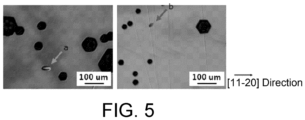
- the present inventors have now discovered that by allowing the SiC substrate to include a biaxially oriented SiC layer such that, in X-ray topography (XRT) measurement or optical microscope observation, the percentage of the number of BPDs such that the absolute value of an acute angle between a BPD extension direction and the [11-20] direction is 15° or less, with respect to the total number of BPDs, is controlled, it is possible to reduce breakings and cracks that occur during substrate processing such as grinding, polishing, and cutting.
- XRT X-ray topography
- the present invention provides the following aspects:
- a SiC substrate comprising a biaxially oriented SiC layer, wherein the SiC substrate and the biaxially oriented SiC layer have an off angle
- a SiC substrate comprising a biaxially oriented SiC layer, wherein the SiC substrate and the biaxially oriented SiC layer have an off angle
- the method using a previously produced polycrystalline substance as the orientation precursor layer 40 ingenuity such as making the surface of the polycrystalline substance sufficiently smooth in advance is necessary in order to enhance the adhesion between the polycrystalline substance and the SiC single crystal substrate 20. Therefore, the method of directly forming the orientation precursor layer 40 is preferred in view of cost.
- the method of placing a previously produced green body on the SiC single crystal substrate 20 is also preferred as a simple method, but the orientation precursor layer 40 is composed of a powder, and therefore a sintering process is necessary in the heat treatment process, which will be described later.
- the AD method is a technique such that fine particles or fine particle raw materials are mixed with a gas to form aerosol, and this aerosol is jetted at a high speed from a nozzle to allow the aerosol to collide with a substrate to form a coat and has a characteristic that the coat can be formed at normal temperature.
- Figure 3 shows an example of a film deposition apparatus (AD apparatus) that is used in such an AD method.
- An AD apparatus 50 shown in Figure 3 is configured as an apparatus that is used in an AD method in which a raw material powder is jetted onto a substrate in an atmosphere where the air pressure is lower than the atmospheric pressure.
- This AD apparatus 50 comprises: an aerosol generation unit 52 that generates aerosol of a raw material powder containing raw material components; and a film deposition unit 60 that jets the raw material powder onto the SiC single crystal substrate 20 to form a film containing the raw material components.
- the aerosol generation unit 52 comprises: an aerosol generation chamber 53 that receives supply of a carrier gas from a gas cylinder that stores the raw material powder, the gas cylinder not shown, to generate aerosol; a raw material supply pipe 54 that supplies generated aerosol to the film deposition unit 60; and a vibration exciter 55 that gives vibration of a frequency of 10 to 100 Hz to the aerosol generation chamber 53 and the aerosol therein.
- the film deposition unit 60 comprises: a film deposition chamber 62 that jets the aerosol onto the SiC single crystal substrate 20; a substrate holder 64 that is fixedly set up inside the film deposition chamber 62 to fix the SiC single crystal substrate 20; and an X-Y stage 63 that moves the substrate holder 64 in the X-axis and Y-axis directions. Further, the film deposition unit 60 comprises: a jet nozzle 66 that has a slit 67 formed at the tip and jets the aerosol onto the SiC single crystal substrate 20; and a vacuum pump 68 that reduces the pressure in the film deposition chamber 62. The jet nozzle 66 is attached to the tip of the raw material supply pipe 54.
- the AD method is known to generate pores in a film or make a film into a green compact depending on the film deposition conditions.
- the AD method is susceptible to the collision speed of the raw material powder onto the substrate, the particle size of the raw material powder, the aggregation state of the raw material powder in the aerosol, the jetting amount per unit time, and the like.
- the collision speed of the raw material powder onto the substrate is influenced by the differential pressure between the inside of the film deposition chamber 62 and the inside of the jet nozzle 66, the opening area of the jet nozzle, and the like. Therefore, to obtain a dense orientation precursor layer, these factors need to be controlled properly.
- known film deposition apparatuses such as commercially available film deposition apparatuses can be utilized as a film deposition apparatus.
- the raw material gas is not particularly limited, and a silicon tetrachloride (SiCl 4 ) gas and a silane (SiH 4 ) gas as a supply source of Si, and a methane (CH 4 ) gas, a propane (C 3 H 8 ) gas, and the like as a supply source of C can be used.
- the film deposition temperature is preferably 1000 to 2200°C, more preferably 1100 to 2000°C, and further preferably 1200 to 1900°C.
- the orientation precursor layer 40 is preferably not oriented, specifically is preferably an amorphous or non-oriented polycrystal, at the time of production, and it is preferred to allow rearrangement of the crystals to occur using a SiC single crystal as a seed crystal during the heat treatment process.
- the film deposition temperature, the flow rates of gases such as a Si source and a C source and the ratio thereof, the film deposition pressure, and the like are known to give influences in forming an amorphous or polycrystal layer on a SiC single crystal using the thermal CVD method.
- the film deposition temperature is preferably lower, preferably lower than 1700°C, more preferably 1500°C or lower, and further preferably 1400°C or lower.
- the film deposition temperature is preferably higher in view of the film deposition rate.
- the green body can be produced by forming a raw material powder for the orientation precursor.
- the orientation precursor layer 40 is a press-formed green body.
- the press-formed green body can be produced by subjecting the raw material powder for the orientation precursor to press forming based on a known method and may be produced by, for example, putting the raw material powder into a metal mold and pressing the raw material powder at a pressure of preferably 100 to 400 kgf/cm 2 , and more preferably 150 to 300 kgf/cm 2 .
- the forming method is not particularly limited, and tape casting, extrusion forming, slip casting, and a doctor blade method, and optional combinations thereof can be used in addition to press forming.
- additives such as a binder, a plasticizer, a dispersant, and a dispersion medium are appropriately added to the raw material powder to make a slurry, and this slurry is preferably allowed to pass through a slit-like thin ejection port to be ejected and formed into a sheet.
- the thickness of the green body formed into a sheet is not limited but is preferably 5 to 500 ⁇ m in view of handling.
- a plurality of the sheet green bodies may be stacked into a desired thickness for use. A portion of these green bodies near the SiC single crystal substrate 20 is made into the SiC substrate 30 by the subsequent heat treatment on the SiC single crystal substrate 20.
- the green bodies need to be sintered in the heat treatment process, which will be described later.
- the SiC substrate 30 is preferably formed after the green bodies are subjected to the process in which the green bodies are sintered and integrated as a polycrystalline substance with the SiC single crystal substrate 20.
- the green bodies do not undergo a sintered state, epitaxial growth using a SiC single crystal as a seed may occur insufficiently. Therefore, the green body may contain an additive such as a sintering aid in addition to the SiC raw material.
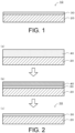
- a laminate in which the orientation precursor layers 40 are laminated or placed on the SiC single crystal substrate 20 are subjected to heat treatment to generate the SiC substrate 30.
- the heat treatment method is not particularly limited as long as epitaxial growth using the SiC single crystal substrate 20 as a seed occurs, and can be performed in a known heat treatment furnace such as a tube furnace or a hot plate. Not only heat treatment under normal pressure (pressless heat treatment) but also heat treatment under pressure such as hot pressing and HIP and a combination of the heat treatment under normal pressure and the heat treatment under pressure can be used.
- the atmosphere during the heat treatment can be selected from vacuum, nitrogen, and inert gas atmospheres, and combinations thereof.
- the concentration of N in the biaxially oriented SiC layer can be controlled by adjusting the amount of nitrogen in the atmosphere during the heat treatment.
- the heat treatment temperature is preferably 1700 to 2700°C.
- the orientation precursor layer 40 is likely to grow using the SiC single crystal substrate 20 as a seed crystal while being oriented along the c-axis and the a-axis. Therefore, the heat treatment temperature is preferably 1700°C or higher, more preferably 1800°C or higher, further preferably 1900°C or higher, and particularly preferably 2200°C or higher.
- the heat treatment temperature is preferably 2700°C or lower, and more preferably 2500°C or lower.
- the heat treatment conditions give an influence on the concentrations of the rare earth element, N, and B in the biaxially oriented SiC layer, and therefore it is preferred to appropriately control the conditions (for example, the heat treatment temperature and holding time). From such viewpoints, the heat treatment temperature is preferably 1900 to 2700°C, more preferably 2200 to 2600°C, and further preferably 2400 to 2500°C.
- the holding time is preferably 2 to 30 hours, and more preferably 4 to 20 hours.
- the heat treatment may be performed in a plurality of steps.
- the heat treatment may be performed under the condition in which heat treatment is performed in a nitrogen atmosphere at 1950°C for three hours, and then heat treatment is performed in an argon atmosphere at 2400°C for three hours.
- the heat treatment temperature and the total holding time are preferably within the above ranges.
- the heat treatment temperature and the holding time have a relationship with the thickness of the SiC substrate 30 generated by epitaxial growth and can be appropriately adjusted.
- a previously produced green body when used as the orientation precursor layer 40, needs to be sintered during the heat treatment, and normal pressure firing at a high temperature, hot pressing, HIP, or a combination thereof is suitable.
- the surface pressure is preferably 50 kgf/cm 2 or higher, more preferably 100 kgf/cm 2 or higher, and further preferably 200 kgf/cm 2 or higher, and there is no upper limit in particular.
- the firing temperature is not particularly limited as long as sintering and epitaxial growth occur.
- the firing conditions give an influence on the concentrations of the rare earth element, N, and B in the biaxially oriented SiC layer, and therefore it is preferred to appropriately control the conditions (for example, the firing temperature and holding time).
- the firing temperature is preferably 1700 to 2700°C.
- the holding time is preferably 2 to 18 hours.
- the atmosphere during the firing can be selected from vacuum, nitrogen, and inert gas atmospheres, or a mixed gas of nitrogen and an inert gas.
- the firing may be performed in a plurality of steps, and the firing temperature and the total holding time are preferably within the above range.
- the SiC powder which is a raw material may be composed of at least one of an ⁇ -SiC powder and a ⁇ -SiC powder, but the SiC powder is preferably composed of a ⁇ -SiC powder.
- the SiC powder is preferably composed of SiC particles having an average particle size of 0.01 to 100 ⁇ m.
- the average particle size refers to an average value obtained when the powder is observed with a scanning electron microscope to measure the maximum sizes in a constant direction for 100 primary particles.
- the crystals in the orientation precursor layer 40 grow while being oriented along the c-axis and the a-axis from the crystal growth surface of the SiC single crystal substrate 20, and therefore the orientation precursor layer 40 is gradually changed into the SiC substrate 30 from the crystal growth surface.
- the SiC composite substrate comprising the generated SiC substrate 30 is such that breakings and cracks that occur during substrate processing are reduced.
- the orientation precursor layer 40 left on the SiC substrate 30 after the heat treatment process is ground away to expose the surface of the SiC substrate 30, and the exposed surface is subjected to grinding and/or polishing.
- the SiC composite substrate 10 is obtained.
- the present invention is not limited to the above-described embodiments, and it is needless to say that that the present invention can be conducted in various aspects as long as they belong to the technical scope of the present invention.
- only one layer of the SiC substrate 30 is provided on the SiC single crystal substrate 20, but two or more layers may be provided.
- the SiC substrate 30 as the second layer can be provided on the SiC substrate 30.
- a raw material powder containing 90.8% by weight of a commercially available ⁇ -SiC fine powder (volume-based D50 particle size: 0.7 ⁇ m), 8.1% by weight of an yttrium oxide powder (volume-based D50 particle size: 0.1 ⁇ m), and 1.1% by weight of a silicon dioxide powder (volume-based D50 particle size: 0.7 ⁇ m) was provided.
- This raw material powder was mixed with a ball mill using SiC balls in ethanol for 24 hours, and the resultant mixture was dried to obtain a mixed powder.
- Conditions for depositing the AD film were as follows. Firstly, He was used as a carrier gas, and the film was deposited using a nozzle made of a ceramic and being such that a slit of 5 mm in long side ⁇ 0.4 mm in short side was formed. The condition for scanning the nozzle was as follows.
- the SiC single crystal substrate on which the AD film, which is the orientation precursor layer was formed was taken out of the AD apparatus, and annealed in an argon atmosphere at 2400°C for 10 hours.
- the orientation precursor layer was subjected to heat treatment to form a heat-treated layer.
- a (000-1) plane of the SiC single crystal substrate including a heat-treated layer formed thereon was subjected to surface grinding with a grinder (diamond wheel of #1000 to 6000) to a predetermined thickness to achieve a targeted thickness and surface state.
- a SiC substrate was obtained.
- the magnification of the eyepiece lens was set to 10x, and the magnification of the objective lens was set to 5x.
- the entire surface of the SiC substrate obtained in (3) was observed in the polarizing mode and the differential interference contrast mode, and if breakings and cracks were found in the substrate, the substrate was regarded as a substrate having breakings and cracks. At this time, only breakings and cracks having a length of 100 ⁇ m or more were counted as breakings and cracks.
- a SiC substrate was produced and evaluated as in Example 1 except that a raw material powder containing 88.8% by weight of the ⁇ -SiC fine powder (volume-based D50 particle size: 0.7 ⁇ m), 8.1% by weight of the yttrium oxide powder (volume-based D50 particle size: 0.1 ⁇ m), 1.1% by weight of the silicon dioxide powder (volume-based D50 particle size: 0.7 ⁇ m), and 2.0% by weight of the boron carbide powder (volume-based D50 particle size: 0.5 ⁇ m) was used in (1).
- the resultant heat-treated layer was confirmed to be a biaxially oriented SiC layer. The results were as shown in Table 1.
- a SiC substrate was produced and evaluated as in Example 1 except that a raw material powder containing 86.8% by weight of the ⁇ -SiC fine powder (volume-based D50 particle size: 0.7 ⁇ m), 8.1% by weight of the yttrium oxide powder (volume-based D50 particle size: 0.1 ⁇ m), 1.1% by weight of the silicon dioxide powder (volume-based D50 particle size: 0.7 ⁇ m), and 4.0% by weight of the boron carbide powder (volume-based D50 particle size: 0.5 ⁇ m) was used in (1).
- the resultant heat-treated layer was confirmed to be a biaxially oriented SiC layer. The results were as shown in Table 1.
- a SiC substrate was produced and evaluated as in Example 1 except that the heat treatment atmosphere was set to 99.5% of argon and 0.5% of nitrogen in (2).
- the resultant heat-treated layer was confirmed to be a biaxially oriented SiC layer. The results were as shown in Table 1.
- a rare earth element concentration is 5.0 ⁇ 10 14 to 5.0 ⁇ 10 15 atoms/cm 3
- a N concentration is 1.0 ⁇ 10 18 to 2.0 ⁇ 10 19 atoms/cm 3
- a B concentration is 2.0 ⁇ 10 15 to 1.0 ⁇ 10 17 atoms/cm 3 .
Landscapes
- Chemical & Material Sciences (AREA)
- Engineering & Computer Science (AREA)
- Crystallography & Structural Chemistry (AREA)
- Materials Engineering (AREA)
- Metallurgy (AREA)
- Organic Chemistry (AREA)
- Inorganic Chemistry (AREA)
- Physics & Mathematics (AREA)
- Thermal Sciences (AREA)
- Crystals, And After-Treatments Of Crystals (AREA)
Applications Claiming Priority (1)
| Application Number | Priority Date | Filing Date | Title |
|---|---|---|---|
| PCT/JP2022/031636 WO2024042591A1 (ja) | 2022-08-22 | 2022-08-22 | SiC基板及びSiC複合基板 |
Publications (1)
| Publication Number | Publication Date |
|---|---|
| EP4579006A1 true EP4579006A1 (en) | 2025-07-02 |
Family
ID=90012690
Family Applications (1)
| Application Number | Title | Priority Date | Filing Date |
|---|---|---|---|
| EP22956419.0A Pending EP4579006A1 (en) | 2022-08-22 | 2022-08-22 | Sic substrate and sic composite substrate |
Country Status (5)
| Country | Link |
|---|---|
| US (1) | US20250126865A1 (https=) |
| EP (1) | EP4579006A1 (https=) |
| JP (1) | JP7686016B2 (https=) |
| CN (1) | CN119654452A (https=) |
| WO (1) | WO2024042591A1 (https=) |
Family Cites Families (6)
| Publication number | Priority date | Publication date | Assignee | Title |
|---|---|---|---|---|
| JP2014162649A (ja) | 2013-02-21 | 2014-09-08 | Mitsubishi Electric Corp | SiC基板、SiC基板の製造方法、SiCエピタキシャル基板 |
| JP6968408B2 (ja) | 2017-07-20 | 2021-11-17 | 国立大学法人東海国立大学機構 | 炭化ケイ素単結晶の製造方法 |
| JP7422479B2 (ja) * | 2017-12-22 | 2024-01-26 | 株式会社レゾナック | SiCインゴット及びSiCインゴットの製造方法 |
| WO2020195196A1 (ja) * | 2019-03-27 | 2020-10-01 | 日本碍子株式会社 | SiC複合基板及び半導体デバイス用複合基板 |
| WO2020255343A1 (ja) * | 2019-06-20 | 2020-12-24 | 三菱電機株式会社 | 炭化ケイ素単結晶、半導体素子 |
| WO2022168372A1 (ja) | 2021-02-05 | 2022-08-11 | 日本碍子株式会社 | 希土類含有SiC基板及びそれを用いたSiC複合基板 |
-
2022
- 2022-08-22 EP EP22956419.0A patent/EP4579006A1/en active Pending
- 2022-08-22 WO PCT/JP2022/031636 patent/WO2024042591A1/ja not_active Ceased
- 2022-08-22 CN CN202280095382.3A patent/CN119654452A/zh active Pending
- 2022-08-22 JP JP2022579778A patent/JP7686016B2/ja active Active
-
2024
- 2024-12-20 US US18/989,246 patent/US20250126865A1/en active Pending
Also Published As
| Publication number | Publication date |
|---|---|
| CN119654452A (zh) | 2025-03-18 |
| JPWO2024042591A1 (https=) | 2024-02-29 |
| WO2024042591A1 (ja) | 2024-02-29 |
| JP7686016B2 (ja) | 2025-05-30 |
| US20250126865A1 (en) | 2025-04-17 |
Similar Documents
| Publication | Publication Date | Title |
|---|---|---|
| US12125883B2 (en) | Biaxially oriented SiC composite substrate and semiconductor device composite substrate | |
| US12424440B2 (en) | Rare earth-containing SiC substrate and method for producing SiC epitaxial layer | |
| CN113574215A (zh) | 基底基板及其制造方法 | |
| JP7538900B2 (ja) | 希土類含有SiC基板及びそれを用いたSiC複合基板 | |
| US12080551B2 (en) | SiC composite substrate including biaxially oreinted SiC layer and semiconductor device | |
| US12421621B2 (en) | Underlying substrate | |
| US20240186380A1 (en) | SiC SUBSTRATE SiC COMPOSITE SUBSTRATE | |
| WO2023062850A1 (ja) | 希土類含有SiC基板及びSiC複合基板 | |
| EP4579006A1 (en) | Sic substrate and sic composite substrate | |
| EP4692430A1 (en) | Sic substrate and sic composite substrate | |
| US20260043171A1 (en) | SiC SUBSTRATE AND SiC COMPOSITE SUBSTRATE | |
| US20240250127A1 (en) | RARE EARTH-CONTAINING SiC SUBSTRATE AND SiC COMPOSITE SUBSTRATE | |
| US20250391657A1 (en) | Base substrate | |
| WO2025083939A1 (ja) | SiC基板及びSiC複合基板 |
Legal Events
| Date | Code | Title | Description |
|---|---|---|---|
| STAA | Information on the status of an ep patent application or granted ep patent |
Free format text: STATUS: THE INTERNATIONAL PUBLICATION HAS BEEN MADE |
|
| PUAI | Public reference made under article 153(3) epc to a published international application that has entered the european phase |
Free format text: ORIGINAL CODE: 0009012 |
|
| STAA | Information on the status of an ep patent application or granted ep patent |
Free format text: STATUS: REQUEST FOR EXAMINATION WAS MADE |
|
| 17P | Request for examination filed |
Effective date: 20250123 |
|
| AK | Designated contracting states |
Kind code of ref document: A1 Designated state(s): AL AT BE BG CH CY CZ DE DK EE ES FI FR GB GR HR HU IE IS IT LI LT LU LV MC MK MT NL NO PL PT RO RS SE SI SK SM TR |
|
| DAV | Request for validation of the european patent (deleted) | ||
| DAX | Request for extension of the european patent (deleted) |