EP4579005A1 - Sic-ingot und verfahren zur herstellung eines sic-substrats - Google Patents
Sic-ingot und verfahren zur herstellung eines sic-substrats Download PDFInfo
- Publication number
- EP4579005A1 EP4579005A1 EP24210035.2A EP24210035A EP4579005A1 EP 4579005 A1 EP4579005 A1 EP 4579005A1 EP 24210035 A EP24210035 A EP 24210035A EP 4579005 A1 EP4579005 A1 EP 4579005A1
- Authority
- EP
- European Patent Office
- Prior art keywords
- sic
- sic ingot
- inclined surface
- growth
- ingot
- Prior art date
- Legal status (The legal status is an assumption and is not a legal conclusion. Google has not performed a legal analysis and makes no representation as to the accuracy of the status listed.)
- Pending
Links
Images

Classifications
-
- C—CHEMISTRY; METALLURGY
- C30—CRYSTAL GROWTH
- C30B—SINGLE-CRYSTAL GROWTH; UNIDIRECTIONAL SOLIDIFICATION OF EUTECTIC MATERIAL OR UNIDIRECTIONAL DEMIXING OF EUTECTOID MATERIAL; REFINING BY ZONE-MELTING OF MATERIAL; PRODUCTION OF A HOMOGENEOUS POLYCRYSTALLINE MATERIAL WITH DEFINED STRUCTURE; SINGLE CRYSTALS OR HOMOGENEOUS POLYCRYSTALLINE MATERIAL WITH DEFINED STRUCTURE; AFTER-TREATMENT OF SINGLE CRYSTALS OR A HOMOGENEOUS POLYCRYSTALLINE MATERIAL WITH DEFINED STRUCTURE; APPARATUS THEREFOR
- C30B29/00—Single crystals or homogeneous polycrystalline material with defined structure characterised by the material or by their shape
- C30B29/10—Inorganic compounds or compositions
- C30B29/36—Carbides
-
- B—PERFORMING OPERATIONS; TRANSPORTING
- B28—WORKING CEMENT, CLAY, OR STONE
- B28D—WORKING STONE OR STONE-LIKE MATERIALS
- B28D5/00—Fine working of gems, jewels, crystals, e.g. of semiconductor material; apparatus or devices therefor
- B28D5/0005—Fine working of gems, jewels, crystals, e.g. of semiconductor material; apparatus or devices therefor by breaking, e.g. dicing
- B28D5/0011—Fine working of gems, jewels, crystals, e.g. of semiconductor material; apparatus or devices therefor by breaking, e.g. dicing with preliminary treatment, e.g. weakening by scoring
-
- B—PERFORMING OPERATIONS; TRANSPORTING
- B28—WORKING CEMENT, CLAY, OR STONE
- B28D—WORKING STONE OR STONE-LIKE MATERIALS
- B28D5/00—Fine working of gems, jewels, crystals, e.g. of semiconductor material; apparatus or devices therefor
- B28D5/04—Fine working of gems, jewels, crystals, e.g. of semiconductor material; apparatus or devices therefor by tools other than rotary type, e.g. reciprocating tools
-
- B—PERFORMING OPERATIONS; TRANSPORTING
- B28—WORKING CEMENT, CLAY, OR STONE
- B28D—WORKING STONE OR STONE-LIKE MATERIALS
- B28D5/00—Fine working of gems, jewels, crystals, e.g. of semiconductor material; apparatus or devices therefor
- B28D5/04—Fine working of gems, jewels, crystals, e.g. of semiconductor material; apparatus or devices therefor by tools other than rotary type, e.g. reciprocating tools
- B28D5/045—Fine working of gems, jewels, crystals, e.g. of semiconductor material; apparatus or devices therefor by tools other than rotary type, e.g. reciprocating tools by cutting with wires or closed-loop blades
-
- C—CHEMISTRY; METALLURGY
- C30—CRYSTAL GROWTH
- C30B—SINGLE-CRYSTAL GROWTH; UNIDIRECTIONAL SOLIDIFICATION OF EUTECTIC MATERIAL OR UNIDIRECTIONAL DEMIXING OF EUTECTOID MATERIAL; REFINING BY ZONE-MELTING OF MATERIAL; PRODUCTION OF A HOMOGENEOUS POLYCRYSTALLINE MATERIAL WITH DEFINED STRUCTURE; SINGLE CRYSTALS OR HOMOGENEOUS POLYCRYSTALLINE MATERIAL WITH DEFINED STRUCTURE; AFTER-TREATMENT OF SINGLE CRYSTALS OR A HOMOGENEOUS POLYCRYSTALLINE MATERIAL WITH DEFINED STRUCTURE; APPARATUS THEREFOR
- C30B23/00—Single-crystal growth by condensing evaporated or sublimed materials
-
- C—CHEMISTRY; METALLURGY
- C30—CRYSTAL GROWTH
- C30B—SINGLE-CRYSTAL GROWTH; UNIDIRECTIONAL SOLIDIFICATION OF EUTECTIC MATERIAL OR UNIDIRECTIONAL DEMIXING OF EUTECTOID MATERIAL; REFINING BY ZONE-MELTING OF MATERIAL; PRODUCTION OF A HOMOGENEOUS POLYCRYSTALLINE MATERIAL WITH DEFINED STRUCTURE; SINGLE CRYSTALS OR HOMOGENEOUS POLYCRYSTALLINE MATERIAL WITH DEFINED STRUCTURE; AFTER-TREATMENT OF SINGLE CRYSTALS OR A HOMOGENEOUS POLYCRYSTALLINE MATERIAL WITH DEFINED STRUCTURE; APPARATUS THEREFOR
- C30B23/00—Single-crystal growth by condensing evaporated or sublimed materials
- C30B23/02—Epitaxial-layer growth
-
- C—CHEMISTRY; METALLURGY
- C30—CRYSTAL GROWTH
- C30B—SINGLE-CRYSTAL GROWTH; UNIDIRECTIONAL SOLIDIFICATION OF EUTECTIC MATERIAL OR UNIDIRECTIONAL DEMIXING OF EUTECTOID MATERIAL; REFINING BY ZONE-MELTING OF MATERIAL; PRODUCTION OF A HOMOGENEOUS POLYCRYSTALLINE MATERIAL WITH DEFINED STRUCTURE; SINGLE CRYSTALS OR HOMOGENEOUS POLYCRYSTALLINE MATERIAL WITH DEFINED STRUCTURE; AFTER-TREATMENT OF SINGLE CRYSTALS OR A HOMOGENEOUS POLYCRYSTALLINE MATERIAL WITH DEFINED STRUCTURE; APPARATUS THEREFOR
- C30B23/00—Single-crystal growth by condensing evaporated or sublimed materials
- C30B23/02—Epitaxial-layer growth
- C30B23/06—Heating of the deposition chamber, the substrate or the materials to be evaporated
-
- C—CHEMISTRY; METALLURGY
- C30—CRYSTAL GROWTH
- C30B—SINGLE-CRYSTAL GROWTH; UNIDIRECTIONAL SOLIDIFICATION OF EUTECTIC MATERIAL OR UNIDIRECTIONAL DEMIXING OF EUTECTOID MATERIAL; REFINING BY ZONE-MELTING OF MATERIAL; PRODUCTION OF A HOMOGENEOUS POLYCRYSTALLINE MATERIAL WITH DEFINED STRUCTURE; SINGLE CRYSTALS OR HOMOGENEOUS POLYCRYSTALLINE MATERIAL WITH DEFINED STRUCTURE; AFTER-TREATMENT OF SINGLE CRYSTALS OR A HOMOGENEOUS POLYCRYSTALLINE MATERIAL WITH DEFINED STRUCTURE; APPARATUS THEREFOR
- C30B29/00—Single crystals or homogeneous polycrystalline material with defined structure characterised by the material or by their shape
- C30B29/60—Single crystals or homogeneous polycrystalline material with defined structure characterised by the material or by their shape characterised by shape
- C30B29/66—Crystals of complex geometrical shape, e.g. tubes, cylinders
-
- C—CHEMISTRY; METALLURGY
- C30—CRYSTAL GROWTH
- C30B—SINGLE-CRYSTAL GROWTH; UNIDIRECTIONAL SOLIDIFICATION OF EUTECTIC MATERIAL OR UNIDIRECTIONAL DEMIXING OF EUTECTOID MATERIAL; REFINING BY ZONE-MELTING OF MATERIAL; PRODUCTION OF A HOMOGENEOUS POLYCRYSTALLINE MATERIAL WITH DEFINED STRUCTURE; SINGLE CRYSTALS OR HOMOGENEOUS POLYCRYSTALLINE MATERIAL WITH DEFINED STRUCTURE; AFTER-TREATMENT OF SINGLE CRYSTALS OR A HOMOGENEOUS POLYCRYSTALLINE MATERIAL WITH DEFINED STRUCTURE; APPARATUS THEREFOR
- C30B33/00—After-treatment of single crystals or homogeneous polycrystalline material with defined structure
-
- C—CHEMISTRY; METALLURGY
- C30—CRYSTAL GROWTH
- C30B—SINGLE-CRYSTAL GROWTH; UNIDIRECTIONAL SOLIDIFICATION OF EUTECTIC MATERIAL OR UNIDIRECTIONAL DEMIXING OF EUTECTOID MATERIAL; REFINING BY ZONE-MELTING OF MATERIAL; PRODUCTION OF A HOMOGENEOUS POLYCRYSTALLINE MATERIAL WITH DEFINED STRUCTURE; SINGLE CRYSTALS OR HOMOGENEOUS POLYCRYSTALLINE MATERIAL WITH DEFINED STRUCTURE; AFTER-TREATMENT OF SINGLE CRYSTALS OR A HOMOGENEOUS POLYCRYSTALLINE MATERIAL WITH DEFINED STRUCTURE; APPARATUS THEREFOR
- C30B33/00—After-treatment of single crystals or homogeneous polycrystalline material with defined structure
- C30B33/06—Joining of crystals
-
- G—PHYSICS
- G01—MEASURING; TESTING
- G01N—INVESTIGATING OR ANALYSING MATERIALS BY DETERMINING THEIR CHEMICAL OR PHYSICAL PROPERTIES
- G01N33/00—Investigating or analysing materials by specific methods not covered by groups G01N1/00 - G01N31/00
- G01N33/0095—Semiconductive materials
Definitions
- the present invention relates to a SiC ingot and a method for manufacturing a SiC substrate.
- Silicon carbide (SiC) has a dielectric breakdown field one order of magnitude larger than silicon (Si) and a band gap three times larger than silicon (Si).
- silicon carbide (SiC) has properties such as a thermal conductivity about three times higher than silicon (Si). For this reason, silicon carbide (SiC) is expected to be applied to power devices, high frequency devices, high temperature operating devices, and the like. For this reason, in recent years, SiC epitaxial wafers have come to be used for the above-described semiconductor devices.
- a SiC epitaxial wafer is obtained by stacking a SiC epitaxial layer on the surface of a SiC substrate.
- the substrate before the SiC epitaxial layer is stacked thereon is referred to as a SiC substrate
- the substrate after the SiC epitaxial layer is stacked thereon is referred to as a SiC epitaxial wafer.
- the SiC substrate is cut out from a SiC ingot.
- a SiC ingot is obtained by performing crystal growth of a SiC single crystal on a seed crystal.
- Patent Document 1 when a SiC ingot is produced, facets are formed in the SiC ingot.
- a part of a crystal growth surface becomes parallel to a c plane, and a surface parallel to the c plane is exposed on the crystal growth surface.
- This surface parallel to the c plane has a different pattern in crystal growth from other crystal growth surfaces on which step-flow growth is performed.
- a portion obtained through the crystal growth in a different pattern from a portion obtained through the step-flow growth is a facet.
- Patent Document 1 Japanese Patent No. 6050053
- the facet has a lower resistance value than the portion obtained through the step-flow growth. This is because the amount of nitrogen taken in is relatively increased on the facet.
- a difference in resistivity between the facet and a step-flow growth region adversely affects laser processing and electric discharge processing. For example, in a case in which cracks are created in a SiC ingot with a laser and a SiC substrate is cut out from the SiC ingot, it is necessary to change a laser output at a boundary between the facet and the step-flow growth region. The greater the number of times that the laser output is changed, the lower the throughput of the processing. On the other hand, if the facet becomes too small, especially in the early stages of growth, threading screw dislocations (TSDs) cannot be sufficiently introduced into the facet, and thus heterogeneous polymorphs are likely to occur.
- TSDs threading screw dislocations
- the present invention has been made in consideration of the above-described problems, and an object of the present invention is to provide a SiC ingot for achieving both crystal quality and easiness of processing and a method for manufacturing a SiC substrate using the SiC ingot.
- the present invention provides the following solutions to solve the above problems.
- the boundary between the facet 4 and the step-flow growth region 5 can be determined visually, but may also be determined by the following procedure.
- First, an image of a cut surface to be measured is acquired.
- the image is acquired by polishing both surfaces of the substrate and using a scanner.
- As the scanner for example, a flatbed scanner manufactured by Canon Inc. can be used.
- the acquired image is converted into an HLS color space consisting of hue, luminance, and saturation, and the luminance is calculated.
- a circle of pixels with a radius X is drawn with an arbitrary pixel as the center of the circle.
- the SiC ingot of Comparative Example 3 was produced. Then, the cross section of the produced SiC ingot was checked, and the shape of the inner boundary between the facet and the step-flow growth region was checked.
- the inner boundary included the first inclined surface and the second inclined surface. The inflection point between the first inclined surface and the second inclined surface was located at a position shifted by 80% of the ingot length in the Z direction from the first end.
- the quality yield of the SiC ingots in Comparative Example 3 was 95%.
- the time required to slice the SiC ingots of Comparative Example 3 into wafers was 19.5 minutes per wafer.
- the process in which the growth of the SiC ingot was progressed to 70% of the final growth amount was defined as the first growth process, and the process in which the growth of the SiC ingot was progressed from 70% of the final growth amount to the end was defined as the second growth process.
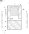
- the position of the heat insulating member 22 in the Z direction was set to 5 mm above the center position of the crystal growth surface for the SiC ingot during the first growth process, and the position of the heat insulating member 22 in the Z direction was set to 5 mm below the center position of the crystal growth surface for the SiC ingot during the second growth process.
- the inclination angle ⁇ of the inner side surface of the guide member 23 located on the offset upstream side was set to 70° at a position to 70% of the final growth amount of the SiC ingot (the position in the Z direction of the crystal growth surface in the first growth process) and was set to 85° at a position from 70% to 100% of the final growth amount of the SiC ingot (the position in the Z direction of the crystal growth surface in the second growth process).
- Other conditions were the same as those in Example 1 and the SiC ingot of Comparative Example 4 was produced.
- the cross section of the produced SiC ingot was checked, and the shape of the inner boundary between the facet and the step-flow growth region was checked.
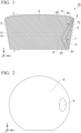
- the SiC ingot included a first end that was opposite the growth surface of the seed crystal and a second end that was the growth surface.
- the inner boundary of the facet included the first inclined surface and the second inclined surface.
- the first inclined surface was closer to the first end than the second inclined surface.
- the inclination angle of the first inclined surface with respect to the crystal growth direction was larger than the inclination angle of the second inclined surface with respect to the crystal growth direction.
- the first inclined surface included a portion in which an absolute value of an inclination angle with respect to the crystal growth direction was 5° or more.
- the second inclined surface did not include a portion in which an absolute value of an inclination angle with respect to the crystal growth direction was 15° or more.
- the inflection point between the first inclined surface and the second inclined surface was located at a position shifted by 60% of the ingot length in the Z direction from the first end.
- the facet was located in a [11-20] direction from a plane that passed through a center in a ⁇ 11-20> direction and was orthogonal to the ⁇ 11-20> direction.
Landscapes
- Chemical & Material Sciences (AREA)
- Engineering & Computer Science (AREA)
- Crystallography & Structural Chemistry (AREA)
- Materials Engineering (AREA)
- Metallurgy (AREA)
- Organic Chemistry (AREA)
- Mechanical Engineering (AREA)
- Inorganic Chemistry (AREA)
- Health & Medical Sciences (AREA)
- Life Sciences & Earth Sciences (AREA)
- Physics & Mathematics (AREA)
- Medicinal Chemistry (AREA)
- Analytical Chemistry (AREA)
- Biochemistry (AREA)
- General Health & Medical Sciences (AREA)
- General Physics & Mathematics (AREA)
- Immunology (AREA)
- Pathology (AREA)
- Food Science & Technology (AREA)
- Geometry (AREA)
- Crystals, And After-Treatments Of Crystals (AREA)
Applications Claiming Priority (6)
| Application Number | Priority Date | Filing Date | Title |
|---|---|---|---|
| JP2023223451 | 2023-12-28 | ||
| JP2023223461 | 2023-12-28 | ||
| JP2023223189 | 2023-12-28 | ||
| JP2024188125A JP7852690B2 (ja) | 2023-12-28 | 2024-10-25 | SiCインゴット及びSiC基板の製造方法 |
| JP2024188277A JP2025105457A (ja) | 2023-12-28 | 2024-10-25 | SiCインゴット及びSiC基板の製造方法 |
| JP2024188186A JP7852691B2 (ja) | 2023-12-28 | 2024-10-25 | SiCインゴット、SiC基板の製造方法およびSiCインゴットの評価方法 |
Publications (1)
| Publication Number | Publication Date |
|---|---|
| EP4579005A1 true EP4579005A1 (de) | 2025-07-02 |
Family
ID=93376427
Family Applications (3)
| Application Number | Title | Priority Date | Filing Date |
|---|---|---|---|
| EP24210073.3A Pending EP4589056A1 (de) | 2023-12-28 | 2024-10-31 | Sic-ingot und verfahren zur herstellung eines sic-substrats |
| EP24210031.1A Pending EP4579004A1 (de) | 2023-12-28 | 2024-10-31 | Sic-ingot und verfahren zur herstellung eines sic-substrats |
| EP24210035.2A Pending EP4579005A1 (de) | 2023-12-28 | 2024-10-31 | Sic-ingot und verfahren zur herstellung eines sic-substrats |
Family Applications Before (2)
| Application Number | Title | Priority Date | Filing Date |
|---|---|---|---|
| EP24210073.3A Pending EP4589056A1 (de) | 2023-12-28 | 2024-10-31 | Sic-ingot und verfahren zur herstellung eines sic-substrats |
| EP24210031.1A Pending EP4579004A1 (de) | 2023-12-28 | 2024-10-31 | Sic-ingot und verfahren zur herstellung eines sic-substrats |
Country Status (4)
| Country | Link |
|---|---|
| US (3) | US20250215612A1 (de) |
| EP (3) | EP4589056A1 (de) |
| KR (3) | KR20250103414A (de) |
| CN (3) | CN120231130A (de) |
Citations (5)
| Publication number | Priority date | Publication date | Assignee | Title |
|---|---|---|---|---|
| JP6050053B2 (ja) | 2012-08-23 | 2016-12-21 | 株式会社豊田中央研究所 | SiC単結晶の製造方法 |
| US20170342593A1 (en) * | 2014-12-05 | 2017-11-30 | Nippon Steel & Sumitomo Metal Corporation | Method for producing silicon carbide single crystal and silicon carbide single crystal substrate |
| US10236338B2 (en) * | 2015-04-21 | 2019-03-19 | Showa Denko K.K. | SiC single crystal seed, SiC ingot, SiC single crystal seed production method, and SiC single crystal ingot production method |
| JP6722578B2 (ja) * | 2016-12-26 | 2020-07-15 | 昭和電工株式会社 | SiCウェハの製造方法 |
| JP7038756B2 (ja) * | 2020-05-29 | 2022-03-18 | 昭和電工株式会社 | SiCウェハ及び半導体デバイスの製造方法 |
Family Cites Families (2)
| Publication number | Priority date | Publication date | Assignee | Title |
|---|---|---|---|---|
| JP5803265B2 (ja) * | 2011-05-20 | 2015-11-04 | 住友電気工業株式会社 | 炭化珪素基板および炭化珪素インゴットの製造方法 |
| US10562130B1 (en) * | 2018-12-29 | 2020-02-18 | Cree, Inc. | Laser-assisted method for parting crystalline material |
-
2024
- 2024-10-29 KR KR1020240149563A patent/KR20250103414A/ko active Pending
- 2024-10-29 KR KR1020240149573A patent/KR20250103415A/ko active Pending
- 2024-10-29 KR KR1020240149593A patent/KR20250103416A/ko active Pending
- 2024-10-31 US US18/933,285 patent/US20250215612A1/en active Pending
- 2024-10-31 CN CN202411538224.8A patent/CN120231130A/zh active Pending
- 2024-10-31 CN CN202411537913.7A patent/CN120231129A/zh active Pending
- 2024-10-31 US US18/932,740 patent/US20250215610A1/en active Pending
- 2024-10-31 CN CN202411538342.9A patent/CN120231131A/zh active Pending
- 2024-10-31 US US18/932,748 patent/US20250215611A1/en active Pending
- 2024-10-31 EP EP24210073.3A patent/EP4589056A1/de active Pending
- 2024-10-31 EP EP24210031.1A patent/EP4579004A1/de active Pending
- 2024-10-31 EP EP24210035.2A patent/EP4579005A1/de active Pending
Patent Citations (5)
| Publication number | Priority date | Publication date | Assignee | Title |
|---|---|---|---|---|
| JP6050053B2 (ja) | 2012-08-23 | 2016-12-21 | 株式会社豊田中央研究所 | SiC単結晶の製造方法 |
| US20170342593A1 (en) * | 2014-12-05 | 2017-11-30 | Nippon Steel & Sumitomo Metal Corporation | Method for producing silicon carbide single crystal and silicon carbide single crystal substrate |
| US10236338B2 (en) * | 2015-04-21 | 2019-03-19 | Showa Denko K.K. | SiC single crystal seed, SiC ingot, SiC single crystal seed production method, and SiC single crystal ingot production method |
| JP6722578B2 (ja) * | 2016-12-26 | 2020-07-15 | 昭和電工株式会社 | SiCウェハの製造方法 |
| JP7038756B2 (ja) * | 2020-05-29 | 2022-03-18 | 昭和電工株式会社 | SiCウェハ及び半導体デバイスの製造方法 |
Also Published As
| Publication number | Publication date |
|---|---|
| KR20250103415A (ko) | 2025-07-07 |
| US20250215611A1 (en) | 2025-07-03 |
| CN120231130A (zh) | 2025-07-01 |
| KR20250103416A (ko) | 2025-07-07 |
| KR20250103414A (ko) | 2025-07-07 |
| EP4589056A1 (de) | 2025-07-23 |
| CN120231131A (zh) | 2025-07-01 |
| EP4579004A1 (de) | 2025-07-02 |
| CN120231129A (zh) | 2025-07-01 |
| US20250215612A1 (en) | 2025-07-03 |
| US20250215610A1 (en) | 2025-07-03 |
Similar Documents
| Publication | Publication Date | Title |
|---|---|---|
| JP7817163B2 (ja) | 大口径炭化ケイ素ウェハ | |
| US20250006491A1 (en) | Large dimension silicon carbide single crystalline materials with reduced crystallographic stress | |
| JP2024522507A (ja) | シリコンカーバイド結晶性材料のための光吸収の低減 | |
| EP4579005A1 (de) | Sic-ingot und verfahren zur herstellung eines sic-substrats | |
| JP7852690B2 (ja) | SiCインゴット及びSiC基板の製造方法 | |
| US11705329B2 (en) | SiC epitaxial wafer and method for manufacturing same | |
| JP7852691B2 (ja) | SiCインゴット、SiC基板の製造方法およびSiCインゴットの評価方法 | |
| EP4286565A1 (de) | Sic-substrat und sic-ingot | |
| US20250263868A1 (en) | Gallium nitride single crystal substrate and method for producing the same | |
| EP4286566A1 (de) | Sic-substrat und sic-ingot | |
| JP7214032B1 (ja) | SiCデバイスの製造方法 | |
| EP4527992A2 (de) | Sic-einkristallkugel, herstellungsverfahren für sic-einkristallkugel und herstellungsverfahren für sic-substrat | |
| JP2025105457A (ja) | SiCインゴット及びSiC基板の製造方法 | |
| US12480226B2 (en) | AlN single crystal substrate | |
| US20260009158A1 (en) | Ain single crystal substrate and device |
Legal Events
| Date | Code | Title | Description |
|---|---|---|---|
| PUAI | Public reference made under article 153(3) epc to a published international application that has entered the european phase |
Free format text: ORIGINAL CODE: 0009012 |
|
| STAA | Information on the status of an ep patent application or granted ep patent |
Free format text: STATUS: REQUEST FOR EXAMINATION WAS MADE |
|
| 17P | Request for examination filed |
Effective date: 20241129 |
|
| AK | Designated contracting states |
Kind code of ref document: A1 Designated state(s): AL AT BE BG CH CY CZ DE DK EE ES FI FR GB GR HR HU IE IS IT LI LT LU LV MC ME MK MT NL NO PL PT RO RS SE SI SK SM TR |