EP4577027A1 - Thermoelectric conversion module - Google Patents
Thermoelectric conversion module Download PDFInfo
- Publication number
- EP4577027A1 EP4577027A1 EP23862969.5A EP23862969A EP4577027A1 EP 4577027 A1 EP4577027 A1 EP 4577027A1 EP 23862969 A EP23862969 A EP 23862969A EP 4577027 A1 EP4577027 A1 EP 4577027A1
- Authority
- EP
- European Patent Office
- Prior art keywords
- thermoelectric conversion
- capacitor
- conversion element
- thermal conduction
- thickness direction
- Prior art date
- Legal status (The legal status is an assumption and is not a legal conclusion. Google has not performed a legal analysis and makes no representation as to the accuracy of the status listed.)
- Withdrawn
Links
Images



Classifications
-
- H—ELECTRICITY
- H10—SEMICONDUCTOR DEVICES; ELECTRIC SOLID-STATE DEVICES NOT OTHERWISE PROVIDED FOR
- H10N—ELECTRIC SOLID-STATE DEVICES NOT OTHERWISE PROVIDED FOR
- H10N10/00—Thermoelectric devices comprising a junction of dissimilar materials, i.e. devices exhibiting Seebeck or Peltier effects
- H10N10/10—Thermoelectric devices comprising a junction of dissimilar materials, i.e. devices exhibiting Seebeck or Peltier effects operating with only the Peltier or Seebeck effects
- H10N10/17—Thermoelectric devices comprising a junction of dissimilar materials, i.e. devices exhibiting Seebeck or Peltier effects operating with only the Peltier or Seebeck effects characterised by the structure or configuration of the cell or thermocouple forming the device
-
- H—ELECTRICITY
- H01—ELECTRIC ELEMENTS
- H01G—CAPACITORS; CAPACITORS, RECTIFIERS, DETECTORS, SWITCHING DEVICES, LIGHT-SENSITIVE OR TEMPERATURE-SENSITIVE DEVICES OF THE ELECTROLYTIC TYPE
- H01G4/00—Fixed capacitors; Processes of their manufacture
- H01G4/40—Structural combinations of fixed capacitors with other electric elements, the structure mainly consisting of a capacitor, e.g. RC combinations
Definitions
- thermoelectric conversion module The present disclosure relates to a thermoelectric conversion module.
- thermoelectric conversion element may be used to perform power generation using geothermal heat, exhaust heat of a factory, or the like.
- Patent Document 1 discloses an embodiment in which a flexible substrate having a pattern layer composed of resin layers and metal layers is provided on both surfaces of a thermoelectric conversion module having a P-type thermoelectric element material and an N-type thermoelectric element material.
- a metal layer included in one flexible substrate overlaps one electrode included in the thermoelectric conversion module, and a metal layer included in the other flexible substrate overlaps the other electrode included in the thermoelectric conversion module.
- a temperature difference is generated in a planar direction of the thermoelectric conversion module. Accordingly, an electromotive force is generated in the thermoelectric conversion module.
- Patent Document 1 Japanese Patent No. 4,895,293
- thermoelectric conversion module may be connected to a capacitor for power storage.
- the thermoelectric conversion module and the capacitor are simply arranged side by side, it may lead to an increase in the size of the electronic device.
- An object of one aspect of the present disclosure is to provide a thermoelectric conversion module capable of maintaining the function of a power source while suppressing the increase in size of the power source.
- thermoelectric conversion module according to one aspect of the present disclosure is as follows.
- thermoelectric conversion module capable of maintaining the function of a power source while suppressing the increase in size of the power source can be provided.
- thermoelectric conversion module according to the present embodiment
- FIG. 1 is a schematic plan view showing the thermoelectric conversion module according to the present embodiment
- (b) of FIG. 1 is a schematic bottom view showing the thermoelectric conversion module according to the present embodiment.
- (a) of FIG. 2 is an enlarged view of a part (a region surrounded by an alternate long and short dash line) of (a) of FIG. 1 .
- (b) of FIG. 2 is a cross-sectional view taken along line IIb-IIb of (a) of FIG. 2 .
- thermoelectric conversion module 1 shown in (a) and (b) of FIG. 1 is a device capable of generating power by being supplied with heat from the outside.
- the thermoelectric conversion module 1 is a so-called in-plane type device.
- the thermoelectric conversion module 1 is likely to be more excellent in workability and flexibility than, for example, a ⁇ -type element (cross-plane type element). Therefore, the thermoelectric conversion module 1 can be provided along the side surface of a cylindrical pipe or the like used for recovering factory exhaust heat, for example. That is, the thermoelectric conversion module 1 can be easily disposed at various positions. Therefore, the thermoelectric conversion module 1 is used, for example, as a power source for electronic devices such as plant sensors using exhaust heat.
- thermoelectric conversion material the contact resistance between the thermoelectric conversion material and the electrode included in the thermoelectric conversion module 1 is likely to be lower than that of the ⁇ -type module.
- the temperature of each component of the thermoelectric conversion module 1 is measured under natural convection conditions of air.
- the thermoelectric conversion module 1 includes a substrate 2, a plurality of thermoelectric conversion groups 3, a plurality of conductive parts 4, a plurality of thermal conduction parts 5, a plurality of thermal insulating members 6, and a connection part 7. At least one of the substrate 2, the plurality of thermoelectric conversion groups 3, the plurality of conductive parts 4, the plurality of thermal conduction parts 5, the plurality of thermal insulating members 6, and the connection part 7 shows flexibility.
- the substrate 2 is a sheet member made of a resin showing heat resistance and flexibility, and, for example, has a substantially flat plate shape.
- the resin constituting the substrate 2 include a (meth)acrylic based resin, a (meth)acrylonitrile based resin, a polyamide based resin, a polycarbonate based resin, a polyether based resin, a polyester based resin, an epoxy based resin, an organosiloxane based resin, a polyimide based resin, and a polysulfone based resin.
- the thickness of the substrate 2 is, for example, 5 ⁇ m or more and 50 ⁇ m or less.
- the thermal conductivity of the substrate 2 is, for example, 0.1 W/mK (corresponding to 0.1 watts per meter per Kelvin and 0.1 W ⁇ m -1 ⁇ K -1 ) or more and 0.3 W/mK or less.
- the thermal conductivity of the substrate 2 is 0.3 W/mK or less, so that a temperature difference can occur inside the thermoelectric conversion group 3.
- the thermal conductivity of the substrate 2 is measured by a steady state method or a non-steady state method.
- the substrate 2 has a first main face 2a and a second main face 2b located on the opposite side of the first main face 2a.
- the first main face 2a and the second main face 2b are surfaces intersecting with a direction along the thickness of the substrate 2.
- the shapes of the first main face 2a and the second main face 2b is not particularly limited, and are, for example, a polygonal shape, a circular shape, an elliptical shape or the like.
- a direction along the thickness of the substrate 2 is simply referred to as a thickness direction D1. Viewing from the thickness direction D1 corresponds to a plan view.
- directions orthogonal to the thickness direction D1 are referred to as a first direction D2 and a second direction D3.
- the second direction D3 is a direction orthogonal to both the thickness direction D1 and the first direction D2.
- thermoelectric conversion region R1 and two conductive regions R2 are defined on the first main face 2a.
- the plurality of thermoelectric conversion groups 3 are provided in the thermoelectric conversion region R1.
- the plurality of conductive parts 4 are provided in each conductive region R2.
- the thermoelectric conversion region R1 is located between the two conductive regions R2 in the first direction D2. The higher the percentage of the thermoelectric conversion region R1 occupied on the first main face 2a, the higher output of the thermoelectric conversion module 1 is likely to be.
- the thermoelectric conversion region R1 accounts for, for example, 50% or more and 90% or less, in the area of the first main face 2a.
- the two conductive regions R2 accounts for, for example, 5% or more and 30% or less, in the area of the first main face 2a.
- the thermoelectric conversion module 1 can exhibit excellent output while reliably forming a conductive path connecting the thermoelectric conversion groups 3 to each other.
- the substrate 2 is provided with openings O1 and O2 functioning as through holes.
- Each of the openings O1 and O2 is an opening portion extending from the first main face 2a to the second main face 2b.
- the conductive parts 4 and the connection part 7 are electrically connected via a conductive material provided on the surface of the openings O1 and O2 (details will be described later).
- Each of the plurality of thermoelectric conversion groups 3 is a portion capable of generating power by being supplied with heat from the outside, and is located on the first main face 2a.
- the thermoelectric conversion groups 3 extend along the first direction D2 and are arranged along the second direction D3.
- Each of the thermoelectric conversion groups 3 has a band shape when viewed from the thickness direction D1.
- Each thermoelectric conversion group 3 is electrically connected to each other in series while being spaced apart from each other.
- one end of each thermoelectric conversion group 3 is connected to one of the plurality of conductive parts 4 included in one conductive region R2, and the other end of each thermoelectric conversion group 3 is connected to one of the plurality of conductive parts 4 included in the other conductive region R2. As shown in (a) of FIG.
- each of the plurality of thermoelectric conversion groups 3 includes a plurality of thermoelectric conversion parts 11.
- each thermoelectric conversion group 3 includes ten thermoelectric conversion parts 11, but is not limited thereto.
- the plurality of thermoelectric conversion parts 11 are arranged along the first direction D2. Two thermoelectric conversion parts 11 adjacent to each other in the first direction D2 are in contact with each other and are connected in series.
- thermoelectric conversion parts 11 are a part in which thermoelectric conversion is performed in the thermoelectric conversion module 1, and has a flexibility.
- the shape of the thermoelectric conversion part 11 in a plan view is not particularly limited, and is, for example, a polygonal shape, a circular shape, an elliptical shape or the like.
- a p-type thermoelectric conversion element 21 and an n-type thermoelectric conversion element 22 have an identical shape as each other, but are not limited thereto.
- Each thermoelectric conversion part 11 has the p-type thermoelectric conversion element 21 and the n-type thermoelectric conversion element 22 arranged along the first direction D2.
- thermoelectric conversion part 11 a first end part 21a of the p-type thermoelectric conversion element 21 in the first direction D2 and a first end part 22a of the n-type thermoelectric conversion element 22 in the first direction D2 are in contact with each other.
- a second end part 21b of the p-type thermoelectric conversion element 21 in the first direction D2 is located at one end of the corresponding thermoelectric conversion part 11
- a second end part 22b of the n-type thermoelectric conversion element 22 in the first direction D2 is located at the other end of the corresponding thermoelectric conversion part 11.
- thermoelectric conversion part 11 In two thermoelectric conversion parts 11 adjacent to each other in the first direction D2, the second end part 21b of the p-type thermoelectric conversion element 21 included in one thermoelectric conversion part 11 and the second end part 22b of the n-type thermoelectric conversion element 22 included in the other thermoelectric conversion part 11 are in contact with each other.
- thermoelectric conversion elements 21 and the n-type thermoelectric conversion element 22 are alternately arranged in the first direction D2.
- the p-type thermoelectric conversion element 21 and the n-type thermoelectric conversion element 22 are alternately arranged in the second direction D3.
- the p-type thermoelectric conversion element 21 is provided on the first main face 2a of the substrate 2 and in contact with the n-type thermoelectric conversion element 22.
- the thickness T1 of the p-type thermoelectric conversion element 21 is, for exam ple, 3 ⁇ m or more and 30 ⁇ m or less. Since the thickness T1 is 3 ⁇ m or more, the electric resistance of the p-type thermoelectric conversion element 21 can be favorably reduced. Since the thickness T1 is 30 ⁇ m or less, a temperature gradient can be easily formed inside the p-type thermoelectric conversion element 21.
- the thickness T1 may be 5 ⁇ m or more, 8 ⁇ m or more, 10 ⁇ m or more, 25 ⁇ m or less, 20 ⁇ m or less, or 15 ⁇ m or less.
- the length L1 of the p-type thermoelectric conversion element 21 in the first direction D2 is, for example, 2 mm or more and 10 mm or less. In this case, a temperature gradient can be easily formed inside the p-type thermoelectric conversion element 21.
- the length of the p-type thermoelectric conversion element 21 in the second direction D3 is, for example, 5 mm or more and 30 mm or less. In this case, a sufficient number of thermoelectric conversion parts 11 can be formed on the first main face 2a.
- the thermal conductivity of the p-type thermoelectric conversion element 21 in the in-plane direction is, for example, 0.01 W/mK or more and 40.0 W/mK or less.
- the thermal conductivity of the p-type thermoelectric conversion element 21 in the in-plane direction is measured by, for example, an optical alternating current method or a 3-omega method.
- the p-type thermoelectric conversion element 21 is formed by, for example, various dry methods or wet methods. Examples of the wet method include a doctor blade method, a dip coating method, a spray coating method, a spin coating method, and an ink jet method or the like.
- the p-type thermoelectric conversion element 21 is, for example, a p-type semiconductor layer.
- the p-type thermoelectric conversion element 21 includes, for example, carbon nanotubes (CNTs) and conductive resins different from the carbon nanotubes.
- the carbon nanotube exhibits p-type.
- the carbon nanotube may be single-walled, double-walled or multi-walled. From the viewpoint of the electrical conductivity of the p-type thermoelectric conversion element 21, single-walled carbon nanotubes (SWCNTs) may be used.
- the percentage of the single-walled carbon nanotubes in the total amount of the carbon nanotubes may be 25% by mass or more, 50% by mass or more, or 100% by mass.
- the diameter of the single-walled carbon nanotube is not particularly limited, and is, for example, 20 nm or less, 10 nm or less, or 3 nm or less.
- the lower limit of the diameter of the single-walled carbon nanotube is also not particularly limited, but may be 0.4 nm or more, or may be 0.5 nm or more.
- the thermal conductivity of the carbon nanotube is, for example, 30 W/mK or more and 40 W/mK or less.
- a G/D ratio in laser Raman spectroscopy is known.
- the G/D ratio of the single-walled carbon nanotube in laser Raman spectroscopy at a wavelength of 532 nm may be 10 or more or 20 or more.
- the upper limit of the G/D ratio is not particularly limited, and may be, 500 or less or 300 or less.
- the content of the carbon nanotubes in the p-type thermoelectric conversion element 21 may be, for example, 20 parts by mass or more, 30 parts by mass or more, 40 parts by mass or more, 99 parts by mass or less, 95 parts by mass or less, or 90 parts by mass or less, with respect to 100 parts by mass of the material (p-type thermoelectric conversion material) configuring the p-type thermoelectric conversion element 21.
- the conductive resin of the present embodiment is not particularly limited, and a known conductive resin can be used without particular limitation.
- the conductive resin include those including a polyaniline-based conductive resin, a polythiophene-based conductive resin, a polypyrrole-based conductive resin, a polyacetylene-based conductive resin, a polyphenylene-based conductive resin, a polyphenylenevinylene-based conductive resin and the like.
- the polythiophene-based conductive resin poly (3, 4-ethylenedioxythiophene) (PEDOT) can be exemplified.
- the conductive resin includes PEDOT and an electron acceptor.
- the electron acceptor examples include polystyrene sulfonic acid, polyvinyl sulfonic acid, poly (meth)acrylic acid, polyvinyl sulfonic acid, toluenesulfonic acid, dodecylbenzenesulfonic acid, camphorsulfonic acid, bis(2-ethylhexyl) sulfosuccinate, chlorine, bromine, iodine, phosphorus pentafluoride, arsenic pentafluoride, boron trifluoride, hydrogen chloride, sulfuric acid, nitric acid, tetrafluoroboric acid, perchloric acid, iron(III) chloride, tetracyanoquinodimethane and the like.
- the electron acceptor may be polystyrene sulfonic acid, polyvinyl sulfonic acid, poly (meth)acrylic acid, polyvinyl sulfonic acid, toluenes
- the carbon nanotube and the conductive resin may aggregate.
- the p-type thermoelectric conversion element 21 may include a porous structure in which carbon nanotubes are bonded to each other by the conductive resin.
- the n-type thermoelectric conversion element 22 is provided on the first main face 2a of the substrate 2 and is in contact with the p-type thermoelectric conversion element 21.
- the thickness of the n-type thermoelectric conversion element 22 is identical to or substantially identical to the thickness T1 of the p-type thermoelectric conversion element 21.
- the length of the n-type thermoelectric conversion element 22 in the first direction D2 is identical to or substantially identical to the length L1 of the p-type thermoelectric conversion element 21.
- the length of the n-type thermoelectric conversion element 22 in the second direction D3 is, for example, 2 mm or more and 10 mm or less. In this case, a sufficient number of thermoelectric conversion parts 11 can be formed on the first main face 2a.
- the thermal conductivity of the n-type thermoelectric conversion element 22 in the in-plane direction is, for example, 0.01 W/mK or more and 40.0 W/mK or less.
- the thermal conductivity of the n-type thermoelectric conversion element 22 in the in-plane direction is measured by, for example, an optical alternating current method or a 3-omega method.
- the n-type thermoelectric conversion element 22 is formed by, for example, various dry methods or wet methods.
- the n-type thermoelectric conversion element 22 is, for example, an n-type semiconductor layer.
- the n-type thermoelectric conversion element 22 includes, for example, a composite of a plurality of organic substances or a composite of an inorganic substance and an organic substance.
- the n-type thermoelectric conversion element 22 is a portion that exhibits n-type by including a dopant in the p-type thermoelectric conversion element 21. Therefore, the n-type thermoelectric conversion element 22 includes carbon nanotubes, conductive resins and a dopant.
- dopant means a substance which changes a Seebeck coefficient of a portion to be doped with the dopant.
- thermoelectric conversion material having a positive Seebeck coefficient value has p-type conductivity
- thermoelectric conversion material having a negative Seebeck coefficient value has an n-type material.
- the dopant of the present embodiment contains: a coordination compound capable of dissociating into an anion that is a complex ion (hereinafter, also simply referred to as "anion”) and an alkali metal cation (hereinafter, also simply referred to as "cation”); and a cation scavenger (hereinafter, also simply referred to as "scavenger”).
- anion an anion that is a complex ion
- cation alkali metal cation
- scavenger a cation scavenger
- the dopant may contain plural kinds of at least one of a coordination compound
- the scavenger contained in the dopant captures the cation to dissociate the anion and the anion changes a carrier of the carbon nanotube from a hole to an electron.
- the anion is a complex ion having a metal atom at the center, it is conceivable that the n-type conversion is significantly performed by an interaction between the metal atom and the carbon nanotube. It is also conceivable to exhibit the above-described effect because the ionic size of the complex ion is large so that the dissociation of the complex ion from the cation captured by the scavenger is favorable.
- the anion is a complex ion.
- the n-type thermoelectric conversion element 22 contains the metal atom derived from the complex ion. Therefore, in the present embodiment, the metal atom remaining in the n-type thermoelectric conversion element 22 can function as an antioxidant.
- the complex ion (anion) obtained by dissociation of the coordination compound may be selected from the group consisting of ferrocyanide ions, ferricyanide ions, tetrachloroferrate(III) ions, tetrachloroferrate(II) ions, tetracyanonickelate(II) ions, tetrachloronickelate(II) ions, tetracyanocobaltate(II) ions, tetrachlorocobaltate(II) ions, tetracyanocuprate(I) ions, tetrachlorocuprate(II) ions, hexacyanochromate(III) ions, tetrahydroxidozincate(II) ions and tetrahydroxidoaluminate(III) ions.
- ferrocyanide ions may be selected.
- the anion is ferrocyanide ions
- a material having more favorable characteristics is obtained.
- the anion is a ferrocyanide ion
- the iron atom remaining in the n-type thermoelectric conversion element 22 suitably functions as an antioxidant, that a change in physical properties over time is further suppressed and that the storage stability is further improved.
- the anion may include an iron atom. That is, the coordination compound may include the iron atom.
- the anion may be selected, for example, from the group consisting of ferrocyanide ions, ferricyanide ions, tetrachloroferrate(III) ions and tetrachloroferrate(II) ions.
- the anion including the iron atom may be ferrocyanide ions.
- the content of the iron atom in the n-type thermoelectric conversion element 22 may be 0.001% by mass or more and 15% by mass or less, may be 0.005% by mass or more and 12% by mass or less, or may be 0.01% by mass or more and 10% by mass or less.
- the content of the iron atom in the n-type thermoelectric conversion element 22 indicates a value measured by, for example, ICP emission spectrometry.
- the coordination compound may be a complex salt.
- the complex salt include potassium ferrocyanide, sodium ferrocyanide, potassium ferricyanide, sodium ferricyanide, potassium tetrachloroferrate(III), sodium tetrachloroferrate(III), potassium tetrachloroferrate(II), sodium tetrachloroferrate(II) and the like.
- the complex salt may be a hydrate.
- the alkali metal cation obtained by dissociation of the coordination compound examples include a sodium ion, a potassium ion, a lithium ion and the like.
- the coordination compound preferably includes at least one of a ferrocyanide compound and a ferricyanide compound.
- the cation scavenger is not particularly limited as long as it is a substance which is capable of taking in a cation.
- examples of the cation scavenger include a crown ether-based compound, cyclodextrin, calixarene, ethylenediaminetetraacetate, porphyrin, phthalocyanine, derivatives thereof and the like.
- the cation scavenger is a crown ether-based compound.
- the crown ether-based compound examples include 15-crown-5-ether, 18-crown-6-ether, 12-crown-4-ether, benzo-18-crown-6-ether, benzo-15-crown-5-ether, benzo-12-crown-4-ether and the like.
- the ring size of the crown ether used as the scavenger may be selected in accordance with the size of the metal ion to be taken in.
- the metal ion is a potassium ion
- the crown ether-based compound may be an 18-membered ring crown ether.
- the metal ion is a sodium ion
- the crown ether-based compound may be a 15-membered ring crown ether.
- the metal ion is a lithium ion
- the crown ether-based compound may be a 12-membered ring crown ether.
- the crown ether-based compound may contain a benzene ring. In this case, the stability of the crown ether-based compound may be improved.
- Examples of the crown ether-based compound having a benzene ring include benzo-18-crown-6-ether, benzo-15-crown-5-ether, benzo-12-crown-4-ether and the like.
- a molar ratio (CA 2 /CA 1 ) of a content CA 2 of the scavenger with respect to a content CA 1 of the cation may be 0.1 or more and 5 or less, 0.3 or more and 3 or less, or 0.5 or more and 2 or less.
- a mass percentage of the carbon nanotubes in the total mass of the thermoelectric conversion part 11 is, for example, 30% or more and 70% or less.
- the mass percentage is 30% or more, the thermoelectric conversion part 11 can have excellent electrical conductivity.
- the mass percentage is 70% or less, the temperature difference in the thermoelectric conversion part 11 tends to be large.
- the mass percentage may be 35% or more, 40% or more, 45% or more, or 50% or more.
- the mass percentage may be 65% or less, 60% or less, or 55% or less.
- the mass percentage of the carbon nanotubes in the total mass of the p-type thermoelectric conversion element 21 may be 30% or more and 70% or less, and the mass percentage of the carbon nanotubes in a total mass of the n-type thermoelectric conversion element 22 may be 30% or more and 70% or less.
- the mass percentage of the carbon nanotubes in the total mass of the thermoelectric conversion group 3 may be 30% or more and 70% or less, or 40% or more and 60% or less.
- the internal temperature difference of the thermoelectric conversion part 11 or the like is measured using, for example, a thermography.
- Each of the plurality of conductive parts 4 is a conductive part located on the first main face 2a and is connected to the corresponding thermoelectric conversion group 3.
- Each conductive part 4 may be a semiconductor instead of a conductor.
- the thickness of each conductive part 4 is identical or substantially identical to the thickness T1 of the p-type thermoelectric conversion element 21.
- the conductivity of each conductive part 4 may be equal to or higher than the conductivity of the p-type thermoelectric conversion element 21.
- the thermal conductivity of each conductive part 4 may be equal to or higher than the thermal conductivity of the p-type thermoelectric conversion element 21.
- At least a part of the plurality of conductive parts 4 may have a single-layer structure or a laminated structure.
- the plurality of conductive parts 4 may have an organic conductive layer and a metal conductive layer located on the organic conductive layer.
- the plurality of conductive parts 4 are formed of the identical material as the p-type thermoelectric conversion element 21. Therefore, each conductive parts 4 has identical conductivity type (p-type).
- the plurality of conductive parts 4 include a first conductive part 4a functioning as a terminal connected to the external device and a second conductive part 4b functioning as a conductive path connecting the adjacent thermoelectric conversion groups 3 to each other.
- the plurality of conductive parts 4 have two first conductive parts 4a located in the one conductive region R2. In a plan view, one first conductive part 4a is provided around the opening O1 of the substrate 2, and the other first conductive part 4a is provided around the opening O2 of the substrate 2.
- thermoelectric conversion groups 3 are connected in series to each other via a plurality of second conductive parts 4b.
- first conductive part 4a located in one conductive region R2 is connected to one end of the thermoelectric conversion group 3 in the first direction D2.
- second conductive part 4b located in the other conductive region R2 is connected to the other end of the thermoelectric conversion group 3 in the first direction D2.
- the plurality of thermal conduction parts 5 are portions exhibiting higher thermal conductivity than the substrate 2, and are located on the second main face 2b. Each thermal conduction part 5 is directly or indirectly fixed to the second main face 2b. Therefore, each thermal conduction part 5 is arranged to be thermally exchangeable with the thermoelectric conversion group 3 (i.e., the thermoelectric conversion part 11) via the substrate 2. In the present embodiment, even if the thermal conduction part 5 is fixed to the second main face 2b via an adhesive or the like, the thermal conduction part 5 is considered to be in contact with the second main face 2b. In the thickness direction D1, the substrate 2, the thermoelectric conversion group 3, and the thermal conduction part 5 overlap each other.
- thermoelectric conversion group 3 i.e., the thermoelectric conversion part 11
- the thermoelectric conversion part 11 the thermoelectric conversion group 3 in the thickness direction D1. More specifically, at least a part of the plurality of thermal conduction parts 5 overlaps an end of the thermoelectric conversion part 11.
- each thermal conduction part 5 does not overlap the center of the thermoelectric conversion part 11. Accordingly, a temperature gradient inside the thermoelectric conversion part 11 along the first direction D2 can be favorably generated.
- the plurality of thermal conduction parts 5 are spaced apart from each other along the first direction D2 and have a band shape extending along the second direction D3 in a plan view.
- the shape of each thermal conduction part 5 in a plan view is not particularly limited, and is, for example, a polygonal shape, a circular shape, an elliptical shape or the like.
- the length T2 of each thermal conduction part 5 along the thickness direction D1 is, for example, 50 ⁇ m or more and 2000 ⁇ m or less.
- the width L2 of each thermal conduction part 5 along the first direction D2 is, for example, 0.5 mm or more and 2.0 mm or less. In these cases, the thermal conduction function of each thermal conduction part 5 can be favorably exhibited.
- the interval S along the first direction D2 is greater than the length L1 of the p-type thermoelectric conversion element 21 in the first direction D2 and the length of the n-type thermoelectric conversion element 22 in the first direction D2, and is 3 mm or more and 15 mm or less.
- the interval S may be greater than or equal to 4 mm, greater than or equal to 5 mm, greater than or equal to 6 mm, less than or equal to 12 mm, less than or equal to 10 mm, or less than or equal to 8 mm. Alternatively, the interval S may be less than 12 mm or less than 10 mm.
- thermoelectric conversion part 5 is a laminated capacitor located on the second main face 2b.
- the capacitor is a member for storing power generated by the thermoelectric conversion part 11.
- the thermal conduction part 5 is in contact with the second main face 2b and electrically connected to the thermoelectric conversion part 11.
- the thermal conduction part 5, which is a capacitor, includes a plurality of internal electrodes 5a stacked each other in the thickness direction D1, a dielectric 5b filling the gaps between the plurality of internal electrodes 5a, an external electrode 5c connected to the first internal electrode 5a1 included in the plurality of internal electrodes 5a, and an external electrode 5d connected to the second internal electrode 5a2 included in the plurality of internal electrodes 5a.
- Each of the plurality of internal electrodes 5a is, for example, a sheet-like conductive member having a band shape in a plan view.
- the number of internal electrodes 5a included in the thermal conduction part 5 is, for example, 2 or more and 30 or less.
- the interval between adjacent internal electrodes 5a is adjusted according to the length T2 of the thermal conduction part 5 and the number of internal electrodes 5a.
- the material constituting the internal electrodes 5a includes conductive materials generally used as internal electrodes of laminated capacitors (for example, Al, Ni, Cu, etc.).
- Each internal electrode 5a is, for example, a vapor-deposited material, a coated and dried material, or a sintered material of the above conductive materials.
- the first internal electrode 5a1 and the second internal electrode 5a2 are spaced apart from each other and alternately stacked along the thickness direction D1.
- Each first internal electrode 5a1 extends from the external electrode 5c toward the external electrode 5d in the second direction D3.
- Each first internal electrode 5a1 is in contact with the external electrode 5c and spaced apart from the external electrode 5d.
- Each second internal electrode 5a2 extends from the external electrode 5d toward the external electrode 5c in the second direction D3.
- Each second internal electrode 5a2 is in contact with the external electrode 5d and spaced apart from the external electrode 5c.
- the dielectric 5b is the main body of the thermal conduction part 5 and is a member having insulation and heat resistance.
- the dielectric 5b is a laminate of a plurality of dielectric layers. Each dielectric layer is integrated with each other. At this time, each dielectric layer may be integrated to the extent that the boundaries between them are not visible. Each dielectric layer is provided with either the first internal electrode 5a1 or the second internal electrode 5a2.
- the plurality of internal electrodes 5a are formed by alternately stacking the dielectric layers provided with the first internal electrode 5a1 and the dielectric layers provided with the second internal electrode 5a2.
- the dielectric 5b may be composed of a heat-resistant inorganic solid or a composite material of the inorganic solid and a heat-resistant resin.
- Heat resistance refers to the property of maintaining the original state (solid state) without melting or decomposing at the following heat resistance temperature.
- the heat resistance temperature is at least 120°C, may be 150°C, or may be 180°C. In this case, even if the thermoelectric conversion module 1 is placed in a high-temperature environment, the function of the capacitor, which is the thermal conduction part 5, can be favorably exhibited.
- film capacitors having a resin that does not exhibit heat resistance, such as polypropylene, and aluminum electrolytic capacitors may be damaged in a high-temperature environment. Therefore, it can be said that film capacitors, aluminum electrolytic capacitors and the like cannot be used as the thermal conduction part 5 according to the present embodiment.
- the heat-resistant inorganic solid is, for example, a dielectric material of the BaTiO 3 -based, Ba(Ti, Zr)O 3 -based, or (Ba, Ca)TiO 3 -based.
- the dielectric 5b is, for example, composed of a sintered body of a ceramic green sheet containing the above dielectric material.
- This sintered body is a sintered body of a laminate of ceramic green sheets (i.e., a sintered body of a plurality of dielectric layers stacked on each other).
- the dielectric constant of the dielectric 5b can be increased, thereby improving the power storage performance of the capacitor.
- the dielectric 5b is composed of a composite material of an inorganic solid and a heat-resistant resin
- the dielectric 5b is, for example, composed of a heat-resistant resin in which particles of the above inorganic solid are dispersed.
- the dielectric 5b exhibits good flexibility, so the thermal conduction part 5 is less likely to be damaged even if the thermoelectric conversion module 1 is deformed.
- the thermal conductivity of the dielectric 5b can be improved.
- the heat-resistant resin is, for example, a silicone resin.
- the mass ratio of the inorganic solid to the heat-resistant resin (inorganic solid: heat-resistant resin) in the composite material is, for example, 20:80 to 90:10.
- the external electrode 5c is one of the external terminals of the capacitor and covers one end of the dielectric 5b in the second direction D3.
- the external electrode 5c is in contact with all the first internal electrodes 5a1.
- the external electrode 5d is another external terminal of the capacitor and covers the other end of the dielectric 5b in the second direction D3.
- the external electrode 5d is in contact with all the second internal electrodes 5a2.
- Each of the external electrodes 5c and 5d may have a single-layer structure or a multi-layer structure.
- Each of the external electrodes 5c and 5d includes, for example, a sintered layer, a plating layer, and the like.
- the sintered layer at least includes, for example, metal such as Cu, Ni, Ag, or the like.
- the plating layer is, for example, a Ni plating layer or the like.
- the thermal conductivity of the thermal conduction part 5 in the thickness direction D1 may be 3 W/mK or more, 5 W/mK or more, or 10 W/mK or more. Accordingly, when the thermoelectric conversion module 1 is heated, heat is favorably transferred to the thermoelectric conversion part 11 via the plurality of thermal conduction parts 5. In addition, a part of the thermoelectric conversion part 11 can be quickly dissipated via the plurality of thermal conduction parts 5.
- the thermal conductivity of the thermal conduction part 5 in the thickness direction D1 is measured by, for example, an optical alternating current method or a 3-omega method.
- each of the thermal conductivity of the internal electrodes 5a, the thermal conductivity of the dielectric 5b, and the thermal conductivity of the external electrodes 5c and 5d may be 3 W/mK or more.
- the thermal conductivity may be 5.0 W/mK or more, or 10.0 W/mK or more.
- any thermal conductivity of the internal electrodes 5a, the dielectric 5b, and the external electrodes 5c and 5d may be less than 3 W/mK.
- the plurality of thermal insulating members 6 are portions exhibiting thermal conductivity equal to or lower than that of the substrate 2, and are located on the second main face 2b. Each of the plurality of thermal insulating members 6 is located between the corresponding two thermal conduction parts 5 in the first direction D2. The plurality of thermal insulating members 6 are spaced apart from each other along the first direction D2.
- the shape of each thermal insulating member 6 in a plan view is not particularly limited, and is, for example, a polygonal shape, a circular shape, an elliptical shape or the like. In the present embodiment, each thermal insulating member 6 has a band shape extending along the second direction D3 in a plan view and is in contact with both the corresponding two thermal conduction parts 5.
- each thermal insulating member 6 along the first direction D2 in the present embodiment corresponds to the interval S.
- both ends of the thermal insulating member 6 in the second direction D3 are aligned with both ends of the thermal conduction part 5, but are not limited thereto.
- the length T3 of each thermal insulating member 6 along the thickness direction D1 is smaller than the length T2 of each thermal conduction part 5.
- the length T3 is 80% or less, or 70% or less of the length T2. In this case, the thermal insulating member 6 is less likely to peel off from the substrate 2 when the thermoelectric conversion module 1 is deformed.
- each of the plurality of thermal insulating members 6 overlaps the center of the corresponding thermoelectric conversion part 11 in the thickness direction D1.
- the first end part 21a of the p-type thermoelectric conversion element 21 and the first end part 22a of the n-type thermoelectric conversion element 22 overlap at least a part of the corresponding thermal insulating member 6 in the thickness direction D1. Accordingly, the temperature at the center part of each thermoelectric conversion part 11 can be stabilized, so that a temperature gradient inside the thermoelectric conversion part 11 along the first direction D2 tends to be stably generated.
- the variation range of the temperature difference inside each thermoelectric conversion part 11 during a predetermined period can be, for example, 2.5°C or less, 2.0°C or less, or 1.0°C or less.
- the variation range of the temperature difference of the thermoelectric conversion part 11 can be obtained by measuring the temporal change of each of the high-temperature region (for example, one of the center and the both end parts of the thermoelectric conversion part 11 in the first direction D2) and the low-temperature region (for example, the other of the center and the both end parts of the thermoelectric conversion part 11 in the first direction D2) of the thermoelectric conversion part 11.
- the predetermined period is not particularly limited, but is, for example, 10 seconds or more and 100 hours or less.
- Each thermal insulating member 6 includes, for example, cellulose nanofiber (CNF), silica aerogel, resin (for example, silicone resin) and the like. Each thermal insulating member 6 may be a foam.
- the thermal conductivity of each thermal insulating member 6 is, for example, 0.01 W/mK or more and 0.1 W/mK or less.
- the thermal conductivity may be 0.02 W/mK or more, 0.03 W/mK or more, 0.08 W/mK or less, or 0.05 W/mK or less.
- the thermal conductivity of each thermal insulating member 6 is, for example, 0.02 W/mK or more and 0.05 W/mK or less, but is not limited thereto.
- the first capacitor C1 one of the two thermal conduction parts 5 (the first thermal conduction part) shown in (a) of FIG. 2
- the other thermal conduction part 5 located adjacent to the first capacitor C1 with the thermal insulating member 6 therebetween along the first direction D2
- the second capacitor C2 the first capacitor C1 overlaps one end of one thermoelectric conversion part 11 in the first direction D2
- the second capacitor C2 overlaps the other end of the one thermoelectric conversion part 11 in the first direction D2.
- the first capacitor C1 overlaps the second end part 22b of the n-type thermoelectric conversion element 22 included in the one thermoelectric conversion part 11, and the second capacitor C2 overlaps the second end part 21b of the p-type thermoelectric conversion element 21 included in the one thermoelectric conversion part 11.
- connection part 7 is a conductive member electrically connected to both the thermoelectric conversion part 11 and the thermal conduction part 5 and is located on the substrate 2. A part of the connection part 7 overlaps the thermal conduction part 5 or the thermal insulating member 6 in the thickness direction D1 and is located between the substrate 2 and the thermal conduction part 5 or the thermal insulating member 6.
- the connection part 7 is, for example, a metal layer or an alloy layer patterned on the substrate 2.
- the metal included in the connection part 7 is, for example, Cu, Ni, Au or the like.
- the connection part 7 is formed by, for example, plating or the like.
- the thermal conductivity of the connection part 7 is not particularly limited, but may be 3 W/mK or more.
- the connection part 7 includes a first portion 7a in contact with the substrate 2 and overlapping one end of each thermal conduction part 5 in the second direction D3, and a second portion 7b in contact with the substrate 2 and overlapping the other end of each thermal conduction part 5 in the second direction D3.
- the first portion 7a is in contact with the external electrode 5c of each thermal conduction part 5
- the second portion 7b is in contact with the external electrode 5d of each thermal conduction part 5. Therefore, each thermal conduction part 5 (capacitor) is connected in parallel to each other via the first portion 7a and the second portion 7b.
- FIG. 3 is a cross-sectional view taken along line IIIb-IIIb of (a) of FIG. 1 .
- a conductive material 8 is provided on the surface of the opening O1.
- the conductive material 8 is a conductive member functioning as a path for electrically connecting the thermoelectric conversion part 11 and the thermal conduction part 5 and covers the opening O1.
- the conductive material 8 is formed, for example, simultaneously with the connection part 7. Therefore, the conductive material 8 is considered to be a part of the first portion 7a of the connection part 7.
- the conductive material 8 is also formed on the first main face 2a in the vicinity of the opening O1, but is not limited thereto.
- a conductive member connected to the conductive material 8 may be provided on the first main face 2a.
- a conductive material considered to be a part of the second portion 7b of the connection part 7 is also provided on the surface of the opening O2.
- thermoelectric conversion module 1 may further include configurations other than those described above.
- the thermoelectric conversion module 1 may include wiring for electrically connecting another thermoelectric conversion module, wiring for taking out power to an external circuit, and the like.
- thermoelectric conversion module 1 In the thermoelectric conversion module 1 according to the present embodiment described above, the dielectric 5b exhibits heat resistance. Therefore, unlike the case where, for example, an aluminum electrolytic capacitor or the like is used, it is not necessary to provide the capacitor away from the heat source. Also, the substrate 2, the thermoelectric conversion part 11, and the thermal conduction part 5, which is a capacitor electrically connected to the thermoelectric conversion part 11, overlap each other in the thickness direction D1. This reduces the area occupied by the thermoelectric conversion module and the capacitor compared to a power source where the thermoelectric conversion module and the capacitor are simply arranged side by side.
- the thermal conduction part 5 is provided to be thermally exchangeable with the thermoelectric conversion part 11 via the substrate 2, and each of thermal conductivities of the plurality of internal electrodes 5a and the thermal conductivity of the dielectric 5b included in the thermal conduction part 5 is 3 W/mK or more. Therefore, for example, even if the capacitor is located between the thermoelectric conversion part 11 and the heat source in the thickness direction D1, the capacitor can be favorably heated without being damaged, and heat transfer from the heat source to the thermoelectric conversion part 11 via the capacitor can be favorably performed.
- the thermal conduction part 5 may have flexibility.
- the thermoelectric conversion module 1 can be easily provided along the surface of a cylindrical pipe. That is, the restriction on the mounting location of the thermoelectric conversion module 1 can be relaxed.
- the thermoelectric conversion module 1 includes the thermal insulating member 6 located on the second main face 2b, and the thermoelectric conversion part 11 has the p-type thermoelectric conversion element 21 and the n-type thermoelectric conversion element 22 arranged along the first direction D2, the first end part 21a of the p-type thermoelectric conversion element 21 in the first direction D2 is in contact with the first end part 22a of the n-type thermoelectric conversion element 22 in the first direction D2 and overlaps with the thermal insulating member 6 in the thickness direction D1, the plurality of thermal conduction parts 5 are adjacent to each other with the thermal insulating member 6 therebetween along the first direction D2 and include the first capacitor C1 and the second capacitor C2 in contact with the second main face 2b, in the thickness direction D1, the first capacitor C1 overlaps with the second end part 22b of the n-type thermoelectric conversion element 22 in the first direction D2, and in the thickness direction D1, the second capacitor C2 overlaps with the second end part 21b of the p-type thermoelectric conversion element 21 in
- each of the first capacitor C1 and the second capacitor C2 overlaps the end part of the thermoelectric conversion part 11 in the thickness direction D1, while not overlapping the center of the thermoelectric conversion part 11. Therefore, for example, by heating the first capacitor C1 and the second capacitor C2, an internal temperature difference can be favorably generated in each of the p-type thermoelectric conversion element 21 and the n-type thermoelectric conversion element 22.
- thermoelectric conversion module 1 includes a connection part 7 located on the second main face 2b and electrically connected to both the thermoelectric conversion part 11 and the thermal conduction part 5, which is a capacitor. Therefore, the thermoelectric conversion part 11 and the capacitor are favorably electrically connected.
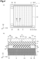
- thermoelectric conversion module according to a modification will be described with reference to FIGS. 4 and 5 .
- redundant descriptions overlapping with the above-described embodiment are omitted, and different parts are described. That is, within the technically possible range, the descriptions of the above-described embodiment may be appropriately used in the modification.
- thermoelectric conversion module 1A according to the first modification is different from the thermoelectric conversion module 1 of the above-described embodiment in that it includes thermal conduction parts 5A instead of the thermal conduction parts 5, and further includes a capacitor C3.
- Each thermal conduction part 5A is a portion exhibiting higher thermal conductivity than that of the substrate 2 and has a band shape in a plan view.
- the thermal conductivity of each thermal conduction part 5A is, for example, 3 W/mK or more and 400 W/mK or less. Accordingly, when the thermoelectric conversion module 1 is heated, heat is favorably transferred to the thermoelectric conversion part 11 via the plurality of thermal conduction parts 5A.
- the thermal conductivity may be 5 W/mK or more, 8 W/mK or more, or 10 W/mK or more.
- the length T4 of each thermal conduction part 5A along the thickness direction D1 is greater than the length T3 of the thermal insulating member 6 and is, for example, 50 ⁇ m or more and 2000 ⁇ m or less.
- Each thermal conduction part 5A includes, for example, metal (silver, copper, or the like.), carbon, resin (for example, silicone resin, epoxy-based resin, (meth)acrylic-based resin) and the like.
- Each thermal conduction part 5 may include a ceramic such as boron nitride, aluminum nitride or the like that exhibits high thermal conductivity.
- the thermal conduction part 5A may include the above resin.
- the thermal conduction part 5A may be formed using the resin or a solution containing the resin.
- the capacitor C3 is thermally exchangeable with the thermoelectric conversion part 11 via the substrate 2 and at least one of the plurality of thermal conduction parts 5A, and exhibits flexibility. Therefore, the capacitor C3 can also function as a thermal conduction part.
- the capacitor C3 is a sheet capacitor overlapping each thermal conduction part 5A and each thermal insulating member 6 in the thickness direction D1 and electrically connected to the thermoelectric conversion part 11.
- the capacitor C3 is in contact with each thermal conduction part 5A and spaced apart from the thermal insulating member 6. Therefore, a space is provided between the capacitor C3 and the thermal insulating member 6 in the thickness direction D1. In the first modification, the capacitor C3 is in close contact with the thermal conduction parts 5A.
- the length T5 of the capacitor C3 along the thickness direction D1 is, for example, 50 ⁇ m or more and 2000 ⁇ m or less. In a plan view, the capacitor C3 is located inside the edges of the substrate 2, but is not limited thereto.
- the thermal conductivity of the capacitor C3 in the thickness direction D1 is preferably 3 W/mK or more, 5 W/mK or more, or 10 W/mK or more. Accordingly, when the thermoelectric conversion module 1A is heated, heat is favorably transferred to the thermoelectric conversion part 11 via the capacitor C3 and each thermal conduction part 5A. In addition, a part of the thermoelectric conversion part 11 can be quickly dissipated via the capacitor C3 and each thermal conduction part 5A.
- the capacitor C3 includes a plurality of first internal electrodes 51 and second internal electrodes 52 stacked each other in the thickness direction D1, a dielectric 53, and a pair of external electrodes 54 and 55 electrically connected to the thermoelectric conversion part 11.
- the functions, materials and the like of the plurality of first internal electrodes 51 and the plurality of second internal electrodes 52 are the same as those of the first internal electrode 5a1 and the second internal electrode 5a2 included in the capacitor of the above-described embodiment.
- the functions, materials and the like of the dielectric 53 are also the same as those of the dielectric 5b included in the capacitor of the above-described embodiment.
- the dielectric 53 is composed of a heat-resistant resin in which particles of an inorganic solid are dispersed.
- the resin may be identical to at least a part of the resin included in the dielectric 53.
- the capacitor C3 can be favorably in close contact to the thermal conduction part 5A by integrating the resins.
- the functions, materials and the like of the external electrodes 54 and 55 are the same as those of the external electrodes 5c and 5d included in the capacitor of the above-described embodiment.
- the external electrode 54 is in contact with another some electrodes included in each first internal electrode 51 and electrically connected to the first portion 7a of the connection part 7.
- the external electrode 55 is in contact with each second internal electrode 52 and electrically connected to the second portion 7b of the connection part 7.
- the external electrode 54 may be electrically connected to the first portion 7a via solder, via a wire or the like, or may be directly connected to the first portion 7a.
- the external electrode 55 may be electrically connected to the second portion 7b via solder, via a wire or the like, or may be directly connected to the second portion 7b.
- each of the thermal conductivities of the first internal electrodes 51, the second internal electrodes 52, the dielectric 53, and the external electrodes 54 and 55 may be 3 W/mK or more.
- the thermal conductivity may be 5.0 W/mK or more, or 10.0 W/mK or more.
- thermoelectric conversion module 1A according to the first modification described above, the same operations and effects as those of the above-described embodiment can be achieved.
- the power storage capacity of the thermoelectric conversion module 1A can be increased.
- FIG. 5 is a cross-sectional view of a main part of a thermoelectric conversion module according to a second modification.
- the thermoelectric conversion module 1B according to the second modification includes the capacitor C3, which is a sheet capacitor shown in the first modification, in addition to the thermoelectric conversion module 1 of the above-described embodiment.
- the capacitor C3 overlaps the thermal insulating member 6, the first capacitor C1, and the second capacitor C2 in the thickness direction D1, is in contact with the first capacitor C1 and the second capacitor C2, and is spaced apart from the thermal insulating member 6.
- the capacitor C3 is electrically connected to the thermoelectric conversion part 11 in the same manner as in the first modification.
- the capacitor C3 is connected in parallel with the plurality of thermal conduction parts 5 including the first capacitor C1 and the second capacitor C2.
- thermoelectric conversion module 1B according to the second modification described above, the same operations and effects as those of the above-described embodiment can be achieved, and in addition, the power storage capacity of the thermoelectric conversion module 1B can be further increased compared to the first modification.
- thermoelectric conversion module and the manufacturing method thereof according to the present disclosure are not limited to the above-described embodiment and modifications, and various other modifications are possible.
- thermoelectric conversion element is exposed on the first main face, but the present disclosure is not limited thereto.
- the thermoelectric conversion element may be covered with a resinous sealing layer or the like.
- an insulator may be provided between two adjacent thermoelectric conversion groups. In this case, from the viewpoint of maintaining the internal temperature difference of the thermoelectric conversion part, the thermal conductivity of the insulator is preferably low.
- the thermal insulating member is formed by drying a thermal insulating material coating on the substrate, but is not limited thereto.
- the thermal insulating member formed in advance may be fixed on the substrate.
Landscapes
- Engineering & Computer Science (AREA)
- Power Engineering (AREA)
- Manufacturing & Machinery (AREA)
- Microelectronics & Electronic Packaging (AREA)
- Cooling Or The Like Of Semiconductors Or Solid State Devices (AREA)
Applications Claiming Priority (2)
| Application Number | Priority Date | Filing Date | Title |
|---|---|---|---|
| JP2022143637 | 2022-09-09 | ||
| PCT/JP2023/030750 WO2024053430A1 (ja) | 2022-09-09 | 2023-08-25 | 熱電変換モジュール |
Publications (1)
| Publication Number | Publication Date |
|---|---|
| EP4577027A1 true EP4577027A1 (en) | 2025-06-25 |
Family
ID=90191161
Family Applications (1)
| Application Number | Title | Priority Date | Filing Date |
|---|---|---|---|
| EP23862969.5A Withdrawn EP4577027A1 (en) | 2022-09-09 | 2023-08-25 | Thermoelectric conversion module |
Country Status (4)
| Country | Link |
|---|---|
| EP (1) | EP4577027A1 (https=) |
| JP (1) | JP7799074B2 (https=) |
| TW (1) | TW202502187A (https=) |
| WO (1) | WO2024053430A1 (https=) |
Families Citing this family (1)
| Publication number | Priority date | Publication date | Assignee | Title |
|---|---|---|---|---|
| CN120432453B (zh) * | 2025-07-07 | 2025-09-05 | 上海新微技术研发中心有限公司 | 一种集成电路芯片的无源散热器件的制备方法 |
Family Cites Families (6)
| Publication number | Priority date | Publication date | Assignee | Title |
|---|---|---|---|---|
| JP4530927B2 (ja) | 2005-07-08 | 2010-08-25 | 関西電力株式会社 | 高耐熱フィルムコンデンサ |
| JP4869846B2 (ja) * | 2006-09-19 | 2012-02-08 | 新日本製鐵株式会社 | 電力変換素子 |
| JP4895293B2 (ja) | 2007-01-26 | 2012-03-14 | 新日鐵化学株式会社 | フレキシブル熱電変換素子及びその製造方法 |
| JP2010016308A (ja) * | 2008-07-07 | 2010-01-21 | Sumitomo Heavy Ind Ltd | 蓄電装置及びその作製方法 |
| JP5564455B2 (ja) * | 2011-03-17 | 2014-07-30 | 富士フイルム株式会社 | 熱電発電装置及び携帯型電子機器 |
| WO2021025059A1 (ja) * | 2019-08-08 | 2021-02-11 | デンカ株式会社 | 熱電変換素子 |
-
2023
- 2023-08-25 EP EP23862969.5A patent/EP4577027A1/en not_active Withdrawn
- 2023-08-25 WO PCT/JP2023/030750 patent/WO2024053430A1/ja not_active Ceased
- 2023-08-25 JP JP2024545565A patent/JP7799074B2/ja active Active
- 2023-09-06 TW TW112133804A patent/TW202502187A/zh unknown
Also Published As
| Publication number | Publication date |
|---|---|
| JPWO2024053430A1 (https=) | 2024-03-14 |
| WO2024053430A1 (ja) | 2024-03-14 |
| TW202502187A (zh) | 2025-01-01 |
| JP7799074B2 (ja) | 2026-01-14 |
Similar Documents
| Publication | Publication Date | Title |
|---|---|---|
| US20250048931A1 (en) | Thermoelectric conversion module and manufacturing method therefor | |
| CN113994488B (zh) | 热利用发电模块及具备其的热发电装置 | |
| JP7374624B2 (ja) | 熱発電装置 | |
| US20180183360A1 (en) | Thermoelectric conversion module | |
| US20240431207A1 (en) | Composite, layer including the composite, and module including the layer | |
| EP4577027A1 (en) | Thermoelectric conversion module | |
| JP2024030453A (ja) | 熱利用発電モジュール | |
| JP2024030452A (ja) | 熱利用発電モジュール | |
| US10347811B2 (en) | Thermoelectric conversion module | |
| US10115882B2 (en) | Thermoelectric conversion element and thermoelectric conversion module | |
| CN114207852B (zh) | 热电转换元件 | |
| JP6659836B2 (ja) | 熱電変換モジュール | |
| JP7745762B2 (ja) | 熱電変換モジュール及びその製造方法 | |
| JP7829674B2 (ja) | 熱電変換モジュール及びその製造方法 | |
| WO2024177071A1 (ja) | 熱電変換モジュール及びその製造方法 | |
| KR102026838B1 (ko) | 적층형 열전 모듈 및 이의 제조방법 | |
| WO2024237146A1 (ja) | 熱電変換モジュール | |
| WO2024177070A1 (ja) | 熱電変換モジュール |
Legal Events
| Date | Code | Title | Description |
|---|---|---|---|
| STAA | Information on the status of an ep patent application or granted ep patent |
Free format text: STATUS: THE INTERNATIONAL PUBLICATION HAS BEEN MADE |
|
| PUAI | Public reference made under article 153(3) epc to a published international application that has entered the european phase |
Free format text: ORIGINAL CODE: 0009012 |
|
| STAA | Information on the status of an ep patent application or granted ep patent |
Free format text: STATUS: REQUEST FOR EXAMINATION WAS MADE |
|
| 17P | Request for examination filed |
Effective date: 20250320 |
|
| AK | Designated contracting states |
Kind code of ref document: A1 Designated state(s): AL AT BE BG CH CY CZ DE DK EE ES FI FR GB GR HR HU IE IS IT LI LT LU LV MC ME MK MT NL NO PL PT RO RS SE SI SK SM TR |
|
| STAA | Information on the status of an ep patent application or granted ep patent |
Free format text: STATUS: THE APPLICATION HAS BEEN WITHDRAWN |
|
| 18W | Application withdrawn |
Effective date: 20250821 |