EP4567906A1 - Rückbeleuchtungsplatte und herstellungsverfahren dafür sowie anzeigetafel - Google Patents
Rückbeleuchtungsplatte und herstellungsverfahren dafür sowie anzeigetafel Download PDFInfo
- Publication number
- EP4567906A1 EP4567906A1 EP22757811.9A EP22757811A EP4567906A1 EP 4567906 A1 EP4567906 A1 EP 4567906A1 EP 22757811 A EP22757811 A EP 22757811A EP 4567906 A1 EP4567906 A1 EP 4567906A1
- Authority
- EP
- European Patent Office
- Prior art keywords
- substrate
- layer
- reflective layer
- white oil
- disposed
- Prior art date
- Legal status (The legal status is an assumption and is not a legal conclusion. Google has not performed a legal analysis and makes no representation as to the accuracy of the status listed.)
- Pending
Links
Images


Classifications
-
- H—ELECTRICITY
- H10—SEMICONDUCTOR DEVICES; ELECTRIC SOLID-STATE DEVICES NOT OTHERWISE PROVIDED FOR
- H10H—INORGANIC LIGHT-EMITTING SEMICONDUCTOR DEVICES HAVING POTENTIAL BARRIERS
- H10H20/00—Individual inorganic light-emitting semiconductor devices having potential barriers, e.g. light-emitting diodes [LED]
- H10H20/80—Constructional details
- H10H20/85—Packages
- H10H20/855—Optical field-shaping means, e.g. lenses
- H10H20/856—Reflecting means
-
- G—PHYSICS
- G02—OPTICS
- G02F—OPTICAL DEVICES OR ARRANGEMENTS FOR THE CONTROL OF LIGHT BY MODIFICATION OF THE OPTICAL PROPERTIES OF THE MEDIA OF THE ELEMENTS INVOLVED THEREIN; NON-LINEAR OPTICS; FREQUENCY-CHANGING OF LIGHT; OPTICAL LOGIC ELEMENTS; OPTICAL ANALOGUE/DIGITAL CONVERTERS
- G02F1/00—Devices or arrangements for the control of the intensity, colour, phase, polarisation or direction of light arriving from an independent light source, e.g. switching, gating or modulating; Non-linear optics
- G02F1/01—Devices or arrangements for the control of the intensity, colour, phase, polarisation or direction of light arriving from an independent light source, e.g. switching, gating or modulating; Non-linear optics for the control of the intensity, phase, polarisation or colour
- G02F1/13—Devices or arrangements for the control of the intensity, colour, phase, polarisation or direction of light arriving from an independent light source, e.g. switching, gating or modulating; Non-linear optics for the control of the intensity, phase, polarisation or colour based on liquid crystals, e.g. single liquid crystal display cells
- G02F1/133—Constructional arrangements; Operation of liquid crystal cells; Circuit arrangements
- G02F1/1333—Constructional arrangements; Manufacturing methods
- G02F1/1335—Structural association of cells with optical devices, e.g. polarisers or reflectors
- G02F1/1336—Illuminating devices
- G02F1/133602—Direct backlight
- G02F1/133612—Electrical details
-
- G—PHYSICS
- G02—OPTICS
- G02F—OPTICAL DEVICES OR ARRANGEMENTS FOR THE CONTROL OF LIGHT BY MODIFICATION OF THE OPTICAL PROPERTIES OF THE MEDIA OF THE ELEMENTS INVOLVED THEREIN; NON-LINEAR OPTICS; FREQUENCY-CHANGING OF LIGHT; OPTICAL LOGIC ELEMENTS; OPTICAL ANALOGUE/DIGITAL CONVERTERS
- G02F1/00—Devices or arrangements for the control of the intensity, colour, phase, polarisation or direction of light arriving from an independent light source, e.g. switching, gating or modulating; Non-linear optics
- G02F1/01—Devices or arrangements for the control of the intensity, colour, phase, polarisation or direction of light arriving from an independent light source, e.g. switching, gating or modulating; Non-linear optics for the control of the intensity, phase, polarisation or colour
- G02F1/13—Devices or arrangements for the control of the intensity, colour, phase, polarisation or direction of light arriving from an independent light source, e.g. switching, gating or modulating; Non-linear optics for the control of the intensity, phase, polarisation or colour based on liquid crystals, e.g. single liquid crystal display cells
- G02F1/133—Constructional arrangements; Operation of liquid crystal cells; Circuit arrangements
- G02F1/1333—Constructional arrangements; Manufacturing methods
- G02F1/1335—Structural association of cells with optical devices, e.g. polarisers or reflectors
- G02F1/1336—Illuminating devices
- G02F1/133602—Direct backlight
- G02F1/133603—Direct backlight with LEDs
-
- G—PHYSICS
- G02—OPTICS
- G02F—OPTICAL DEVICES OR ARRANGEMENTS FOR THE CONTROL OF LIGHT BY MODIFICATION OF THE OPTICAL PROPERTIES OF THE MEDIA OF THE ELEMENTS INVOLVED THEREIN; NON-LINEAR OPTICS; FREQUENCY-CHANGING OF LIGHT; OPTICAL LOGIC ELEMENTS; OPTICAL ANALOGUE/DIGITAL CONVERTERS
- G02F1/00—Devices or arrangements for the control of the intensity, colour, phase, polarisation or direction of light arriving from an independent light source, e.g. switching, gating or modulating; Non-linear optics
- G02F1/01—Devices or arrangements for the control of the intensity, colour, phase, polarisation or direction of light arriving from an independent light source, e.g. switching, gating or modulating; Non-linear optics for the control of the intensity, phase, polarisation or colour
- G02F1/13—Devices or arrangements for the control of the intensity, colour, phase, polarisation or direction of light arriving from an independent light source, e.g. switching, gating or modulating; Non-linear optics for the control of the intensity, phase, polarisation or colour based on liquid crystals, e.g. single liquid crystal display cells
- G02F1/133—Constructional arrangements; Operation of liquid crystal cells; Circuit arrangements
- G02F1/1333—Constructional arrangements; Manufacturing methods
- G02F1/1335—Structural association of cells with optical devices, e.g. polarisers or reflectors
- G02F1/1336—Illuminating devices
- G02F1/133602—Direct backlight
- G02F1/133605—Direct backlight including specially adapted reflectors
-
- G—PHYSICS
- G02—OPTICS
- G02F—OPTICAL DEVICES OR ARRANGEMENTS FOR THE CONTROL OF LIGHT BY MODIFICATION OF THE OPTICAL PROPERTIES OF THE MEDIA OF THE ELEMENTS INVOLVED THEREIN; NON-LINEAR OPTICS; FREQUENCY-CHANGING OF LIGHT; OPTICAL LOGIC ELEMENTS; OPTICAL ANALOGUE/DIGITAL CONVERTERS
- G02F1/00—Devices or arrangements for the control of the intensity, colour, phase, polarisation or direction of light arriving from an independent light source, e.g. switching, gating or modulating; Non-linear optics
- G02F1/01—Devices or arrangements for the control of the intensity, colour, phase, polarisation or direction of light arriving from an independent light source, e.g. switching, gating or modulating; Non-linear optics for the control of the intensity, phase, polarisation or colour
- G02F1/13—Devices or arrangements for the control of the intensity, colour, phase, polarisation or direction of light arriving from an independent light source, e.g. switching, gating or modulating; Non-linear optics for the control of the intensity, phase, polarisation or colour based on liquid crystals, e.g. single liquid crystal display cells
- G02F1/133—Constructional arrangements; Operation of liquid crystal cells; Circuit arrangements
- G02F1/1333—Constructional arrangements; Manufacturing methods
- G02F1/1335—Structural association of cells with optical devices, e.g. polarisers or reflectors
- G02F1/1336—Illuminating devices
- G02F1/133602—Direct backlight
- G02F1/133606—Direct backlight including a specially adapted diffusing, scattering or light controlling members
-
- G—PHYSICS
- G02—OPTICS
- G02F—OPTICAL DEVICES OR ARRANGEMENTS FOR THE CONTROL OF LIGHT BY MODIFICATION OF THE OPTICAL PROPERTIES OF THE MEDIA OF THE ELEMENTS INVOLVED THEREIN; NON-LINEAR OPTICS; FREQUENCY-CHANGING OF LIGHT; OPTICAL LOGIC ELEMENTS; OPTICAL ANALOGUE/DIGITAL CONVERTERS
- G02F1/00—Devices or arrangements for the control of the intensity, colour, phase, polarisation or direction of light arriving from an independent light source, e.g. switching, gating or modulating; Non-linear optics
- G02F1/01—Devices or arrangements for the control of the intensity, colour, phase, polarisation or direction of light arriving from an independent light source, e.g. switching, gating or modulating; Non-linear optics for the control of the intensity, phase, polarisation or colour
- G02F1/13—Devices or arrangements for the control of the intensity, colour, phase, polarisation or direction of light arriving from an independent light source, e.g. switching, gating or modulating; Non-linear optics for the control of the intensity, phase, polarisation or colour based on liquid crystals, e.g. single liquid crystal display cells
- G02F1/133—Constructional arrangements; Operation of liquid crystal cells; Circuit arrangements
- G02F1/1333—Constructional arrangements; Manufacturing methods
- G02F1/1335—Structural association of cells with optical devices, e.g. polarisers or reflectors
- G02F1/1336—Illuminating devices
- G02F1/133602—Direct backlight
- G02F1/133608—Direct backlight including particular frames or supporting means
-
- H—ELECTRICITY
- H10—SEMICONDUCTOR DEVICES; ELECTRIC SOLID-STATE DEVICES NOT OTHERWISE PROVIDED FOR
- H10H—INORGANIC LIGHT-EMITTING SEMICONDUCTOR DEVICES HAVING POTENTIAL BARRIERS
- H10H20/00—Individual inorganic light-emitting semiconductor devices having potential barriers, e.g. light-emitting diodes [LED]
- H10H20/80—Constructional details
- H10H20/85—Packages
- H10H20/8506—Containers
-
- H—ELECTRICITY
- H10—SEMICONDUCTOR DEVICES; ELECTRIC SOLID-STATE DEVICES NOT OTHERWISE PROVIDED FOR
- H10W—GENERIC PACKAGES, INTERCONNECTIONS, CONNECTORS OR OTHER CONSTRUCTIONAL DETAILS OF DEVICES COVERED BY CLASS H10
- H10W90/00—Package configurations
Definitions
- the present application relates to a field of display technologies, especially to a backlight board, a manufacturing method, and a display panel.
- a number of lamp beads of the lamp board of a mini light emitting diode (Mini-LED) backlight product is enormous such that a lamp board has a high demand to windows making precision for a white resist soldering ink, and generally a photosensitive type white oil is used. Because a reflectivity of the photosensitive type white oil is in proportion to a film thickness of the white oil, the film thickness of the white oil is drastically large when the reflectivity is required to be high. An excessively large thickness of the white oil would lead to incomplete cure of a bottom portion of the white oil when the white oil is exposed such that the incompletely cured white oil is etched from a side to form a bottom-cut structure during a development process.
- a bottom-cut structure is a hollow structure and is fragile and separate when subjecting to an external force, it results in a poor product and a dark lamp phenomenon when separated and falling into a soldering pads region. Furthermore, after a white oil with an excessively large thickness undergoes a high temperature process, inconsistency between thermal expansion coefficients of the white oil and glass generates a stress to lead to a substrate warpage, the excessive warpage easily causes a broken product.
- the embodiment of the present application provides a backlight board, including a substrate, a reflective layer, a white oil layer, soldering pads, and lamp beads;
- the embodiment of the present application provides a backlight board manufacturing method, including steps as follows:
- the embodiment of the present application provides a display panel, including a main control board, a diffuser board, a diffuser plate, a driver circuit board, a vertical polarizer, a thin film transistor (TFT) glass board, a liquid crystal layer, a color filter, a horizontal polarizer, and a backlight board;
- a display panel including a main control board, a diffuser board, a diffuser plate, a driver circuit board, a vertical polarizer, a thin film transistor (TFT) glass board, a liquid crystal layer, a color filter, a horizontal polarizer, and a backlight board;
- TFT thin film transistor
- the backlight board provided by each of embodiments the present application uses the substrate to carry the reflective layer, the white oil layer, the soldering pads, and the lamp beads. Windows configured to accommodate soldering pads are defined in the white oil layer.
- the lamp beads are electrically connected to the soldering pads.
- the reflective layer is configured to reflect light emitted from the electrified lamp beads to achieve reflection light emitted from the lamp beads to the reflective, improvement of the reflectivity of the backlight board, and enhancement of the light usage rate of the backlight board.
- the reflectivity of the backlight board enhanced on the reflective layer can reduce a usage amount of the white oil layer and decrease a thickness of the white oil layer.
- the thinned white oil layer can be completely cured during the curing process to prevent an issue of a bottom-cut structure generated during the development process and causing the broken white oil layer. Furthermore, the thinned white oil layer can also prevent an issue of warpage due to a thermal expansion coefficient greatly different from that of the substrate.
- a display panel is configured to display images or videos.
- the display panel generally includes a main control board, a diffuser board, a diffuser plate, a driver circuit board, a vertical polarizer, a thin film transistor (TFT) glass board, a liquid crystal layer, a color filter, a horizontal polarizer, and a backlight board 1.
- TFT thin film transistor
- the main control board is a control center of the display panel, is configured to control cooperation work of devices in the display panel.
- main control board includes a controller and a processor.
- the diffuser board can evenly diffuse light emitted from the backlight board 1 to a thin sheet or a thin film of an entire plane.
- a substrate material of the diffuser board is polyethylene terephthalate (PET), PC polycarbonate (PC), or polymethyl methacrylate (PMMA, organic glass).
- PET polyethylene terephthalate
- PC PC polycarbonate
- PMMA polymethyl methacrylate
- the diffuser plate can remove uneven brightness or bright spots.
- the diffuser plate is a thin sheet forming a protruding micro lens set on a main surface of a transparent sheet underlay.
- the driver circuit board provides lamp beads on the backlight board 1 with stable voltage or current driver signals.
- a vertical polarizer and a horizontal polarizer can control a polarizing direction of light beams.
- a material of the polarizer is polyvinyl alcohol.
- a thin film transistor (TFT) glass board is used for pixels in the display panel.
- the liquid crystal layer includes liquid crystal molecules configured to change an arrangement direction under an electrical field effect.
- the color filter is a color filter presenting colors, and allow a wave band of a light-wave within a small range to pass, and reflect other wave band of the light-wave.
- the backlight board 1 is a device providing the display panel with a light source.
- the backlight board 1 is an important part in the display panel.
- a conventional backlight board 1 easily has issues of broken white oil layer 15 and warpage of the backlight board 1.
- the embodiment of the present application provides a the backlight board 1.
- the backlight board 1 includes a substrate 11, a reflective layer 13, a white oil layer 15, soldering pads 17, and the lamp beads.
- the substrate 11 is configured to carry the reflective layer 13, the white oil layer 15, the soldering pads 17, and the lamp beads.
- the substrate 11 can be a transparent substrate 11, and also can be an opaque substrate 11.
- the transparent substrate 11 can be the glass substrate 11.
- the opaque substrate 11 is a printed circuit board (PCB) substrate 11, a metal substrate 11(for example, aluminum), etc..
- the substrate 11 can be set according to actual demands and is not limited particularly here.
- a surface of the white oil layer 15 has an anti-soldering function.
- the white oil layer 15 also has a certain reflective light effect.
- the white oil layer 15 is formed by curing the white ink.
- the soldering pads 17 is a connector of a current transmission cable configured to connect the lamp beads.
- internals of the soldering pads 17 are metal wirings, and an outer layer thereof is enclosed with an anti-oxidation layer, and the anti-oxidation layer is conductive. The lamp beads light when electrified.
- windows are defined in the white oil layer 15. It can be understood that the windows can be defined through or defined in the white oil layer 15, the soldering pads are defined in the windows.
- the lamp beads are electrically connected to the soldering pads 17. In particular, connecting ends of the lamp beads can be soldered to the soldering pads 17.
- the reflective layer 13 is disposed on the substrate 11.
- the reflective layer 13 is disposed on a side of the white oil layer 15 near the substrate 11, is configured to reflect light emitted from the electrified lamp beads such that light emitted from the lamp beads irradiates the diffuser board as much as possible to improve a usage rate of a light source.
- Selection of materials for manufacturing the reflective layer 13 depends on reflection characteristics of the material.
- the reflective layer 13 is made of white oil
- the reflective layer 13 is made of white glue
- the reflective layer 13 is made of copper
- the reflective layer 13 is made of aluminum
- the reflective layer 13 is made of silver
- the material for manufacture is not limited here.
- used manufacturing processes are also different, for example, the reflective layer 13 can be manufactured by a process such as printing, gluing, sputtering, and embedding.
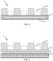
- the backlight board 1 includes the substrate 11, the reflective layer 13, the white oil layer 15, the soldering pads 17, and the lamp beads.
- the substrate 11 includes a first plate surface and a second plate surface opposite to each other. Namely, the first plate surface can be called a front surface of the substrate 11, and the front surface is disposed toward a diffuser board of the display panel.
- the second plate surface can be called a rear surface of the substrate 11, and the rear surface is disposed away from the diffuser board of the display panel.
- the white oil layer 15, the soldering pads 17, and the lamp beads are disposed on the first plate surface.
- the reflective layer 13 is disposed on the second plate surface.
- the white oil layer 15 is disposed on the first plate surface, windows are defined in the white oil layer 15, the soldering pads 17 are disposed in the windows, and the lamp beads are soldered to the soldering pads 17. A number of the windows is equal to that of the lamp beads. The nuber of the lamp beads is set according to actual demands.
- the substrate 11 is configured to carry the reflective layer 13, the white oil layer 15, the soldering pads 17, and the lamp beads. It should be explained that the white oil layer 15 in an aspect has an anti-soldering function. In another aspect, the white oil layer 15 also has a certain reflective light effect. In particular, the white oil layer 15 is formed by curing the white ink.
- the soldering pads 17 is a connector of a current transmission cable configured to connect the lamp beads.
- internals of the soldering pads 17 are metal wirings, and an outer layer thereof is enclosed with an anti-oxidation layer, and the anti-oxidation layer is conductive.
- the soldering pads 17 are metal soldering points.
- the lamp beads light when electrified.
- windows are defined in the white oil layer 15. It can be understood that the windows can be defined through or defined in the white oil layer 15, the soldering pads are defined in the windows.
- the lamp beads are electrically connected to the soldering pads 17. In particular, connecting ends of the lamp beads can be soldered to the soldering pads 17.
- the substrate 11 is a transparent substrate 11 to prevent light emitted from the lamp beads to extend through the substrate 11.
- light emitted from the electrified lamp beads extends through the substrate 11, is reflected by the reflective layer 13, extends back to the substrate 11, and then irradiates a diffuser board of the display panel.
- the reflective layer 13 aims at optical reflectivity, for example, the reflective layer 13 is made of white oil, the reflective layer 13 is made of white glue, the reflective layer 13 is made of copper, the reflective layer 13 is made of aluminum, or, the reflective layer 13 is made of silver.
- the material for manufacturing is not limited here.
- manufacturing processes are also different, for example, the reflective layer 13 can be manufactured by a process such as printing, gluing, and sputtering.
- An arrangement method of the reflective layer 13 in the example requires no change to the structure of the backlight board 1, but only needs to dispose a layer of the reflective layer 13 on a rear surface of the substrate 11 of the backlight board 1.
- the backlight board 1 further includes an auxiliary substrate 19.
- the auxiliary substrate 19 covers the reflective layer 13 such that the reflective layer 13 is sandwiched between the substrate 11 and the auxiliary substrate 19.
- the auxiliary substrate 19 can be made of a metal material, and also can be made of a non-metal material.
- the auxiliary substrate 19 is connected to the substrate 11 of the backlight board 1 by adhere or screws to further secure the reflective layer 13 and rely on a protective effect of the auxiliary substrate 19, which improves a usage lifespan of the reflective layer 13 to improve usage lifespans of the backlight board 1 and the display panel.
- the backlight board 1 includes the substrate 11, the reflective layer 13, the white oil layer 15, the soldering pads 17, and the lamp beads.
- the reflective layer 13 is embedded inside the substrate 11.
- the reflective layer 13 is manufactured in advance. During manufacturing the substrate 11 of the backlight board 1, the manufactured reflective layer 13 is immersed in a material for manufacturing the substrate 11. With cure of the material, the reflective layer 13 is embedded in the substrate 11 to form the substrate 11 with the reflective layer 13.
- the white oil layer 15 is disposed on the substrate 11, windows are defined in the white oil layer 15, the soldering pads 17 are disposed in the windows, and the lamp beads are soldered to the soldering pads 17.
- the white oil layer 15 has an anti-soldering function, and in another aspect the white oil layer 15 also has a certain reflective light effect.
- the white oil layer 15 is formed by curing the white ink.
- the soldering pads 17 are a connector of the current transmission cable configured to connect the lamp beads.
- the soldering pads 17 are copper metal soldering points.
- the lamp beads light when electrified.
- windows are defined in the white oil layer 15. It can be understood that the windows can be defined through or defined in the white oil layer 15, the soldering pads are defined in the windows.
- the lamp beads are electrically connected to the soldering pads 17. In particular, connecting ends of the lamp beads can be soldered to the soldering pads 17.
- the substrate 11 is a transparent substrate 11, for example, a plastic substrate 11 such that light emitted from the lamp beads is prevented from extending through the substrate 11.
- light emitted from the electrified lamp beads extends through the substrate 11, is reflected by the reflective layer 13, and irradiates a diffuser board of the display panel.
- a position of the reflective layer 13 embedded in the substrate 11 can be changed according to actual demands.
- the reflective layer 13 is embedded in a middle region of the substrate 11.
- embedding the reflective layer 13 in the substrate 11 can prevent the reflective layer 13 from oxidation and corrosion of air, water and improve reliability of the product.
- the backlight board 1 further includes the substrate 11, the reflective layer 13, the white oil layer 15, the soldering pads 17, the lamp beads, and a transparent insulation layer 21.
- the reflective layer 13 is disposed on an end surface of the substrate 11, the transparent insulation layer 21 is disposed on the reflective layer 13, and the white oil layer 15 is disposed on the transparent insulation layer 21.
- Windows are defined in the white oil layer 15, and the soldering pads 17 are disposed in the windows.
- the lamp beads are soldered to the soldering pads 17. It should be explained that the transparent insulation layer is configured to separate metal wirings corresponding to the reflective layer 13, the soldering pads 17, and the soldering pads 17.
- the reflective layer 13 When the reflective layer 13 is made of a conductive layer material, it prevents crosstalk between metal wirings of the soldering pads 17 and the reflective layer 13 and affecting electric power transmission from the metal wirings to the lamp beads, for example, the transparent insulation layer 21 is glass, plastic, etc..
- the white oil layer 15 in an aspect has an anti-soldering function, and in another aspect the white oil layer 15 also has a certain reflective light effect.
- the white oil layer 15 is formed by curing white ink.
- the soldering pads 17 are a connector of a current transmission cable configured to connect the lamp beads.
- the soldering pads 17 are silver metal soldering points. The lamp beads light when electrified.
- windows are defined in the white oil layer 15. It can be understood that the windows can be defined through or defined in the white oil layer 15, the soldering pads are defined in the windows.
- the lamp beads are electrically connected to the soldering pads 17. In particular, connecting ends of the lamp beads can be soldered to the soldering pads 17.
- the substrate 11 can be the transparent substrate 11, can also be the opaque substrate 11.
- light emitted from the electrified lamp beads extends through the transparent insulation layer 21, is reflected by the reflective layer 13, and extends back to the transparent insulation layer 21.
- the reflective layer 13 and other structures such as the white oil layer 15 are disposed in the same layer for convenience of setting processes.
- the reflective layer 13 can be a complete material layer. Namely, a continuous reflective layer 13 is formed on the substrate 11.
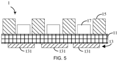
- the reflective layer 13 includes sub-reflective layers 131 having a number equal to that of the lamp beads.
- the reflective layer 13 is composed of a plurality of the sub-reflective layers 131, the sub-reflective layers 131 are independent from one another and have no contact with one another, namely, an emission layer is incomplete.
- the sub-reflective layers 131 on the substrate 11 are disposed to correspond to the lamp beads one by one, namely, each of the lamp beads is equipped with one of the sub-reflective layers 131.
- the sub-reflective layers 131 is configured to reflect light emitted from a corresponding one of the electrified lamp beads. According to the arrangement method of the reflective layer 13 on the substrate 11, similarly, the sub-reflective layers 131 can also have different formation methods.
- the reflective layer 13 is disposed on a second plate surface (a rear surface of the substrate 11) of the substrate 11, in an example, the entire reflective layer 13 is disposed on the second plate surface first, and then the reflective layer 13 is cut according to arrangement positions of the lamp beads to form the sub-reflective layers 131.
- the sub-reflective layers 131 is manufactured in advance, and the sub-reflective layers 131 are disposed on positions corresponding to the lamp beads.
- the sub-reflective layers 131 is manufactured in advance, and the sub-reflective layers 131 are arranged according to arrangement positions of the lamp beads.
- the arranged the sub-reflective layers 131 is immersed in the material of the substrate 11, and then is cured.
- the reflective layer 13 and the white oil layer 15 are disposed on the same side of the substrate 11, in an example, the entire reflective layer 13 is disposed on an end surface of the substrate 11 first, then the reflective layer 13 is cut according to the arrangement positions of the lamp beads to form the sub-reflective layers 131.
- the sub-reflective layers 131 are manufactured in advance, and the sub-reflective layers 131 are disposed to correspond to the positions of the lamp beads. It should be explained that areas of the sub-reflective layers 131 are required to fulfill most of light reflected toward the reflective layer 13.
- the backlight board 1 in each embodiment, the substrate 11 is used to carry the reflective layer 13, the white oil layer 15, the soldering pads 17, and the lamp beads.
- the windows configured to accommodate the soldering pads 17 are defined in the white oil layer 15.
- the lamp beads are electrically connected to the soldering pads 17.
- the reflective layer 13 is configured to reflect light emitted from the electrified lamp beads to achieves reflection of light emitted from the lamp beads to the reflective layer 13, improvement of a reflectivity of the backlight board 1, and enhancement of light usage rate a of the backlight board 1.
- the reflectivity of the backlight board 1 enhanced on the reflective layer 13 can reduce a usage amount of the white oil layer 15, reduce the thickness of the white oil layer 15, and the thinned white oil layer 15 can be completely cured during the curing process to prevent the issue of a bottom-cut structure generated during the development process and causing the broken white oil layer 15. Furthermore, the thinned white oil layer 15 can also prevent the issue of warpage due to a thermal expansion coefficient greatly different from that of the substrate 11.
- a manufacturing method for the backlight board 1, as shown in FIG. 6 including steps as follows:
- the reflective layer 13 includes a plurality of sub-reflective layers 131
- a complete reflective layer 13 can be formed on the substrate 11 and then the reflective layer 13 is cut out, or the sub-reflective layers 131 is manufactured in advance, and then the sub-reflective layers 131 is disposed in the substrate 11. It should be explained that the reflective layer 13 is configured to partially reflect light from the electrified lamp beads on the backlight board 1.
- a step S65 includes forming soldering pads 17 on the substrate 11.
- the soldering pads 17 are disposed on the metal wirings.
- internals of the soldering pads 17 are metal wirings, and an outer layer thereof is enclosed with an anti-oxidation layer, and the anti-oxidation layer is conductive.
- the soldering pads 17 are metal soldering points.
- a step S67 includes forming a white oil layer 15 on the substrate 11, wherein windows are defined in the white oil layer 15, and the soldering pads 17 are disposed in the windows.
- a white ink is coated on the substrate 11 to cover the soldering pads 17, the white ink is cured, and then white ink is processed by processes of exposure and development to form windows to expose the soldering pads 17.
- a step S69 includes soldering the lamp beads on the soldering pads 17.
- the method further includes a step between the step S and the step S as follows:
- the transparent insulation layer 21 is formed on the reflective layer 13.
- the white oil layer 15 is formed on the transparent insulation layer 21.
- the transparent insulation layer is configured to separate metal wirings corresponding to the reflective layer 13, the soldering pads 17, and the soldering pads 17.
- the reflective layer 13 is made of a conductive layer material, it prevents crosstalk between metal wirings of the soldering pads 17 and the reflective layer 13 and affecting electric power transmission from the metal wirings to the lamp beads, for example, the transparent insulation layer 21 is glass, plastic, etc..
- the backlight board 1 manufactured by the manufacturing method of the present application uses the reflective layer 13 to reflect light emitted from the electrified lamp beads to achieves reflection of light emitted from the lamp beads to the reflective layer 13, improvement of a reflectivity of the backlight board 1, and enhancement of light usage rate a of the backlight board 1.
- the reflectivity of the backlight board 1 enhanced on the reflective layer 13 can reduce a usage amount of the white oil layer 15, reduce the thickness of the white oil layer 15, and the thinned white oil layer 15 can be completely cured during the curing process to prevent the issue of a bottom-cut structure generated during the development process and causing the broken white oil layer 15.
- the thinned white oil layer 15 can also prevent the issue of warpage due to a thermal expansion coefficient greatly different from that of the substrate 11.
Landscapes
- Physics & Mathematics (AREA)
- Nonlinear Science (AREA)
- Mathematical Physics (AREA)
- Chemical & Material Sciences (AREA)
- Crystallography & Structural Chemistry (AREA)
- General Physics & Mathematics (AREA)
- Optics & Photonics (AREA)
- Planar Illumination Modules (AREA)
- Liquid Crystal (AREA)
- Led Device Packages (AREA)
- Devices For Indicating Variable Information By Combining Individual Elements (AREA)
Applications Claiming Priority (2)
| Application Number | Priority Date | Filing Date | Title |
|---|---|---|---|
| CN202210916195.9A CN115360284A (zh) | 2022-08-01 | 2022-08-01 | 背光板、制备方法以及显示面板 |
| PCT/CN2022/110822 WO2024026903A1 (zh) | 2022-08-01 | 2022-08-08 | 背光板、制备方法以及显示面板 |
Publications (1)
| Publication Number | Publication Date |
|---|---|
| EP4567906A1 true EP4567906A1 (de) | 2025-06-11 |
Family
ID=84031936
Family Applications (1)
| Application Number | Title | Priority Date | Filing Date |
|---|---|---|---|
| EP22757811.9A Pending EP4567906A1 (de) | 2022-08-01 | 2022-08-08 | Rückbeleuchtungsplatte und herstellungsverfahren dafür sowie anzeigetafel |
Country Status (5)
| Country | Link |
|---|---|
| US (1) | US12197079B2 (de) |
| EP (1) | EP4567906A1 (de) |
| JP (1) | JP7668821B2 (de) |
| CN (1) | CN115360284A (de) |
| WO (1) | WO2024026903A1 (de) |
Families Citing this family (1)
| Publication number | Priority date | Publication date | Assignee | Title |
|---|---|---|---|---|
| CN117525102A (zh) * | 2023-02-14 | 2024-02-06 | Tcl华星光电技术有限公司 | 一种显示面板及其制备方法 |
Family Cites Families (14)
| Publication number | Priority date | Publication date | Assignee | Title |
|---|---|---|---|---|
| JP2005234117A (ja) | 2004-02-18 | 2005-09-02 | Sharp Corp | カラー液晶表示パネルの製造方法 |
| JP2011205142A (ja) | 2011-07-12 | 2011-10-13 | Sony Corp | 表示装置 |
| CN110225651B (zh) * | 2019-06-19 | 2020-12-04 | 深圳市洲明科技股份有限公司 | 线路板及显示屏 |
| CN110398857A (zh) * | 2019-07-15 | 2019-11-01 | 青岛海信电器股份有限公司 | 微型发光二极管灯板、其制作方法、背光模组及显示装置 |
| CN112698522B (zh) * | 2019-10-23 | 2025-03-14 | 京东方科技集团股份有限公司 | 显示面板及显示装置 |
| CN120091683A (zh) * | 2020-02-17 | 2025-06-03 | 京东方科技集团股份有限公司 | 背板 |
| CN111505868A (zh) * | 2020-05-11 | 2020-08-07 | Tcl华星光电技术有限公司 | 背光模组和显示面板 |
| CN111524931A (zh) * | 2020-05-11 | 2020-08-11 | 京东方科技集团股份有限公司 | 一种Mini LED显示面板及其制备方法和显示装置 |
| US11221518B2 (en) * | 2020-05-20 | 2022-01-11 | Tcl China Star Optoelectronics Technology Co., Ltd. | Backlight module and display panel |
| CN112241088B (zh) * | 2020-10-15 | 2021-09-03 | Tcl华星光电技术有限公司 | 一种微型发光二极管灯板、背光模组及其制备方法 |
| CN113985652A (zh) | 2021-10-19 | 2022-01-28 | 惠州视维新技术有限公司 | 一种背光板、显示装置及背光板的制备工艺 |
| CN215954024U (zh) | 2021-10-29 | 2022-03-04 | 深圳市盛腾光电有限公司 | 具有背光超薄化节能lcd模组 |
| CN114203879A (zh) * | 2021-12-10 | 2022-03-18 | Tcl华星光电技术有限公司 | 背光模组及背光模组的制备方法 |
| CN114628568B (zh) * | 2022-03-11 | 2025-02-21 | 上海天马微电子有限公司 | 发光面板和显示装置 |
-
2022
- 2022-08-01 CN CN202210916195.9A patent/CN115360284A/zh active Pending
- 2022-08-08 US US17/907,987 patent/US12197079B2/en active Active
- 2022-08-08 JP JP2022572451A patent/JP7668821B2/ja active Active
- 2022-08-08 WO PCT/CN2022/110822 patent/WO2024026903A1/zh not_active Ceased
- 2022-08-08 EP EP22757811.9A patent/EP4567906A1/de active Pending
Also Published As
| Publication number | Publication date |
|---|---|
| CN115360284A (zh) | 2022-11-18 |
| WO2024026903A1 (zh) | 2024-02-08 |
| US20240264489A1 (en) | 2024-08-08 |
| JP2024536652A (ja) | 2024-10-08 |
| US12197079B2 (en) | 2025-01-14 |
| JP7668821B2 (ja) | 2025-04-25 |
Similar Documents
| Publication | Publication Date | Title |
|---|---|---|
| CN113777826B (zh) | 一种显示装置 | |
| US11562991B2 (en) | Backplane and manufacturing method thereof, backlight module, and display panel using micro light-emitting diodes | |
| CN211979375U (zh) | 一种显示装置 | |
| US8662730B2 (en) | Display apparatus and method of assembling the same | |
| CN214098031U (zh) | 一种显示装置 | |
| US9651731B2 (en) | Light guide plate, manufacturing method of the same and display device comprising the same | |
| US20060103776A1 (en) | Liquid crystal display device | |
| CN113126363A (zh) | 一种显示装置 | |
| KR101804080B1 (ko) | 내로우 베젤 액정 디스플레이의 팬아웃 영역 구조 | |
| JP2011090977A (ja) | バックライトユニットおよびそれを備えた表示装置 | |
| KR20090079415A (ko) | 표시 장치용 광원 모듈 및 이를 포함하는 표시 장치 | |
| KR20080001755A (ko) | 백라이트 어셈블리 및 이를 구비한 액정표시장치. | |
| CN113777825A (zh) | 一种显示装置 | |
| KR20150041324A (ko) | 도광판 및 이를 구비한 백라이트 어셈블리 | |
| CN113568220A (zh) | 一种显示装置 | |
| US20120075883A1 (en) | Edge-type led backlight moudle | |
| KR20070033137A (ko) | 광학판, 이의 제조 방법 및 이를 갖는 표시 장치 | |
| EP2333592A2 (de) | Rückbeleuchtungseinheit und Anzeigevorrichtung damit | |
| KR20170034653A (ko) | 디스플레이 장치 | |
| EP4567906A1 (de) | Rückbeleuchtungsplatte und herstellungsverfahren dafür sowie anzeigetafel | |
| CN102197256A (zh) | 照明装置、面光源装置、显示装置和电视接收装置 | |
| CN116339014A (zh) | 发光模组、背光模组及显示装置 | |
| CN113703223B (zh) | 一种背光模组及其制备方法、显示面板 | |
| KR101762791B1 (ko) | 발광소자 어레이 | |
| CN221465780U (zh) | 一种抗跌落造成led灯跌坏的背光结构 |
Legal Events
| Date | Code | Title | Description |
|---|---|---|---|
| STAA | Information on the status of an ep patent application or granted ep patent |
Free format text: STATUS: UNKNOWN |
|
| STAA | Information on the status of an ep patent application or granted ep patent |
Free format text: STATUS: THE INTERNATIONAL PUBLICATION HAS BEEN MADE |
|
| PUAI | Public reference made under article 153(3) epc to a published international application that has entered the european phase |
Free format text: ORIGINAL CODE: 0009012 |
|
| STAA | Information on the status of an ep patent application or granted ep patent |
Free format text: STATUS: REQUEST FOR EXAMINATION WAS MADE |
|
| 17P | Request for examination filed |
Effective date: 20220831 |
|
| AK | Designated contracting states |
Kind code of ref document: A1 Designated state(s): AL AT BE BG CH CY CZ DE DK EE ES FI FR GB GR HR HU IE IS IT LI LT LU LV MC MK MT NL NO PL PT RO RS SE SI SK SM TR |
|
| DAV | Request for validation of the european patent (deleted) | ||
| DAX | Request for extension of the european patent (deleted) |