EP4567485A2 - Deckel für optische verpackungen - Google Patents
Deckel für optische verpackungen Download PDFInfo
- Publication number
- EP4567485A2 EP4567485A2 EP24212579.7A EP24212579A EP4567485A2 EP 4567485 A2 EP4567485 A2 EP 4567485A2 EP 24212579 A EP24212579 A EP 24212579A EP 4567485 A2 EP4567485 A2 EP 4567485A2
- Authority
- EP
- European Patent Office
- Prior art keywords
- substrate
- lid
- package
- circuit
- optical
- Prior art date
- Legal status (The legal status is an assumption and is not a legal conclusion. Google has not performed a legal analysis and makes no representation as to the accuracy of the status listed.)
- Pending
Links
Images







Classifications
-
- G—PHYSICS
- G02—OPTICS
- G02B—OPTICAL ELEMENTS, SYSTEMS OR APPARATUS
- G02B6/00—Light guides; Structural details of arrangements comprising light guides and other optical elements, e.g. couplings
- G02B6/24—Coupling light guides
- G02B6/42—Coupling light guides with opto-electronic elements
- G02B6/4292—Coupling light guides with opto-electronic elements the light guide being disconnectable from the opto-electronic element, e.g. mutually self aligning arrangements
-
- G—PHYSICS
- G02—OPTICS
- G02B—OPTICAL ELEMENTS, SYSTEMS OR APPARATUS
- G02B6/00—Light guides; Structural details of arrangements comprising light guides and other optical elements, e.g. couplings
- G02B6/24—Coupling light guides
- G02B6/42—Coupling light guides with opto-electronic elements
- G02B6/4201—Packages, e.g. shape, construction, internal or external details
- G02B6/4256—Details of housings
- G02B6/426—Details of housings mounting, engaging or coupling of the package to a board, a frame or a panel
-
- G—PHYSICS
- G02—OPTICS
- G02B—OPTICAL ELEMENTS, SYSTEMS OR APPARATUS
- G02B6/00—Light guides; Structural details of arrangements comprising light guides and other optical elements, e.g. couplings
- G02B6/24—Coupling light guides
- G02B6/42—Coupling light guides with opto-electronic elements
- G02B6/4201—Packages, e.g. shape, construction, internal or external details
- G02B6/4219—Mechanical fixtures for holding or positioning the elements relative to each other in the couplings; Alignment methods for the elements, e.g. measuring or observing methods especially used therefor
- G02B6/4236—Fixing or mounting methods of the aligned elements
- G02B6/424—Mounting of the optical light guide
- G02B6/4242—Mounting of the optical light guide to the lid of the package
-
- G—PHYSICS
- G02—OPTICS
- G02B—OPTICAL ELEMENTS, SYSTEMS OR APPARATUS
- G02B6/00—Light guides; Structural details of arrangements comprising light guides and other optical elements, e.g. couplings
- G02B6/24—Coupling light guides
- G02B6/42—Coupling light guides with opto-electronic elements
- G02B6/4201—Packages, e.g. shape, construction, internal or external details
- G02B6/4274—Electrical aspects
- G02B6/428—Electrical aspects containing printed circuit boards [PCB]
-
- G—PHYSICS
- G02—OPTICS
- G02B—OPTICAL ELEMENTS, SYSTEMS OR APPARATUS
- G02B6/00—Light guides; Structural details of arrangements comprising light guides and other optical elements, e.g. couplings
- G02B6/24—Coupling light guides
- G02B6/42—Coupling light guides with opto-electronic elements
- G02B6/4201—Packages, e.g. shape, construction, internal or external details
- G02B6/4246—Bidirectionally operating package structures
-
- G—PHYSICS
- G02—OPTICS
- G02B—OPTICAL ELEMENTS, SYSTEMS OR APPARATUS
- G02B6/00—Light guides; Structural details of arrangements comprising light guides and other optical elements, e.g. couplings
- G02B6/24—Coupling light guides
- G02B6/42—Coupling light guides with opto-electronic elements
- G02B6/4201—Packages, e.g. shape, construction, internal or external details
- G02B6/4249—Packages, e.g. shape, construction, internal or external details comprising arrays of active devices and fibres
-
- G—PHYSICS
- G02—OPTICS
- G02B—OPTICAL ELEMENTS, SYSTEMS OR APPARATUS
- G02B6/00—Light guides; Structural details of arrangements comprising light guides and other optical elements, e.g. couplings
- G02B6/24—Coupling light guides
- G02B6/42—Coupling light guides with opto-electronic elements
- G02B6/4201—Packages, e.g. shape, construction, internal or external details
- G02B6/4251—Sealed packages
-
- H—ELECTRICITY
- H05—ELECTRIC TECHNIQUES NOT OTHERWISE PROVIDED FOR
- H05K—PRINTED CIRCUITS; CASINGS OR CONSTRUCTIONAL DETAILS OF ELECTRIC APPARATUS; MANUFACTURE OF ASSEMBLAGES OF ELECTRICAL COMPONENTS
- H05K1/00—Printed circuits
- H05K1/18—Printed circuits structurally associated with non-printed electric components
- H05K1/181—Printed circuits structurally associated with non-printed electric components associated with surface mounted components
-
- H—ELECTRICITY
- H05—ELECTRIC TECHNIQUES NOT OTHERWISE PROVIDED FOR
- H05K—PRINTED CIRCUITS; CASINGS OR CONSTRUCTIONAL DETAILS OF ELECTRIC APPARATUS; MANUFACTURE OF ASSEMBLAGES OF ELECTRICAL COMPONENTS
- H05K2201/00—Indexing scheme relating to printed circuits covered by H05K1/00
- H05K2201/10—Details of components or other objects attached to or integrated in a printed circuit board
- H05K2201/10007—Types of components
- H05K2201/10121—Optical component, e.g. opto-electronic component
Definitions
- the present disclosure relates, in general, to methods, systems, and apparatuses for implementing a semiconductor device comprising a lid for an optical package such as a co-packaged optics (CPO) package.
- a semiconductor device comprising a lid for an optical package such as a co-packaged optics (CPO) package.
- CPO co-packaged optics
- Co-Packaged Optics involves the integration of optics and electronics in a package aimed at addressing next generation bandwidth and power challenges. As data rates increase there is a strong trend to move high-speed signals of an optical transceiver closer to the switch silicon.
- a CPO package can include the mounting of optical transceivers proximate to the switch silicon.
- the CPO package may use a separate lid that is separate from the CPO package to couple the CPO package to the substrate.
- the purpose of the lid is to couple the CPO package to the substrate and to connect (e.g., electrically connect or the like) one or more connections of the CPO package to one or more connections of the substrate.
- an optical package comprises:
- the lid directly contacts at least one of the portion of the first circuit or the portion of the second circuit.
- the lid is configured to couple the optical package to a second substrate.
- the second substrate comprises a printed circuit board, and wherein the lid couples the optical package to the printed circuit board.
- the optical package further comprises a connector between the first substrate and the second substrate, wherein the lid comprises a fastener configured to couple the lid to the second substrate, wherein the fastener is configured to provide a force to form a first connection between the first substrate and the connector and a second connection between the connector and the second substrate.
- the lid comprises an opening configured to receive a source configured to transmit or receive the optical signal, wherein the source is coupled to the second circuit.
- the lid further comprises a cover configured to cover the opening.
- At least a portion of a bottom surface of the cover comprises a material configured to form a seal surrounding the source as the source enters the opening.
- the lid comprises an opening configured to receive a source configured to transmit or receive the optical signal, wherein the source is coupled to the second circuit, wherein the opening is formed by a sidewall of the lid, two walls extending from the sidewall, and a bar extending between the two walls extending from the sidewall, and wherein a first material is attached to a top surface of the bar.
- the lid further comprises a cover configured to cover the opening, and wherein a second material is attached to at least a portion of a bottom surface of the cover, and wherein the second material is configured to contact the first material and form a seal surrounding the source as the source enters the opening.
- the lid comprises an opening configured to receive a source configured to transmit or receive the optical signal, wherein the source is coupled to the second circuit, and wherein the lid further comprises a protrusion comprising a first end coupled to and extending from a sidewall of the lid into the opening and a second end coupled to the second circuit.
- a width of the protrusion is about a same width as a width of the second circuit.
- a bottom surface of the lid comprises a bar configured to distribute a force of the lid over the first substrate.
- the bar is located between two second circuits.
- a bottom surface of the lid comprises a slanted surface and wherein the slanted surface is positioned over at least one of the first circuit or the second circuit.
- an optical system comprises:
- the lid directly contacts the circuit.
- the second substrate comprises a printed circuit board.
- a lid for an optical package comprises:
- the lid is formed from at least one of copper, zinc, aluminum, or ceramic.
- Various embodiments provide tools and techniques for implementing semiconductor packages or chip packages including one or more lids or lid components for an optical package such as a CPO package are described herein.
- an optical package can include a first substrate; a first circuit coupled to the first substrate and configured to transmit or receive an electrical signal; a second circuit coupled to the first substrate and configured to transmit or receive an optical signal; and a lid configured to couple to the first substrate and configured to cover at least one of a portion of the first circuit or a portion of the second circuit.
- the lid can directly contact at least one of the portion of the first circuit or the portion of the second circuit and can be configured to couple the optical package to a second substrate.
- the second substrate can include a printed circuit board and the lid can couple the optical package to the printed circuit board.
- the optical package can further include a connector between the first substrate and the second substrate, the lid can include a fastener configured to couple the lid to the second substrate, and the fastener can be configured to provide a force to form a first connection between the first substrate and the connector and a second connection between the connector and the second substrate.
- the lid can include an opening configured to receive a source configured to transmit or receive the optical signal and the source can be coupled to the second circuit.
- the lid can further include a cover configured to cover the opening.
- at least a portion of a bottom surface of the cover can include a material configured to form a seal surrounding the source as the source enters the opening.
- the lid can include an opening configured to receive a source configured to transmit or receive the optical signal.
- the source can be coupled to the second circuit.
- the opening can be formed by a sidewall of the lid, two walls extending from the sidewall, and a bar extending between the two walls extending from the sidewall.
- a first material can be attached to a top surface of the bar.
- the lid can further include a cover configured to cover the opening and a second material can be attached to at least a portion of a bottom surface of the cover.
- the second material can be configured to contact the first material and form a seal surrounding the source as the source enters the opening.
- an optical system can include a first substrate, a second substrate, a connector between the first substrate and the second substrate configured to transmit a first signal between the first substrate and the second substrate, a circuit coupled to the first substrate and configured to at least one of transmit or receive an optical signal, and a lid configured to couple the first substrate to the second substrate and form a first connection between the first substrate and the connector and a second connection between the connector and the second substrate to transmit or receive the first signal between the first substrate and the second substrate.
- the lid can be further configured to directly cover at least a portion of the circuit.
- the lid can be configured to directly contact the circuit.
- the second substrate comprises a printed circuit board.
- a lid for an optical package can include a body comprising an opening configured to receive a source configured to transmit or receive an optical signal and a portion of a bottom surface of the body configured to directly cover at least a portion of a circuit coupled to the source and a first substrate.
- the lid can be configured to couple the first substrate to a second substrate and provide a force to form a first connection between the first substrate and a connector and a second connection between the connector and the second substrate to transmit or receive a first signal between the first substrate and the second substrate.
- the lid can be formed from at least one of copper, zinc, aluminum, or ceramic.
- a layer can be a single layer or include multiple layers.
- a conductive layer may comprise multiple different conductive materials or multiple layers of different conductive materials
- a dielectric layer may comprise multiple dielectric materials or multiple layers of dielectric materials.
- Circuits are composed of various electronic components such as resistors, capacitors, inductors, diodes, transistors, and integrated circuits. In some cases, integrated circuits can be formed from one or more circuits. These electronic components are carefully selected and interconnected to create a circuit that can perform a specific task or carry out a particular function. Circuits can be as simple as a basic switch that turns a light on and off, or they can be incredibly complex, such as those found in advanced computer systems, communication devices, or medical equipment. Circuits can be categorized into different types based on their purpose or function, including amplifiers, oscillators, filters, power supplies, and logic gates, among others. Additionally, circuits can include software or firmware in addition to hardware or instead of hardware to carry out a particular function.
- Photonic circuits can be composed of various electronic components such as resistors, capacitors, inductors, diodes, transistors, and integrated circuits and optical components such as lenses, optical sources, fibers, or the like. These electronic and optical components are carefully selected and interconnected to create a photonic circuit that can perform a specific task or carry out a particular function.
- photonic circuits can be configured to receive or transmit optical signals, convert electrical signals to optical signals or optical signals to electrical signals, or the like.
- photonic circuits can include software or firmware in addition to hardware or instead of hardware to carry out a particular function.
- circuits, modules, or other components may be described as “configured to” or “adapted to” perform a task or tasks.
- “configured to” or “adapted to” is a broad recitation of structure generally meaning “having circuitry that" performs the task or tasks during operation.
- the unit/circuit/module/component can be configured to perform the task even when the unit/circuit/module/component is not currently on.
- the circuitry that forms the structure corresponding to "configured to” or “adapted to” may include hardware circuits and/or memory storing program instructions executable to implement the operation.
- the memory can include volatile memory such as static or dynamic random-access memory and/or nonvolatile memory such as optical or magnetic disk storage, flash memory, programmable read-only memories, etc.
- volatile memory such as static or dynamic random-access memory
- nonvolatile memory such as optical or magnetic disk storage, flash memory, programmable read-only memories, etc.
- various unit/circuit/module/component may be described as performing a task or tasks, for convenience in the description. Such descriptions should be interpreted as including the phrase “configured to” or “adapted to.” Reciting a unit/circuit/component that is configured to perform one or more tasks is expressly intended not to invoke 35 U.S.C. ⁇ 112, paragraph six interpretation for that unit/circuit/component.
- left, right, front, back, top, bottom, forward, reverse, clockwise and counterclockwise are used for purposes of explanation only and are not limited to any fixed direction or orientation. Rather, they are used merely to indicate relative locations and/or directions between various parts of an object and/or components. Additionally, terms such as first, second, third, are merely used to distinguish elements or components from each other and are not intended to imply an order, sequence, or amount unless expressly stated otherwise.
- the phrase "at least one of” preceding a series of items, with the term “and” or “or” to separate any of the items, modifies the list as a whole, rather than each member of the list (i.e., each item).
- the phrase "at least one of” does not require selection of at least one of each item listed; rather, the phrase allows a meaning that includes at least one of any one of the items, and/or at least one of any combination of the items.
- the phrases “at least one of A, B, and C" or “at least one of A, B, or C” each refer to only A, only B, or only C; and/or any combination of A, B, and C. In instances where it is intended that a selection be of "at least one of each of A, B, and C," or alternatively, "at least one of A, at least one of B, and at least one of C,” it is expressly described as such.
- the CPO package is typically attached to one or more of a circuit board (e.g., a printed circuit board (PCB) or the like), a connector, a land grid array (LGA), another substrate, or the like by a lid that is separate from the CPO package or a housing of the CPO package.
- the lid is typically used to cover the CPO package comprising the housing including one or more dies (e.g., one or more electronic dies, one or more photonic dies, a combination of two or more dies, other dies, or the like) and attach the housing to one or more of the circuit board, the PCB, the connector, the LGA, another substrate, or the like.
- the lid typically makes poor thermal contact with an upper portion of the housing of the CPO package which can cause the one or more dies of the CPO package to overheat.
- the subject technology comprises a semiconductor device (e.g., chip, IC, PCB, substrate or other semiconductor device or module) that provides a lid configured to couple or attach an optical package, e.g., CPO package, to one or more of a circuit board, a PCB, a connector, an LGA, another substrate, or the like.
- the lid can be configured to directly cover or directly contact one or more dies of the CPO package without a housing between the lid and the one or more dies of the CPO package. By directly covering or directly contacting the one or more dies, heat can be more effectively dissipated from the CPO package. Further, other features of the lid will be discussed below that provide advantages over existing CPO packages that may use a separate lid.
- FIG. 1 is a perspective view of a first embodiment of a semiconductor device 100a comprising an optical package such as a CPO package 200. including a first substrate 202 having one or more components, in accordance with various embodiments.
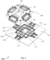
- FIG. 2 is an exploded view of the semiconductor device 100a comprising the CPO package 200 of FIG. 1 .
- FIG. 3 is a second embodiment of a semiconductor device 100b comprising a CPO package 200 including a first substrate (not shown) having one or more components, in accordance with various embodiments.
- the semiconductor device 100a and 100b are not intended to be limited to only the components shown in FIGS. 1-3 and could have more or less components than those shown.
- semiconductor device 100a could be included in semiconductor device 100b or components for semiconductor device 100b could be included in semiconductor device 100a or the like.
- semiconductor device 100a and semiconductor device 100b are referred to as semiconductor device 100.
- the semiconductor device 100 can include one or more of a second substrate 102 (e.g., a PCB, a circuit board, or the like) or a connector 104 or other semiconductor components, or the like.
- the CPO package 200 can be coupled to the second substrate 102 or connector 104.
- the CPO package 200 can be attached to the second substrate 102 or connector 104 via a lid 300 (e.g., lid 300a of FIGS. 1 and 2 or lid 300b of FIG. 3 ).
- the second substrate 102 can be a supporting material (e.g., silicon, silicon dioxide, aluminum oxide, gallium, germanium, ceramics, organic structures, laminated organic structures, and/or any other material or combination of materials) upon which or within which elements or components of the semiconductor device 100 or the CPO package 200 are fabricated or attached.
- the second substrate 102 can include one or more layers (not shown).
- the one or more layers can include, without limitation, one or more dielectric layers, one or more device or circuit layers, one or more conducting layers, one or more insulating layers, one or more redistribution layers, other layers, and/or the like.
- the layers may further include one or more routing layers or layers configured to provide component interconnections.
- the connector 104 (e.g., an LGA, an LGA socket, or the like) of the semiconductor device 100 can be configured to provide electrical interconnects 106 between the second substrate 102 and the CPO package 200.
- the connector 104 can have one or more electrical interconnects 106 (e.g., springs, pins, bumps, or the like) that provide the electrical connection between the second substrate 102 and the CPO package 200.
- electrical interconnects 106 e.g., springs, pins, bumps, or the like
- a first electrical connection can be formed between the connector 104 and the second substrate 102 and a second electrical connection can be formed between the connector 104 and the CPO package 200.
- the one or more electrical interconnects 106 can be arranged in an array or grid pattern or the like.
- the one or more electrical interconnects 106 can be formed from an electrically conductive material or combination of materials including, but not limited to, one or more of copper, aluminum, titanium, gold, silver, tin, nickel, lead, or a combination of metals/alloys, or may be formed of other electrically conductive material or ,combination of electrically conductive materials.
- the CPO package 200 can be configured to include a first substrate 202 (e.g., a package substrate, or the like).
- the first substrate 202 can be a supporting material (e.g., silicon, silicon dioxide, aluminum oxide, gallium, germanium, ceramics, organic structures, laminated organic structures, and/or any other material or combination of materials) upon which or within which elements or components of a semiconductor device 100 or the CPO package 200 are fabricated or attached.
- the first substrate 202 can include one or more layers (not shown).
- the one or more layers can include, without limitation, one or more dielectric layers, one or more device or circuit layers, one or more conducting layers, one or more insulating layers, one or more redistribution layers, other layers, and/or the like.
- the layers may further include one or more routing layers or layers configured to provide component interconnections. In a non-limiting example, connections may be routed, for example, from the second substrate 102 or connector 104 through the first substrate 202 to one or more circuits or dies coupled to the first substrate 202.
- the first substrate 202 is formed from one or more of silicon, silicon germanium, and/or other material or combination of materials.
- the first substrate 202 can include or be coupled to one or more circuits or dies.
- the one or more circuits or dies can include one or more electronic dies, first circuits, electronic circuits, or electronic integrated circuits (EICs) 204, one or more photonic dies, second circuits, photonic circuits, or photonic integrated circuits (PICs) 206, or the like as shown in FIG. 2 .
- EICs electronic integrated circuits
- PICs photonic integrated circuits
- the one or more electronic dies 204 can include one or more layers (not shown).
- the one or more layers can include, without limitation, one or more dielectric layers, one or more device or circuit layers, one or more conducting layers, one or more insulating layers, one or more redistribution layers, other layers, and/or the like.
- the layers may further include one or more layers configured to provide component interconnections. In a non-limiting example, connections may be routed, for example, through the electronic die 204 via one or more interconnects.
- the electronic die 204 is formed from one or more of silicon, silicon germanium, and/or other material or combination of materials.
- the one or more electronic dies 204 can include an electronic die 204a that can act as a processing unit (e.g., a central processing unit or the like) or a switch application specific integrated circuit (ASIC), or the like.
- the electronic die 204a can be configured to communicate with the one or more photonic dies 206 directly or through one or more controlling circuits or switch circuits 204b.
- the one or more electronic dies 204 can further include one or more controlling circuits or switch circuits 204b that are configured to communicate with electronic die 204a, photonic dies 206, or other circuits or dies not shown.
- the electronic die 204a and the one or more controlling circuits 204b of the electronic die 204 can be configured to control one or more operations of the one or more photonic dies 206, one or more devices in the one or more photonic dies 206, and/or other dies or devices (e.g., a switch die, a digital signal processor die, and/or other dies) disposed within CPO package 200 or semiconductor device 100.
- the one or more electronic dies 204 can also be configured to transmit electrical signals to or receive electrical signals from the one or more photonic dies 206 and/or other dies or devices disposed within semiconductor device 100.
- the one or more electronic dies 204 can include one or more circuits for processing one or more electrical signals that have been converted from one or more optical signals in the one or more photonic dies 206.
- the one or more electronic dies 204 can be coupled (e.g., communicatively coupled, electrically coupled, attached to, or the like) to one or more photonic dies or photonic integrated circuits (PICS) 206.
- the CPO package 200 can include eight photonic dies 206.
- the CPO package 200 should not be limited to only eight photonic dies, but could have more or less photonic dies.
- the one or more photonic dies can be formed from one or more of silicon, silicon nitride, indium phosphide, silicon on insulator (SOI), and/or the like.
- the one or more photonic dies 206 can include one or more layers (not shown).
- the one or more layers can include, without limitation, one or more dielectric layers, one or more device or circuit layers, one or more conducting layers, one or more insulating layers, one or more redistribution layers, other layers, and/or the like.
- the layers may further include one or more layers configured to provide component interconnections.
- connections may be routed, for example, through the one or more photonic dies 206 via one or more interconnects (not shown).
- the one or more interconnects of the one or more photonic dies 206 may be configured to provide one or more connections (e.g., electrical connections, optical connections, and/or the like).
- the one or more photonic dies 206 can be configured to be coupled (e.g., communicatively coupled, optically coupled, or the like) to one or more optical signal sources 208 such as optical fibers, optical wires, optical cables, photo diodes, light sources, laser dies, or the like.
- the one or more photonic dies 206 can have one or more circuits configured to receive, transmit, or convert one or more optical signals from the one or more optical signal sources 208.
- the one or more photonic dies 206 can be configured to receive one or more optical signals from the one or more optical signal sources, transmit the one or more optical signals inside the photonic die 206, transmit the one or more optical signals out of the one or more photonic dies 206, and/or the like.
- the one or more photonic dies 206 can be configured to convert the one or more optical signals received from the one or more optical signal sources 208 to one or more electrical signals and communicate the one or more electrical signals to the one or more electronic dies 204. In some cases, the one or more photonic dies 206 can be configured to receive one or more electrical signals from the one or more electronic dies 204 (e.g., to control the one or more optical sources, to transmit one or more optical signals, to convert one or more optical signals, or the like).
- the CPO package 200 can further include an optional housing 210 comprising walls 212.
- the housing 210 can be configured to surround an outer perimeter of the first substrate 202.
- the housing 210 can be part of the connector 104 configured to surround an outer perimeter of the first substrate 202.
- the CPO package 200 can further include a lid 300 configured to cover or couple to at least a portion of the CPO package (e.g., the first substrate 202, the one or more electronic dies 204, the one or more photonic dies 206, the optical sources 208, the housing 210, or the like).
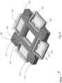
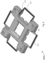
- FIGS. 1 , 2 , 5 -and 5-11 show a first embodiment of lid 300a and FIGS. 3 and 14 show a second embodiment of lid 300b.
- lid 300 When there are features that are common between lid 300a and 300b the lid will be referred to as lid 300.
- the lid 300 can have more or less components than those shown in FIGS.
- lid 300 should not be limited to only the components shown in FIGS. 1-14 .
- the components described with respect to FIGS. 1-14 could be arranged in a variety of configurations or arrangements and that the lid 300 should not be limited to the configuration and arrangements shown.
- components of lid 300a could be added to lid 300b, that components of lid 300b could be included in lid 300a, and that the lid 300 is not intended to be limited to only the embodiments shown in the figures.
- the lid 300 can be configured to couple to one or more of the second substrate 102, the connector 104, the first substrate 202, one or more electronic dies 204, one or more photonic dies 206, the housing 210, or the like. In various cases, the lid 300 can be configured to couple the CPO package 200 to one or more of the second substrate 102, the connector 104, or the like.
- the lid 300 can include a body 302 having an outer surface 304 and an inner surface 308.
- the lid 300 can further include one or more sidewalls 306.
- the lid 300 or body 302 might be sized and shaped to surround or cover an upper surface of the CPO package 200.
- the lid 300 is generally square or rectangular. However, other shapes of the lid 300 are possible.
- the lid 300 can be formed from a high strength, thermally conductive material or combination of materials including, but not limited to, at least one of copper, zinc, aluminum, or ceramic material or combination of materials or other high strength, thermally conductive material.
- the lid 300 can be formed using die-casting, forging, stamping, or metal injection molding, or the like
- the lid 300 can further include one or more fasteners 310 configured to couple to the outer surface 304 of the body 302.
- the fasteners 310 can be located at or near one or more corners 312 of the body 302 or around a perimeter 314 of the body 302.
- the fasteners 310 can include, without limitation, one or more screws, one or more bolts, glue, or other fastener configured to couple the body 302 of the lid 300 to one or more of the second substrate 102, the connector 104, the first substrate 202, one or more electronic dies 204, one or more photonic dies 206, the housing 210, or the like.
- fasteners 310 are shown and configured to couple the lid 300 to one or more of the second substrate 102, the connector 104, the first substrate 202, one or more electronic dies 204, one or more photonic dies 206, the housing 210, or the like.
- the one or more fasteners 310 can extend through one or more openings 316 of the body 302 and be configured to attach or directly attach to the second substrate 102 or the connector 104.
- the one or more fasteners 310 can be configured to apply a force to the CPO package 200 or to the first substrate 202 to couple the CPO package 200 or the first substrate 202 to the second substrate 102.
- the force applied by the fasteners 310 can further be configured to resist the force of the interconnects 106 of the connector 104 and form one or more connections between the interconnects 106 of the connector 104 and the second substrate 102 or the first substrate 202.
- each interconnect of the connector 104 may typically need between 10-30 grams of force to form an electrical connection between the interconnect 106 and the second substrate 102 or first substrate 202.
- the force needed to ensure an electrical connection between the interconnects 106 of the connector 104 and the second substrate 102 or first substrate 202 can be high because the lid 300 needs to be configured to resist the force of each interconnect 106 of the connector 104.
- the force can be distributed over the body 302 of the lid 300 forcing the first substrate 202 or CPO package 200 downward and forming an electrical connection between the one or more interconnects 106 of the connector 104 and the second substrate 102 or the first substrate 202.
- the body 302 of the lid 300 about 8 millimeters (mm) to about 12 mm thick, the force of the fasteners 310 can be more evenly distributed throughout the body 302 and the body 302 can be prevented from or experience limited warping.
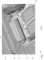
- the lid 300a can further include one or more optional openings 318 extending through a top surface 320 of the lid 300a.
- the one or more optical signal sources 208 can be configured to enter the CPO package 200 through the one or more openings 318 and couple to one or more photonic dies 206.
- the one or more openings 318 can be formed by a portion of the sidewall 306 of the lid 300a, two opening walls 322a and 322b extending from the sidewall 306, and a bar 324 (e.g., rod, crossbar, crosspiece, member, beam, or the like) extending between walls 322a and 322b.
- the walls 322a and 322b can be sloped or slanted (e.g., about 20 degrees to about 50 degrees or the like).
- the bar 324 extending across the walls 322a and 322b can be used to further support or provide rigidity to the lid 300a coupled to the first substrate 202, second substrate 102, or the like.
- lids 300a there are four openings 318 extending through the body 302 of the lid 300a. For example, there is one opening on each side of the lid 300a. In various embodiments, there could be more or less openings 318 depending on how many optical sources 208, photonic dies 206, or the like are needed for CPO package 200.
- the one or more openings 318 can be covered by one or more optional covers 326 as shown in FIGS. 1 , 2 , and 6 .
- the one or more covers 326 can be one or more environmental protectors configured to prevent dust, smoke, moisture, or other debris from entering the one or more openings 318.
- Environmental protection is important to protect the one or more optical signal sources 208 as just a small amount of dust, smoke, moisture, other debris, or the like can cause the loss of light and the improper functioning of the CPO package 200.
- the one or more covers 326 can be formed from a polycarbonate material or other material, or the like.
- At least one of a top surface 328 of the walls 322, a top surface 330 of the bar 324, or at least a portion one of a bottom surface 332 of the one or more covers 326 can be lined with a compliant (e.g., deformable, soft, flexible, or the like) material 334 as shown in FIGS. 1 , 6 , and 8 .
- the material 334 could be foam, fabric, rubber, silicone rubber material, or other soft material, flexible material, compliant material, or deformable material, or combination of materials, or the like.
- a width of the material 334 could be about a same width as a top surface 328 of the walls 322, a top surface 330 of the bar 324, or a bottom surface 332 of the one or more covers 326, or the like.
- the material 334 can have a tacky or sticky surface that allows the material 334 to be adhered to one or more of the top surface 328 of the walls 322, the top surface 330 of the bar 324, or at least the portion one of the bottom surface 332 of the covers 326.
- the material 334 could be place on the top surface 330 of a bar 324 and a bottom surface 332 of the cover 326 located over the bar 324 to form a seal (e.g., a full seal, a substantial seal, at least a partial seal, or the like) between the top surface 330 of the bar 324 and the bottom surface 332 of the cover 326 located over the bar 324.
- a seal e.g., a full seal, a substantial seal, at least a partial seal, or the like
- the seal can be formed by the material 334 on the top surface 330 of the bar 324 contacting the material 334 of the bottom surface 332 of the cover 326 and deforming around the optical signal sources 208 to enclose, fill, or block any gaps or openings between the top surface 330 of the bar 324, the bottom surface 332 of the cover 326, and the optical signal sources 208 thereby preventing (e.g., fully preventing, substantially preventing, at least partially preventing, or the like) or inhibiting (e.g., fully inhibiting, substantially inhibiting, at least partially inhibiting, or the like) material from passing between the top surface 330 of the bar 324 and the bottom surface 332 of the cover 326.
- preventing e.g., fully preventing, substantially preventing, at least partially preventing, or the like
- inhibiting e.g., fully inhibiting, substantially inhibiting, at least partially inhibiting, or the like
- the optical signal sources 208 can be prevented or inhibited from deforming or bending. Further, the material 334 on the top surface 330 of the bar 324 and the bottom surface 332 of the cover 326 can form the seal configured to prevent or inhibit dust, smoke, moisture, or the like from entering the one or more openings 318 and disrupting the light of the one or more optical sources 208.
- the one or more openings 318 might not be included in the lid 300b as shown in FIG. 3 .
- material 334 can still be included between a bottom surface 336 of the lid 300 and a top surface 338 of the first substrate 202 to form a seal (e.g., a full seal, a substantial seal, at least a partial seal, or the like) between the bottom surface 336 of the lid 300 and the top surface 338 of the first substrate 202.
- the seal can be formed by the material 334 on the bottom surface 336 of the lid 300 contacting the top surface 338 of the first substrate 202 and deforming to enclose, fill, or block any gaps or openings between the bottom surface 336 of the lid 300 and the top surface 338 of the first substrate 202 thereby preventing (e.g., fully preventing, substantially preventing, at least partially preventing, or the like) or inhibiting (e.g., fully inhibiting, substantially inhibiting, at least partially inhibiting, or the like) material from passing between the bottom surface 336 of the lid 300 and the top surface 338 of the first substrate 202.
- the material 334 can be placed on both the bottom surface 336 of the lid 300 and the top surface 338 of the first substrate 202.
- the material 334 can extend about an entire perimeter of the bottom surface 336 of the lid 300b or the top surface 338 of the first substrate 202.
- the material 334 can be placed at selected locations (e.g., at one or more locations where the optical signal sources 208 enter the CPO package 200, at locations of high stress of the lid 300b, or the like) on the bottom surface of the lid 300b or the top surface of the first substrate 202.
- the optical signal sources 208 can be prevented or inhibited from deforming or bending.
- the material 334 can prevent or inhibit dust, smoke, moisture, or the like from entering the CPO package 200 and disrupting the light of the one or more optical sources 208.
- the material 334 can further be placed between the bottom surface 336 of the lid 300 and the top surface 338 of the first substrate 202. This can be done in addition to or alternative to between each of the covers 326 and a corresponding bar 324. In some instances, the material 334 can extend about an entire perimeter of the bottom surface 336 of the lid or a top surface 338 of the first substrate 202.
- the material 334 can be placed at selected locations (e.g., at one or more locations where the optical signal sources 208 enter the CPO package 200, at locations of high stress of the lid 300, or the like) on the bottom surface 336 of the lid 300 or the top surface 338 of the first substrate 202.
- a seal e.g., a full seal, a substantial seal, at least a partial seal, or the like
- the seal can be formed by the material 334 on the bottom surface 336 of the lid 300 contacting the top surface 338 of the first substrate 202 and deforming to enclose, fill, or block any gaps or openings between the bottom surface 336 of the lid 300 and the top surface 338 of the first substrate 202 thereby preventing (e.g., fully preventing, substantially preventing, at least partially preventing, or the like) or inhibiting (e.g., fully inhibiting, substantially inhibiting, at least partially inhibiting, or the like) material from passing between the bottom surface 336 of the lid 300 and the top surface 338 of the first substrate 202.
- the seal can be configured to prevent dust, smoke, moisture, debris, or the like from entering the CPO package 200 and protecting one or more of the electronic dies 204, the photonic dies 206, and one or more other components of the CPO package 200.
- the lid 300 can further include one or more protrusions 340 extending from the one or more sidewalls 306 of the body 302 of the lid 300.
- the one or more protrusions 340 can extend into the one or more openings 318.
- the protrusions 340 can include a first end 342 configured to attach or directly attach to a corresponding sidewall 306 of the body 302 and a second end 344 configured to attach or directly attach to a corresponding photonic die 206 or electronic die 204.
- an optional epoxy, glue, or other attachment structure can be used to couple the second end 344 of the protrusion 340 to the photonic die 206 or electronic die 204.
- each protrusion 340 can correspond to a photonic die 206 or electronic die 204.
- a width of the protrusion can be about a same or substantially a same width as the width of the corresponding photonic die 206 or electronic die 204.
- the photonic die 206 or electronic die 204 can be well supported within the CPO package 200 and prevented or experience limited warping or deformation within the CPO package 200.
- protrusions 340 there could be more or less protrusions 340 than photonic dies 206 or electronic dies 204.
- two or more protrusions 340 could be coupled to a single photonic die 206 or electronic die 204 or one protrusion 340 can be configured to couple to two or more photonic dies 206 or electronic die 204.
- the lid 300 can further include one or more support bars 346 (e.g., beams, protrusions, raised elements, or the like) coupled to the bottom surface 332 of the lid 300.
- the one or more support bars 346 can further support or protect one or more of the one or more electronic dies 204 or the one or more photonic dies 206 or the like.
- a bottom surface of the support bars 346 can contact or directly contact the top surface 338 of the first substrate, an electronic die 204, or a photonic die 206.
- the one or more support bars 346 can be placed at selected locations on the bottom surface 332 of the lid.
- one or more support bars 346a can be placed between two photonic dies 206 or two electronic dies 204.
- one or more support bars 346b can be placed toward and around an inner aperture 348 of the lid 300.
- the bottom surface 332 of the lid 300 can contact (e.g., directly contact or indirectly contact) one or more of the one or more electronic dies 204 or one or more of the photonic dies 206.
- a thermal path can be created between the one or more electronic dies 204 or the one or more photonic dies 206 and the lid 300.
- heat is able to move upward from one or more of the one or more electronic dies 204 or the one or more photonic dies 206 through the lid 300 and dissipate away from one or more of the one or more electronic dies 204 or the one or more photonic dies 206.
- the first substrate, one or more electronic dies 204, or the one or more photonic dies 206 can further be prevented or inhibited from deforming because the force of the lid can be distributed over a larger area of the first substrate, one or more electronic dies 204, or the one or more photonic dies 206.
- the bottom surface 332 of the lid 300 contacting one or more of the one or more electronic dies 204 or one or more of the photonic dies 206 can be a slanted surface 350.
- the one or more slanted surfaces 350 can be located above one or more of the one or more electronic dies 204 or the one or more photonic dies 206. In some cases, the one or more slanted surfaces 350 can directly contact or indirectly contact one or more of the one or more electronic dies 204 or the one or more photonic dies 206.
- the slanted surfaces 350 can be configured to deflect radiation (indicated by lines 351) away from one or more sensitive areas (e.g., transmitters, receivers, or other sensitive areas or the like) of the one or more electronic dies 204 or the one or more photonic dies 206. In various cases, the slanted surfaces 350 can be sloped between about 1 degree to about 10 degrees.
- the lid 300 can also include one or more adhesive surfaces 352.
- the adhesive surface 352 can be configured to cover an entire bottom surface 332 of the lid 300 or be formed at selected locations (e.g., towards one or more corners 312 of the lid 300, at one or more locations where the lid 300 contacts the first substrate 202, or the like) of the bottom surface 332 of the lid.
- the adhesive surfaces 352 can be formed in a grid pattern or as one or more bumps or the like on the bottom surface 332 of the lid.
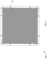
- the adhesive surfaces 352 are formed in a grid pattern towards one or more corners 312 of the bottom surface 332 of the lid 300.
- the adhesive surfaces 352 can be formed from a glue, epoxy, adhesive material, tacky material, or other material or combination of materials configured to adhere the lid 300 to the first substrate 202.
- the adhesive surfaces 352 can be configured to adhere the lid 300 to the first substrate 202 and increase the contact surface area between the lid 300 and the first substrate 202. By increasing the contact area between the lid 300 and the first substrate 202 heat can be more effectively dissipated from the first substrate 202.
- the lid 300 can further include an inner aperture 348 extending through the body 302 of the lid 300.
- the inner aperture 348 can be located towards a middle or center of the body 302.
- one or more aperture walls 354 of the aperture 348 can be tapered, sloped, slanted, chamfered, or filleted.
- the aperture 348 can be located above an electronic die 204a.
- the aperture 348 can be configured to receive a heat sink 400 or other cooling element such as a vapor chamber or the like as shown in FIG. 14 .
- the heat sink 400 or other cooling element can be configured to couple to the aperture 348 and directly contact the electronic die 204a to provide a thermal pathway to dissipate heat from the electronic die 206a.
- the lid 300 can include one or more additional openings 356, shown in FIG. 6 , to allow the heat sink 400 or other cooling element to be coupled to the top surface of the lid 300.
- one or more screws, bolts, or other attachment mechanisms can be coupled to openings 356 to couple the heat sink 400 or other cooling element to the lid 300.
- the lid 300 can further include one or more markers 358 (e.g., alignment markers, or the like) located on the top surface 338 of the lid 300.
- the one or more markers 358 can be used to determine how the lid 300 should be positioned on the first substrate 202.
- the one or more markers 358 can be aligned with one or more other markers on the first substrate 202 to ensure that the lid 300 is coupled to the first substrate 202 in a selected location or orientation.
- FIG. 15 is a flow diagram of a method of attaching a lid 300 to a semiconductor device 100, in accordance with various embodiments.
- the method described in FIG. 15 is one way the components of FIGS. 1-14 can be coupled. However, other methods may be used to couple the components of FIGS. 1-14 .
- the method 1500 may begin, at block 1505, by providing a first optical package (e.g., CPO package 200 or the like).
- a first optical package e.g., CPO package 200 or the like.
- the method can continue at optional block 1510 by providing a second substrate (e.g., second substrate 102, a circuit board, a PCB, another substrate, or the like) and at optional block 1515 by providing a connector (e.g., connector 104, an LGA, or the like).
- the method 1500, at block 1520, can further include coupling or attaching a lid (e.g., lid 300 or the like) to the optical package.
- a lid e.g., lid 300 or the like
- at least a portion of the lid can directly cover or directly contact one or more dies (e.g., electronic dies 204, photonic dies 206, other dies, or the like) of the optical package.
- the method 1500 can include coupling or attaching the lid to at least one of the second substrate or the connector.
- the lid can be used to couple or attach the optical package to at least one of the second substrate or the connector.
- the lid when the lid is used to couple or attach the optical package to the second substrate and the connector, the lid can provide a force that counters the force of the connector and forms a first electrical connection between the second substrate and the connector and a second electrical connection between the connector and the optical package.
Landscapes
- Physics & Mathematics (AREA)
- General Physics & Mathematics (AREA)
- Optics & Photonics (AREA)
- Optical Couplings Of Light Guides (AREA)
Applications Claiming Priority (2)
| Application Number | Priority Date | Filing Date | Title |
|---|---|---|---|
| US202363600172P | 2023-11-17 | 2023-11-17 | |
| US18/631,558 US20250164718A1 (en) | 2023-11-17 | 2024-04-10 | Lid for optical packages |
Publications (2)
| Publication Number | Publication Date |
|---|---|
| EP4567485A2 true EP4567485A2 (de) | 2025-06-11 |
| EP4567485A3 EP4567485A3 (de) | 2025-08-13 |
Family
ID=93521588
Family Applications (1)
| Application Number | Title | Priority Date | Filing Date |
|---|---|---|---|
| EP24212579.7A Pending EP4567485A3 (de) | 2023-11-17 | 2024-11-13 | Deckel für optische verpackungen |
Country Status (2)
| Country | Link |
|---|---|
| US (1) | US20250164718A1 (de) |
| EP (1) | EP4567485A3 (de) |
Family Cites Families (5)
| Publication number | Priority date | Publication date | Assignee | Title |
|---|---|---|---|---|
| DE19823691A1 (de) * | 1998-05-27 | 1999-12-02 | Siemens Ag | Gehäuseanordnung für Lasermodul |
| JP4812555B2 (ja) * | 2006-08-08 | 2011-11-09 | 富士通コンポーネント株式会社 | 光コネクタ |
| US10725254B2 (en) * | 2017-09-20 | 2020-07-28 | Aayuna Inc. | High density opto-electronic interconnection configuration utilizing passive alignment |
| US11432056B1 (en) * | 2019-07-26 | 2022-08-30 | Acacia Communications, Inc. | Switch |
| CN115421257B (zh) * | 2022-09-15 | 2024-10-01 | 青岛兴航光电技术有限公司 | 一种光模块 |
-
2024
- 2024-04-10 US US18/631,558 patent/US20250164718A1/en active Pending
- 2024-11-13 EP EP24212579.7A patent/EP4567485A3/de active Pending
Non-Patent Citations (1)
| Title |
|---|
| DAVID MEADOWCROFT ET AL., CPO INTEGRATED SOCKET LID IP REV A |
Also Published As
| Publication number | Publication date |
|---|---|
| US20250164718A1 (en) | 2025-05-22 |
| EP4567485A3 (de) | 2025-08-13 |
Similar Documents
| Publication | Publication Date | Title |
|---|---|---|
| JP5620330B2 (ja) | 並列光トランシーバ・モジュールと共に使用する、浮遊物体からこのモジュールの部品を保護するための保護ソケット | |
| US6958907B2 (en) | Optical data link | |
| US5761044A (en) | Semiconductor module for microprocessor | |
| US6040624A (en) | Semiconductor device package and method | |
| US6399418B1 (en) | Method for forming a reduced thickness packaged electronic device | |
| EP3151646B1 (de) | Anpassbare wärmebrücke | |
| US6586824B1 (en) | Reduced thickness packaged electronic device | |
| US9859186B2 (en) | Heat sink for a semiconductor chip device | |
| EP2234151A1 (de) | Halbleiterbauelement | |
| JP2003533009A (ja) | 2重格納部光電子パッケージ | |
| JP6880777B2 (ja) | 光モジュール | |
| US6894903B2 (en) | Optical data link | |
| KR20190066196A (ko) | 이미지 센서 모듈용 기판 구조체 및 이를 포함하는 이미지 센서 모듈 | |
| US6497518B1 (en) | Miniature opto-electronic transceiver | |
| KR20110126846A (ko) | 카메라 모듈 및 이의 제조 방법 | |
| CN103681617A (zh) | 半导体装置、通信设备以及半导体封装件 | |
| WO2020225578A1 (en) | Heat removal from silicon photonics chip using a recessed side-by-side thermal dissipation layout | |
| US12557411B2 (en) | Solid-state imaging device and electronic apparatus | |
| KR100626380B1 (ko) | 반도체 패키지 | |
| KR100696429B1 (ko) | 휴대형 기기에서의 카메라모듈의 배치 | |
| US7714422B2 (en) | Electronic module with a semiconductor chip and a component housing and methods for producing the same | |
| EP4567485A2 (de) | Deckel für optische verpackungen | |
| JP5349750B2 (ja) | レーザパッケージアダプタ | |
| KR20170082931A (ko) | 인쇄회로기판 및 이를 구비한 카메라 모듈 | |
| US6747820B2 (en) | Cooling opto-electronic packages |
Legal Events
| Date | Code | Title | Description |
|---|---|---|---|
| PUAI | Public reference made under article 153(3) epc to a published international application that has entered the european phase |
Free format text: ORIGINAL CODE: 0009012 |
|
| STAA | Information on the status of an ep patent application or granted ep patent |
Free format text: STATUS: THE APPLICATION HAS BEEN PUBLISHED |
|
| AK | Designated contracting states |
Kind code of ref document: A2 Designated state(s): AL AT BE BG CH CY CZ DE DK EE ES FI FR GB GR HR HU IE IS IT LI LT LU LV MC ME MK MT NL NO PL PT RO RS SE SI SK SM TR |
|
| PUAL | Search report despatched |
Free format text: ORIGINAL CODE: 0009013 |
|
| AK | Designated contracting states |
Kind code of ref document: A3 Designated state(s): AL AT BE BG CH CY CZ DE DK EE ES FI FR GB GR HR HU IE IS IT LI LT LU LV MC ME MK MT NL NO PL PT RO RS SE SI SK SM TR |
|
| RIC1 | Information provided on ipc code assigned before grant |
Ipc: G02B 6/42 20060101AFI20250707BHEP |
|
| STAA | Information on the status of an ep patent application or granted ep patent |
Free format text: STATUS: REQUEST FOR EXAMINATION WAS MADE |
|
| 17P | Request for examination filed |
Effective date: 20260203 |