EP4567477A1 - Optical element, optical system device, and optical system device manufacturing method - Google Patents
Optical element, optical system device, and optical system device manufacturing method Download PDFInfo
- Publication number
- EP4567477A1 EP4567477A1 EP23850169.6A EP23850169A EP4567477A1 EP 4567477 A1 EP4567477 A1 EP 4567477A1 EP 23850169 A EP23850169 A EP 23850169A EP 4567477 A1 EP4567477 A1 EP 4567477A1
- Authority
- EP
- European Patent Office
- Prior art keywords
- optical element
- medium layer
- concavo
- light
- convex shape
- Prior art date
- Legal status (The legal status is an assumption and is not a legal conclusion. Google has not performed a legal analysis and makes no representation as to the accuracy of the status listed.)
- Pending
Links
Images





Classifications
-
- G—PHYSICS
- G02—OPTICS
- G02B—OPTICAL ELEMENTS, SYSTEMS OR APPARATUS
- G02B27/00—Optical systems or apparatus not provided for by any of the groups G02B1/00 - G02B26/00, G02B30/00
- G02B27/09—Beam shaping, e.g. changing the cross-sectional area, not otherwise provided for
- G02B27/0927—Systems for changing the beam intensity distribution, e.g. Gaussian to top-hat
-
- G—PHYSICS
- G02—OPTICS
- G02B—OPTICAL ELEMENTS, SYSTEMS OR APPARATUS
- G02B27/00—Optical systems or apparatus not provided for by any of the groups G02B1/00 - G02B26/00, G02B30/00
- G02B27/09—Beam shaping, e.g. changing the cross-sectional area, not otherwise provided for
- G02B27/0938—Using specific optical elements
- G02B27/095—Refractive optical elements
- G02B27/0955—Lenses
- G02B27/0961—Lens arrays
-
- G—PHYSICS
- G02—OPTICS
- G02B—OPTICAL ELEMENTS, SYSTEMS OR APPARATUS
- G02B3/00—Simple or compound lenses
-
- G—PHYSICS
- G02—OPTICS
- G02B—OPTICAL ELEMENTS, SYSTEMS OR APPARATUS
- G02B3/00—Simple or compound lenses
- G02B3/0006—Arrays
- G02B3/0037—Arrays characterized by the distribution or form of lenses
- G02B3/0056—Arrays characterized by the distribution or form of lenses arranged along two different directions in a plane, e.g. honeycomb arrangement of lenses
Definitions
- the present disclosure relates to an optical element, an optical system device and a method for manufacturing the optical system device.
- Three-dimensional measurement sensors that utilize a Time Of Flight (TOF) scheme are now to be applied to portable devices, vehicles, and robots, etc. such a sensor measures a distance from an object based on a time until light emitted by a light source to an object is reflected and returns.
- TOF Time Of Flight
- the above-described sensor -based includes a light emitting unit that emits light, an optical element that controls the light from the light emitting unit into a predetermined light distribution, a camera unit that detects reflected light from each point of the object, and an arithmetic unit that calculates a distance from the object in accordance with a signal according to the light received by the camera unit.
- the light emitting unit the camera unit and the arithmetic unit, already-existing VCSEL, CMOS imager and CPU, etc., are applicable, respectively, and thus the unique component of the above-described -based is the light emitting unit.
- the TOF has needs for long-distance measurement, and emitted light needs an intensity that enables such a long-distance measurement.
- the microlens array having undergone the random placement has the high uniformity of emitted light but decreases the intensity thereof, it is not suitable for such a long-distance measurement.
- Patent Document 2 a scheme to utilize an optical element capable of emitting a dot pattern, and to execute a three-dimensional measurement from the Time Of Flight of such light is now examined (e.g., Patent Document 2).
- the present disclosure relates to an optical element that can be easily packaged with other structural components, an optical system device that utilizes such an optical element, and a method for manufacturing such an optical system device.
- an optical element according to the present disclosure includes:
- the first medium layer should be a gaseous body
- the second medium layer and the adjust portion should be integrally formed with each other by a second resin with the second refractive index.
- the second medium layer should be formed of a second resin with the second refractive index
- the first medium layer and the adjust portion should be integrally formed with each other by a first resin with the first refractive index.
- an opposite surface of the first medium layer or of the second medium layer to the boundary surface should be formed in a planar shape or in a curved shape.
- the optical element should further include an antireflection film formed on an opposite surface of the first medium layer or of the second medium layer to the boundary surface.
- an opposite surface of the first medium layer or of the second medium layer to the boundary surface should be provided with a fine concavo-convex structure that functions as a moth-eye.
- the optical element may further include a third medium layer formed on an opposite surface of the second medium layer to the boundary surface.
- the third medium layer may be formed of the same material as the first medium layer.
- the first medium layer should be formed on a base material.
- the optical element may further include greater than or equal to one functional layer which is formed on an opposite surface of the base material to a surface thereof where the first medium layer is present, and which has a particular function.
- the functional layer may be an aperture mask.
- the functional layer may be a metal wiring.
- the functional layer may include:
- the concavo-convex shape may be formed in a shape having a plurality of lenses arrayed at regular intervals.
- the diffusion range should be defined as an interior of a simple closed curve
- the concavo-convex shape should include a plurality of crests and valleys that have no regular interval
- the concavo-convex shape should be formed so as not to have a portion where a gradient of the concavo-convex shape changes by 135 degrees within a width range that is ⁇ /(n 2 -n 1 ) where ⁇ is a wavelength of the light, n 1 is the refractive index of the first medium layer, and n 2 is the refractive index of the second medium layer
- the concavo-convex shape should have a region that has a gradient causing incident light to be emitted to a region outside the diffusion range by Snell's law is smaller than or equal to 5 % of an entire region.
- the concavo-convex shape should be formed in such a way that a distributed light distribution calculated by Snell's law becomes proportional to cos -n ⁇ (where 1 ⁇ n ⁇ 7) from a center of the diffusion range toward a boundary thereof.
- An optical system device includes:
- the light emitting unit may include a light source covering layer which is formed of a resin and which covers the light source.
- the optical system device may further include a cover that encloses therein the optical element and the light emitting unit.
- the cover may be at least partially formed of a material with a light blocking effect.
- the concavo-convex shape should be formed in a shape in such a way that a plurality of lenses each allowing light with a wavelength ⁇ to pass therethrough is arrayed at regular intervals
- the light emitting unit should include the light source that emits the light with the wavelength ⁇ to the plurality of lenses, and a distance L 1 between the light emitting unit and a first focal plane of the lens, and a distance L 2 between the light emitting unit and a second focal plane should satisfy the following equations, respectively, where m and n are each a natural number that is greater than or equal to 1, f 1 is a focal point distance by a cross-sectional shape of the lens perpendicular to a y direction, f 2 is a focal point distance by a cross-sectional shape of the lens perpendicular to an x direction, P 1 is a dimension of a pitch of the lenses in the x direction, and P 2 is a dimension of a pitch in the y direction.
- a method for manufacturing an optical system device according to the present disclosure includes:
- Another method for manufacturing an optical system device according to the present disclosure includes:
- the optical element according to the present disclosure is provided with the adjust portion to maintain a certain distance from the concavo-convex shape of the optical element, packaging thereof with the light emitting unit and other structural components is facilitated.
- the optical element according to the present disclosure includes a concavo-convex shape 20 which accomplishes an optical function and which is placed at a boundary surface 11 between a first medium layer 1 with a first refractive index and a second medium layer 2 with a second refractive index that is higher than the first refractive index.
- the optical element according to the present disclosure is provided with an adjust portion 7 to maintain a certain distance from the concavo-convex shape 20 at the first-medium-layer-1 side relative to the concavo-convex shape 20 (the boundary surface 11).
- the term "certain distance” means a distance in the vertical direction and in the horizontal direction which should be maintained from the concavo-convex shape 20, a light emitting unit and other components at the time of assembling with the light emitting unit and the other components.
- the distance in the vertical direction should be maintained so as to exceed at least the heights of the convexities of the concavo-convex shape 20 at the first-medium-layer-1 side.
- the adjust portion 7 By forming the adjust portion 7, at the time of assembling with the light emitting unit and the other components, since alignment, etc., in the vertical direction and in the horizontal direction can be easily and precisely made, packaging when an optical system device is manufactured is facilitated. It is preferable that the adjust portion 7 should be integrally formed with the first medium layer 1 or with the second medium layer 2.
- the difference between the first refractive index and the second refractive index is not limited to any particular degree as far as at least the concavo-convex shape 20 can accomplish an optical function.
- it is preferable to increase the refractive index difference between the first refractive index and the second refractive index and for example, such a difference should be greater than or equal to 1.8, preferably, greater than or equal to 1.9, and more preferably, greater than or equal to 2.0.
- the first medium layer 1 should be a gaseous body.
- the gaseous body is not limited to any particular gas, but for example, air or an inert gas, etc., is applicable. Moreover, such a gaseous body includes a gas in a depressurized state that is called a vacuum state.
- a material through which at least light with a predetermined wavelength ⁇ can pass may be applied, and for example, resins (will be referred to as a second resin below), such as a silicon-based resin and an epoxy-based resin, and an acrylic resin, are applicable.
- the adjust portion 7 is formed as a lower portion of a lateral member 25 on the circumferential edge of the second medium layer 2 so as to maintain a certain distance from the concavo-convex shape 20, and to decide the thickness of the first medium layer 1 (the thickness of a space).
- the lateral member 25 may be formed of any materials.
- the second medium layer and the adjust portion 7 may be integrally formed with each other from a singular material (e.g., the second resin) that has the second refractive index.
- Such an optical element may be produced by any schemes, but for example, imprinting is applicable for production. More specifically, as for such a production, using a mold that has the inverted patterns of the concavo-convex shape 20 and of the adjust portion 7, the concavo-convex shape 20 may be formed on the material of the second medium layer. In this case, the concavo-convex shapes 20 and the adjust portions 7 may be formed across multiple regions, and then such multiple regions may be divided so as to produce a plurality of the optical elements.
- the optical element it is desirable in some cases to cause outgoing light from the lens to be narrow-angle.
- the sag of the lens may be reduced.
- the refractive index difference between the first refractive index and the second refractive index may be reduced. This enables, when for example, the concavo-convex shape 20 is a lenticular shape, a reduction of the outgoing angle of the lens with the dimension of the sag being maintained as it is.
- Such a refractive index difference may be smaller than or equal to 0.4, preferably, smaller than or equal to 0.2. This enables the outgoing angle of the lens to be smaller than or equal to 30 degrees with the sag thereof being maintained in a size that is greater than or equal to 10 ⁇ m.
- first medium layer 1 and the second medium layer 2 materials that have the small refractive index difference from each other may be selected.
- the materials of the first medium layer 1 and of the second medium layer 2 are not limited to any particular materials as far as light with at least a predetermined wavelength ⁇ can pass, but for example, a silicon-based resin, an epoxy-based resin, and an acrylic resin, etc., are applicable.
- an opposite surface 12 of the first medium layer 1 to the boundary surface 11 can be directly utilized as it is. That is, the thickness of the first medium layer 1 may be in a size that maintains a certain distance from the concavo-convex shape 20 at the first-medium-layer-1 side relative to the concavo-convex shape 20.
- Such an optical element may be produced in any schemes, but for example, imprinting may be applied for production. More specifically, as for such a production, using a mold that has the inverted patterns of the concavo-convex shape 20 and of the adjust portion 7, after the concavo-convex shape 20 is formed on the material of the first medium layer, the material of the second medium layer may be applied, or after the concavo-convex shape 20 is formed on the material of the second medium layer, the material of the first medium layer may be applied. At this time, the concavo-convex shape 20 may be formed with a large area or in multiple regions, and then may be divided so as to produce a plurality of the optical elements.
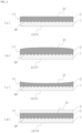
- an opposite surface 21 of the second medium layer 2 to the boundary surface 11 may be formed in a planar shape as illustrated in part (a) of FIG. 1 or in part (a) of FIG. 2 .
- the surface 21 can be formed in a curved shape as illustrated in parts (b) and (c) of FIG. 1 or in parts (b) and (c) of FIG. 2 .
- the term "planer shape” or "curved shape” means that there is no concavity and convexity which is larger than the wavelength of outgoing light, and such a shape is smooth enough. Adopting the planar shape or the curved shape facilitates addition of, to the surface 21, layers, films and shapes that have various functions.
- an antireflection film may be formed on the surface 21. This suppresses a reflection when light outgoes from the second medium layer 2.
- a fine concavo-convex structure that functions as a moth-eye may be formed on the surface 21. Such a fine concavo-convex structure may be formed so as to be smaller than the wavelength of passing light.
- the surface 21 may be provided with a third medium layer 3.
- the resin with a high refractive index often has low environmental characteristics. Accordingly, when the third medium layer 3 that eases the stress to the second medium layer 2 is placed on the surface of the second medium layer 2, the environmental characteristics of the optical element can be improved.
- the material of the third medium layer 3 is not limited to any particular materials as far as it can improve the environmental characteristics of the first medium layer 1 or of the second medium layer 2, but for example, a silicon-based resin, an epoxy-based resin, and an acrylic resin, etc., are applicable.
- the third medium layer 3 is formed of the same material as that of the first medium layer 1.
- the first medium layer 1 may be formed on a base material 5.
- This enables formation of greater than or equal to one functional layer 6 that has a particular function on an opposite surface 52 of the base material 5 to a surface 51 where the first medium layer 1 is present.
- the lower surface of the functional layer 6 can serve as the adjust portion 7.
- An example base material 5 is a glass substrate.
- an intermediate resin layer 4A may be formed on the surface 51 of the base material 5.
- An example intermediate resin layer 4A is a resin layer as an underlying layer that improves the intimate contact between the base material 5 and the second medium layer 2.
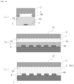
- the description that the first medium layer 1 is formed on the base material 5 means, as illustrated in parts (a) to (c) of FIG. 3 , not only a case in which the first medium layer 1 is directly in contact with the surface 51 of the base material 5, but also a case in which greater than or equal to one intermediate layer 4B is present on the base material 5 as illustrated in part (d) of FIG. 3 .
- An example intermediate resin layer 4B is a resin layer as an underlying layer that improves the intimate contact between the base material 5 and the first medium layer 1.
- the functional layer 6 is not limited to any particular layers as far as it has a particular function, but an example is, as illustrated in part (a) of FIG. 4 , an aperture mask 61.
- the aperture mask 61 is provided with an opening 61a, and blocks some of lights. This prevents electromagnetic waves that become noises from being emitted except through the opening 61a.
- An example aperture mask 61 is a metal like gold.
- another example functional layer 6 is a metal wiring 62 as illustrated in part (b) of FIG. 4 .
- the metal wirings 62 form a predetermined electric circuit, etc.
- the metal wirings 62 are formed on a lower surface 52 of the base material 5, and the concavo-convex shape 20 like lenses are formed on the resin layer 2A on the surface of such wirings.
- the metal wirings 62 are electrically insulated by the resin layer 2A, in order to accomplish an electrical conduction to the package side, it is necessary to further form a structure for such an electrical conduction.
- the concavo-convex shape 20 like lenses is formed on one-surface-51 side of the base material 5, and the metal wirings 62 are formed on the other-surface-52 side, the respective metal terminals of the metal wirings 62 can be exposed to the exterior. Hence, a structure for an electrical conduction to the package side like the light emitting unit 8 is unnecessary, and direct connection to the contacts at the package side can be accomplished.
- An example metal wiring 62 is ITO.
- the functional layer 6 may be a combination of layers each having a particular function.
- the functional layer is formed so as to include the metal wiring 62 like ITO formed on the surface 52 of the base material 5, an insulation layer 63 formed on the metal wiring 62, the aperture mask 61 formed of a metal formed on the insulation layer 63, and an electrical conduction portion 64 that electrically connects the metal wiring 62 to the aperture mask 61.
- This gives functions, such as eye-safe and EMI compatible functions, to the optical element.
- a connection between the contact at the package side and the metal wiring 62 can be easily accomplished.
- the concavo-convex shape 20 of the optical element is not limited to any particular ones as far as it has an optical function.
- a shape which controls incident light and which allows the controlled light to go out such as a microlens array (MLA) or a diffractive optical element (DOE), is an example.
- MLA microlens array
- DOE diffractive optical element
- the lenses of the microlens array may be arranged at regular intervals, or may be arranged at random.
- the optical element 100 capable of diffusing incident light to a predetermined diffusion range 91 as illustrated in FIG. 7 will be described.
- the diffusion range 91 of the optical element 100 is defined as the interior of a simple closed curve within a predetermined plane.
- the concavo-convex shape 20 includes a plurality of crests and of valleys that have no regular interval.
- the diffusion range 91 is defined as the interior of a simple closed curve 92, such as a polygon or an ellipse, within a predetermined plane 90.
- the predetermined plane 90 in this example means a plane (an xy plane) which is perpendicular to the optical axis (a z-axis) of a light source which emits light to the optical element, and which is apart from the optical element by at least greater than or equal to 100 times of the light size when emitted from a light source 2.
- the concavo-convex shape 20 is formed so as to cause incident light to be refracted within the diffusion range 91 by Snell's law. This will be described with reference to FIG. 9 .
- Snell's law is satisfied in a relation between an incidence angle ⁇ 3 to the emitting surface 21 of the optical element and a refraction angle ⁇ 4 of emitted light to the exterior.
- n 1 sin ⁇ 1 n 2 sin ⁇ 2
- the distributed light distribution of the emitted light i.e., the intensity distribution of the light emitting angle ⁇ 4 becomes a one-for-one relation to the frequency distribution of the incidence angle ⁇ 1 .
- the incidence angle ⁇ 1 is the same angle as an inclination angle (a gradient) ⁇ 1 of the rough surface (the surface of the concavo-convex shape 20) of the optical element, the frequency distribution of the incidence angle ⁇ 1 corresponds to the frequency distribution of the inclination angle ⁇ 1 of the rough surface of the optical element.
- y yo and ⁇ z/ ⁇ y
- y yo ))).
- x xo ))).
- the concavo-convex shape 20 in order to accomplish a predetermined distributed light intensity distribution, it is appropriate to calculate the frequency distribution of the inclination angle (a gradient) ⁇ 1 at the optical element surface to design the concavo-convex shape 20.
- the concavo-convex shape 20 should be designed in such a way that a region that has a gradient causing incident light to be emitted to a region outside the diffusion range 91 is smaller than or equal to 5 % of the entire region, preferably, smaller than or equal to 3 %, more preferably, smaller than or equal to 1 %.
- the concavo-convex shape 20 should have a height that is at least greater than or equal to 2.5 times of ⁇ /(n 2 -n 1 ), preferably, greater than or equal to 5 times, and more preferably, greater than or equal to 10 times where ⁇ is the wavelength of incident light to the optical element in a vacuum state, n 1 is the refractive index of the first medium layer 1, and n 2 is the refractive index of the second medium layer 2.
- ⁇ is the wavelength of incident light to the optical element in a vacuum state
- n 1 is the refractive index of the first medium layer 1
- n 2 is the refractive index of the second medium layer 2.
- the term "height of concavo-convex shape 20" means the difference between the highest crest of the concavo-convex shape 20 and the lowest valley thereof.
- the concavo-convex shape 20 when the surface of the concavo-convex shape 20 has a portion where the inclination angle ⁇ 1 (the gradient) keenly changes, this is not preferable because of adverse effects of scattering and of diffraction, etc. Hence, it is preferable that the inclination angle ⁇ 1 of the concavo-convex shape 20 should change gradually. More specifically, the concavo-convex shape 20 is formed in such a way that the surface thereof does not have a portion where the inclination angle ⁇ 1 (the gradient) changes by 135 degrees, preferably, by 120 degrees, and more preferably, by 90 degrees. Note that the change in inclination angle ⁇ 1 is ignorable as far as such a change is small and thus it cannot be sensed in light.
- the inclination angle ⁇ 1 at the surface of the concavo-convex shape 20 is calculated from a change in height within a width range that is ⁇ /(n 2 -n 1 ) from an arbitrary position to another arbitrary position where ⁇ is the wavelength of incident light to the optical element in a vacuum state, n 1 is the refractive index of the first medium layer 1, and n 2 is the refractive index of the second medium layer 2.
- the term "width" means the width of the concavo-convex shape 20 in a vertical direction to the z-axis direction (a parallel direction to the incidence surface or the emitting surface).
- a general sensor system mainly includes an optical element 100, a light emitting unit 8, a camera unit 300 that detects reflected light from each point on an object 10, and an arithmetic unit 400 that calculates a distance to the object in accordance with a signal based on the light received by the camera unit 300.
- the reflection angle the wider light is reflected and enters the camera unit 300, the lower the light intensity becomes.
- the larger an angle ⁇ of the light distribution of light passing through the optical element 100 is, the higher the light intensity becomes, which is preferable.
- the concavo-convex shape 20 should be formed in such a way that the distributed light distribution calculated by Snell's law monotonically increases from the center of a diffusion range 91 toward the boundary.
- the concavo-convex shape 20 of the optical element is designed in such a way that the frequency distribution of the inclination monotonically increases as the inclination increases.
- center of diffusion range 91 means a position of an intersection between the optical axis of the light source 2 and the diffusion range 91 when light from the light source 2 is perpendicularly emitted to the optical element of the present disclosure.
- boundary of diffusion range 91 means a part corresponding to the above-described closed curve 92 and a position of the maximum peak in the distributed light intensity distribution in the cross section.
- FIG. 11 is a graph in which the intensity of returning light to the camera unit is calculated relative to the incidence angle ⁇ when the light intensity distribution P( ⁇ ) at a far field (far-field) from the optical element 100 is made proportional to cos -n ⁇ (where n is 1 to 7), i.e., [P( ⁇ ) ⁇ cos -n ⁇ ] in an optical system in which light passing through the optical element 100 is reflected by a screen and returns to the camera.
- the larger the incidence angle is the smaller the light intensity becomes, but the larger n is, the smaller such a difference becomes.
- the intensity of returning light to the camera becomes uniform to the angle ⁇ .
- the concavo-convex shape 20 of the optical element should be formed in such a way that a distributed light distribution calculated by Snell's law becomes proportional to cos -n ⁇ (where 1 ⁇ n ⁇ 7) from the center of the diffusion range 91 toward the boundary thereof, and preferably, should be formed so as to be proportional to cos -7 ⁇ .
- the frequency distribution of the inclination angle ⁇ 1 of the concavo-convex shape 20 of the optical element should be proportional to cos -n ⁇ 1 (where 1 ⁇ n ⁇ 7), and preferably, proportional to cos -7 ⁇ 1 .
- each concavo-convex shape 20 should have a height that is at least greater than or equal to 5 times of ⁇ /(n 2 -n 1 ), preferably, greater than or equal to 10 times, and more preferably, greater than or equal to 25 times.
- the optical system device according to the present disclosure includes, for example, the above-described optical element according to the present disclosure, and the light emitting unit 8 which is placed at the first-medium-layer-1 side of the optical element, and which emits light to the optical element. Moreover, the optical element and the light emitting unit 8 are laminated with each other through the adjust portion 7.
- the light emitting unit 8 is not limited to any particular units as far as it includes light sources 80 each emitting light with a wavelength ⁇ .
- the light emitting unit 8 may be a singular light source or a plurality of light sources.
- a plurality of light sources may be accomplished by causing light from a singular light source to pass through an aperture with a plurality of slits.
- the light emitting unit 8 is formed by a plurality of light sources, it is preferable that such light sources 80 should be formed on the same plane since a distance between the optical element and the light emitting unit 8 and an angle can be precisely adjusted.
- An example light emitting unit 8 is a Vertical Cavity Surface Emitting LASER (VCSEL) that is expected to have high output with little electrical power.
- VCSEL Vertical Cavity Surface Emitting LASER
- the VCSEL there are a single emitter VCSEL that has a singular light source 80 capable of emitting light in the perpendicular direction to the light emitting surface, and a multi-emitter VCSEL that includes a plurality of light sources 80. Moreover, it is preferable that a light absorption film should be formed on a portion other than the light source 80 since noises originating from reflected lights are prevented from enter.
- the light emitting unit 8 should be in contact with the adjust portion 7 of the optical element according to the present disclosure and be integrally formed therewith.
- This provides a reliable optical system device that has adjusted distance between the optical element and the light emitting unit 8, and angle, etc.
- the light emitting unit 8 and the optical element can be integrally formed with each other so as to maintain an appropriate distance therebetween using the adjust portion 7.
- the light emitting unit 8 often generates heat when emitting light.
- the performances of the light emitting unit 8 and of the optical element may decrease, or a breakage may occur.
- the light emitting unit 8 may include a light source covering layer 85 which is formed of a resin and which covers the light source 80. Since the resin has a higher thermal conductivity than that of a gaseous body, the heat dissipation of the light source can be enhanced.
- the resin can reduce the refractive index difference with the material of the light source 80 more than a gaseous body, the light extraction efficiency of the light source 80 can be improved. Furthermore, since the light source 80 is covered by the light source covering layer 85, the possibility such that the light source 80 is directly exposed as it is can be reduced even if a breakage of the optical system device occurs. This is preferable from the standpoint of "eye-safe". Still further, a fine concavo-convex structure that serves as an antireflection film or a moth-eye can be formed on the surface of the light source covering layer 85. This can suppress a reflection when light is emitted from the light source covering layer 85.
- the resin of the light source covering layer 85 is not limited to any particular resin as far as it can allow light with at least a wavelength ⁇ to pass through, and can allow the concavo-convex shape 20 to accomplish an optical function.
- a silicon-based resin, an epoxy-based resin, and an acrylic resin, etc. are applicable.
- a resin, etc., as an underlying layer that improves the intimate contact between the light emitting unit 8 and the material of the first medium layer 1 or of the second medium layer 2 may be also applied.
- a base material like glass or a metal layer may be provided on the surface of the light source covering layer 85.
- the light source covering layer 85 should be formed so as to have a thickness that maintains a certain distance from the light source 80 to a surface 86 of the light source covering layer 85. This facilitates precise alignment, etc., in the vertical direction and in the horizontal direction when assembled with the optical element and other components, and thus packaging when the optical system device is produced is facilitated.
- a reliable optical system device can be provided which has adjusted distance between the optical element and the light emitting unit 8, and angle, etc.
- the first medium layer 1 may be made in common with the light source covering layer 85.
- a space with the concavo-convex shape 20 is filled with the material of the first medium layer 1 only so as to integrally form such layers with the optical element.
- the boundary between the first medium layer 1 and the light emitting unit 7 serves as the adjust portion 7.
- the optical system device may include a cover 150 that encapsulates therein the optical element and the light emitting unit 8. Since the light source 80 is encapsulated by the cover 150, the possibility such that the light source 80 is directly exposed is little even if a breakage, etc., of the optical system device occurs. This is preferable from the standpoint of "eye-safe".
- a resin that forms the cover 150 is not limited to any particular resins as far as it allows light with at least a wavelength ⁇ to pass through, and allows the concavo-convex shape 20 to accomplish an optical function, but for example, a silicon-based resin, an epoxy-based resin, and an acrylic resin, etc., are applicable.
- the above-described lateral member 25 is formed at the circumferential edge of the second medium layer 2 so as to gas-tightly seal a space between the light emitting unit 8 and the second medium layer where the first medium layer 1 is present.
- titanium oxide TiO 2
- TiO 2 titanium oxide
- a material with a light blocking effect that suppresses a transmission of light like ultraviolet may be applied to the material that forms at least a part of the cover 150, and to the material that covers the cover 150.
- the cover 150 may be formed of the same material as a whole, or may be formed of different materials part by part, such as an upper surface or a side face.
- the side face may be formed of a material with a light blocking effect
- the upper surface may be formed of a material that allows only infrared to pass through.
- the optical element applied for the optical system device has the concavo-convex shape 20 that has the lenses 21 through which light with a wavelength ⁇ passes and which are arranged at regular intervals on the boundary surface 11 between the first medium layer 1 that has a first refractive index and the second medium layer 2 that has a second refractive index.
- part (a) of FIG. 15 illustrates an example optical system device in which the first medium layer 1 is a gaseous body and the second medium layer is a resin
- part (b) of FIG. 15 illustrates an example optical system device in which both of the first medium layer 1 and the second medium layer are resins.
- each lens 21 has a focal point at a position which is at the first-medium-layer-1 side and which is apart from the lens 21 by a predetermined distance f (where f > 0).
- the focal point distance f becomes, such as greater than or equal to 10 ⁇ m, greater than or equal to 20 ⁇ m, greater than or equal to 40 ⁇ m, and greater than or equal to 60 ⁇ m, the more the contrast can be improved.
- the position of a plane including the focal point of the lens 21 and perpendicular to the optical axis of the lens will be referred to as a focal point position 25.
- the shape of the lens 21 can be designed freely in accordance with a spreading pattern of dots to be emitted (will be referred to as a dot pattern below).
- a dot pattern When, for example, a circular dot pattern is desired, the lens 21 may be formed as a spherical lens.
- the lens 21 when a non-circular dot pattern is desired, the lens 21 may be formed as an aspheric lens that is designed as appropriate. In the case of an aspheric lens, the focal point distance varies depending on the direction. Part (c) of FIG.
- a focal point distance by a cross-sectional shape perpendicular to the y direction is f 1
- a focal point distance by a cross-sectional shape perpendicular to the x direction is f 2 (f 1 # f 2 )
- the dimension of the pitch in the y direction is P 1
- the dimension of the pitch in the x direction is P 2 .
- a convex lens or a concave lens, etc. is applicable. In the case of the convex lens, it is preferable that a convex lens portion should be directed toward the light emitting unit 8.
- rectangular lenses 21 may be arranged in a square matrix in a planar view, or hexagonal lenses 21 may be arranged in a hexagonal matrix in a planar view.
- the lens 21 is not limited to any particular kinds as far as it can function as a lens, and for example, a Fresnel lens, a DOE lens, a meta-lens, etc., are applicable.
- the lens 21 may be provided with an antireflection film that prevents light from the light emitting unit 8 from being reflected.
- the light emitting unit 8 includes the light source 80 that emits light with a wavelength ⁇ to the plurality of lenses 21.
- the light emitting unit 8 may be a singular light source or a plurality of light sources.
- the singular light emitting unit 8 includes the plurality of light sources 80, it is preferable that the light sources 80 should be formed on the same plane.
- the singular light emitting unit 8 includes the plurality of light sources 80, it is necessary to place the light sources 80 in such a way that the number thereof to each lens 21 of the optical element becomes consistent in a planar view even if each light source 80 and the optical element are translated relative to each other.
- the positions of the respective light sources 80 relative to the lenses 21 are laid over on the single lens and gathered, the positions of the apparent and gathered light sources 80 are arranged so as to be consistent with each other.
- the light sources included in the same light emitting unit may be arrayed at regular intervals, a pitch P x of the light sources in the x direction may be a multiple of a pitch P 1 of the lenses by a natural number or by an inverse number of the natural number, and a pitch P y in the y direction may be a multiple of a pitch P 2 of the lenses by a natural number or by an inverse number of the natural number.
- the dimension of the pitch in the x direction is Px
- the dimension of the pitch in the y direction is Py
- j and k are each a natural number that is greater than or equal to 1
- Parts (a) and (b) of FIG. 16 illustrate a case in which the pitches P x and P y of the light sources 80 are made equal to the pitches P 1 and P 2 of the lenses 21 of the optical element 2, respectively.
- part (d) of FIG. 16 illustrates a case in which the pitches P x and P y of the light sources 80 are made so as to be 1/2 times of the pitches P 1 and P 2 of the lenses 21 of the optical element 2, respectively. Furthermore, part (d) of FIG. 16 illustrates a case in which the pitches P x and P y of the light sources 80 are made twice as much as the pitches P 1 and P 2 of the lenses 21 of the optical element 2, respectively.
- the light emitting unit 8 and the optical element 2 are placed in such a way that the optical-axis direction of the light source 80 of the light emitting unit 8 and the optical-axis direction of the lens 21 of the optical element 2 are consistent with each other.
- a distance L 1 between the light emitting unit 8 and a first focal plane 251 of the lens 21, and a distance L 2 between a second focal plane 252 and such a unit can convert, when the following formulae ⁇ and ⁇ are satisfied, incident light into a dot pattern with a large contrast.
- m and n are each a natural number that is greater than or equal to 1
- P 1 is a dimension of the pitch of the lenses 21 in the x direction
- P 2 is a dimension of the pitch in the y direction
- ⁇ is the wavelength of incident light from the light emitting unit 8
- f 1 is a focal point distance by the cross-sectional shape of the lens 21 perpendicular to the y direction
- f 2 is a focal point distance by the cross-sectional shape of the lens 21 perpendicular to the x direction
- a, b, c and d are each a coefficient representing an allowable error.
- the first focal plane 251 means a plane which is perpendicular to the optical axis (the z direction) of the lens 21 and which is located at the focal point position by the cross-sectional shape of the lens 21 perpendicular to the y direction.
- the second focal plane 252 means a plane which is perpendicular to the optical axis (the z direction) of the lens 21 and which is located at the focal point position by the cross-sectional shape of the lens 21 perpendicular to the x direction.
- the first focal plane 251 and the second focal plane 252 which are located at the light-emitting-unit-8 side of the lens 21 should be taken as references.
- the distances L 1 and L 2 each mean a distance (an optical path length) when light travels in vacuum while traveling in a medium within the same time, and is expressed as, when the refractive index of the medium is defined as N and an actual distance is defined as L, a product that is NL.
- the adjust portion 7 of the optical element according to the present disclosure should be formed in such a way that the concavo-convex shape 20 and the light emitting unit maintain a predetermined distance therebetween with the formula 1 and the formula 2, preferably, the formula 3 and the formula 4 being taken into consideration.
- the pitches P 1 and P 2 become too small relative to the wavelength ⁇ of light from the light source 80, it becomes difficult to cause diffraction to occur.
- the pitches P 1 and P 2 should be sufficiently larger than the wavelength ⁇ of light from the light source 80, and for example, be greater than or equal to 5 times, and preferably, be greater than or equal to 10 times.
- the above-described optical element to emit a dot pattern can be utilized not only for emitting a dot pattern but also for a diffuser application.
- the optical system device may be structured in which the light emitting unit 8 and the optical element are placed or integrated with each other in such a way that the distances L 1 and L 2 between the light emitting unit 8 and the focal point position 25 of the optical element do not satisfy at least the formula 1 and the formula 2, respectively.
- the optical system device can have the light emitting unit 8 and the optical element 1 formed set by set, but as illustrated in FIG.
- an optical element member having the plurality of optical elements integrally formed and a light emitting unit member having the plurality of light emitting units 8 integrally formed may be collectively laminated with each other.
- those may be cut as illustrated in part (c) of FIG. 17 so as to be divided for each optical system device.
- the cover 150 that encloses therein the optical element and the light emitting unit 8 is to be formed, for example, as illustrated in part (a) of FIG. 18 .
- the optical system devices are placed on a substrate.
- a material of the cover 150 with a flowability is supplied on the optical system devices, and is solidified to form the cover 150.
- the first medium layer 1 is a gaseous body
- the above-described lateral member 25 is formed on the circumferential edge of the second medium layer 2 in such a way that a gaseous body which becomes the first medium layer 1 is sealed between the light emitting unit 8 and the second medium layer. This protects a space that becomes the first medium layer 1 so as to prevent the material of the cover 150 from entering therein.
- the cover 150 can be formed for each optical system device, but as illustrated in FIG. 18 , the cover 150 can be formed to the plurality of optical system device at a time. In this case, after the cover 150 is formed, as illustrated in part (c) of FIG. 18 , may be cut and divided for each optical system device.
- This manufacturing method includes a first resin supplying process, a concavo-convex shape forming process, and a second medium layer forming process.
- the first resin supplying process is to supply the material of the first medium layer 1 on the substrate on which the light emitting units are fastened.
- a photocurable first resin 19 with a first refractive index is supplied.
- the light emitting units 8 each like a VCSEL are fastened on a substrate 55 like a lead frame by die bonding, and are electrically connected thereto, so as to prepare the substrates 55 on which the light emitting units 8 are fastened.
- the photocurable first resin 19 may be supplied to the light-emitting-unit-8 side of the substrate 55.
- the concavo-convex shape forming process is to form the concavo-convex shape 20 on the surface of the first resin 19 by imprinting as illustrated in part (d) of FIG. 19 , a mold 50 that has a pattern 20A of the concavo-convex shape 20 is pressed on the first resin 19 to form the concavo-convex shape 20 on the first resin 19.
- the first resin 19 is cured and the mold 50 is demolded so as to form the first medium layer 1 with the first refractive index.
- the second medium layer forming process is to supply the material of the second medium layer with the second refractive index that is higher than the first refractive index on the surface of the concavo-convex shape 20, and to form the second medium layer 2. More specifically, as illustrated in part (f) of FIG. 19 , a photocurable second resin 29 is applied to a surface 21 of the concavo-convex shape 20. Next, as illustrated in part (g) of FIG. 19 , the second resin 29 is cured to form the second medium layer 2 that has the second refractive index which is higher than the first refractive index.
- optical system devices formed as described above are divided as appropriate, and thus the optical system device as illustrated in part (h) of FIG. 19 can be manufactured.
Landscapes
- Physics & Mathematics (AREA)
- General Physics & Mathematics (AREA)
- Optics & Photonics (AREA)
- Optical Elements Other Than Lenses (AREA)
- Optical Integrated Circuits (AREA)
Applications Claiming Priority (2)
| Application Number | Priority Date | Filing Date | Title |
|---|---|---|---|
| JP2022125808 | 2022-08-05 | ||
| PCT/JP2023/028540 WO2024029616A1 (ja) | 2022-08-05 | 2023-08-04 | 光学素子、光学系装置および光学系装置の製造方法 |
Publications (1)
| Publication Number | Publication Date |
|---|---|
| EP4567477A1 true EP4567477A1 (en) | 2025-06-11 |
Family
ID=89849455
Family Applications (1)
| Application Number | Title | Priority Date | Filing Date |
|---|---|---|---|
| EP23850169.6A Pending EP4567477A1 (en) | 2022-08-05 | 2023-08-04 | Optical element, optical system device, and optical system device manufacturing method |
Country Status (5)
| Country | Link |
|---|---|
| EP (1) | EP4567477A1 (https=) |
| JP (2) | JP7752436B2 (https=) |
| CN (1) | CN119836588A (https=) |
| TW (1) | TW202424537A (https=) |
| WO (1) | WO2024029616A1 (https=) |
Families Citing this family (1)
| Publication number | Priority date | Publication date | Assignee | Title |
|---|---|---|---|---|
| WO2026083634A1 (ja) * | 2024-10-17 | 2026-04-23 | 信越化学工業株式会社 | 光学系装置 |
Family Cites Families (13)
| Publication number | Priority date | Publication date | Assignee | Title |
|---|---|---|---|---|
| US6859326B2 (en) | 2002-09-20 | 2005-02-22 | Corning Incorporated | Random microlens array for optical beam shaping and homogenization |
| JP2005070666A (ja) * | 2003-08-27 | 2005-03-17 | Sharp Corp | マイクロレンズ基板の製造方法 |
| CN107429993B (zh) * | 2015-01-29 | 2021-06-15 | 新加坡恒立私人有限公司 | 用于产生图案化照明的装置 |
| JP6755076B2 (ja) * | 2015-03-31 | 2020-09-16 | Agc株式会社 | 光学素子、投影装置および計測装置 |
| JP6765893B2 (ja) * | 2016-08-02 | 2020-10-07 | キヤノン株式会社 | 光学素子、光学装置、およびランダム凹凸形状の形成方法 |
| JP7161287B2 (ja) * | 2016-12-28 | 2022-10-26 | 恵和株式会社 | 液晶表示装置用光学シート及び液晶表示装置用バックライトユニット |
| WO2019230758A1 (ja) * | 2018-05-29 | 2019-12-05 | 株式会社クラレ | 微細パターンフィルム、及び、ヘッドアップディスプレイ装置 |
| WO2020217943A1 (ja) * | 2019-04-22 | 2020-10-29 | 日本板硝子株式会社 | 放射角度変換素子および発光装置 |
| JP6863505B2 (ja) * | 2019-07-01 | 2021-04-21 | 大日本印刷株式会社 | 拡散部材、積層体、拡散部材のセット、ledバックライトおよび表示装置 |
| JP6841889B1 (ja) * | 2019-11-06 | 2021-03-10 | デクセリアルズ株式会社 | マイクロレンズアレイ、投影型画像表示装置、マイクロレンズアレイの設計方法及びマイクロレンズアレイの製造方法 |
| CN115552278B (zh) * | 2020-05-13 | 2025-03-04 | Scivax株式会社 | 光学系统装置及光学元件制造方法 |
| JP7418050B2 (ja) | 2021-08-25 | 2024-01-19 | Scivax株式会社 | 光学系装置 |
| WO2023090435A1 (ja) * | 2021-11-19 | 2023-05-25 | Scivax株式会社 | 光学系装置および光学素子製造方法 |
-
2023
- 2023-08-04 TW TW112129461A patent/TW202424537A/zh unknown
- 2023-08-04 WO PCT/JP2023/028540 patent/WO2024029616A1/ja not_active Ceased
- 2023-08-04 JP JP2023580951A patent/JP7752436B2/ja active Active
- 2023-08-04 CN CN202380064352.0A patent/CN119836588A/zh active Pending
- 2023-08-04 EP EP23850169.6A patent/EP4567477A1/en active Pending
-
2025
- 2025-09-22 JP JP2025157545A patent/JP2025176203A/ja active Pending
Also Published As
| Publication number | Publication date |
|---|---|
| TW202424537A (zh) | 2024-06-16 |
| CN119836588A (zh) | 2025-04-15 |
| JP2025176203A (ja) | 2025-12-03 |
| WO2024029616A1 (ja) | 2024-02-08 |
| JP7752436B2 (ja) | 2025-10-10 |
| JPWO2024029616A1 (https=) | 2024-02-08 |
Similar Documents
| Publication | Publication Date | Title |
|---|---|---|
| KR102342626B1 (ko) | 직하형 백라이트 유닛들을 갖는 디스플레이들 | |
| KR101744129B1 (ko) | 광전자 반도체 소자, 조명 장치, 그리고 렌즈 | |
| CN110196528B (zh) | 微型化光学投射模块 | |
| TWI518875B (zh) | 光電晶片直接封裝(chip-on-board)模組之塗佈方法 | |
| US8487519B2 (en) | Light emitting device | |
| US9593823B2 (en) | Optoelectronic module with improved optical system | |
| JP7548655B2 (ja) | 受動光学ナノ構造を備える照明装置 | |
| WO2019192238A1 (zh) | 衍射光学组件、激光投射模组、深度相机和电子装置 | |
| KR20200115510A (ko) | 램버시안 분포를 갖는 광을 배트윙 분포로 변환하기 위한 마이크로구조체 | |
| EP4567477A1 (en) | Optical element, optical system device, and optical system device manufacturing method | |
| US9188308B2 (en) | Light emitting device package and illumination apparatus | |
| US20250327952A1 (en) | Optical system device and method for manufacturing the same | |
| CN120380370A (zh) | 光学系统装置 | |
| EP4398005A1 (en) | Optical element and optical system device using same | |
| WO2022138725A1 (ja) | 拡散板、発光デバイス及びセンサモジュール | |
| CN221552457U (zh) | 一种线形激光投射器以及电子设备 | |
| TW201415614A (zh) | 精巧型光學模組及其製造方法 | |
| JP4694677B2 (ja) | 光学式エンコーダ | |
| CN116774380A (zh) | 一种单镜片组、发射端模组、接收端模组及tof模组 | |
| WO2024117157A1 (ja) | 拡散板、発光デバイス及びセンサモジュール | |
| HK1087246B (en) | Light emitting device | |
| JP2002022495A (ja) | 光学式エンコーダ |
Legal Events
| Date | Code | Title | Description |
|---|---|---|---|
| STAA | Information on the status of an ep patent application or granted ep patent |
Free format text: STATUS: THE INTERNATIONAL PUBLICATION HAS BEEN MADE |
|
| PUAI | Public reference made under article 153(3) epc to a published international application that has entered the european phase |
Free format text: ORIGINAL CODE: 0009012 |
|
| STAA | Information on the status of an ep patent application or granted ep patent |
Free format text: STATUS: REQUEST FOR EXAMINATION WAS MADE |
|
| 17P | Request for examination filed |
Effective date: 20250220 |
|
| AK | Designated contracting states |
Kind code of ref document: A1 Designated state(s): AL AT BE BG CH CY CZ DE DK EE ES FI FR GB GR HR HU IE IS IT LI LT LU LV MC ME MK MT NL NO PL PT RO RS SE SI SK SM TR |
|
| DAV | Request for validation of the european patent (deleted) | ||
| DAX | Request for extension of the european patent (deleted) |