WO2022138725A1 - 拡散板、発光デバイス及びセンサモジュール - Google Patents
拡散板、発光デバイス及びセンサモジュール Download PDFInfo
- Publication number
- WO2022138725A1 WO2022138725A1 PCT/JP2021/047589 JP2021047589W WO2022138725A1 WO 2022138725 A1 WO2022138725 A1 WO 2022138725A1 JP 2021047589 W JP2021047589 W JP 2021047589W WO 2022138725 A1 WO2022138725 A1 WO 2022138725A1
- Authority
- WO
- WIPO (PCT)
- Prior art keywords
- light
- lens
- equation
- single lens
- diffusion plate
- Prior art date
Links
- 238000009792 diffusion process Methods 0.000 title claims abstract description 22
- 230000003287 optical effect Effects 0.000 claims abstract description 24
- 239000000758 substrate Substances 0.000 claims description 19
- 229920002050 silicone resin Polymers 0.000 claims description 4
- 229920005989 resin Polymers 0.000 description 20
- 239000011347 resin Substances 0.000 description 20
- 239000011295 pitch Substances 0.000 description 17
- 238000004519 manufacturing process Methods 0.000 description 14
- 230000035882 stress Effects 0.000 description 11
- 239000000463 material Substances 0.000 description 9
- 230000005855 radiation Effects 0.000 description 5
- 238000004088 simulation Methods 0.000 description 5
- 238000004364 calculation method Methods 0.000 description 4
- 238000010586 diagram Methods 0.000 description 4
- 239000011521 glass Substances 0.000 description 4
- 238000000034 method Methods 0.000 description 4
- 238000005259 measurement Methods 0.000 description 3
- PXHVJJICTQNCMI-UHFFFAOYSA-N nickel Substances [Ni] PXHVJJICTQNCMI-UHFFFAOYSA-N 0.000 description 3
- 239000004020 conductor Substances 0.000 description 2
- 238000009795 derivation Methods 0.000 description 2
- 238000001514 detection method Methods 0.000 description 2
- 230000004907 flux Effects 0.000 description 2
- 239000013067 intermediate product Substances 0.000 description 2
- 239000011159 matrix material Substances 0.000 description 2
- 238000000465 moulding Methods 0.000 description 2
- 238000013459 approach Methods 0.000 description 1
- 238000009713 electroplating Methods 0.000 description 1
- 238000011156 evaluation Methods 0.000 description 1
- 238000001459 lithography Methods 0.000 description 1
- 229910052759 nickel Inorganic materials 0.000 description 1
- 238000005498 polishing Methods 0.000 description 1
- 238000004544 sputter deposition Methods 0.000 description 1
- 238000012360 testing method Methods 0.000 description 1
- 230000008646 thermal stress Effects 0.000 description 1
- 238000012546 transfer Methods 0.000 description 1
- 238000011179 visual inspection Methods 0.000 description 1
Images


Classifications
-
- G—PHYSICS
- G02—OPTICS
- G02B—OPTICAL ELEMENTS, SYSTEMS OR APPARATUS
- G02B5/00—Optical elements other than lenses
- G02B5/02—Diffusing elements; Afocal elements
- G02B5/0273—Diffusing elements; Afocal elements characterized by the use
- G02B5/0278—Diffusing elements; Afocal elements characterized by the use used in transmission
-
- G—PHYSICS
- G02—OPTICS
- G02B—OPTICAL ELEMENTS, SYSTEMS OR APPARATUS
- G02B3/00—Simple or compound lenses
- G02B3/0006—Arrays
- G02B3/0037—Arrays characterized by the distribution or form of lenses
- G02B3/0056—Arrays characterized by the distribution or form of lenses arranged along two different directions in a plane, e.g. honeycomb arrangement of lenses
-
- G—PHYSICS
- G02—OPTICS
- G02B—OPTICAL ELEMENTS, SYSTEMS OR APPARATUS
- G02B5/00—Optical elements other than lenses
- G02B5/02—Diffusing elements; Afocal elements
- G02B5/0205—Diffusing elements; Afocal elements characterised by the diffusing properties
- G02B5/021—Diffusing elements; Afocal elements characterised by the diffusing properties the diffusion taking place at the element's surface, e.g. by means of surface roughening or microprismatic structures
- G02B5/0215—Diffusing elements; Afocal elements characterised by the diffusing properties the diffusion taking place at the element's surface, e.g. by means of surface roughening or microprismatic structures the surface having a regular structure
-
- G—PHYSICS
- G02—OPTICS
- G02B—OPTICAL ELEMENTS, SYSTEMS OR APPARATUS
- G02B5/00—Optical elements other than lenses
- G02B5/02—Diffusing elements; Afocal elements
- G02B5/0205—Diffusing elements; Afocal elements characterised by the diffusing properties
- G02B5/021—Diffusing elements; Afocal elements characterised by the diffusing properties the diffusion taking place at the element's surface, e.g. by means of surface roughening or microprismatic structures
- G02B5/0221—Diffusing elements; Afocal elements characterised by the diffusing properties the diffusion taking place at the element's surface, e.g. by means of surface roughening or microprismatic structures the surface having an irregular structure
-
- G—PHYSICS
- G02—OPTICS
- G02B—OPTICAL ELEMENTS, SYSTEMS OR APPARATUS
- G02B3/00—Simple or compound lenses
- G02B3/0006—Arrays
- G02B3/0037—Arrays characterized by the distribution or form of lenses
- G02B3/0043—Inhomogeneous or irregular arrays, e.g. varying shape, size, height
Abstract
Description
複数の単レンズを有するレンズアレイを備え、
前記単レンズは、後述する式(1)、式(2)、式(3)を満たす。
複数の単レンズを有するレンズアレイを備え、
前記単レンズは、後述の式(1)、式(3)を満たし、かつ、前記単レンズの光軸に平行に入射された光線が、当該単レンズの縁部に当たらない拡散板である。
発光素子と、
前記発光素子が出射する光の経路上に位置する上記の拡散板と、
を備える。
上記の発光デバイスと、
前記発光デバイスが出射した光を受光可能な受光デバイスと、
を備える。
単レンズ10は、非球面レンズであり、式(1)、式(2)、式(3)を満たす。

続いて、式(2)が反射の低減条件に合致することを、式(2)の導出例を説明することで示す。図3は、不要な反射の発生と非発生とを分ける単レンズのパラメータの境界値を示すグラフである。

次に、式(3)が上述した広角特性条件に合致することを、式(3)の導出例を説明することで示す。単レンズ10は、図1Aの断面に示すように、最大縦寸Hmaxと最大幅Wmaxとを有する。単レンズ10の縦寸及び幅と言ったときには、単レンズ10の凸面部の縦寸及び幅を意味する。


図4は、実施形態の単レンズに適用されるパラメータ値の一例を示すグラフである。続いて、前述した式(1)及び式(2)の条件と式(1)及び式(3)の条件とを共に満たすパラメータが存在することを示す。
本実施形態の拡散板1及び単レンズ10は、さらに、コーニック定数に応じて配光(照射光の強度分布)を調整できる。本実施形態の第1態様の拡散板1は、各単レンズ10のコーニック定数kが、式(8a)あるいは式(8b)の値に設定されている。式(8b)の上限値k=-0.88は、レンズ形状を維持するために設けられている。k値が当該上限値よりも大きいとレンズ形状を維持しにくくなる。
k≧-0.96 ・・・(8a)
-0.88≧k≧-0.96 ・・・(8b)
本実施形態の第2態様の拡散板1は、複数の単レンズ10のコーニック定数kが、式(9)の値に設定されている。
-0.96>k≧-1.02 ・・・(9)
レンズアレイ3は樹脂材料から構成され、透明基板2に面接触により結合されている。したがって、レンズアレイ3と透明基板2とが熱膨張すると、互いの熱膨張率の差によってレンズアレイ3と透明基板2との境界面に応力が生じる。
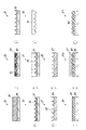
図7は、実施形態に係る拡散板の製造方法の一例を説明する図である。拡散板1の製造工程は、レンズアレイ3のマスター型を作製するマスター型作製工程(J1~J3)と、電鋳型を作製する電鋳型作製工程(J4~J6)と、二次型を作製する二次型作製工程(J7、J8)と、ガラス基板上の樹脂を成形するインプリント工程(J9~J11)とを含む。
図8は、本開示の実施形態に係る発光デバイス及びセンサモジュールを示す図である。本実施形態の発光デバイス50は、発光素子51と、発光素子51が照射する光の経路上に位置する拡散板1とを備える。拡散板1のレンズ面(レンズアレイ3)は発光素子51側を向いていてもよい。発光素子51はレーザー光を出力するが、非レーザー光を照射する構成であってもよい。発光素子51は、キャビティ構造を有するパッケージ52に収容され、拡散板1はパッケージ52に接合されていてもよい。拡散板1は、パッケージ52のリッドを兼ねてもよい。
2 透明基板
3 レンズアレイ
10 単レンズ
D ピッチ
O1 光軸
Hmax 最大縦寸
Wmax 最大幅
E1 縁部
50 発光デバイス
51 発光素子
52 パッケージ
60 受光デバイス
61 受光素子
70 モジュール用基板
100 センサモジュール
Claims (8)
- 複数の単レンズを有するレンズアレイを備え、
前記単レンズは、式(1)、式(2)、式(3)を満たす拡散板。

- 複数の単レンズを有するレンズアレイを備え、
前記単レンズは、式(1)、式(3)を満たし、かつ、前記単レンズの光軸に平行に入射された光線が、当該単レンズの縁部に当たらない拡散板。

- k≧-0.96である、請求項1又は請求項2に記載の拡散板。
- -0.96≧k≧-1である、請求項1又は請求項2に記載の拡散板。
- 前記レンズアレイが接合される透明基板を更に備え、
前記単レンズの屈折率nは、1.4≦n≦1.6である、請求項1から請求項4のいずれか一項に記載の拡散板。 - 前記レンズアレイはシリコーン樹脂から構成される、請求項5記載の拡散板。
- 発光素子と、
前記発光素子が出射する光の経路上に位置する請求項1から請求項6のいずれか一項に記載の拡散板と、
を備える発光デバイス。 - 請求項7記載の発光デバイスと、
前記発光デバイスの出射した光を受光可能な受光デバイスと、
を備えるセンサモジュール。
Priority Applications (4)
| Application Number | Priority Date | Filing Date | Title |
|---|---|---|---|
| JP2022571555A JP7483948B2 (ja) | 2020-12-23 | 2021-12-22 | 拡散板、発光デバイス及びセンサモジュール |
| US18/268,358 US20240027656A1 (en) | 2020-12-23 | 2021-12-22 | Diffuser, light-emitting device, and sensor module |
| CN202180084789.1A CN116601431A (zh) | 2020-12-23 | 2021-12-22 | 扩散板、发光器件以及传感器模块 |
| EP21910865.1A EP4270064A1 (en) | 2020-12-23 | 2021-12-22 | Diffusion plate, light-emitting device, and sensor module |
Applications Claiming Priority (2)
| Application Number | Priority Date | Filing Date | Title |
|---|---|---|---|
| JP2020213993 | 2020-12-23 | ||
| JP2020-213993 | 2020-12-23 |
Publications (1)
| Publication Number | Publication Date |
|---|---|
| WO2022138725A1 true WO2022138725A1 (ja) | 2022-06-30 |
Family
ID=82157015
Family Applications (1)
| Application Number | Title | Priority Date | Filing Date |
|---|---|---|---|
| PCT/JP2021/047589 WO2022138725A1 (ja) | 2020-12-23 | 2021-12-22 | 拡散板、発光デバイス及びセンサモジュール |
Country Status (4)
| Country | Link |
|---|---|
| US (1) | US20240027656A1 (ja) |
| EP (1) | EP4270064A1 (ja) |
| CN (1) | CN116601431A (ja) |
| WO (1) | WO2022138725A1 (ja) |
Citations (5)
| Publication number | Priority date | Publication date | Assignee | Title |
|---|---|---|---|---|
| WO2006036032A1 (ja) * | 2004-09-30 | 2006-04-06 | Sony Corporation | 光学シート、バックライトおよび液晶表示装置 |
| JP2012199063A (ja) * | 2011-03-22 | 2012-10-18 | Toppan Printing Co Ltd | 照明装置及びそれを備えた液晶ディスプレイ装置 |
| WO2015182619A1 (ja) * | 2014-05-27 | 2015-12-03 | ナルックス株式会社 | マイクロレンズアレイ及びマイクロレンズアレイを含む光学系 |
| JP2017026662A (ja) | 2015-07-16 | 2017-02-02 | デクセリアルズ株式会社 | 拡散板、表示装置、投影装置及び照明装置 |
| JP2020064088A (ja) * | 2017-02-24 | 2020-04-23 | コニカミノルタ株式会社 | 波長変換部材及び画像形成装置 |
-
2021
- 2021-12-22 WO PCT/JP2021/047589 patent/WO2022138725A1/ja active Application Filing
- 2021-12-22 CN CN202180084789.1A patent/CN116601431A/zh active Pending
- 2021-12-22 EP EP21910865.1A patent/EP4270064A1/en active Pending
- 2021-12-22 US US18/268,358 patent/US20240027656A1/en active Pending
Patent Citations (5)
| Publication number | Priority date | Publication date | Assignee | Title |
|---|---|---|---|---|
| WO2006036032A1 (ja) * | 2004-09-30 | 2006-04-06 | Sony Corporation | 光学シート、バックライトおよび液晶表示装置 |
| JP2012199063A (ja) * | 2011-03-22 | 2012-10-18 | Toppan Printing Co Ltd | 照明装置及びそれを備えた液晶ディスプレイ装置 |
| WO2015182619A1 (ja) * | 2014-05-27 | 2015-12-03 | ナルックス株式会社 | マイクロレンズアレイ及びマイクロレンズアレイを含む光学系 |
| JP2017026662A (ja) | 2015-07-16 | 2017-02-02 | デクセリアルズ株式会社 | 拡散板、表示装置、投影装置及び照明装置 |
| JP2020064088A (ja) * | 2017-02-24 | 2020-04-23 | コニカミノルタ株式会社 | 波長変換部材及び画像形成装置 |
Also Published As
| Publication number | Publication date |
|---|---|
| EP4270064A1 (en) | 2023-11-01 |
| CN116601431A (zh) | 2023-08-15 |
| US20240027656A1 (en) | 2024-01-25 |
| JPWO2022138725A1 (ja) | 2022-06-30 |
Similar Documents
| Publication | Publication Date | Title |
|---|---|---|
| CN107430219B (zh) | 扩散板 | |
| US20200117019A1 (en) | Diffuser plate and method for designing diffuser plate | |
| KR102136021B1 (ko) | 확산판 및 투영식 프로젝터 장치 | |
| US11163175B2 (en) | Device for forming a field intensity pattern in the near zone, from incident electromagnetic waves | |
| US8529075B2 (en) | Antireflection structure, optical unit, and optical device | |
| CN109633946B (zh) | 一种显示装置、其制作方法及3d打印系统 | |
| WO2016163125A1 (ja) | 複合拡散板 | |
| CN110161602B (zh) | 漫射板、漫射板的设计方法、显示装置、投影装置和照明装置 | |
| US20150070870A1 (en) | Illumination system | |
| JP6804830B2 (ja) | 拡散板 | |
| US8411379B2 (en) | Optical device and associated methods | |
| US11726237B2 (en) | Light diffuser plate, image display device, and lighting device | |
| TW200411226A (en) | Light guide plate and method of making the same | |
| JPH09307697A (ja) | マイクロレンズアレイおよびイメージセンサおよび光画像伝送素子 | |
| CN114200556B (zh) | 微光学透镜、制备方法及显示系统 | |
| WO2022138725A1 (ja) | 拡散板、発光デバイス及びセンサモジュール | |
| TWM626901U (zh) | 三維列印裝置及其光源模組 | |
| JP7483948B2 (ja) | 拡散板、発光デバイス及びセンサモジュール | |
| CN216387438U (zh) | 组合式微透镜阵列匀光结构及装设有该结构的镜头、设备 | |
| TW202034022A (zh) | 擴散板 | |
| CN211148968U (zh) | 红外光扩散片和光学系统 | |
| US20200161492A1 (en) | Light distribution plate for uniform irradiance of compact photovoltaic arrays | |
| EP3633421A1 (en) | Effective refractive index based device for forming at least one focused beam in the near zone, from incident electromagnetic waves | |
| CN216718826U (zh) | 出光模组及tof成像装置 | |
| WO2023171589A1 (ja) | 拡散板、発光デバイス及びセンサモジュール |
Legal Events
| Date | Code | Title | Description |
|---|---|---|---|
| 121 | Ep: the epo has been informed by wipo that ep was designated in this application |
Ref document number: 21910865 Country of ref document: EP Kind code of ref document: A1 |
|
| ENP | Entry into the national phase |
Ref document number: 2022571555 Country of ref document: JP Kind code of ref document: A |
|
| WWE | Wipo information: entry into national phase |
Ref document number: 202180084789.1 Country of ref document: CN |
|
| WWE | Wipo information: entry into national phase |
Ref document number: 18268358 Country of ref document: US |
|
| NENP | Non-entry into the national phase |
Ref country code: DE |
|
| ENP | Entry into the national phase |
Ref document number: 2021910865 Country of ref document: EP Effective date: 20230724 |