EP4539643A1 - Anzeigesubstrat und herstellungsverfahren dafür sowie anzeigevorrichtung - Google Patents
Anzeigesubstrat und herstellungsverfahren dafür sowie anzeigevorrichtung Download PDFInfo
- Publication number
- EP4539643A1 EP4539643A1 EP22947328.5A EP22947328A EP4539643A1 EP 4539643 A1 EP4539643 A1 EP 4539643A1 EP 22947328 A EP22947328 A EP 22947328A EP 4539643 A1 EP4539643 A1 EP 4539643A1
- Authority
- EP
- European Patent Office
- Prior art keywords
- voltage
- power supply
- lines
- line
- low
- Prior art date
- Legal status (The legal status is an assumption and is not a legal conclusion. Google has not performed a legal analysis and makes no representation as to the accuracy of the status listed.)
- Pending
Links
Images


Classifications
-
- H—ELECTRICITY
- H10—SEMICONDUCTOR DEVICES; ELECTRIC SOLID-STATE DEVICES NOT OTHERWISE PROVIDED FOR
- H10K—ORGANIC ELECTRIC SOLID-STATE DEVICES
- H10K59/00—Integrated devices, or assemblies of multiple devices, comprising at least one organic light-emitting element covered by group H10K50/00
- H10K59/10—OLED displays
- H10K59/12—Active-matrix OLED [AMOLED] displays
- H10K59/131—Interconnections, e.g. wiring lines or terminals
- H10K59/1315—Interconnections, e.g. wiring lines or terminals comprising structures specially adapted for lowering the resistance
-
- H—ELECTRICITY
- H10—SEMICONDUCTOR DEVICES; ELECTRIC SOLID-STATE DEVICES NOT OTHERWISE PROVIDED FOR
- H10K—ORGANIC ELECTRIC SOLID-STATE DEVICES
- H10K59/00—Integrated devices, or assemblies of multiple devices, comprising at least one organic light-emitting element covered by group H10K50/00
- H10K59/80—Constructional details
- H10K59/805—Electrodes
- H10K59/8052—Cathodes
- H10K59/80521—Cathodes characterised by their shape
Definitions
- OLEDs Organic light emitting diodes
- QLEDs quantum-dot light emitting diodes
- TFTs thin film transistors
- the present disclosure provides a display substrate including a display area, which includes a plurality of pixel regions and a plurality of blank regions, wherein the blank regions are arranged between adjacent pixel regions in a first direction and between adjacent pixel regions in a second direction, the first direction intersects the second direction, the pixel regions are configured to display images, and the blank regions are configured to transmit light; in a plane perpendicular to the display substrate, the display substrate includes a driving circuit layer disposed on a substrate and a light emitting structure layer disposed on a side of the driving circuit layer away from the substrate, the driving circuit layer of a pixel region includes a plurality of circuit units, a plurality of first power supply lines and at least one second power supply line, a the circuit unit at least includes a pixel driving circuit, the light emitting structure layer of the pixel region at least includes a patterned cathode, the area of an orthographic projection of the cathode on the substrate is 1.1 to 1.3 times the area of an orthographic projection of the
- the high-voltage power supply connecting lines include first high-voltage connecting lines extending along the first direction and second high-voltage connecting lines extending along the second direction; the first high-voltage connecting lines are connected to the first power supply lines in the adjacent pixel regions in the first direction respectively, and the second high-voltage connecting lines are connected to the first power supply lines in the adjacent pixel regions in the second direction respectively; the driving circuit layer includes a plurality of conductive layers, the first high-voltage connecting lines are disposed in at least two of the conductive layers, and the second high-voltage connecting lines are disposed in at least two of the conductive layers.
- the pixel driving circuit includes a storage capacitor including a first plate and a second plate, an orthographic projection of the first plate on the substrate overlapping at least partially with an orthographic projection of the second plate on the substrate, and the second plate being connected to the first power supply lines;
- the first high-voltage connecting lines include a first transverse connecting line, which is connected to the second plates in the adjacent pixel regions in the first direction respectively, and the first transverse connecting line and the second plates are disposed in the same layer and are connected to each other to form an integrated structure.
- the first high-voltage connecting lines further include a second transverse connecting line, the second transverse connecting line and the first transverse connecting line are disposed in different conductive layers, both ends of the second transverse connecting line in the first direction are connected to both ends of the first transverse connecting line in the first direction through via holes respectively, and an orthographic projection of the second transverse connecting line on the substrate overlaps at least partially with an orthographic projection of the first transverse connecting line on the substrate.
- the third transverse connecting line includes at least two first sub-lines extending along the first direction and at least two second sub-lines extending along the second direction, the at least two second sub-lines are respectively connected to both ends of the at least two first sub-lines to form a mesh in the blank region, and an orthographic projection of at least one of the first sub-lines on the substrate overlaps at least partially with the orthographic projection of the second transverse connecting line on the substrate.
- the second high-voltage connecting lines include at least one first vertical connecting line, the first vertical connecting line is connected to the first power supply lines in the adjacent pixel regions in the second direction respectively, and the first vertical connecting line and the first power supply line are disposed in the same layer and are connected to each other to form an integrated structure.
- the second high-voltage connecting lines further include at least one second vertical connecting line, the second vertical connecting line and the first vertical connecting line are disposed in different conductive layers, the second vertical connecting line is connected to the first power supply lines in the adjacent pixel regions in the second direction respectively, and an orthographic projection of the second vertical connecting line on the substrate overlaps at least partially with an orthographic projection of the first vertical connecting line on the substrate.
- the pixel region further includes a high-voltage mesh line, the first power supply line and the high-voltage grid line are disposed in different conductive layers, the high-voltage grid line is connected to the first power supply line through a via hole, and an orthographic projection of the high-voltage grid line on the substrate overlaps at least partially with an orthographic projection of the first power supply line on the substrate.
- the high-voltage mesh line and the second vertical connecting line of the second high-voltage connecting lines are disposed in the same layer and are connected to each other to form an integrated structure.
- the high-voltage mesh line includes at least two first mesh lines extending along the first direction and a plurality of second mesh lines extending along the second direction, the at least two first mesh lines are connected to both ends of the plurality of second mesh lines respectively, an orthographic projection of the second mesh line on the substrate overlaps at least partially with the orthographic projection of the first power supply line on the substrate, and the second mesh lines are connected to the first power supply line through via holes.
- the low-voltage power supply connecting lines include first low-voltage connecting lines extending along the first direction and second low-voltage connecting lines extending along the second direction; the second low-voltage connecting lines are connected to the second power supply lines in the adjacent pixel regions in the second direction respectively, and the first low-voltage connecting lines are connected to adjacent second low-voltage connecting lines in the first direction respectively; the driving circuit layer includes a plurality of conductive layers, and the first low-voltage connecting lines and the second low-voltage connecting lines are disposed in the same conductive layer.
- the second low-voltage connecting lines at least include a third vertical connecting line, which includes a plurality of third sub-lines extending along the second direction and at least two third connection blocks, the at least two third connection blocks being connected to both ends of the at least two third sub-lines.
- the cathode is connected to the cathode connection electrodes through cathode electrode openings.
- the display substrate further includes a bonding area located at a side of the display area in the second direction and a bezel area located at other sides of the display area, the bezel area including a top bezel region located at a side of the display area away from the bonding area and a side bezel region located at one or two sides of the display area in the first direction; a bonding high-voltage lead and a bonding low-voltage lead are provided in the bonding area, a top bezel high-voltage lead and a top bezel low-voltage lead are provided in the top bezel region, and a side bezel high-voltage lead and a side bezel low-voltage lead are provided in the side bezel region; the bonding high-voltage lead is connected to the side bezel high-voltage lead and the side bezel high-voltage lead is connected to the top bezel high-voltage lead to form an annular high-voltage lead surrounding the display area; the bonding low-voltage lead is connected to the side bezel low-volt
- the annular low-voltage lead is located at a side of the annular high-voltage lead away from the display area.
- the top bezel region in the plane perpendicular to the display substrate, includes a plurality of conductive layers, the top bezel high-voltage lead and the top bezel low-voltage lead are disposed in at least two of the conductive layers, the top bezel high-voltage lead is connected to the high-voltage power supply wiring in the display area through a high-voltage connecting line on one of the at least two of the conductive layers, and the top bezel low-voltage lead is connected to the low-voltage power supply wiring in the display area through a low-voltage connecting line in the other one of the at least two of the conductive layers.
- the side bezel region in the plane perpendicular to the display substrate, includes a plurality of conductive layers, the side bezel high-voltage lead and the side bezel low-voltage lead are disposed in at least two of the conductive layers, the side bezel high-voltage lead is connected to the high-voltage power supply wiring in the display area through a high-voltage connecting line in one of the at least two of the conductive layers, and the side bezel low-voltage lead is connected to the low-voltage power supply wiring in the display area through a low-voltage connecting line in the other one of the at least two of the conductive layers.
- the bonding area in the plane perpendicular to the display substrate, includes a plurality of conductive layers, the bonding high-voltage lead is disposed in at least two of the conductive layers, and the bonding low-voltage lead is disposed in at least two of the conductive layers.
- the present disclosure further provides a display device including the display substrate described above.
- Scales of the drawings in the present disclosure can be used as references in the actual processes, but are not limited thereto.
- the width-to-length ratio of a channel, the thickness of each film layer and the spacing between two film layers, and the width of each signal line and the spacing between two signal lines can be adjusted according to actual needs.
- the quantity of pixels in a display substrate and the quantity of sub-pixels in each pixel are not limited to the number shown in the drawings.
- the drawings described in the present disclosure are a schematic structure diagram only, and one implementation of the present disclosure is not limited to the shapes or numerical values shown in the drawings.
- orientation or position relationships are used in the specification to illustrate position relationships between the constituent elements with reference to the drawings, and are intended to facilitate description of the specification and simplification of the description, but not to indicate or imply that the mentioned device or element must have a specific orientation or be constructed and operated in a specific orientation, therefore, they should not be understood as limitations to the present disclosure.
- the position relationships between the constituent elements are appropriately changed according to directions of the constituent elements described. Therefore, words and phrases used in the specification are not limited and appropriate substitutions may be made according to situations.
- connection may be a fixed connection, a detachable connection or an integrated connection, or may be a mechanical connection or an electrical connection, or may be a direct connection, an indirect connection through intermediate components, or communication inside two components.
- connection may be a fixed connection, a detachable connection or an integrated connection, or may be a mechanical connection or an electrical connection, or may be a direct connection, an indirect connection through intermediate components, or communication inside two components.
- a transistor refers to a component which at least includes three terminals, a gate electrode, a drain electrode and a source electrode.
- the transistor has a channel region between the drain electrode (drain electrode terminal, drain region or drain) and the source electrode (source electrode terminal, source region or source), and a current can flow through the drain electrode, the channel region and the source electrode.
- the channel region refers to a region which the current flows mainly through.
- the first electrode may be a drain electrode and the second electrode may be a source electrode, or the first electrode may be a source electrode and the second electrode may be a drain electrode.
- the "source electrode” and the “drain electrode” may be interchangeable and a “source terminal” and "a drain terminal” may be interchangeable.
- parallel refers to a state in which an angle formed by two straight lines is greater than -10° and less than 10°, and thus also includes a state in which the angle is greater than -5° and less than 5°.
- vertical refers to a state in which an angle formed by two straight lines is greater than 80° and less than 100°, and thus also includes a state in which the angle is greater than 85° and less than 95°.
- Triangle, rectangle, trapezoid, pentagon or hexagon in the specification are not in the strict sense, and they may be approximate triangle, rectangle, trapezoid, pentagon or hexagon, in which there may be some small deformation caused by tolerance, or there may be chamfers, arc edges and deformation, etc.
- “About” in the present disclosure means that a boundary is defined loosely and numerical values in process and measurement error ranges are allowed.
- FIG. 1 is a schematic structure diagram of a display device.
- the display device may include a time sequence controller, a data driver, a scan driver, a light emitting driver and a pixel array.
- the time sequence controller is connected to the data driver, the scan driver and the light emitting driver respectively
- the data driver is connected to a plurality of data signal lines (D1 to Dn) respectively
- the scan driver is connected to a plurality of scan signal lines (S1 to Sm) respectively
- the light emitting driver is connected to a plurality of light emitting control signal lines (E1 to Eo) respectively.
- the pixel array may include a plurality of sub-pixels Pxij, wherein i and j may be natural numbers.
- the data driver may sample the grayscale values using the clock signals and apply the data voltages corresponding to the grayscale values to the data signal lines D1 to Dn by taking a row of sub-pixels as a unit, wherein n may be a natural number.
- the scan driver may generate scan signals to be provided to the scan signal lines S1, S2, S3, ..., and Sm by receiving the clock signals and the scan start signals from the time sequence controller. For example, the scan driver may sequentially provide scan signals with on-level pulse to the scan signal lines S1 to Sm.
- the scan driver may be constructed in the form of a shift register and generate the scan signals by sequentially transmitting the scan start signals provided in the form of an on-level pulse to a next-stage circuit under the control of the clock signals, wherein m may be a natural number.
- the light emitting driver may generate emission signals to be provided to the light emitting control signal lines E1, E2, E3, ..., and Eo by receiving the clock signals and the emission stop signals from the time sequence controller.
- the light emitting driver may sequentially provide emission signals with off-level pulse to the light emitting control signal lines E1 to Eo.
- the light emitting driver may be constructed in the form of a shift register and generate the emission signals by sequentially transmitting the emission stop signals provided in the form of an off-level pulse to a next-stage circuit under the control of the clock signals, wherein o may be a natural number.
- FIG. 2 is a schematic structure diagram of a display substrate.
- the display substrate may include a display area 100, a bonding area 200 located at one side of the display area 100 and a bezel area 300 located at other sides of the display area 100.
- the display area 100 may be a flat area including a plurality of sub-pixels Pxij that form a pixel array.
- the plurality of sub-pixels Pxij is configured to display dynamic pictures or static images.
- the display area 100 may be referred to as an active area (AA).
- the display substrate may be deformable, e.g., curled, crooked, folded or rolled-up.
- the bonding area 200 may include a fan-out region, a bending region, a driver chip region and a bonding pin region that are arranged sequentially along a direction away from the display area 100.
- the fan-out region which is connected to the display area 100, may at least include data fan-out lines.
- a plurality of data fan-out lines is configured to be connected to the data signal lines in the display area.
- the bending region which is connected to the fan-out region, may include a composite insulating layer, in which grooves are provided, and the bending region is configured to cause the bonding area to bend to the back of the display area.
- the driver chip region may at least include an integrated circuit (IC), and be configured to be connected to the plurality of data fan-out lines.
- the bonding pin region may at least include a plurality of bonding pads, and be configured to be bound to an external flexible printed circuit (FPC).
- FPC flexible printed circuit
- the bezel area 300 may include a circuit region, a power supply line region, a crack dam zone and a cutting region which are sequentially arranged along the direction away from the display area 100.
- the circuit region which is connected to the display area 100, may at least include a gate driving circuit which is connected to a first scan line, a second scan line and a light emitting control signal line of the pixel driving circuit in the display area 100.
- the power supply line region which is connected to the circuit region, may at least include a bezel power supply lead, the bezel power supply lead extends along a direction parallel to an edge of the display area and is connected to a cathode in the display area 100.
- a first isolation dam and a second isolation dam may be provided in the fan-out region in the bonding area 200 and the power supply line region in the bezel area 300.
- the first isolation dam and the second isolation dam may extend in the direction parallel to the edge of the display area 100 to form an annular structure surrounding the display area 100.
- the edge of the display area is an edge at one side of the bonding area or the bezel area of the display area.
- the substrate 101 may be a flexible substrate or a rigid substrate.
- the driving circuit layer 102 may include a plurality of circuit units, each of which may include a pixel driving circuit formed by a plurality of transistors and a storage capacitor.
- the light emitting structure layer 103 may include a plurality of sub-pixels, each of which may include a light emitting device and a pixel definition layer 302.
- the light emitting device may include an anode 301, an organic light emitting layer 303 and a cathode 304.
- the anode 301 is connected to the pixel driving circuit of the corresponding circuit unit
- the organic light emitting layer 303 is connected to the anode 301
- the cathode 304 is connected to the organic light emitting layer 303.
- the organic light emitting layer 303 emits light of a corresponding color under driving of the anode 301 and the cathode 304.
- the encapsulation structure layer 104 may include a first encapsulation layer 401, a second encapsulation layer 402 and a third encapsulation layer 403 that are stacked.
- the first encapsulation layer 401 and the third encapsulation layer 403 may be made of inorganic materials
- the second encapsulation layer 402 may be made of an organic material.
- the second encapsulation layer 402 is disposed between the first encapsulation layer 401 and the third encapsulation layer 403 to form a stacked structure of inorganic material/organic material/inorganic material, so as to ensure that external water vapor cannot enter the light emitting structure layer 103.
- the organic light emitting layer may include a light emitting layer (EML) and any one or more of a hole injection layer (HIL), a hole transport layer (HTL), an electron block layer (EBL), a hole block layer (HBL), an electron transport layer (ETL) and an electron injection layer (EIL).
- EML light emitting layer
- HIL hole injection layer
- HTL hole transport layer
- EBL electron block layer
- HBL hole block layer
- ETL electron transport layer
- ETL electron transport layer
- EIL electron injection layer
- one or more of hole injection layers, hole transport layers, electron block layers, hole block layers, electron transport layers and electron injection layers of all sub-pixels may be connected to each other to form a common layer.
- Light emitting layers of adjacent circuit units may overlap with each other slightly, or may isolate from each other.
- the pixel driving circuit may include a first node N1, a second node N2 and a third node N3.
- the first node N1 is connected to a first electrode of the third transistor T3, a second electrode of the fourth transistor T4 and a second electrode of the fifth transistor T5 respectively
- the second node N2 is connected to a second electrode of the first transistor, a first electrode of the second transistor T2, a control electrode of the third transistor T3 and a second end of the storage capacitor C respectively
- the third node N3 is connected to a second electrode of the second transistor T2, a second electrode of the third transistor T3 and a first electrode of the sixth transistor T6 respectively.
- a control electrode of the first transistor T1 is connected to the second scan signal line S2, a first electrode of the first transistor T1 is connected to the first initial signal line INIT1, and the second electrode of the first transistor is connected to the second node N2.
- the first transistor T1 will transmit a first initial voltage to the second end of the storage capacitor C and the control electrode of the third transistor T3 so as to initialize charge quantities of the storage capacitor C and the control electrode of the third transistor T3.
- a control electrode of the second transistor T2 is connected to the first scan signal line S1, the first electrode of the second transistor T2 is connected to the second node N2, and a second electrode of the second transistor T2 is connected to the third node N3.
- the second transistor T2 will cause the control electrode of the third transistor T3 to be connected to the second electrode of the third transistor T3.
- the light emitting device may be an OLED including a first electrode (anode), an organic light emitting layer and a second electrode (cathode) which are stacked, or may be a QLED including a first electrode (anode), a quantum dot light emitting layer and a second electrode (cathode) which are stacked.
- the first transistor T1 through the seventh transistor T7 may be low temperature poly-silicon thin film transistors, or may be oxide thin film transistors, or may be low temperature poly-silicon thin film transistors and oxide thin film transistors.
- Active layers of the low temperature poly-silicon thin film transistors may be made of low temperature poly-silicon (LTPS), and active layers of the oxide thin film transistors may be made of oxide semiconductor (Oxide).
- LTPS low temperature poly-silicon
- Oxide oxide semiconductor
- the low temperature poly-silicon thin film transistors have advantages such as high migration rate and fast charging.
- the oxide thin film transistors have advantages such as low leakage current.
- the low temperature poly-silicon thin film transistors and the oxide thin film transistors are integrated on one display substrate to form a low temperature polycrystalline oxide (LTPO) display substrate, so that the advantages of both the low temperature poly-silicon thin film transistor and the oxide thin film transistors can be utilized, to implement low-frequency driving, decrease power consumption, and improve display quality.
- LTPO low temperature polycrystalline oxide
- a second stage A2 referred to as a data writing stage or a threshold compensation stage
- the signal of the first scan signal line S1 is a low-level signal
- signals of the second scan signal line S2 and the light emitting control signal line E are high-level signals
- the data signal line D outputs a data voltage.
- the third transistor T3 is turned on.
- the signal of the first scan signal line S1 is a low-level signal, so that the second transistor T2, the fourth transistor T4 and the seventh transistor T7 are turned on.
- the second transistor T2 and the fourth transistor T4 are turned on, so that the data voltage output by the data signal line D is provided to the second node N2 through the first node N1, the turned-on third transistor T3, the third node N3 and the turned-on second transistor T2, and a difference between the data voltage output by the data signal line D and a threshold voltage of the third transistor T3 is charged to the storage capacitor C.
- a voltage of the second end (the second node N2) of the storage capacitor C is Vd-IVthl, wherein Vd is the data voltage output by the data signal line D, and Vth is the threshold voltage of the third transistor T3.
- the signal of the light emitting control signal line E is a low-level signal, and the signals of the first scan signal line S1 and the second scan signal line S2 are high-level signals.
- the signal of the light emitting control signal line E is a low-level signal, so that the fifth transistor T5 and the sixth transistor T6 are turned on, and a power supply voltage output by the first power supply line VDD provides a drive voltage to the first electrode of the OLED through the turned-on fifth transistor T5, third transistor T3 and sixth transistor T6 to drive the OLED to emit light.
- the transparent display which is an important personalized display field of the display technology, means that a display device itself has a certain degree of light penetration.
- the display device can display images in a transparent state, so that a viewer can see not only video images in the display device, but also scenes behind the display device.
- the transparent display may be widely applied to outdoor display or vehicle-mounted display.
- FIG. 5 is a schematic diagram of a planar structure of a display area in a transparent display substrate.
- the display area may include a plurality of pixel regions PD and a plurality of blank regions PB.
- the pixel regions PD and the blank regions PB are alternately arranged in the first direction X and the pixel regions PD and the blank regions PB are alternately arranged in the second direction Y, such that a blank region PB is arranged both between adjacent pixel regions PD in the first direction X and between adjacent pixel regions PD in the second direction Y, the first direction X intersecting the second direction Y.
- the pixel regions PD are configured to implement display of images
- the blank regions PB are configured to implement transmission of light, so as to implement transparent display.
- FIG. 7 is a schematic diagram of a planar structure of a light emitting structure layer in a pixel region.
- the light emitting structure layer of at least one pixel region PD may include a first sub-pixel P1 emitting light of a first color, a second sub-pixel P2 emitting light of a second color and a third sub-pixel P3 emitting light of a third color.
- Each sub-pixel may include a light emitting device, which is connected to the pixel driving circuit of the corresponding circuit unit and configured to emit light of corresponding luminance in response to a current output by the pixel driving circuit to which the light emitting circuit is connected.
- the first sub-pixel P1 may be a red (R) sub-pixel emitting red light
- the second sub-pixel P2 may be a blue (B) sub-pixel emitting blue light
- the third sub-pixel P3 may be a green (G) sub-pixel emitting green light.
- the sub-pixels may be in the shape of a rectangle, a rhombus, a pentagon or hexagon.
- the driving circuit layer of the pixel region PD may include four circuit units, and the light emitting structure layer of the pixel region PD may include four sub-pixels.
- the four circuit units and the four sub-pixels may be arranged side by side horizontally, side by side vertically, in the shape of a square or in the shape of a diamond, the present disclosure is not limited thereto.
- the circuit unit mentioned in the present disclosure refers to an area divided according to the pixel driving circuit
- the sub-pixel mentioned in the present disclosure refers to an area divided according to the light emitting device.
- the positions and shapes of orthographic projections of the sub-pixels on the substrate may correspond to the positions and shapes of orthographic projections of the circuit units on the substrate, or the positions and shapes of the orthographic projections of the sub-pixels on the substrate may not correspond to the positions and shapes of the orthographic projections of the circuit units on the substrate.
- An exemplary embodiment of the present disclosure provides a display substrate, which implements transparent display, including a display area, the display area includes a plurality of pixel regions and a plurality of blank regions, wherein a blank region is arranged between its adjacent pixel regions in a first direction and between its adjacent pixel regions arranged in a second direction, the first direction intersects the second direction, the pixel regions are configured to display images, and the blank regions are configured to transmit light; in a plane perpendicular to the display substrate, the display substrate includes a driving circuit layer disposed on a substrate and a light emitting structure layer disposed on one side of the driving circuit layer away from the substrate, the driving circuit layer of the pixel region includes a plurality of circuit units, a plurality of first power supply lines and at least one second power supply line, each of the circuit units at least includes a pixel driving circuit, the light emitting structure layer of the pixel region includes a patterned cathode, the area of an orthographic projection of the cathode on the substrate is 1.1 to
- the high-voltage power supply connecting lines include first high-voltage connecting lines extending along the first direction and second high-voltage connecting lines extending along the second direction; the first high-voltage connecting lines are connected to the first power supply lines in the adjacent pixel regions in the first direction respectively, and the second high-voltage connecting lines are connected to the first power supply lines in the adjacent pixel regions in the second direction respectively; the driving circuit layer includes a plurality of conductive layers, the first high-voltage connecting lines are disposed in at least two of the conductive layers, and the second high-voltage connecting lines are disposed in at least two of the conductive layers.
- a extending along a direction B means that A may include a primary portion, which is a line, a line segment or a strip-shaped body, and a secondary portion connected to the primary portion.
- the primary portion extends along the direction B, and the length of the primary portion extending along the direction B is greater than the length of the secondary portion extending along other directions.
- a extending along the direction B mentioned in the following description means that "the primary portion of A extends along the direction B".
- the second direction Y may be a direction from the display area towards the bonding area, and the opposite direction of the second direction Y may be a direction from the bonding area towards the display area.
- the patterned cathode 304 refers to a blocky structure processed through patterning.
- a main area, which is relatively large in area, in the cathode 304 of the blocky structure is provided in an area where the pixel region PD is located, and a connection area or other areas, which are relatively small in area, in the cathode 304 are provided in an area where the blank region PB is located, that is, the cathode 304 is not provided in the larger area of the blank region PB, so as to improve the transmittance of the display substrate.
- an orthographic projection of the cathode 304 on the substrate may contain an orthographic projection of the pixel region PD on the substrate.
- the orthographic projection of the patterned cathode 304 on the substrate has a cathode projection area, and the orthographic projection of the pixel region PD on the substrate has a pixel region projection area.
- the cathode projection area may be about 1.1 to 1.3 times the pixel region projection area.
- the driving circuit layer of the blank region PB may include at least one high-voltage power supply connecting line configured to be connected to the first power supply lines 70 in the adjacent pixel regions PD and at least one low-voltage power supply connecting line configured to be connected to the second power supply lines 80 in the adjacent pixel regions PD.
- the high-voltage power supply connecting line may include a first high-voltage connecting line extending along the first direction X and a second high-voltage connecting line extending along the second direction Y.
- the first high-voltage connecting line is configured to be connected to the first power supply lines 70 in the adjacent pixel regions PD in the first direction X, to implement continuous transmission by the first power supply lines 70 in the first direction X
- the second high-voltage connecting line is configured to be connected to the first power supply lines 70 in the adjacent pixel region PD in the second direction Y, to implement continuous transmission by the first power supply lines 70 in the second direction Y.
- the first power supply lines 70, the first high-voltage connecting line and the second high-voltage connecting line form a high-voltage power supply wiring with a mesh connection structure in the display area, through high-voltage power supply wiring, high-voltage power supply signals are transmitted.
- the second power supply line 80, the first low-voltage connecting line and the second low-voltage connecting line form a low-voltage power supply wiring with a mesh connection structure in the display area, through the low-voltage power supply wiring, low-voltage power supply signals are transmitted.
- the driving circuit layer may include a plurality of conductive layers.
- the first high-voltage connecting line and the second high-voltage connecting line may be disposed in at least two of the conductive layers, to form a high-voltage power supply wiring of a double-layer structure in the display area, and the high-voltage power supply wiring in each layer have a mesh connection structure.
- the first low-voltage connecting line and the second low-voltage connecting line may be disposed in the same conductive layer and formed synchronously through the same running of patterning processes.
- the plurality of conductive layers of the driving circuit layer may at least include a first conductive layer, a second conductive layer, a third conductive layer and a fourth conductive layer disposed in sequence on the substrate.
- the first high-voltage connecting line and the second high-voltage connecting line may be respectively disposed in the second conductive layer, the third conductive layer and the fourth conductive layer, and the first low-voltage connecting line and the second low-voltage connecting line may be disposed in the fourth conductive layer.
- the storage capacitor may include a first plate and a second plate 33.
- the first power supply lines 70 are connected to the second plate 33.
- the second plates 33 of the three pixel driving circuits in the pixel region are connected to each other to form an integrated structure.
- the first scan signal line 21, the second scan signal line 22, the light emitting control signal line 23, the first initial signal line 31 and the second initial signal line 32 may be in the shape of a straight line or a fold line, which extends along the first direction X
- the first power supply line 70 and the data signal line 45 may be in the shape of a straight line or a fold line, which extends along the second direction Y.
- a plurality of signal lines in one pixel region may be connected to a plurality of signal lines in another adjacent pixel region through a plurality of blank region connecting lines in a blank region, to implement continuous transmission by the plurality of signal lines in the first direction X and the second direction Y.
- the plurality of blank region connecting lines in the blank region may at least include a first scan line connecting line 61 connected to the first scan signal lines 21 in the adjacent pixel regions in the first direction X, a second scan line connecting line 62 connected to the second scan signal lines 22 in the adjacent pixel regions in the first direction X, a light emitting control connecting line 63 connected to the light emitting control signal lines 23 in the adjacent pixel regions in the first direction X, a first initial transverse connecting line 64 connected the first initial signal lines 31 in the adjacent pixel regions in the first direction X, a second initial transverse connecting line 65 connected the second initial signal lines 32 in the adjacent pixel regions in the first direction X, a first high-voltage connecting line connected to the first power supply lines 70 in the adjacent pixel regions in the first direction X, a first low-voltage connecting line connected to the second power supply lines 80 in the adjacent pixel regions in the first direction X, a data signal connecting line 66 connected to the data signal lines 45 in the adjacent pixel regions in
- the first scan connecting line 61, the second scan connecting line 62, the light emitting control connecting line 63, the first initial transverse connecting line 64, the second initial transverse connecting line 65, the first high-voltage connecting line and the first low-voltage connecting line may be in the shape of a straight line or a fold line, which extends along the first direction X
- the data signal connecting line 66, the first initial connection line 47, the second initial connection line 48, the first initial vertical connecting line 67, the second initial vertical connecting line 68, the second high-voltage connecting line and the second low-voltage connecting line may be in the shape of a straight line or a fold line, which extends along the second direction Y.
- first initial connection line 47, the second initial connection line 48, the first initial vertical connecting line 67 and the second initial vertical connecting line 68 may be disposed in the third conductive layer.
- the first initial connection line 47 and the first initial vertical connecting line 67 may be connected to each other to form an integrated structure
- the second initial connection line 48 and the second initial vertical connecting line 68 may be connected to each other to form an integrated structure.
- the pixel region includes three circuit units, one first power supply line 70 being provided in each of circuit units.
- the first power supply line 70 may be in the shape of a straight line or a fold line, which extends along the second direction Y.
- the first power supply line 70 is connected to the second plate 33 of the circuit unit in which the first power supply line 70 is located.
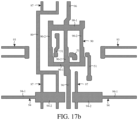
- the first high-voltage connecting line may at least include a first transverse connecting line 91, a second transverse connecting line 92 and a third transverse connecting line 93
- the first low-voltage connecting line may at least include a fourth transverse connecting line 94 and a cathode connection electrode 110
- the second high-voltage connecting line may at least include a first vertical connecting line 95 and a second vertical connecting line 96
- the second low-voltage connecting line may at least include a third vertical connecting line 97.
- the second transverse connecting line 92 may be disposed in the third conductive layer.
- An orthographic projection of the second transverse connecting line 92 on the substrate overlaps at least partially with an orthographic projection of the first transverse connecting line 91 on the substrate. Because both ends of the second transverse connecting line 92 are connected to both ends of the first transverse connecting line 91 through via holes respectively, the first transverse connecting line 91 located on the second conductive layer and the second transverse connecting line 92 located on the third conductive layer form a double-layer wiring in the blank region, by the double-layer wiring the high-voltage power supply signals are transmitted in the first direction X.
- the third transverse connecting line 93 may in the shape of a mesh, which extends along the first direction X. Both ends of the third transverse connecting line 93 in the first direction X are connected to both ends of the second transverse connecting line 92 in the first direction X respectively, to form a mesh in the shape of a rectangular ring in the blank region. Because the second transverse connecting line 92 is connected to the first power supply lines 70, the third transverse connecting line 93 may form yet another first high-voltage connecting line by which the high-voltage power supply signals are transmitted in the first direction X.
- the third transverse connecting line 93 may be disposed in the fourth conductive layer.
- An orthographic projection of the third transverse connecting line 93 on the substrate overlaps at least partially with the orthographic projection of the second transverse connecting line 92 on the substrate. Because both ends of the third transverse connecting line 93 are connected to both ends of the second transverse connecting line 92 through via holes respectively, the first transverse connecting line 91 located on the second conductive layer, the second transverse connecting line 92 located on the third conductive layer and the third transverse connecting line 93 located on the fourth conductive layer form a three-layer wiring in the blank region, by three-layer wiring the high-voltage power supply signals are transmitted in the first direction X,.
- the third transverse connecting line 93 may include at least two first sub-lines extending along the first direction X and at least two second sub-lines extending along the second direction Y.
- the at least two second sub-lines are connected to both ends of the at least two first sub-lines in the first direction X respectively, to form a mesh in the shape of a rectangular ring in the blank region.
- An orthographic projection of one of the first sub-lines on the substrate overlaps at least partially with the orthographic projection of the second transverse connecting line 92 on the substrate, and an orthographic projection of the other one of the first sub-lines on the substrate overlaps at least partially with an orthographic projection of the light emitting control connecting line 63 on the substrate.
- the first power supply lines 70 and the first vertical connecting line 95 may be disposed in the third conductive layer.
- the first power supply lines 70 and the first vertical connecting line 95 may be connected to each other to form an integrated structure.
- the second vertical connecting line 96 may be in the shape of a straight line or a fold line, which extends along the second direction Y. Because the second vertical connecting line 96 is connected to the first power supply lines 70 in the adjacent pixel regions in the second direction Y, the second vertical connecting line 96 may form another second high-voltage connecting line by which the high-voltage power supply signals are transmitted in the second direction Y.
- first power supply lines 70 may be provided in the pixel region.
- two first vertical lines 95 and one second vertical line 96 may be provided in the blank region to reduce the number of wirings in the blank region and improve the transmittance of the display substrate.
- the pixel region may further include a high-voltage mesh line 90.
- the high-voltage mesh line 90 and the first power supply line 70 may be disposed in different conductive layers.
- An orthographic projection of the high-voltage mesh line 90 on the substrate overlaps at least partially with an orthographic projection of the first power supply line 70 on the substrate.
- the high-voltage mesh line 90 is connected to the first power supply lines 70 through a via hole.
- the first power supply line 70 and the high-voltage mesh line 90 in two conductive layers form a wiring of a double-layer structure in the pixel region, the wiring of a double-layer structure provides the high-voltage power supply signals.
- the high-voltage mesh line 90 and the second vertical connecting line 96 may be disposed in the fourth conductive layer.
- the high-voltage mesh line 90 and the second vertical connecting line 96 may be connected to each other to form an integrated structure.
- the high-voltage mesh line 90 may include at least two first mesh lines extending along the first direction X and at least three second mesh lines extending along the second direction Y.
- the two first mesh lines are connected to both ends of the three second mesh lines respectively, to form a high-voltage wiring with a mesh structure in the pixel region.
- the second plate 33 and the first transverse connecting line 91 on the second conductive layer in the display area may form a wiring by which the high-voltage power supply signals are transmitted in the first direction X
- the first power supply line 70 and the first vertical connecting line 95 on the third conductive layer may form a wiring by which the high-voltage power supply signals are transmitted X in the second direction Y
- the high-voltage mesh line 90 and the second vertical connecting line 96 on the fourth conductive layer may form a wiring by which the high-voltage power supply signals are transmitted in the second direction Y, therefore the second conductive layer, the third conductive layer and the fourth conductive layer may form a high-voltage wiring with a multi-layer mesh connection structure in the display area.
- the second power supply line 80 may be in the shape of a straight line or a fold line, which extends along the second direction Y.
- One second power supply line 80 may be provided in the pixel region.
- the second power supply line 80 may be disposed at one side of the pixel region in the opposite direction of the first direction X.
- the second low-voltage connecting line may at least include a third vertical connecting line 97, which may be in the shape of a mesh extending along the second direction Y.
- the third vertical connecting line 97 is connected to the second power supply lines 80 in the adjacent pixel regions in the second direction Y, therefore the third vertical connecting line 97 may form the second low-voltage connecting line by which the low-voltage power supply signals are transmitted in the second direction Y.
- the third vertical connecting line 97 may include at least three third sub-lines and at least two third connection blocks.
- the third sub-lines may be in the shape of a straight line or a fold line, which extends along the second direction Y, and the third connection blocks may be in the shape of a strip, which extends along the first direction X.
- Two of the third sub-lines and the two third connection blocks are disposed at one side of the second vertical connecting line 96 in the first direction X, and one of the third sub-lines is disposed at the other side of the second vertical connecting line 96 in the first direction X.
- the third sub-lines and the third connection blocks may be disposed in the fourth conductive layer and are connected to each other to form an integrated structure.
- a plurality of fourth transverse connecting lines 94 and a plurality of cathode connection electrodes 110 may be alternately arranged along the first direction X.
- the fourth transverse connecting lines 94 may be in the shape of a straight line or a fold line, which extends along the first direction X.
- the fourth transverse connecting lines 94 may be arranged between the adjacent second vertical connecting lines 96 in the first direction X and connected to the third vertical connecting line 97.
- the cathode connection electrodes 110 may be in the shape of a strip extending along the first direction X.
- the cathode connection electrodes 110 are configured to be connected to the cathode 304.
- the adjacent fourth transverse connecting lines 94 in the first direction X are connected to each other through the cathode connection electrodes 110, therefore the fourth transverse connecting lines 94 and the cathode connection electrodes 110 can form a first low-voltage connecting line by which the low-voltage power supply signals are transmitted in the first direction X.
- the fourth transverse connecting lines 94 may be disposed in the fourth conductive layer, and the cathode connection electrodes 110 may be disposed in an anode conductive layer.
- An orthographic projection of the cathode connection electrode 110 on the substrate overlap at least partially with an orthographic projection of the fourth transverse connecting line 94 on the substrate.
- the cathode connection electrodes 110 are connected to the fourth transverse connecting lines 94 located at both sides of the second vertical connecting line 96 through via holes, respectively.
- each fourth transverse connecting line 94 may include a fourth sub-line 94-1 and two fourth connection blocks 94-2.
- the fourth sub-line 94-1 may be in the shape of a straight line or a fold line, which extends along the first direction X
- the fourth connection blocks 94-2 may be in the shape of a strip, which extends along the first direction X.
- the two fourth connection blocks 94-2 may be disposed at both ends of the fourth sub-line 94-1 respectively and connected to the fourth sub-line 94-1.
- the fourth connection block 94-2 located at one side of the second vertical connecting line 96 is connected to two third sub-lines, and the fourth connection block 94-2 located at the other side of the second vertical connecting line 96 is connected to one third sub-line. There is no overlap between an orthographic projection of the fourth connection block 94-2 on the substrate and an orthographic projection of the second vertical connecting line 96 on the substrate.
- an orthographic projection of the cathode connection electrode 110 on the substrate overlaps at least partially with the orthographic projections of the two fourth connection blocks 94-2, located at both sides of the second vertical connecting line 96, on the substrate.
- the cathode connection electrodes 110 are connected to the two fourth connection blocks 94-2 through the via holes, respectively.
- Patterning processes include photoresist coating, mask exposure, development, etching, photoresist stripping, etc., for metal materials, inorganic materials or transparent conductive materials, and include organic material coating, mask exposure, development, etc., for organic materials.
- Deposition may be any one or more of sputtering, evaporation and chemical vapor deposition
- coating may be any one or more of spray coating, spin coating and inkjet printing
- etching may be any one or more of dry etching and wet etching, the present disclosure is not limited thereto.
- “Film” refers to a layer of film formed from a certain material on a substrate using deposition, coating or other processes. If the “film” does not need to be processed through the patterning processes in the entire manufacturing process, the “film” may also be called a “layer”. If the "film” needs to be processed through the patterning processes in the entire manufacturing process, the “film” is called a “film” before the patterning processes are performed and is called a “layer” after the patterning processes are performed. At least one "pattern” is contained in the "layer” which has been processed through the patterning processes.
- a and B being disposed in the same layer means that A and B are formed simultaneously through the same running of the patterning processes, and the "thickness" of the film layer is the dimension of the film layer in a direction perpendicular to the display substrate.
- an orthographic projection of B being within the range of an orthographic projection of A or “an orthographic projection of A containing an orthographic projection of B” means that the boundary of the orthographic projection of B falls within the range of the boundary of the orthographic projection of A, or the boundary of the orthographic projection of A overlaps with the boundary of the orthographic projection of B.
- the manufacturing process for the display substrate may include the following operations.
- the pattern of the semiconductor layer of each circuit unit in the pixel region may at least include a first active layer 11 of a first transistor T1 through a seventh active layer 17 of a seventh transistor T7.
- the first active layer 11 through the seventh active layer 17 are connected to each other to form an integrated structure.
- the second active layer 12 and the sixth active layer 16 may be located at the same side of the third active layer 13 in the circuit unit, and the fourth active layer 14 and the fifth active layer 15 may be located at the same side of the third active layer 13 in the circuit unit.
- the first active layer 11, the second active layer 12 and the fourth active layer 14 may be located at a side of the third active layer 13 in the circuit unit in the opposite direction of the second direction Y, and the fifth active layer 15, the sixth active layer 16 and the seventh active layer 17 may located at a side of the third active layer 13 in the circuit unit in the second direction Y.
- the first active layer 11 may be in the shape of the letter "n"
- the second active layer 12 the fifth active layer 16 and the sixth active layer 16 may be in the shape of the letter "L”
- the third active layer 13 may be in the shape of a fold line extending along the first direction X
- the fourth active layer 14 and the seventh active layer 17 may be in the shape of the letter "I”.
- the active layer of each transistor may include a first region, a second region and a channel region located between the first region and the second region.
- the second region 11-2 of the first active layer 11 may serve as the first region 12-1 of the second active layer 12
- the first region 13-1 of the third active layer 13 may serve as both the second region 14-2 of the fourth active layer 14 and the second region 15-2 of the fifth active layer
- the second region 13-2 of the third active layer 13 may serve as both the second region 12-2 of the second active layer 12 and the first region 16-1 of the sixth active layer 16
- the second region 16-2 of the sixth active layer 16 may serve as the second region 17-2 of the seventh active layer 17.
- the first region 11-1 of the first active layer 11, the first region 14-1 of the fourth active layer 14, the first region 15-1 of the fifth active layer 15 and the first region 17-1 of the seventh active layer 17 may be separately provided.
- forming the pattern of the first conductive layer may include: depositing sequentially a second insulating film and a first conductive film on the substrate, on which the aforementioned patterns are formed, and patterning the first conductive film through the patterning processes to form a second insulating layer overlaying the pattern of the semiconductor layer and form the pattern of the first conductive layer disposed on the second insulating layer, as shown in FIGs. 12a and 12b.
- FIG. 12b is a schematic plan view of the first conductive layer in FIG. 12a .
- the first conductive layer may be referred to as a first gate metal (GATE1) layer.
- the pattern of the first conductive layer of each circuit unit in the pixel region may at least include a first scan signal line 21, a second scan signal line 22, a light emitting control signal line 23, an auxiliary scan signal line 24 and a first plate 25 of a storage capacitor.
- the first plate 25 may be in the shape of a rectangle, angles of which may be configured to be chamfer. An orthographic projection of the first plate 25 on the substrate overlaps at least partially with an orthographic projection of the third active layer of the third transistor T3 on the substrate. In an exemplary embodiment, the first plate 25 may serve as both one plate of the storage capacitor and a gate electrode of the third transistor T3.
- the first scan signal line 21 may be in the shape of a line, a primary portion of which extends along the first direction X.
- the first scan signal line 21 may be located at a side of the first plate 25 of the circuit unit in the opposite direction of the second direction Y.
- a gate block 21-1 is provided on the first scan signal line 21 of each circuit unit. A first end of the gate block 21-1 is connected to the first scan signal line 21, and a second end of the gate block 21-1 extends towards a direction away from the first plate 25.
- the auxiliary scan signal line 24 may be in the shape of a line, a primary portion of which extends along the first direction X.
- the auxiliary scan signal line 24 may be located at a side of the light emitting control signal line 23 away from the first plate 25.
- An area where the auxiliary scan signal line 24 overlaps with the seventh active layer of the circuit unit serves as a gate electrode of the seventh transistor T7.
- the auxiliary scan signal line 24 is configured to be connected to the first scan signal line 21 through a scan connection electrode, therefore scan signals transmitted by the first scan signal line 21 and the auxiliary scan signal line 24 are the same.
- the first scan signal line 21, the second scan signal line 22, the light emitting control signal line 23 and the auxiliary scan signal line 24 may be designed to have equal widths, or may be designed to have unequal widths, may be in the shape of a straight line or a fold line, so as to not only facilitate layout of a pixel structure, but also reduce a parasitic capacitance between the signal lines, the present disclosure is not limited thereto.
- the first scan connecting line 61 may be in the shape of a straight line or a fold line, a primary portion of which extends along the first direction X. Both ends of the first scan connecting line 61 are connected to the first scan signal lines 21 in the adjacent pixel regions in the first direction X respectively.
- the first scan connecting line 61 may serve as a connection line between the adjacent pixel regions in the first direction X to implement continuous transmission of first scan signals.
- the second scan connecting line 62 may be in the shape of a straight line or a fold line, a primary portion of which extends along the first direction X. Both ends of the second scan connecting line 62 are connected to the second scan signal lines 22 in the adjacent pixel regions in the first direction X respectively.
- the second scan connecting line 62 may serve as a connection line between the adjacent pixel regions in the first direction X to implement continuous transmission of second scan signals.
- a pattern of a second conductive layer is formed.
- forming the pattern of the second conductive layer may include: depositing sequentially a third insulating film and a second conductive film on the substrate, on which the aforementioned patterns are formed, and patterning the second conductive film through the patterning processes to form a third insulating layer overlaying the first conductive layer and form the pattern of the second conductive layer disposed on the third insulating layer, as shown in FIGs. 13a and 13b.
- FIG. 13b is a schematic plan view of the second conductive layer in FIG. 13a .
- the second conductive layer may be referred to as a second gate metal (GATE2) layer.
- GATE2 second gate metal
- the pattern of the second conductive layer of each circuit unit in the pixel region at least includes a first initial signal line 31, a second initial signal line 32, a second plate 33 of the storage capacitor and a plate connection line 34.
- the plate connection line 34 is disposed at a side of the second plate 33 in the first direction X or in the opposite direction of the first direction X.
- a first end of the plate connection line 34 is connected to the second plate 33 of the circuit unit, and a second end of the plate connection line 34 is connected to the second plate 33 of its adjacent circuit unit in the first direction X after extending along the first direction X or the opposite direction of the first direction X, such that the second plates 33 of three circuit units in one pixel region are connected to each other.
- the second plates 33 in each circuit unit may be reused as transverse power supply signal lines, so as to ensure that a plurality of second plates in one pixel region have the same potential.
- an opening 35 is provided in the second plate 33.
- the opening 35 may be in the shape of a rectangle and may be located in the middle of the second plate 33, so that the second plate 33 forms an annular structure.
- the opening 35 exposes the third insulating layer overlaying the first plate 25, and the orthographic projection of the first plate 25 on the substrate contains an orthographic projection of the opening 35 on the substrate.
- the opening 35 is configured to accommodate a first via hole formed subsequently, the first via hole is located in the opening 35 and exposes the first plate 25, so that a second electrode of the first transistor T1, which is formed subsequently, is connected to the first plate 25.
- the first initial transverse connecting line 64 may be in the shape of a straight line or a fold line, a primary portion of which extends along the first direction X. Both ends of the first initial transverse connecting line 64 are connected to the first initial signal lines 31 in the adjacent pixel regions in the first direction X respectively.
- the first initial transverse connecting line 64 may serve as a connection line between the adjacent pixel regions in the first direction X to implement continuous transmission of first initial signals in the first direction X.
- the first transverse connecting line 91 may serve as a connection line between the adjacent pixel regions in the first direction X to implement continuous transmission of the first power supply signals in the first direction X, so as to ensure that the first power supply lines in a plurality of pixel regions in the first direction X have the same potential, to facilitate improvement of the voltage uniformity, thereby avoiding poor display of the display substrate and ensuring the display effect of the display substrate.
- an orthographic projection of the first via hole V1 on the substrate is within the range of the orthographic projection of the opening 35 on the substrate.
- the fourth insulating layer and the third insulating layer in the first via hole V1 are etched away to expose a surface of the first plate 25.
- the first via hole V1 is configured such that the second electrode of the first transistor T1 (which is also a first electrode of the second transistor T2), which is formed subsequently, is connected to the first plate 25 through this via hole V1.
- an orthographic projection of the second via hole V2 on the substrate is within the range of the orthographic projection of the second plate 33 on the substrate.
- the fourth insulating layer in the second via hole V2 is etched away to expose a surface of the second plate 33.
- the second via hole V2 is configured such that a first power supply line formed subsequently is connected to the second plate 33 through this via hole V2.
- an orthographic projection of the fifth via hole V5 on the substrate is within the range of an orthographic projection of the first region of the fourth active layer on the substrate.
- the fourth insulating layer, the third insulating layer and the second insulating layer in the fifth via hole V5 are etched away to expose a surface of the first region of the fourth active layer.
- the fifth via hole V5 is configured such that a data signal line formed subsequently is connected to the first region of the fourth active layer through this via hole V5.
- an orthographic projection of the eighth via hole V8 on the substrate is within the range of an orthographic projection of the first initial signal line 31 on the substrate.
- the fourth insulating layer in the eighth via hole V8 is etched away to expose a surface of the first initial signal line 31.
- the eighth via hole V8 is configured such that the first electrode of the first transistor T1, which is formed subsequently, is connected to the first initial signal line 31 through this via hole V8.
- an orthographic projection of the tenth via hole V10 on the substrate is within the range of an orthographic projection of the second initial signal line 32 on the substrate.
- the fourth insulating layer in the tenth via hole V10 is etched away to expose a surface of the second initial signal line 32.
- the tenth via hole V10 is configured such that the first electrode of the seventh transistor T7, which is formed subsequently, is connected to the second initial signal line 32 through this via hole V10.
- the eleventh via hole V11 may be located at a side of the first circuit unit Q1 in the pixel region in the opposite direction of the first direction X.
- An orthographic projection of the eleventh via hole V11 on the substrate is within the range of an orthographic projection of the first scan signal line 21 on the substrate.
- the fourth insulating layer and the third insulating layer in the eleventh via hole V11 are etched away to expose a surface of the first scan signal line 21.
- the eleventh via hole V11 is configured such that a scan connection electrode formed subsequently is connected to the first scan signal line 21 through this via hole V11.
- the thirteenth via hole V13 may be located at a side of the third circuit unit Q3 in the pixel region in the first direction X.
- An orthographic projection of the thirteenth via hole V13 on the substrate is within the range of the orthographic projection of the first initial signal line 31 on the substrate.
- the fourth insulating layer in the thirteenth via hole V13 is etched away to expose a surface of the first initial signal line 31.
- the thirteenth via hole V13 is configured such that a first initial connection line formed subsequently is connected to the first initial signal line 31 through this via hole V13.
- the second connection electrode 42 may be in the shape of a stripe, a primary portion of which extends along the second direction Y. A first end of the second connection electrode 42 is connected to the first region of the first active layer through the seventh via hole V7, and a second end of the second connection electrode 42 is connected to the first initial signal line 31 through the eighth via hole V8. In an exemplary embodiment, the second connection electrode 42 may serve as the first electrode of the first transistor T1 to implement writing of the first initial signals to the first transistor T1 by the first initial signal line 31.
- the third connection electrode 43 may be in the shape of a stripe, a primary portion of which extends along the second direction Y. A first end of the third connection electrode 43 is connected to the first region of the seventh active layer through the ninth via hole V9, and a second end of the third connection electrode 43 is connected to the second initial signal line 32 through the tenth via hole V10. In an exemplary embodiment, the third connection electrode 43 may serve as the first electrode of the seventh transistor T7 to implement writing of the second initial signals to the seventh transistor T7 by the second initial signal line 32.
- the data signal line 45 may be in the shape of a straight line or a fold line, a primary portion of which extends along the second direction Y.
- the data signal line 45 is connected to the first region of the fourth active layer through the fifth via hole V5 to implement writing of data signals to the fourth transistor T4.
- the first power supply line 70 may be in the shape of a straight line or a fold line, a primary portion of which extends along the second direction Y.
- the first power supply line 70 is connected to the second plate 33 through the second via hole V2.
- the first power supply line 70 is connected to the first region of the fifth active layer through the third via hole V3 to implement writing of the first power supply signals to the fifth transistor T5, and the second plate 33 and the first electrode of the fifth transistor T5 have the same potential.
- the second initial connection line 48 may be located at a side of the third circuit unit Q3 in the pixel region in the first direction X.
- the second initial connection line 48 may be in the shape of a straight line or a fold line, a primary portion of which extends along the second direction Y.
- the second initial connection line 48 is connected to the second initial signal line 32 through the fourteenth via hole V14.
- the first initial connection line 47 may be located at a side of the second initial connection line 48 away from the third circuit unit Q3.
- the first initial vertical connecting line 67 may be in the shape of a straight line or a fold line, a primary portion of which extends along the second direction Y. Both ends of the first initial vertical connecting line 67 are connected to the first initial connection lines 47 in the adjacent pixel regions in the second direction Y respectively.
- the first initial vertical connecting line 67 may serve as a connection line between the adjacent pixel regions in the second direction Y to implement continuous transmission of the first initial signals in the second direction Y.
- the second initial vertical connecting line 68 may be in the shape of a straight line or a fold line, a primary portion of which extends along the second direction Y. Both ends of the second initial vertical connecting line 68 are connected to the second initial connection lines 48 in the adjacent pixel regions in the second direction Y respectively.
- the second initial vertical connecting line 68 may serve as a connection line between the adjacent pixel regions in the second direction Y to implement continuous transmission of the second initial signals in the second direction Y.
- the second transverse connecting line 92 may be in the shape of a straight line or a fold line, a primary portion of which extends along the first direction X.
- An orthographic projection of the second transverse connecting line 92 on the substrate overlaps at least partially with the orthographic projection of the first transverse connecting line 91 on the substrate.
- Both ends of the second transverse connecting line 92 are connected to both ends of the first transverse connecting line 91 in the first direction X through the fifteenth via holes V15 respectively, to implement continuous transmission of the first power supply signals in the first direction X.
- both the first transverse connecting line 91 and the second transverse connecting line 92 can implement continuous transmission of the first power supply signals, a double-layer wiring by which the first power supply signals are transmitted is formed in the blank region, so as to effectively reduce the resistance of the wiring and effectively decrease the voltage drop of the transmission of the first power supply signals.
- both ends of the second transverse connecting line 92 may be connected to connection blocks, which are connected to the first transverse connecting line 91 through the fifteenth via holes V15.
- the first vertical connecting line 95 may be in the shape of a straight line or a fold line, a primary portion of which extends along the second direction Y. Both ends of the first vertical connecting line 95 are connected to the first power supply lines 70 in the adjacent pixel regions in the second direction Y respectively.
- the first vertical connecting line 95 may serve as a connection line between the adjacent pixel regions in the second direction Y to implement continuous transmission of the first power supply signals in the second direction Y.
- two first vertical connecting lines 95 may be provided in the blank region.
- Two first power supply lines 70 in the pixel region are connected to the two first vertical connecting lines 95 correspondingly, and another first power supply line 70 is only provided in the pixel region, so as to reduce the quantity of signal lines in the blank region and improve the transmittance of the display substrate on the premise that reliable transmission of signals is ensured.
- the second plate 33 and the first transverse connecting line 91 of the second conductive layer in the display area may form a wiring by witch the first (high-voltage) power supply signals are transmitted in the first direction X
- the first power supply line 70 and the first vertical connecting line 95 of the third conductive layer may form a wiring by which the first power supply signals are transmitted in the second direction Y, therefore a first power supply wiring with a mesh connection structure is formed in the display area, so as to effectively reduce the resistance of the wiring, effectively decrease the voltage drop of in the transmission of the first power supply signals and facilitate improvement of the voltage uniformity, thereby avoiding poor display of the display substrate and ensuring the display effect of the display substrate.
- the second initial signal line 32 and the second initial transverse connecting line 65 of the second conductive layer in the display area may form a wiring by which the second initial signals are transmitted in the first direction X
- the second initial connection line 48 and the second initial vertical connecting line 68 of the third conductive layer may form a wiring by which the second initial signals are transmitted in the second direction Y
- a second initial signal wiring with a mesh connection structure is formed in the display area, so as to effectively reduce the resistance of the wiring, effectively decrease the voltage drop in the transmission of the second initial signals and facilitate improvement of the voltage uniformity, thereby avoiding poor display of the display substrate and ensuring the display effect of the display substrate.
- a pattern of a first planarization layer is formed.
- forming the pattern of the first planarization layer may include: first depositing a fifth insulating film on the substrate, on which the aforementioned patterns are formed, then coating a planarization film, and patterning the first planarization film and the fifth insulating film through the patterning processes to form a fifth insulating layer overlaying the pattern of the third conductive layer and form the first planarization layer disposed on the fifth insulating layer.
- a plurality of via holes is provided in the first planarization layer, as shown in FIG. 16 .
- an orthographic projection of the twenty-second via hole V22 on the substrate is within the range of an orthographic projection of the first power supply line 70 on the substrate.
- the first planarization layer and the fifth insulating layer in the twenty-second via hole V22 are etched away to expose a surface of the first power supply line 70.
- the twenty-second via hole V22 is configured such that a power supply mesh line formed subsequently is connected to the first power supply line 70 through the twenty-second via hole V22.
- the orthographic projection of one of the twenty-second via holes V22 on the substrate overlaps at least partially with an orthographic projection of the second scan signal line 22 on the substrate
- the orthographic projection of another one of the twenty-second via holes V22 on the substrate overlaps at least partially with an orthographic projection of the light emitting control signal line 23 on the substrate
- the orthographic projection of still another one of the twenty-second via holes V22 on the substrate overlaps at least partially with the orthographic projection of the auxiliary scan signal line 24 on the substrate.
- a patter of a fourth conductive layer is formed.
- forming the fourth conductive layer may include: depositing a fourth conductive film on the substrate, on which the aforementioned patterns are formed, and patterning the fourth conductive film through the patterning processes to form the fourth conductive layer disposed on the first planarization layer, as shown in FIGs. 17a to 17d .
- FIG. 17b is a schematic plan view of the fourth conductive layer in FIG. 17a
- FIG. 17c is a schematic plan view of the fourth conductive layer of two adjacent pixel regions in the first direction X
- FIG. 17d is a schematic plan view of the fourth conductive layer of two adjacent pixel regions in the second direction Y.
- the fourth conductive layer may be referred to as a second source drain metal (SD2) layer.
- SD2 second source drain metal
- the anode connection electrode 51 of the second circuit unit Q2 may be in the shape of a polygon.
- the anode connection electrode 51 of the second circuit unit Q2 is connected to a fourth connection electrode 54 of the second circuit unit Q2 through the twenty-first via hole V21.
- connection electrode 54 of each circuit unit is connected to the second region of the sixth active layer (which is also the second region of the seventh active layer) through the via hole, connections between anodes formed subsequently and the second electrode of the sixth transistor T6 and the second electrode of the seventh transistor T7 can be implemented.
- the second power supply line 80 may be in the shape of a straight line or a fold line, a primary portion of which extends along the second direction Y.
- the second power supply line 80 may be located at a side of the first circuit unit Q1 in the pixel region in the opposite direction of the first direction X.
- the third transverse connecting line 93 may include at least two first sub-lines 93-1 and at least two second sub-lines 93-2.
- the first sub-lines 93-1 may be in the shape of a straight line or a fold line, a primary portion of which extends along the first direction X
- the second sub-lines 93-2 may be in the shape of a strip, a primary portion of which extends along the second direction Y.
- the at least two second sub-lines 93-2 are connected to both ends of the at least two first sub-lines 93-1 respectively, to form a mesh in the shape of a rectangular ring in the blank region.
- the second vertical connecting line 96 may be in the shape of a straight line or a fold line, a primary portion of which extends along the second direction Y. Both ends of the second vertical connecting line 96 are connected to high-voltage mesh lines 90 in the adjacent pixel regions in the second direction Y respectively.
- the second vertical connecting line 96 may serve as a connection line between the adjacent pixel regions in the second direction Y to implement continuous transmission of the first power supply signals in the second direction Y.
- the first vertical connecting line 95 is connected to the first power supply line 70
- the high-voltage mesh line 90 is connected to the first power supply line 70
- the second vertical connecting line 96 is connected to the high-voltage mesh line 90
- the first vertical connecting line 95 located on the third conductive layer and the second vertical connecting line 96 located on the fourth conductive layer form a double-layer wiring in the blank region, by the double-layer wiring, the first power supply signals are transmitted, so as to effectively reduce the resistance of the wiring, decrease the voltage drop in the transmission of the first power supply signals, and facilitate improvement of the voltage uniformity, thereby avoiding poor display of the display substrate and ensuring the display effect of the display substrate.
- the positions of the thirty-first via holes V31 of the three circuit units in the pixel region may be different to accommodate the positions of the anodes formed subsequently.
- the blank region includes a thirty-second via hole V32.
- An orthographic projection of the thirty-second via hole V32 on the substrate is within the range of the orthographic projection of the fourth connection block 94-2 on the substrate.
- the second planarization layer in the thirty-second via hole V32 is removed to expose a surface of the fourth connection block 94-2.
- the thirty-second via hole V32 is configured such that an anode connection electrode formed subsequently is connected to the fourth connection block 94-2 through this via hole V32.
- a light emitting structure layer is manufactured on the driver circuit layer.
- the manufacturing process of the light emitting structure layer may include the following operations.
- the anode conductive layer in the pixel region may at least include a first anode 301A, a second anode 301B and a third anode 301C.
- the anode conductive layer in the blank region may at least include a cathode connection electrode 110.
- the cathode connection electrode 110 may be in the shape of a strip extending along the first direction X, an orthographic projection of the cathode connection electrode 110 on the substrate overlaps at least partially with orthographic projections of the two fourth connection blocks 94-2, located at both sides of the second vertical connecting line 96, on the substrate.
- the cathode connection electrode 110 is connected to the two fourth connection blocks 94-2 through two thirty-second via holes V32, respectively, such that the connection between the two fourth connection blocks 94-2 are implemented through the cathode connection electrode 110.
- the anode conductive layer may be a single-layer structure, such as indium tin oxide (ITO) or indium zinc oxide (IZO), or may be a multi-layer composite structure, such as ITO/Ag/ITO.
- ITO indium tin oxide
- IZO indium zinc oxide
- the anode conductive layer may be a single-layer structure, such as indium tin oxide (ITO) or indium zinc oxide (IZO), or may be a multi-layer composite structure, such as ITO/Ag/ITO.
- the pattern of the pixel definition layer in the pixel region may at least include a first pixel opening PV1, a second pixel opening PV2, a third pixel opening PV3 and a cathode electrode opening K.
- An organic light emitting layer and a pattern of a cathode are formed.
- forming the organic light emitting layer and the pattern of the cathode may include: forming the organic light emitting layer through a evaporation or inkjet printing process on the substrate, on which the aforementioned patterns are formed, the organic light emitting layer of the red light emitting device being connected to the first anode 301A through the first pixel opening PV1, the organic light emitting layer of the blue light emitting device being connected to the second anode 301B through the second pixel opening PV2, and the organic light emitting layer of the green light emitting device being connected to the third anode 301C through the third pixel opening PV3; and forming the pattern of the patterned cathode through the patterning processes on the substrate, on which the aforementioned patterns are formed, as shown in FIG. 21 .
- the patterned cathode 304 may be in the shape of a blocky structure.
- a body area of larger area of the cathode 304 is provided in an area where the pixel region is located, and a connection area or other areas of smaller area of the cathode 304 are provided in an area where the blank region is located, that is, the cathode 304 in a larger area of the blank region is removed, so as to effectively improve the overall transmittance of the display substrate.
- the area of the orthographic projection of the cathode 304 on the substrate may be about 1.1 to 1.3 times the area of an orthographic projection of the pixel region on the substrate.
- the cathode 304 with a blocky structure within the pixel region laps over the organic light emitting layer, so that the organic light emitting layer is sandwiched between the anode and the cathode, to implement emission of light under the control of the anode and the cathode.
- the cathode 304 in the blank region is connected to the cathode connection electrode 110 through the cathode electrode opening K. Because the cathode connection electrode 110 is connected to the fourth transverse connecting line 94 through the via hole, and the fourth transverse connecting line 94 is connected to the second power supply line 80, the second power supply line 80 may provide the second power supply signals to the cathode 304 of each pixel region.
- FIG. 22 is a schematic diagram of a planar structure of power supply leads in a bonding area and a bezel area in accordance with an exemplary embodiment of the present disclosure.
- the display substrate may include a display area 100, a bonding area 200 located at a side of the display area 100 in the second direction Y and a bezel area 300 located at other sides of the display area 100.
- the bezel area 300 may include a top bezel region 310 located at a side of the display area 100 in the opposite direction of the second direction Y (at a side of the display area 100 away from the bonding area 200) and a side bezel region 320 located at one or both sides of the display area 100 in the first direction X.
- a side bezel high-voltage lead 610 and a side bezel low-voltage lead 620 may be provided in the side bezel region 320.
- the side bezel low-voltage lead 620 may be disposed at a side of the side bezel high-voltage lead 610 away from the display area 100.
- the side bezel high-voltage lead 610 may be connected to the first power supply wiring in the display area 100, and the side bezel low-voltage lead 620 may be connected to the second power supply wiring in the display area 100.
- the annular low-voltage lead may be located at a side of the annular high-voltage lead away from the display area, i.e., the annular low-voltage lead may surround the annular high-voltage lead.
- FIGs. 23a and 23b are schematic diagrams of a planar structure of power supply leads in a bezel area in accordance with an exemplary embodiment of the present disclosure, which illustrate power supply lead structures in the top bezel region 310 and the side bezel region 320.
- FIG. 23a shows a power supply lead structure of the third conductive layer
- FIG. 23b shows a power supply lead structure of the fourth conductive layer.
- the power supply leads in both the top bezel region 310 and the side bezel region 320 are configured in the form of a patterned structure of a multi-line layout, so as to facilitate improvement of the transmittance of the bezel area.
- the top bezel high-voltage leads 510 of the third conductive layer may include a plurality of top bezel high-voltage connecting lines 510-2.
- the top bezel high-voltage connecting lines 510-2 may be in the shape of a line extending along the direction away from the display area 100. First ends of the plurality of top bezel high-voltage lines 510-2 are respectively connected to the first power supply wiring in the display area 100.
- Second ends of the plurality of top bezel high-voltage connecting lines 510-2 are respectively connected to the plurality of top bezel high-voltage sub-lines 510-1 after extending towards the direction away from the display area 100, so as to implement the connection between the plurality of top bezel high-voltage sub-lines 510-1 and the first power supply wiring in the display area 100 through the plurality of top bezel high-voltage connecting lines 510-2.
- the side bezel high-voltage lead 610 of the third conductive layer may include a plurality of side bezel high-voltage connecting lines 610-2.
- the side bezel high-voltage connecting lines 610-2 may be in the shape of a line extending towards the direction away from the display area 100. First ends of the plurality of side bezel high-voltage connecting lines 610-2 are respectively connected to the first power supply wiring in the display area 100.
- Second ends of the plurality of side bezel high-voltage connecting lines 610-2 are respectively connected to the plurality of side bezel high-voltage sub-lines 610-1 after extending towards the direction away from the display area 100, so as to implement the connection between the plurality of side bezel high-voltage sub-lines 610-1 and the first power supply wiring in the display area 100 through the plurality of side bezel high-voltage connecting lines 610-2.
- the top bezel low-voltage lead 520 of the third conductive layer may include a plurality of top bezel low-voltage sub-lines 520-1
- the side bezel low-voltage lead 620 of the third conductive layer may include a plurality of side bezel low-voltage sub-lines 620-1.
- the top bezel low-voltage sub-lines 520-1 and the side bezel low-voltage sub-lines 620-1 may be in the shape of a line extending along the direction surrounding the display area.
- the plurality of the top bezel low-voltage sub-lines 520-1 and the plurality of the side bezel low-voltage sub-lines 620-1 may be arranged sequentially along the direction away from the display area 100.
- the plurality of the top bezel low-voltage sub-lines 520-1 is connected to the plurality of the side bezel low-voltage sub-lines 620-1 correspondingly.
- the top bezel low-voltage lead 520 of the third conductive layer may include a plurality of top bezel low-voltage connecting lines 520-2.
- the top bezel low-voltage connecting lines 520-2 may be in the shape of a line extending towards the direction away from the display area 100.
- the plurality of top bezel low-voltage connecting lines 520-2 are disposed only in an area where the top bezel low-voltage lead 520 is located, and are respectively connected to the plurality of top bezel low-voltage sub-lines 520-1 to form a mesh low-voltage wiring.
- the side bezel low-voltage lead 620 of the third conductive layer may include a plurality of side bezel low-voltage connecting lines 620-2.
- the side bezel low-voltage connecting lines 620-2 may be in the shape of a line extending towards the direction away from the display area 100.
- the plurality of side bezel low-voltage connecting lines 620-2 are disposed only in an area where the side bezel low-voltage lead 620 is located, and are respectively connected to the plurality of side bezel low-voltage sub-lines 620-1 to form a mesh low-voltage wiring.
- the top bezel high-voltage lead 510 and the side bezel high-voltage lead 610 of the third conductive layer are connected to the first power supply wiring in the display area 100, while the top bezel low-voltage lead 520 and the side bezel low-voltage lead 620 of the third conductive layer are not connected to the second power supply wiring in the display area 100, therefore the high-voltage leads (VDD) in the bezel area are led to the display area 100 through the third conductive layer (SD1).
- VDD high-voltage leads
- the top bezel high-voltage lead 510 and the top bezel low-voltage lead 520 are formed synchronously in the top bezel region 310, and the side bezel high-voltage lead 610 and the side bezel low-voltage lead 620 are formed synchronously in the side bezel region 320.
- the top bezel high-voltage lead 510 in the top bezel region 310 and the side bezel high-voltage lead 610 in the side bezel 320 are connected to each other to form an integrated structure.
- the top bezel high-voltage lead 510 of the fourth conductive layer may include a plurality of top bezel high-voltage connecting lines 520-2.
- the top bezel high-voltage connecting lines 520-2 may be in the shape of a line extending towards the direction away from the display area 100.
- the plurality of top bezel high-voltage connecting lines 520-2 may be disposed only in an area where the top bezel high-voltage lead 510 is located, and be respectively connected to the plurality of top bezel high-voltage sub-lines 520-1 to form a mesh high-voltage wiring.
- First ends of the plurality of top bezel low-voltage connecting lines 520-2 are respectively connected to the second power supply wiring in the display area 100, and second ends of the plurality of top bezel low-voltage connecting lines 520-2 are respectively connected to the plurality of top bezel low-voltage sub-lines 520-1 after extending towards the direction away from the display area 100 and spanning the top bezel high-voltage lead 510, so as to implement the connection between the plurality of top bezel low-voltage sub-lines 520-1 and the second power supply wiring in the display area 100 through the plurality of top bezel low-voltage connecting lines 520-2.
- an orthographic projection of the top bezel high-voltage sub-line of the third conductive layer on the substrate overlaps at least partially with an orthographic projection of the top bezel high-voltage sub-line of the fourth conductive layer on the substrate
- an orthographic projection of the top bezel low-voltage sub-line of the third conductive layer on the substrate overlaps at least partially with an orthographic projection of the top bezel low-voltage sub-line of the fourth conductive layer on the substrate, so as to facilitate improvement of the transmittance of the bezel area.
- an orthographic projection of the side bezel high-voltage connecting line of the third conductive layer on the substrate overlaps at least partially with an orthographic projection of the side bezel high-voltage connecting line of the fourth conductive layer on the substrate, and the side bezel high-voltage connecting lines of the two layers are connected to each other through a via hole to implement the connection between the side bezel high-voltage leads of the two layers.
- an orthographic projection of the side bezel low-voltage connecting line of the third conductive layer on the substrate overlaps at least partially with an orthographic projection of the side bezel low-voltage connecting line of the fourth conductive layer on the substrate, and the side bezel low-voltage connecting lines of the two layers are connected to each other through a via hole to implement the connection between the side bezel low-voltage leads of the two layers.
- the width of the top bezel high-voltage sub-line may be about 10 to 20 ⁇ m, and the spacing between the adjacent top bezel high-voltage sub-lines may be about 40 to 60 ⁇ m, the width and spacing being dimensions in the direction away from the display area.
- the width of the top bezel high-voltage sub-line may be about 150 ⁇ m, and the spacing between the adjacent top bezel high-voltage sub-lines may be about 50 ⁇ m.
- the width of the side bezel high-voltage sub-line may be about 10 to 20 ⁇ m, and the spacing between the adjacent side bezel high-voltage sub-lines may be about 40 to 60 ⁇ m.
- the width of the side bezel high-voltage sub-line may be about 15 ⁇ m, and the spacing between the adjacent side bezel high-voltage sub-lines may be about 50 ⁇ m.
- the width of the side bezel low-voltage sub-line may be about 10 to 20 ⁇ m, and the spacing between the adjacent side bezel low-voltage sub-lines may be about 40 to 60 ⁇ m.
- the width of the side bezel low-voltage sub-line may be about 15 ⁇ m, and the spacing between the adjacent side bezel low-voltage sub-lines may be about 50 ⁇ m.
- FIGs. 24a and 24b are schematic diagrams of a planar structure of power supply leads in a bonding area in accordance with an exemplary embodiment of the present disclosure.
- FIG. 24a shows a power supply lead structure of the third conductive layer
- FIG. 24b shows a power supply lead structure of the fourth conductive layer.
- all the power supply leads in the bonding area 200 are in the form of a planar structure, so as to facilitate reduction in current density.
- a bonding high-voltage lead 410 and a bonding low-voltage lead 420 are formed synchronously in the bonding area 200.
- the bonding high-voltage lead 410 is connected to the side bezel high-voltage lead 610 of the third conductive layer in the side bezel region 320
- the bonding low-voltage lead 420 is connected to the side bezel low-voltage lead 620 of the third conductive layer in the side bezel region 320.
- a first end of the bonding pad high-voltage connecting line 411 is connected to the bonding high-voltage lead 410, and a second end of the bonding pad high-voltage connecting line 411 is connected to a bonding high-voltage bonding pad in the bonding area after extending towards the direction away from the display area 100.
- the bonding low-voltage lead 420 on the third conductive layer may be in the shape of a strip extending around the direction surrounding the display area.
- the bonding low-voltage lead 420 may be disposed at a side of the bonding high-voltage lead 410 away from the display area 100.
- a bonding pad low-voltage connecting line 421 is disposed at a side of the bonding low-voltage lead 420 away from the display area 100.
- the bonding pad low-voltage connecting line 412 may be in the shape of a stripe extending along the direction away from the display area.
- a first end of the bonding pad low-voltage connecting line 421 is connected to the bonding low-voltage lead 420, and a second end of the bonding pad low-voltage connecting line 421 is connected to a bonding low-voltage bonding pad in the bonding area after extending towards the direction away from the display area 100.
- the bonding high-voltage lead 410 on the third conductive layer and the bonding pad high-voltage connecting line 411 may be connected to each other to form an integrated structure
- the bonding low-voltage lead 420 on the third conductive layer and the bonding pad low-voltage connecting line 421 may be connected to each other to form an integrated structure
- the bonding high-voltage lead 410 on the fourth conductive layer may include at least two bonding high-voltage segments arranged at intervals.
- the bonding high-voltage segment may be in the shape of a strip-shaped segment, which extends in the direction surrounding the display area.
- a bonding pad high-voltage connecting line 411 is disposed at a side of at least one bonding high-voltage lead 410 away from the display area 100.
- the bonding pad high-voltage connecting line 411 may be in the shape of a stripe extending towards the direction away from the display area.
- a first end of the bonding pad high-voltage connecting line 411 is connected to the bonding high-voltage lead 410, and a second end of the bonding pad high-voltage connecting line 411 is connected to a bonding high-voltage bonding pad in the bonding area after extending towards the direction away from the display area 100.
- the bonding low-voltage lead 420 on the fourth conductive layer may be in the shape of a strip extending in the direction surrounding the display area.
- One portion of the bonding low-voltage lead 420 may be disposed at a side of the bonding high-voltage lead 410 away from the display area 100, and the other portion of the bonding low-voltage lead 420 may be disposed between two bonding high-voltage segments.
- a bonding pad low-voltage connecting line 421 is disposed at a side of the bonding low-voltage lead 420 away from the display area 100.
- a first end of the bonding pad low-voltage connecting line 421 is connected to the bonding low-voltage lead 420, and a second end of the bonding pad low-voltage connecting line 421 is connected to a bonding low-voltage bonding pad in the bonding area after extending towards the direction away from the display area 100.
- the bonding high-voltage lead 410 and pad high-voltage connecting line 411 on the fourth conductive layer may be connected to each other to form an integrated structure
- the bonding low-voltage lead 420 and bonding pad low-voltage connecting line 421 on the third conductive layer may be connected to each other to form an integrated structure
- an orthographic projection of the bonding high-voltage lead 410 on the third conductive layer on the substrate overlaps at least partially with an orthographic projection of the bonding high-voltage lead 410 on the fourth conductive layer on the substrate
- an orthographic projection of the bonding low-voltage lead 420 on the third conductive layer on the substrate overlaps at least partially with an orthographic projection of the bonding low-voltage lead 420 on the fourth conductive layer on the substrate.
- the bonding high-voltage lead on the third conductive layer is connected to the first power supply wiring in the display area through a bonding high-voltage connecting line, while the bonding low-voltage connecting line of the third conductive layer is not connected to the first power supply wiring in the display area, therefore the high-voltage leads (VDD) in the bonding area are led to the display area through the third conductive layer (SD1).
- the bonding low-voltage connecting line on the fourth conductive layer is connected to the second power supply wiring in the display area through the bonding low-voltage connecting line, while the bonding high-voltage lead of the fourth conductive layer is not connected to the second power supply wiring in the display area, therefore the low-voltage leads (VSS) in the bonding area are led to the display area through the fourth conductive layer (SD2).
- FIGs. 25a to 25c are schematic diagrams of connection structures of power supply leads in a bonding area in accordance with an embodiment of the present disclosure, which are enlarged views of an area F in FIG. 24b .
- FIG. 25a is a schematic diagram of a connection structure of the third conductive layer in the area F
- FIG. 25b is a schematic diagram of a connection structure of the fourth conductive layer in the area F
- FIG. 25c is a schematic diagram of a connection structure of the anode conductive layer in the area F.
- a plurality of first vertical connecting lines 95 by which the high-voltage power supply signals are transmitted in the second direction Y, is connected to the plurality of first high-voltage bonding pads 430 after extending to the bonding area.
- the plurality of first vertical connecting lines 95 extending in the bonding area form a bonding high-voltage connecting line, so as to implement the connection between the bonding high-voltage lead 410 in the bonding area and the first power supply wiring in the display area.
- the high-voltage power supply signals (VDD) in the bonding area are led to the display area through the third conductive layer (SD1).
- the pattern of the third conductive layer of the bonding area may include signal leads, such as a plurality of data leads and initial leads, the present disclosure is not limited thereto.
- the bonding high-voltage lead 410, the bonding low-voltage lead 420, the second high-voltage bonding pads 440 and a low-voltage transition line 450 are formed synchronously in the area F of the bonding area.
- the bonding high-voltage lead 410 on the fourth conductive layer may be in the shape of a strip-shaped segment extending in the direction surrounding the display area.
- the orthographic projection of the bonding high-voltage lead 410 on the fourth conductive layer on the substrate overlaps at least partially with the orthographic projection of the bonding high-voltage lead 410 on the third conductive layer on the substrate.
- the bonding high-voltage leads 410 on the two conductive layers are connected to each other through a plurality of first via holes K1.
- the second high-voltage bonding pads 440 may be in the shape of a trapezoid.
- the second high-voltage bonding pads 440 are disposed at a side of the bonding high-voltage lead 410 close to the display area, and are connected to the bonding high-voltage lead 410.
- An orthographic projection of a second high-voltage bonding pad 440 on the fourth conductive layer on the substrate overlaps at least partially with an orthographic projection of a first high-voltage bonding pad 430 on the third conductive layer on the substrate.
- a plurality of second vertical connecting lines 96, by which the high-voltage power supply signals are transmitted in the second direction Y, are connected to the plurality of second high-voltage bonding pads 440 after extending to the bonding area.
- the bonding low-voltage lead 420 on the fourth conductive layer may be in the shape of a strip extending in the direction surrounding the display area.
- the orthographic projection of the bonding low-voltage lead 420 on the fourth conductive layer on the substrate overlaps at least partially with the orthographic projection of the bonding high-voltage lead 410 on the third conductive layer on the substrate.
- the low-voltage transition line 450 may be in the shape of a fold line, which extends along the second direction Y.
- a first end of the low-voltage transition line 450 is connected to the third vertical connecting line 97 (by which the low-voltage power supply signals are transmitted in the second direction Y) extending to the bonding area, and a second end of the low-voltage transition line 450 is connected to the bonding low-voltage lead 420 after extending along the second direction Y, so as to implement the connection between the bonding low-voltage lead 420 in the bonding area and the second power supply wiring in the display area.
- the low-voltage power supply signals (VSS) in the bonding area are led to the display area through the fourth conductive layer (SD2).
- a plurality of low-voltage connection blocks 460 may be formed at the edge of the bonding area close to the display area.
- the plurality of low-voltage connection blocks 460 are respectively disposed between the adjacent third vertical connecting lines 97 in the first direction X.
- a side of the plurality of low-voltage connection blocks 460 close to the display area is connected to the fourth transverse connecting line 94 (by which the low-voltage power supply signals are transmitted in the first direction X).
- the low-voltage connection blocks 460 are configured to be connected to a transparent low-voltage lead formed subsequently.
- each of the low-voltage connection blocks 460 may have of a mesh structure.
- the outline of the low-voltage connection block 460 may be in the shape of a rectangle.
- the low-voltage connection block 460 may include a plurality of horizontal sub-lines with primary portions extending along the first direction X, and at least two vertical sub-lines with primary portions extending along the second direction Y.
- One of the vertical sub-lines is connected to first ends of the plurality of horizontal sub-lines, and the other one of the vertical sub-lines is connected to second ends of the plurality of horizontal sub-lines, to form a mesh low-voltage connection block 460.
- the low-voltage connection block 460 may be of a whole-surface structure.
- the low-voltage connection block 460 may be in the shape of a rectangle to form a low-voltage connection block 460 of a whole-surface structure.
- the transparent connecting lines 490 may be in the shape of a straight line or a fold line, which extends along the second direction Y. First ends of the transparent connecting lines 490 are connected to the transparent bonding pads 480, and second ends of the transparent connecting lines 490 are connected to the transparent low-voltage lead 470 after extending along the second direction Y.
- the transparent low-voltage lead 470 located on the transparent conductive layer transmits the low-voltage power supply signals, to form a transparent bonding low-voltage lead in the form of a planar structure in the bonding area.
- planar bonding low-voltage connecting lines are formed in all the third conductive layer, the fourth conductive layer and the transparent conductive layer, a low-voltage power supply lead of a three-layer structure is formed in the bonding area, so as to effectively reduce the resistance of the wiring, decrease the voltage drop in the transmission of the power supply signals, and facilitate improvement of the voltage uniformity, thereby avoiding poor display of the display substrate and ensuring the display effect of the display substrate.
- the cathode in the blank region can be removed by providing the patterned cathode in the pixel region, so as to effectively improve the transparency of the display substrate and improve the transparent display effect.
- the high-voltage power supply wiring and the low-voltage power supply wiring with a mesh connection structure are formed in the display area, so as to not only effectively reduce the resistance of the power supply wiring and effectively decrease the voltage drop of the power supply signals to implement low power consumption, but also effectively improve the uniformity of the power supply signals in the display substrate, effectively improve the display uniformity, and improve the display quality.
- the annular high-voltage lead and the annular low-voltage lead surrounding the display area are formed in the bonding area and the bezel area, the annular high-voltage lead is connected to the high-voltage power supply wiring in the display area in a plurality of directions, and the annular low-voltage lead is connected to the low-voltage power supply wiring in the display area in a plurality of directions, so as to effectively ensure the uniformity and reliability of the power supply signals input to the display area and improve the display quality.
- the power supply leads in the bezel area are configured in the form of a patterned structure of a multi-line layout, and the line width and spacing are designed reasonably, thereby improving the transmittance of the bezel area effectively.
- the transmittance is guaranteed effectively and the transmittance loss is reduced effectively in the present disclosure.
- the characteristic that there is no need for transparent display in the bonding area is utilized to configure the power supply leads in the bonding area in the form of a whole-surface metal planar structure, so as to effectively reduce the current density, effectively decrease the voltage drop of the power supply signals and implement low power consumption.
- a good balance between the display voltage drop and the transmittance is maintained through power supply wiring structures in the display area, the bonding area and the bezel area, so as to meet not only the transparent requirements of the large-size transparent display but also the voltage drop requirements of the large-size transparent display.
- the manufacturing process in accordance with an exemplary embodiment of the present disclosure may be compatible well with the existing manufacturing process, be simple to implement and be easy to carry out, and have advantages such as high production efficiency, low production cost and high yield rate.
- the display substrate in accordance with the present disclosure may be applied to other display devices having pixel driving circuits, such as quantum dot displays and the like, the present disclosure is not limited thereto.
- the present disclosure further provides a manufacturing method for a display substrate so as to manufacture the display substrate in accordance with the embodiments described above.
- the display substrate includes a display area, which includes a plurality of pixel regions and a plurality of blank regions, the blank regions being arranged between their adjacent pixel regions in a first direction and between their adjacent pixel regions in a second direction, the first direction intersecting the second direction, the pixel regions being configured to display images, the blank regions being configured to transmit light, and the manufacturing method including:
- the present disclosure further provides a display device including the display substrate described above.
- the display device may be any product or component with a display function, such as a mobile phone, a tablet computer, a television, a display, a notebook computer, a digital photo frame or a navigator, the embodiments of the present invention are not limited thereto.
Landscapes
- Engineering & Computer Science (AREA)
- Microelectronics & Electronic Packaging (AREA)
- Electroluminescent Light Sources (AREA)
- Devices For Indicating Variable Information By Combining Individual Elements (AREA)
Applications Claiming Priority (1)
| Application Number | Priority Date | Filing Date | Title |
|---|---|---|---|
| PCT/CN2022/100821 WO2023245557A1 (zh) | 2022-06-23 | 2022-06-23 | 显示基板及其制备方法、显示装置 |
Publications (2)
| Publication Number | Publication Date |
|---|---|
| EP4539643A1 true EP4539643A1 (de) | 2025-04-16 |
| EP4539643A4 EP4539643A4 (de) | 2025-07-30 |
Family
ID=89378853
Family Applications (1)
| Application Number | Title | Priority Date | Filing Date |
|---|---|---|---|
| EP22947328.5A Pending EP4539643A4 (de) | 2022-06-23 | 2022-06-23 | Anzeigesubstrat und herstellungsverfahren dafür sowie anzeigevorrichtung |
Country Status (4)
| Country | Link |
|---|---|
| US (1) | US20250081761A1 (de) |
| EP (1) | EP4539643A4 (de) |
| CN (1) | CN117643198A (de) |
| WO (1) | WO2023245557A1 (de) |
Family Cites Families (14)
| Publication number | Priority date | Publication date | Assignee | Title |
|---|---|---|---|---|
| CN107579102B (zh) * | 2017-08-31 | 2020-07-07 | 上海天马微电子有限公司 | 显示面板及显示装置 |
| KR102415280B1 (ko) * | 2017-11-14 | 2022-06-29 | 엘지디스플레이 주식회사 | 투명 유기발광표시패널 및 이를 이용한 투명 유기발광표시장치 |
| CN110061014B (zh) * | 2019-04-30 | 2021-06-08 | 武汉天马微电子有限公司 | 一种显示面板及显示装置 |
| KR102884491B1 (ko) * | 2019-11-29 | 2025-11-11 | 엘지디스플레이 주식회사 | 투명표시패널 및 이의 제조 방법 |
| KR20210078648A (ko) * | 2019-12-18 | 2021-06-29 | 삼성디스플레이 주식회사 | 표시 장치 |
| CN120390549A (zh) * | 2020-06-30 | 2025-07-29 | 京东方科技集团股份有限公司 | 显示面板和显示装置 |
| CN112151696B (zh) * | 2020-09-28 | 2023-05-30 | 京东方科技集团股份有限公司 | 显示面板和显示装置 |
| WO2022067464A1 (zh) * | 2020-09-29 | 2022-04-07 | 京东方科技集团股份有限公司 | 显示面板及其制造方法、掩膜组件、显示装置 |
| CN112366225B (zh) * | 2020-11-25 | 2025-01-17 | 厦门天马微电子有限公司 | 一种显示面板及显示装置 |
| WO2022141643A1 (zh) * | 2021-01-04 | 2022-07-07 | 京东方科技集团股份有限公司 | 显示面板及其制作方法和显示装置 |
| CN113471268B (zh) * | 2021-06-30 | 2025-03-28 | 合肥京东方卓印科技有限公司 | 显示基板及其制备方法、显示装置 |
| CN113725272B (zh) * | 2021-08-30 | 2024-06-28 | 京东方科技集团股份有限公司 | 显示基板及其制备方法、显示装置 |
| CN113793856B (zh) * | 2021-09-13 | 2024-05-07 | 京东方科技集团股份有限公司 | 显示基板及其制备方法、显示装置 |
| KR20230041152A (ko) * | 2021-09-16 | 2023-03-24 | 삼성디스플레이 주식회사 | 표시 장치 및 이를 구비한 전자 기기 |
-
2022
- 2022-06-23 EP EP22947328.5A patent/EP4539643A4/de active Pending
- 2022-06-23 WO PCT/CN2022/100821 patent/WO2023245557A1/zh not_active Ceased
- 2022-06-23 CN CN202280001860.XA patent/CN117643198A/zh active Pending
- 2022-06-23 US US18/034,395 patent/US20250081761A1/en active Pending
Also Published As
| Publication number | Publication date |
|---|---|
| WO2023245557A1 (zh) | 2023-12-28 |
| US20250081761A1 (en) | 2025-03-06 |
| CN117643198A (zh) | 2024-03-01 |
| EP4539643A4 (de) | 2025-07-30 |
Similar Documents
| Publication | Publication Date | Title |
|---|---|---|
| US20250056984A1 (en) | Display substrate and display apparatus | |
| US20240397762A1 (en) | Display Substrate and Display Apparatus | |
| US12469456B2 (en) | Display substrate with optimized fan-out structure, preparation method thereof, and display apparatus | |
| US20250308455A1 (en) | Display substrate and preparation method thereof, display apparatus | |
| US20250040384A1 (en) | Display substrate and drive method and preparation method therefor, and display apparatus | |
| US20240381715A1 (en) | Display Substrate, Manufacturing Method Therefor, and Display Device | |
| CN115000147B (zh) | 显示基板及其制备方法、显示装置 | |
| EP4203053A1 (de) | Anzeigesubstrat und herstellungsverfahren dafür sowie anzeigevorrichtung | |
| US12223891B2 (en) | Display substrate, preparation method thereof, and display apparatus | |
| US20240251611A1 (en) | Display Substrate, Preparing Method Therefor, and Display Apparatus | |
| US20240365611A1 (en) | Display Substrate, Preparing Method Therefor, and Display Apparatus | |
| US20240324333A1 (en) | Display Substrate and Preparation Method therefor, and Display Apparatus | |
| US20250126987A1 (en) | Display Substrate and Display Apparatus | |
| EP4415503B1 (de) | Anzeigetafel und anzeigevorrichtung | |
| US20240381725A1 (en) | Display Substrate and Preparation Method therefor, and Display Apparatus | |
| US20240397777A1 (en) | Display Substrate and Manufacturing Method therefor, and Display Apparatus | |
| US20250008791A1 (en) | Display Substrate and Preparation Method Therefor, and Display Device | |
| EP4539643A1 (de) | Anzeigesubstrat und herstellungsverfahren dafür sowie anzeigevorrichtung | |
| US12424172B2 (en) | Display substrate and display apparatus | |
| US20240381709A1 (en) | Display Substrate, Preparation Method Therefor, and Display Apparatus | |
| US20250081760A1 (en) | Display Substrate, Manufacturing Method Therefor, and Display Apparatus | |
| WO2024222257A1 (zh) | 显示基板及其制备方法、显示装置 | |
| GB2635063A (en) | Display panel and display apparatus | |
| WO2024036629A1 (zh) | 显示基板及其驱动方法、显示装置 |
Legal Events
| Date | Code | Title | Description |
|---|---|---|---|
| STAA | Information on the status of an ep patent application or granted ep patent |
Free format text: STATUS: THE INTERNATIONAL PUBLICATION HAS BEEN MADE |
|
| PUAI | Public reference made under article 153(3) epc to a published international application that has entered the european phase |
Free format text: ORIGINAL CODE: 0009012 |
|
| STAA | Information on the status of an ep patent application or granted ep patent |
Free format text: STATUS: REQUEST FOR EXAMINATION WAS MADE |
|
| 17P | Request for examination filed |
Effective date: 20250113 |
|
| AK | Designated contracting states |
Kind code of ref document: A1 Designated state(s): AL AT BE BG CH CY CZ DE DK EE ES FI FR GB GR HR HU IE IS IT LI LT LU LV MC MK MT NL NO PL PT RO RS SE SI SK SM TR |
|
| REG | Reference to a national code |
Ref country code: DE Ref legal event code: R079 Free format text: PREVIOUS MAIN CLASS: H10K0059000000 Ipc: H10K0059131000 |
|
| A4 | Supplementary search report drawn up and despatched |
Effective date: 20250626 |
|
| RIC1 | Information provided on ipc code assigned before grant |
Ipc: H10K 59/131 20230101AFI20250620BHEP Ipc: H10K 50/82 20230101ALI20250620BHEP Ipc: H10K 59/80 20230101ALI20250620BHEP |
|
| DAV | Request for validation of the european patent (deleted) | ||
| DAX | Request for extension of the european patent (deleted) |