EP4538770A2 - Method for manufacturing optical device structures - Google Patents
Method for manufacturing optical device structures Download PDFInfo
- Publication number
- EP4538770A2 EP4538770A2 EP25160369.2A EP25160369A EP4538770A2 EP 4538770 A2 EP4538770 A2 EP 4538770A2 EP 25160369 A EP25160369 A EP 25160369A EP 4538770 A2 EP4538770 A2 EP 4538770A2
- Authority
- EP
- European Patent Office
- Prior art keywords
- substrate
- blazed
- structures
- resist
- device structures
- Prior art date
- Legal status (The legal status is an assumption and is not a legal conclusion. Google has not performed a legal analysis and makes no representation as to the accuracy of the status listed.)
- Pending
Links
Images


Classifications
-
- G—PHYSICS
- G02—OPTICS
- G02B—OPTICAL ELEMENTS, SYSTEMS OR APPARATUS
- G02B5/00—Optical elements other than lenses
- G02B5/18—Diffraction gratings
- G02B5/1847—Manufacturing methods
- G02B5/1857—Manufacturing methods using exposure or etching means, e.g. holography, photolithography, exposure to electron or ion beams
-
- G—PHYSICS
- G02—OPTICS
- G02B—OPTICAL ELEMENTS, SYSTEMS OR APPARATUS
- G02B27/00—Optical systems or apparatus not provided for by any of the groups G02B1/00 - G02B26/00, G02B30/00
- G02B27/0081—Optical systems or apparatus not provided for by any of the groups G02B1/00 - G02B26/00, G02B30/00 with means for altering, e.g. enlarging, the entrance or exit pupil
-
- G—PHYSICS
- G02—OPTICS
- G02B—OPTICAL ELEMENTS, SYSTEMS OR APPARATUS
- G02B27/00—Optical systems or apparatus not provided for by any of the groups G02B1/00 - G02B26/00, G02B30/00
- G02B27/01—Head-up displays
- G02B27/017—Head mounted
- G02B27/0172—Head mounted characterised by optical features
-
- G—PHYSICS
- G02—OPTICS
- G02B—OPTICAL ELEMENTS, SYSTEMS OR APPARATUS
- G02B6/00—Light guides; Structural details of arrangements comprising light guides and other optical elements, e.g. couplings
- G02B6/0001—Light guides; Structural details of arrangements comprising light guides and other optical elements, e.g. couplings specially adapted for lighting devices or systems
- G02B6/0011—Light guides; Structural details of arrangements comprising light guides and other optical elements, e.g. couplings specially adapted for lighting devices or systems the light guides being planar or of plate-like form
- G02B6/0013—Means for improving the coupling-in of light from the light source into the light guide
- G02B6/0015—Means for improving the coupling-in of light from the light source into the light guide provided on the surface of the light guide or in the bulk of it
- G02B6/0016—Grooves, prisms, gratings, scattering particles or rough surfaces
-
- G—PHYSICS
- G02—OPTICS
- G02B—OPTICAL ELEMENTS, SYSTEMS OR APPARATUS
- G02B6/00—Light guides; Structural details of arrangements comprising light guides and other optical elements, e.g. couplings
- G02B6/0001—Light guides; Structural details of arrangements comprising light guides and other optical elements, e.g. couplings specially adapted for lighting devices or systems
- G02B6/0011—Light guides; Structural details of arrangements comprising light guides and other optical elements, e.g. couplings specially adapted for lighting devices or systems the light guides being planar or of plate-like form
- G02B6/0033—Means for improving the coupling-out of light from the light guide
- G02B6/0035—Means for improving the coupling-out of light from the light guide provided on the surface of the light guide or in the bulk of it
- G02B6/0038—Linear indentations or grooves, e.g. arc-shaped grooves or meandering grooves, extending over the full length or width of the light guide
-
- G—PHYSICS
- G02—OPTICS
- G02B—OPTICAL ELEMENTS, SYSTEMS OR APPARATUS
- G02B6/00—Light guides; Structural details of arrangements comprising light guides and other optical elements, e.g. couplings
- G02B6/0001—Light guides; Structural details of arrangements comprising light guides and other optical elements, e.g. couplings specially adapted for lighting devices or systems
- G02B6/0011—Light guides; Structural details of arrangements comprising light guides and other optical elements, e.g. couplings specially adapted for lighting devices or systems the light guides being planar or of plate-like form
- G02B6/0065—Manufacturing aspects; Material aspects
-
- G—PHYSICS
- G02—OPTICS
- G02B—OPTICAL ELEMENTS, SYSTEMS OR APPARATUS
- G02B27/00—Optical systems or apparatus not provided for by any of the groups G02B1/00 - G02B26/00, G02B30/00
- G02B27/01—Head-up displays
- G02B27/017—Head mounted
Definitions
- an augmented reality waveguide combiner in one embodiment, includes a substrate and a grating disposed in or on a surface of the substrate.
- the grating has a plurality of blazed device structures.
- Each blazed device structure of the plurality of blazed device includes a blazed surface.
- the blazed surface has at least 16 steps, a facet normal of each of the steps parallel to the surface of the substrate, and a blaze angle defined by the blazed surface and the facet normal.
- a device layer including the grating may include one or more of silicon oxycarbide (SiOC), titanium dioxide (TiO 2 ), silicon dioxide (SiO 2 ), vanadium (IV) oxide (VOx), aluminum oxide (Al 2 O 3 ), aluminum-doped zinc oxide (AZO), indium tin oxide (ITO), tin dioxide (SnO 2 ), zinc oxide (ZnO), tantalum pentoxide (Ta 2 O 5 ), silicon nitride (Si 3 N 4 ), zirconium dioxide (ZrO 2 ), niobium oxide (Nb 2 O 5 ), cadmium stannate (Cd 2 SnO 4 ), or silicon carbon-nitride (SiCN) containing materials.
- the method includes etching the substrate positioned at the first rotation angle ⁇ 1 with the beam and rotating the substrate to a second rotation angle ⁇ 2 and etching sidewalls of the resist structures oriented toward the beam such that the width of the resist structures decreases and the linewidth of the gaps increases.
- the method further includes rotating the substrate to the first rotation angle ⁇ 1 and etching the substrate at the first rotation angle ⁇ 1 with the beam and forming two or more optical device structures in the substrate.
- the forming the optical device structures includes repeating the rotating the substrate to the second rotation angle ⁇ 2 and the etching sidewalls of the resist structures with the beam and the rotating the substrate to the first rotation angle ⁇ 2 and the etching the substrate with the beam until the resist structures are removed or the linewidth of the gaps has a predetermined linewidth.
- a method in another example, includes positioning a substrate at a first rotation angle ⁇ 1 in the path of a beam.
- the beam is configured to be projected to a surface of the substrate at a beam angle ⁇ relative to a surface normal of the substrate.
- a device layer is formed over the substrate and a patterned resist is formed on the device layer.
- the patterned resist includes two or more resist structures and one or more gaps. Each of the resist structures has a width and each of the gaps is defined by adjacent resist structures and has a linewidth defined by the adjacent resist structures.
- the method includes etching the device layer with the substrate positioned at the first rotation angle ⁇ 1 with the beam and rotating the substrate to a second rotation angle ⁇ 2 and etching sidewalls of the resist structures oriented toward the beam such that the width of the resist structures decreases and the linewidth of the gaps increases.
- the method further includes rotating the substrate to the first rotation angle ⁇ 1 and etching the device layer at the first rotation angle ⁇ 1 with the beam and forming two or more optical device structures in the device layer.
- the forming the optical device structures includes repeating the rotating the substrate to the second rotation angle ⁇ 2 and the etching sidewalls of the resist structures with the beam and the rotating the substrate to the first rotation angle ⁇ 2 and the etching the device layer with the beam until the resist structures are removed or the linewidth of the gaps has a predetermined linewidth.
- a method in yet another example, includes positioning a substrate at a first rotation angle ⁇ 1 in the path of a beam.
- the beam is configured to be projected to a surface of the substrate at a beam angle ⁇ relative to a surface normal of the substrate.
- a patterned resist is formed over the substrate where the patterned resist includes two or more resist structures and one or more gaps. Each of the resist structures has a width and each of the gaps is defined by adjacent resist structures and has a linewidth defined by the adjacent resist structures.
- the substrate is etched by the beam generated by a substrate etch chemistry and the resist structures are etched by the beam generated by a resist etch chemistry different than the substrate etch chemistry.
- the method further includes etching the substrate positioned at the first rotation angle ⁇ 1 with the beam generated by the substrate etch chemistry and rotating the substrate to a second rotation angle ⁇ 2 and etching sidewalls of the resist structures with the beam at the beam angle ⁇ .
- the beam generated by the resist etch chemistry etches sidewalls of resist structures oriented toward the beam such that the width of the resist structures decreases and the linewidth of the gaps increases.
- the method further includes rotating the substrate to the first rotation angle ⁇ 1 and etching the substrate at the first rotation angle ⁇ 1 with the beam generated by the substrate etch chemistry and forming two or more optical device structures in the substrate.
- the forming the optical device structures comprises repeating the rotating the substrate to the second rotation angle ⁇ 2 and the etching sidewalls of the resist structures with the beam generated by the resist etch chemistry and rotating the substrate to the first rotation angle ⁇ 1 and the etching the substrate with the beam generated by the substrate etch chemistry until the resist structures are removed or the linewidth of the gaps has a predetermined linewidth.
- Embodiments of the present invention generally relate to optical devices for augmented, virtual, and mixed reality. More specifically, embodiments described herein provide for methods of forming optical device structures. The methods utilize rotation of a substrate, to have the optical device structures formed thereon, and tunability of etch rates of a patterned resist disposed over the substrate and one of a device layer or the substrate to form the optical device structures without multiple lithographic patterning steps and angled etch steps.
- the method includes positioning a substrate at a first rotation angle ⁇ 1 in a path of a beam, the beam configured to be projected to a surface of the substrate at a beam angle ⁇ relative to a surface normal of the substrate.
- the substrate has a patterned resist formed thereover.
- the patterned resist includes two or more resist structures. Each of the resist structures has a width and one or more gaps. Each of the gaps is defined by adjacent resist structures and having a linewidth defined by the adjacent resist structures.
- the substrate positioned at the first rotation angle ⁇ 1 is etched with the beam.
- the substrate is rotated to a second rotation angle ⁇ 2 and sidewalls of the resist structures are etched with the beam at the beam angle ⁇ such that the width of the resist structures decreases and the linewidth of the gaps increases.
- the substrate is rotated to the first rotation angle ⁇ 1 and the substrate is etched at the first rotation angle ⁇ 1 with the beam.
- Two or more optical device structures are formed in the substrate.
- the forming the optical device structures includes repeating the rotating the substrate to the second rotation angle ⁇ 2 and the etching sidewalls of the resist structures with the beam, and the rotating the substrate to the first rotation angle ⁇ 1 and the etching the substrate with the beam until the resist structures are removed or the linewidth of the gaps has a predetermined linewidth.
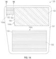
- Figure 1A illustrates a perspective, frontal view of an optical device 100.
- the optical device 100 described below is an exemplary optical device.
- the optical device 100 is a waveguide combiner, such as an augmented reality waveguide combiner.
- the optical device 100 is a flat optical device, such as a metasurface.
- the optical device 100 includes a plurality of device structures 102 disposed in (as shown in Figure 1B ) or on (as shown in Figure 1C ) a substrate 101. As shown in Figure 1C , the device structures 102 are formed in a device layer 114 formed on the substrate 101.
- the device structures 102 may be nanostructures having sub-micron dimensions, e.g., nano-sized dimensions, such as critical dimensions less than 1 ⁇ m.
- regions of the device structures 102 correspond to one or more gratings 104, such as a first grating 104a, a second grating 104b, and a third grating 104c.
- the optical device 100 is a waveguide combiner that includes at least the first grating 104a corresponding to an input coupling grating and the third grating 104c corresponding to an output coupling grating.
- the waveguide combiner according to the embodiment, which can be combined with other embodiments described herein, may include the second grating 104b corresponding to an intermediate grating.
- Figure 1B and Figure 1C are schematic, cross-sectional view of a plurality of device structures 102.
- the device structures 102 are blazed device structures 106 of a flat optical device, such as a metasurface.
- the method 400 described herein forms the blazed devices structures 106.
- the device structures 102 are blazed device structures 106 of a waveguide combiner, such as an augmented reality waveguide combiner.
- the waveguide combiner according to the embodiment, which can be combined with other embodiments described herein, may include blazed devices structures 106 in at least one of the gratings 104.
- Each of the blazed device structures 106 includes a blazed surface 108, a sidewall 112, a depth h, and a linewidth d.
- the blazed surface 108 has a plurality of steps 110. In one embodiment, which can be combined with other embodiments described herein, the blazed surface 108 includes at least 16 steps 110, such as greater than 32 steps 110, for example 64 steps 110.
- the blazed surface 108 has a blaze angle ⁇ .
- the blaze angle ⁇ is the angle between the blazed surface 108 and the surface parallel p of the substrate 101 and the angle between the surface normal of the substrate 101 and facet normal f of the blazed surface 108.
- the depth h corresponds to the height of the sidewall 112 and the linewidth d corresponds to the distances between sidewalls 112 of adjacent blazed device structures 106.
- the blaze angle ⁇ of two or more blazed devices structures 106 are different. In another embodiment, which can be combined with other embodiments described herein, the blaze angle ⁇ of two or more blazed devices structures 106 are the same. In one embodiment, which can be combined with other embodiments described herein, the depth h of two or more blazed devices structures 106 are different. In another embodiment, which can be combined with other embodiments described herein, the depth h of two or more blazed devices structures 106 are the same. In one embodiment, which can be combined with other embodiments described herein, the linewidth d of two or more blazed devices structures 106 are different. In another embodiment, which can be combined with other embodiments described herein, the linewidths d of one or more blazed devices structures 106 are the same.
- the substrate 101 may also be selected to transmit a suitable amount of light of a desired wavelength or wavelength range, such as one or more wavelengths from about 100 to about 3000 nanometers. Without limitation, in some embodiments, the substrate 101 is configured such that the substrate 101 transmits greater than or equal to about 50% to about 100% of an IR to UV region of the light spectrum.
- the substrate 101 may be formed from any suitable material, provided that the substrate 101 can adequately transmit light in a desired wavelength or wavelength range and can serve as an adequate support for the blazed devices structures 106 (when the blazed devices structures 106 are formed in the device layer 114) described herein.
- Substrate selection may include substrates of any suitable material, including, but not limited to, amorphous dielectrics, non-amorphous dielectrics, crystalline dielectrics, silicon oxide, polymers, and combinations thereof.
- the substrate 101 includes a transparent material. Suitable examples may include an oxide, sulfide, phosphide, telluride or combinations thereof.
- the substrate 101 includes silicon (Si), silicon dioxide (SiO 2 ), germanium (Ge), silicon germanium (SiGe), sapphire, and high-index transparent materials such as high-refractive-index glass.
- the device layer 114 includes, but is not limited to, one or more of silicon oxycarbide (SiOC), titanium dioxide (TiO 2 ), silicon dioxide (SiO 2 ), vanadium (IV) oxide (VOx), aluminum oxide (Al 2 O 3 ), aluminum-doped zinc oxide (AZO), indium tin oxide (ITO), tin dioxide (SnO 2 ), zinc oxide (ZnO), tantalum pentoxide (Ta 2 O 5 ), silicon nitride (Si 3 N 4 ), zirconium dioxide (ZrO 2 ), niobium oxide (Nb 2 O 5 ), cadmium stannate (Cd 2 SnO 4 ), or silicon carbon-nitride (SiCN) containing materials.
- SiOC silicon oxycarbide
- TiO 2 titanium dioxide
- SiO 2 silicon dioxide
- AZO aluminum oxide
- ITO indium tin oxide
- SnO 2 silicon dioxide
- the material of the device layer 114 may have a refractive index between about 1.5 and about 2.65. In other embodiments, which can be combined with other embodiments described herein, the material of the device layer 114 may have a refractive index between about 3.5 and about 4.0.
- Figure 2 is a schematic, side view of an angled etch system 200. It is to be understood that the angled etch system 200 described below is an exemplary angled etch system and other angled etch systems may be used with or modified to fabricate the optical devices 100 having blazed device structures 106 in accordance with the embodiments of the disclosure.
- the angled etch system 200 includes an ion beam chamber 202.
- a power source 204, a first gas source 206, and a second gas source are coupled to the ion beam chamber 202.
- the power source 204 is a radio frequency (RF) power source.
- the first gas source 206 is in fluid communication with the interior volume 205 of ion beam chamber 202.
- the first gas source 206 is an inert gas source which supplies an inert gas, such as argon, hydrogen, or helium, to the ion beam chamber 202.
- the second gas source 208 is in fluid communication with the interior volume 205 of ion beam chamber 202.
- the second gas source 208 is a process gas source which supplies a process gas to the ion beam chamber 202.
- the process gas includes, but is not limited to, one or more of a chlorine containing gas, a fluorine containing gas, a bromine containing gas, an oxygen containing gas, a silicon containing gas, nitrogen containing gas, hydrogen containing gas, or the like.
- a chlorine containing gas a fluorine containing gas
- a bromine containing gas an oxygen containing gas
- a silicon containing gas a silicon containing gas
- nitrogen containing gas nitrogen containing gas
- hydrogen containing gas hydrogen containing gas
- a first process gas may have a substrate etch chemistry that is selective to a resist material.
- the etch selectivity of the first process gas having the substrate etch chemistry provides for a selectivity of the substrate material to the resist material (described below) of about 5:1 or greater.
- the etch selectivity of the first process gas having the device material etch chemistry provides for a selectivity of the device material to a resist material of about 5:1 or greater.
- the substrate etch chemistry includes a chlorine containing gas, a fluorine containing gas, or a combination thereof.
- the device material etch chemistry includes the chlorine containing gas, the fluorine containing gas, or the combination thereof.
- a second process gas may have a resist etch chemistry that is selective to the substrate material or device material.
- the etch selectivity of the second process gas having the resist etch chemistry provides for a selectivity of the resist material to the substrate material of about 10:1 or greater or a selectivity of the resist material to the device material of about 10:1 or greater.
- the resist etch chemistry includes oxygen gas (O 2 ) and carbon tetrafluoride (CF 4 ).
- the resist etch chemistry includes argon gas (Ar), nitrogen gas (N 2 ), and hydrogen gas (H 2 ).
- the resist etch chemistry includes nitrogen gas (N 2 ) and hydrogen gas (H 2 ).
- a plasma is generated in the ion beam chamber 202 by applying RF power via the power source 204 to the inert gas and the process gas provided to the interior volume 205 of ion beam chamber 202 to generate a plasma. Ions of the plasma of the inert gas and the process gas are extracted through an aperture 210 of an extraction plate 212 to generate an ion beam 216.
- the aperture 210 of the ion beam chamber 202 is operable to direct the ion beam 216 at an angle ⁇ relative to a datum plane 218 oriented normal to the substrate 101 (i.e., the surface normal s).
- the ion beam 216 includes, but is not limited to, a spot beam, a ribbon beam, or a full substrate-size beam.
- the ion beam 216 generated includes one of the substrate etch chemistry, the device material etch chemistry, or the resist etch chemistry dependent on the process gas utilized.
- the substrate 101 is retained on a platen 214 coupled to a first actuator 219.
- the first actuator 219 which may be a linear actuator, a rotary actuator, a stepper motor, or the like, is configured to move the platen 214 in a scanning motion along a y-direction and/or a z-direction.
- the first actuator 219 is further configured to tilt the platen 214 such that the substrate 101 is positioned at a tilt angle ⁇ relative to the x-axis of the ion beam chamber 202.
- the angle ⁇ and tilt angle ⁇ result in a beam angle ⁇ relative to the datum plane 218 normal to the substrate 101.
- a second actuator 220 may also be coupled to the platen 214 to rotate the substrate 101 about the x-axis of the platen 214.
- Figure 3 is a schematic, cross-sectional view of angled etch system 300. It is to be understood that the angled etch system 300 described below is an exemplary angled etch system and other angled etch systems may be used with or modified to fabricate the optical devices 100 having blazed device structures 106 in accordance with the embodiments of the disclosure.
- the angled etch system 300 includes an electron beam chamber 302.
- a power source 304, a first gas source 306, and a second gas source 308 are coupled to the electron beam chamber 302.
- the first gas source 306 and the second gas source 308 are in fluid communication with the interior volume 305 of electron beam chamber 302.
- the first gas source 306 and the second gas source 308 may extend through the electrode 322 or the electrode 322 may include a plurality of apertures to function as a gas delivery showerhead.
- the first gas source 306 is an inert gas source which supplies the inert gas (as described above) to the electron beam chamber 302.
- the second gas source 308 is a process gas source (as described above) which supplies a process gas to the ion beam chamber 202.
- two or more process gases may be utilized.
- the two or more process gases include the substrate etch chemistry, the device material etch chemistry, and the resist etch chemistry described herein.
- the substrate 101 is retained on a platen 314 coupled to a first actuator 321.
- the first actuator 321 which may be a linear actuator, a rotary actuator, a stepper motor, or the like, is configured to raise and lower the platen 314 within the electron beam chamber 302.
- a second actuator 320 may also be coupled to the platen 314 to rotate the substrate 101 about a vertical axis of the platen 314.
- the platen 314 includes an electrode 324 disposed therein.
- the electrode 324 is a chucking apparatus, such as an electrostatic chuck, for securing a substrate 101 thereto during processing of the substrate 101. Power from the power source 304 may be utilized to bias the electrode 324 to either chuck the substrate 101 to the electrode 324 or influence bombardment of electrons on the substrate 101.
- a plasma is generated in the electron beam chamber 302 by various bulk and surface processes, for example, by inductive coupling. It is believed that ions generated by an inductively coupled plasma are influenced by an electric field that encourages bombardment of the electrode 322 by the ions generated from the plasma of the inert gas and the process gas.
- Other plasma generation processes such as a capacitively coupled arrangement, hollow cathode arrangement, direct current electrode biasing, or electron beam plasma generation processes may be utilized in accordance with the embodiments described herein.
- Ion bombardment of the electrode 322 is believed to cause the electrode 322 to emit secondary electrons.
- Energetic secondary electrons which have a negative charge, are emitted from the electrode 322.
- an electron beam 316 is accelerated from the electrode 322 at beam angle ⁇ relative to a datum plane 318 oriented normal to the substrate 101 (i.e., the surface normal s).
- the electron beam 316 includes, but is not limited to, a spot beam, a ribbon beam, or a full substrate-size beam.
- the electron beam 316 generated includes one of the substrate etch chemistry, the device material etch chemistry, or the resist etch chemistry dependent on the process gas utilized.
- the ion beam 216 generated from the angled etch system 200 (e.g., an ion beam etch system) and electron beam 316 generated from the angled etch system 300 (e.g., an electron beam etch system) are collectively described as a beam 516 (as shown in Figures 5A-5J ) where the beam 516 is one of an ion beam or an electron beam.
- the beam 516 has one of the substrate etch chemistry, the device material etch chemistry, or the resist etch chemistry at operations of the method 400 described herein.
- At least the substrate etch chemistry and resist etch chemistry are different. In other embodiments, which may be combined with other embodiments described herein, at least the device material etch chemistry and resist etch chemistry are different. As described herein, the tunability of etch rates of the resist material 506 and one of a device layer 114 or the substrate 101 and rotation of the substrate 101 form the blazed optical device structures without multiple lithographic patterning steps and angled etch steps.
- Figure 4 is a flow diagram of a method 400 for forming a plurality of blazed device structures 106 of an optical device structure 100 as shown in Figures 5A-5E and 5F-5J .
- Figures 5A-5E are schematic, cross sectional views of a portion 501 of a substrate 101 during the method 400.
- Figures 5F-5J are schematic, top views of the portion 501 of the substrate 101 during the method 400.
- the method 400 will be described with reference to the angled etch system 200 of Figure 2 and the angled etch system 300 of Figure 3 .
- angled etch systems other than the angled etch systems 200, 300 may be utilized in conjunction with method 400.
- the portion 501 may correspond to a portion or a whole surface of the substrate 101 of a flat optical device to have the plurality of blazed device structures 106 formed thereon.
- the portion 501 may correspond to a portion or a whole surface of the substrate 101 of a waveguide combiner to have the plurality of blazed device structures 106 formed thereon.
- the portion 501 may correspond to one or more gratings 104. While Figures 5A-5E and Figures 5F-5J depict etching the substrate 101 such that the blazed device structures 106 are disposed in the substrate, a device layer 114 (as described above) may be disposed on the surface 103 such that the blazed device structures 106 are disposed in the device layer 114.
- a substrate 101 is positioned at a first rotation angle ⁇ 1 as defined by datum line 502, as shown in Figures 5F .
- the first rotation angle ⁇ 1 is 0° defined by datum line 502.
- the substrate 101 or the device layer 114 includes a patterned resist 504 disposed thereon.
- the pattern resist 504 includes a resist material 506 that is patterned into a plurality of resist structures 508 disposed over a surface 103 of substrate 101.
- the resist material 506 of the patterned resist 504 is selected based on the substrate etch chemistry (in embodiments in which the substrate 101 is etched to form the blazed device structures 106) or the device material etch chemistry (in embodiments in which the device layer 114 is etched to form the blazed device structures 106).
- the resist material 506 is a photosensitive material such that the patterned resist 504 may be patterned by a lithography process, such as photolithography or digital lithography, or by laser ablation process to form the plurality of resist structures 508.
- the resist material 506 is an imprintable material that the patterned resist 504 may be patterned by a nanoimprint process to form the plurality of resist structures 508.
- the resist material 506 is a hardmask material and the patterned resist 504 is a patterned via one or more etch processes to form the plurality of resist structures 508.
- the patterned resist 504 is an optical planarization layer.
- Each resist structure 508 includes a bottom surface 509, a first sidewall 510, a second sidewall 512, and a top surface 514. Each resist structure 508 has a height 515 from the bottom surface 509 to the top surface 514. Each resist structure 508 has a width 522 from the first sidewall 510 to the second sidewall 512 of the resist structure 508. A plurality of gaps 518 are defined by adjacent resist structures 508. Each of the gaps 518 has a linewidth 520 between the first sidewall 510 and the second sidewall 512 of adjacent resist structures 508.
- the height 515, the linewidth 520, and the width 522 are selected to tune the number of steps 110 of blazed surface 108 and the linewidth d of the plurality of blazed device structures 106. For example, increasing the height 515 increases the number of repeated intervals of etching the substrate 101 (or device layer 114) and the resist structure 508 such that the number of steps 110 is increased.
- the substrate 101 is exposed to the beam 516 at the beam angle ⁇ relative to the surface normal of the substrate 101.
- the beam angle ⁇ is about 10 degrees to about 80 degrees relative to the surface normal of the substrate 101.
- the beam 516 has the substrate etch chemistry or device etch chemistry that is selective to the resist material 506, i.e., exposed portions 517 of the substrate 101 or exposed portions of the device layer 114 (not shown) are removed at a higher rate than the resist material 506.
- the depth h of the exposed portions 517 corresponding to the blazed device structures 106 is formed.
- substrate 101 is rotated to a second rotation angle ⁇ 2 defined by datum line 502, as shown in Figures 5H .
- the platen 214, 314 retaining substrate 101 is rotated to a second rotation angle ⁇ 2 .
- the second rotation angle ⁇ 2 corresponds to 90° relative to datum line 502.
- the rotating of the substrate 101 is not limited to a rotation angle ⁇ corresponding to 90° but may correspond to any predetermined angle ⁇ . The rotation enables the beam 516 to contact resist structures 508 due to a shadowing effect.
- the beam 516 will remain at a beam angle ⁇ relative to a datum plane 218, 318 oriented normal to the substrate 101 (i.e., the surface normal s) throughout method 400.
- the constant beam angle allows for the throughput to increase because there will not be a need to reconfigure the beam angle ⁇ .
- the method 400 described herein uses only one angled etch system 200, 300 and requires the resist material 506 to only be patterned once to provide for high volume production capability.
- the resist structures are exposed to the beam 516 at the beam angle ⁇ .
- the beam 516 etches one of either the first sidewall 510 or the second sidewall 512, corresponding to which sidewall 510, 512 is exposed to the beam 516.
- the first sidewall 510 is exposed to the beam 516.
- the beam 516 has a chemistry corresponding to the resist etch chemistry so that the ions or electrons will only substantially etch the resist structures 508 during the resist etch process.
- the resist etch chemistry is selective to the substrate 101 or device layer 114, i.e., the resist structures 508 are removed at a higher rate than the device layer 114 or substrate 101.
- the width 522 of resist structure 508 decreases relative to the width shown in Figures 5A and 5B .
- the linewidth 520 between the first sidewall and the second sidewall increases relative to the linewidth shown in Figures 5A and 5B .
- a first step of the plurality of steps 110 is formed.
- the plurality of steps 110 forms the blazed surface 108 shown in Figures 1B and 1C .
- the blaze angle ⁇ is the angle between the blazed surface 108 and the surface parallel p of the substrate 101.
- the blaze angle ⁇ may be achieved by increasing or decreasing the etch rate of beam 516.
- the adjustments of blaze angle ⁇ may be accomplished by etching at different rates such that depth h, linewidth 520 and width 522 are at predetermined values corresponding to a different number of steps 110 formed on blazed surface 108.
- the blaze angle ⁇ may be adjusted and the blazed device structures 106, such as the blazed device structures 106 of a grating 104, may modulate light propagating through the optical device 100 as desired.
- operations 401-404 are repeated until a predetermined number of steps 110 (as shown in Figures 1B and 1C ) are formed on optical device 100.
- the substrate 101 is rotated to the first rotation angle ⁇ 1 and substrate 101 or device layer 114 are etched with the beam 516 until the resist structures 508 are removed or the linewidth 520 of the gaps 518 has a predetermined linewidth.
- the platen 214, 314 with substrate 101 positioned thereon is rotated to a first rotation angle ⁇ 1 .
- the depth h of the exposed portions 517 corresponding to the blazed device structures 106 increases relative to the depth h shown in Figures 5A-5C .
- the platen 214, 314 with substrate 101 positioned thereon is rotated to a second rotation angle ⁇ 2 defined by datum line 502.
- the width 522 of resist structure 508 decreases relative to the width shown in Figures 5A-5D .
- the linewidth 520 between the first sidewall 510 and the second sidewall 512 increases relative to the linewidth 520 shown in Figures 5A-5D .
- residual resist material 506 disposed on the device layer 114 or substrate 101 is removed. While only four resist structures 508 and three gaps 518 are illustrated, the entire patterned resist 504 may be etched such that the desired number of blazed device structures 106 are formed depending on the predetermined design for the optical device 100.
- optical device structures are described herein.
- the methods utilize rotation of a substrate, to have the blazed optical device structures formed thereon, and tunability of etch rates of a patterned resist disposed over the substrate and one of a device layer or the substrate to form the blazed optical device structures without multiple lithographic patterning steps and angled etch steps.
- the constant beam angle allows for the throughput to increase because there will not be a need reconfigure the beam angle ⁇ . Only one angled etch system may be used and the resist material would only need to be patterned once to provide for high volume production capability.
Landscapes
- Physics & Mathematics (AREA)
- General Physics & Mathematics (AREA)
- Optics & Photonics (AREA)
- Engineering & Computer Science (AREA)
- Manufacturing & Machinery (AREA)
- Diffracting Gratings Or Hologram Optical Elements (AREA)
- Drying Of Semiconductors (AREA)
- Optical Integrated Circuits (AREA)
- Optical Couplings Of Light Guides (AREA)
Abstract
Description
- Embodiments of the present invention generally relate to optical devices for augmented, virtual, and mixed reality. More specifically, embodiments described herein provide for forming blazed optical device structures.
- Virtual reality is generally considered to be a computer generated simulated environment in which a user has an apparent physical presence. A virtual reality experience can be generated in 3D and viewed with a head-mounted display (HMD), such as glasses or other wearable display devices that have near-eye display panels as lenses to display a virtual reality environment that replaces an actual environment.
- Augmented reality, however, enables an experience in which a user can still see through the display lenses of the glasses or other HMD device to view the surrounding environment, yet also see images of virtual objects that are generated for display and appear as part of the environment. Augmented reality can include any type of input, such as audio and haptic inputs, as well as virtual images, graphics, and video that enhances or augments the environment that the user experiences. As an emerging technology, there are many challenges and design constraints with augmented reality.
- One such challenge is displaying a virtual image overlaid on an ambient environment. Optical devices including waveguide combiners, such as augmented reality waveguide combiners, and flat optical devices, such as metasurfaces, are used to assist in overlaying images. Generated light is propagated through an optical device until the light exits the optical device and is overlaid on the ambient environment. Optical devices may require structures having blazed angles relative to the surface of the optical device substrate. Conventionally, fabricating blazed optical device structures using one or more angled etch tools requires multiple lithographic patterning steps and angled etch steps. The multiple lithographic patterning steps and angled etch steps increase fabrication time and increase cost.
- Accordingly, what is needed in the art are improved methods of forming optical devices including blazed optical device structures with angled etch tools.
- In one embodiment, an augmented reality waveguide combiner is provided. The waveguide combiner includes a substrate and a grating disposed in or on a surface of the substrate. The grating has a plurality of blazed device structures. Each blazed device structure of the plurality of blazed device includes a blazed surface. The blazed surface has at least 16 steps, a facet normal of each of the steps parallel to the surface of the substrate, and a blaze angle defined by the blazed surface and the facet normal.
- The blaze angle of two blazed device structures of the plurality of blazed device structures may be different. The blaze angle of two blazed device structures of the plurality of blazed device structures may be the same. The two blazed device structures of the plurality of blazed device structures may have different depths. A device layer including the grating may include one or more of silicon oxycarbide (SiOC), titanium dioxide (TiO2), silicon dioxide (SiO2), vanadium (IV) oxide (VOx), aluminum oxide (Al2O3), aluminum-doped zinc oxide (AZO), indium tin oxide (ITO), tin dioxide (SnO2), zinc oxide (ZnO), tantalum pentoxide (Ta2O5), silicon nitride (Si3N4), zirconium dioxide (ZrO2), niobium oxide (Nb2O5), cadmium stannate (Cd2SnO4), or silicon carbon-nitride (SiCN) containing materials. The substrate may include non-amorphous dielectrics, crystalline dielectrics, silicon oxide, polymers, or combinations thereof. The substrate may include silicon (Si), silicon dioxide (SiO2), germanium (Ge), silicon germanium (SiGe), sapphire, or combinations thereof.
- In one example, a method is provided. The method includes positioning a substrate at a first rotation angle φ1 in the path of a beam. The beam is configured to be projected to a surface of the substrate at a beam angle ϑ relative to a surface normal of the substrate. A patterned resist is formed over the substrate where the patterned resist includes two or more resist structures and one or more gaps. Each of the resist structures has a width and each of the gaps is defined by adjacent resist structures and has a linewidth defined by the adjacent resist structures. The method includes etching the substrate positioned at the first rotation angle φ1 with the beam and rotating the substrate to a second rotation angle φ2 and etching sidewalls of the resist structures oriented toward the beam such that the width of the resist structures decreases and the linewidth of the gaps increases. The method further includes rotating the substrate to the first rotation angle φ1 and etching the substrate at the first rotation angle φ1 with the beam and forming two or more optical device structures in the substrate. The forming the optical device structures includes repeating the rotating the substrate to the second rotation angle φ2 and the etching sidewalls of the resist structures with the beam and the rotating the substrate to the first rotation angle φ2 and the etching the substrate with the beam until the resist structures are removed or the linewidth of the gaps has a predetermined linewidth.
- In another example, a method is provided. The method includes positioning a substrate at a first rotation angle φ1 in the path of a beam. The beam is configured to be projected to a surface of the substrate at a beam angle ϑ relative to a surface normal of the substrate. A device layer is formed over the substrate and a patterned resist is formed on the device layer. The patterned resist includes two or more resist structures and one or more gaps. Each of the resist structures has a width and each of the gaps is defined by adjacent resist structures and has a linewidth defined by the adjacent resist structures. The method includes etching the device layer with the substrate positioned at the first rotation angle φ1 with the beam and rotating the substrate to a second rotation angle φ2 and etching sidewalls of the resist structures oriented toward the beam such that the width of the resist structures decreases and the linewidth of the gaps increases. The method further includes rotating the substrate to the first rotation angle φ1 and etching the device layer at the first rotation angle φ1 with the beam and forming two or more optical device structures in the device layer. The forming the optical device structures includes repeating the rotating the substrate to the second rotation angle φ2 and the etching sidewalls of the resist structures with the beam and the rotating the substrate to the first rotation angle φ2 and the etching the device layer with the beam until the resist structures are removed or the linewidth of the gaps has a predetermined linewidth.
- In yet another example, a method is provided. The method includes positioning a substrate at a first rotation angle φ1 in the path of a beam. The beam is configured to be projected to a surface of the substrate at a beam angle ϑ relative to a surface normal of the substrate. A patterned resist is formed over the substrate where the patterned resist includes two or more resist structures and one or more gaps. Each of the resist structures has a width and each of the gaps is defined by adjacent resist structures and has a linewidth defined by the adjacent resist structures. The substrate is etched by the beam generated by a substrate etch chemistry and the resist structures are etched by the beam generated by a resist etch chemistry different than the substrate etch chemistry. The method further includes etching the substrate positioned at the first rotation angle φ1 with the beam generated by the substrate etch chemistry and rotating the substrate to a second rotation angle φ2 and etching sidewalls of the resist structures with the beam at the beam angle ϑ. The beam generated by the resist etch chemistry etches sidewalls of resist structures oriented toward the beam such that the width of the resist structures decreases and the linewidth of the gaps increases. The method further includes rotating the substrate to the first rotation angle φ1 and etching the substrate at the first rotation angle φ1 with the beam generated by the substrate etch chemistry and forming two or more optical device structures in the substrate. The forming the optical device structures comprises repeating the rotating the substrate to the second rotation angle φ2 and the etching sidewalls of the resist structures with the beam generated by the resist etch chemistry and rotating the substrate to the first rotation angle φ1 and the etching the substrate with the beam generated by the substrate etch chemistry until the resist structures are removed or the linewidth of the gaps has a predetermined linewidth.
- So that the manner in which the above recited features of the present disclosure can be understood in detail, a more particular description of the disclosure, briefly summarized above, may be had by reference to embodiments, some of which are illustrated in the appended drawings. It is to be noted, however, that the appended drawings illustrate only exemplary embodiments and are therefore not to be considered limiting of its scope, and may admit to other equally effective embodiments.
-
Figure 1A is a perspective, frontal view of an optical device according to embodiments described herein. -
Figure 1B andFigure 1C are schematic, cross-sectional views of a plurality of device structures according to embodiments described herein. -
Figure 2 is a schematic, side view of an angled etch system according to embodiments described herein. -
Figure 3 is a schematic cross-sectional view of angled etch system according to embodiments described herein. -
Figure 4 is a flow diagram of a method for forming a plurality of blazed device structures of an optical device structure according to embodiments described herein. -
Figures 5A-5E are schematic, cross sectional views of a portion of a substrate during a method for forming a plurality of blazed device structures according to embodiments described herein. -
Figures 5F-5J are schematic, top views of a portion of a substrate during a method for forming a plurality of blazed device structures according to embodiments described herein. - To facilitate understanding, identical reference numerals have been used, where possible, to designate identical elements that are common to the figures. It is contemplated that elements and features of one embodiment may be beneficially incorporated in other embodiments without further recitation.
- Embodiments of the present invention generally relate to optical devices for augmented, virtual, and mixed reality. More specifically, embodiments described herein provide for methods of forming optical device structures. The methods utilize rotation of a substrate, to have the optical device structures formed thereon, and tunability of etch rates of a patterned resist disposed over the substrate and one of a device layer or the substrate to form the optical device structures without multiple lithographic patterning steps and angled etch steps.
- In one embodiment, the method includes positioning a substrate at a first rotation angle φ1 in a path of a beam, the beam configured to be projected to a surface of the substrate at a beam angle ϑ relative to a surface normal of the substrate. The substrate has a patterned resist formed thereover. The patterned resist includes two or more resist structures. Each of the resist structures has a width and one or more gaps. Each of the gaps is defined by adjacent resist structures and having a linewidth defined by the adjacent resist structures. The substrate positioned at the first rotation angle φ1 is etched with the beam. The substrate is rotated to a second rotation angle φ2 and sidewalls of the resist structures are etched with the beam at the beam angle ϑ such that the width of the resist structures decreases and the linewidth of the gaps increases. The substrate is rotated to the first rotation angle φ1 and the substrate is etched at the first rotation angle φ1 with the beam. Two or more optical device structures are formed in the substrate. The forming the optical device structures includes repeating the rotating the substrate to the second rotation angle φ2 and the etching sidewalls of the resist structures with the beam, and the rotating the substrate to the first rotation angle φ1 and the etching the substrate with the beam until the resist structures are removed or the linewidth of the gaps has a predetermined linewidth.
-
Figure 1A illustrates a perspective, frontal view of anoptical device 100. It is to be understood that theoptical device 100 described below is an exemplary optical device. In one embodiment, which can be combined with other embodiments described herein, theoptical device 100 is a waveguide combiner, such as an augmented reality waveguide combiner. In another embodiment, which can be combined with other embodiments described herein, theoptical device 100 is a flat optical device, such as a metasurface. Theoptical device 100 includes a plurality ofdevice structures 102 disposed in (as shown inFigure 1B ) or on (as shown inFigure 1C ) asubstrate 101. As shown inFigure 1C , thedevice structures 102 are formed in adevice layer 114 formed on thesubstrate 101. Thedevice structures 102 may be nanostructures having sub-micron dimensions, e.g., nano-sized dimensions, such as critical dimensions less than 1 µm. In one embodiment, which can be combined with other embodiments described herein, regions of thedevice structures 102 correspond to one ormore gratings 104, such as a first grating 104a, asecond grating 104b, and athird grating 104c. In one embodiment, which can be combined with other embodiments described herein, theoptical device 100 is a waveguide combiner that includes at least the first grating 104a corresponding to an input coupling grating and thethird grating 104c corresponding to an output coupling grating. The waveguide combiner according to the embodiment, which can be combined with other embodiments described herein, may include thesecond grating 104b corresponding to an intermediate grating. -
Figure 1B andFigure 1C are schematic, cross-sectional view of a plurality ofdevice structures 102. In one embodiment, which can be combined with other embodiments described herein, thedevice structures 102 are blazeddevice structures 106 of a flat optical device, such as a metasurface. Themethod 400 described herein forms the blazeddevices structures 106. In another embodiment, which can be combined with other embodiments described herein, thedevice structures 102 are blazeddevice structures 106 of a waveguide combiner, such as an augmented reality waveguide combiner. The waveguide combiner according to the embodiment, which can be combined with other embodiments described herein, may include blazeddevices structures 106 in at least one of thegratings 104. Each of the blazeddevice structures 106 includes a blazedsurface 108, asidewall 112, a depth h, and a linewidth d. The blazedsurface 108 has a plurality ofsteps 110. In one embodiment, which can be combined with other embodiments described herein, the blazedsurface 108 includes at least 16steps 110, such as greater than 32steps 110, for example 64steps 110. The blazedsurface 108 has a blaze angle γ. The blaze angle γ is the angle between the blazedsurface 108 and the surface parallel p of thesubstrate 101 and the angle between the surface normal of thesubstrate 101 and facet normal f of the blazedsurface 108. The depth h corresponds to the height of thesidewall 112 and the linewidth d corresponds to the distances betweensidewalls 112 of adjacent blazeddevice structures 106. - In one embodiment, which can be combined with other embodiments described herein, the blaze angle γ of two or more blazed
devices structures 106 are different. In another embodiment, which can be combined with other embodiments described herein, the blaze angle γ of two or more blazeddevices structures 106 are the same. In one embodiment, which can be combined with other embodiments described herein, the depth h of two or more blazeddevices structures 106 are different. In another embodiment, which can be combined with other embodiments described herein, the depth h of two or more blazeddevices structures 106 are the same. In one embodiment, which can be combined with other embodiments described herein, the linewidth d of two or more blazeddevices structures 106 are different. In another embodiment, which can be combined with other embodiments described herein, the linewidths d of one or more blazeddevices structures 106 are the same. - The
substrate 101 may also be selected to transmit a suitable amount of light of a desired wavelength or wavelength range, such as one or more wavelengths from about 100 to about 3000 nanometers. Without limitation, in some embodiments, thesubstrate 101 is configured such that thesubstrate 101 transmits greater than or equal to about 50% to about 100% of an IR to UV region of the light spectrum. Thesubstrate 101 may be formed from any suitable material, provided that thesubstrate 101 can adequately transmit light in a desired wavelength or wavelength range and can serve as an adequate support for the blazed devices structures 106 (when the blazeddevices structures 106 are formed in the device layer 114) described herein. Substrate selection may include substrates of any suitable material, including, but not limited to, amorphous dielectrics, non-amorphous dielectrics, crystalline dielectrics, silicon oxide, polymers, and combinations thereof. In some embodiments, which can be combined with other embodiments described herein, thesubstrate 101 includes a transparent material. Suitable examples may include an oxide, sulfide, phosphide, telluride or combinations thereof. In one example, thesubstrate 101 includes silicon (Si), silicon dioxide (SiO2), germanium (Ge), silicon germanium (SiGe), sapphire, and high-index transparent materials such as high-refractive-index glass. - In some embodiments, which can be combined with other embodiments described herein, the
device layer 114 includes, but is not limited to, one or more of silicon oxycarbide (SiOC), titanium dioxide (TiO2), silicon dioxide (SiO2), vanadium (IV) oxide (VOx), aluminum oxide (Al2O3), aluminum-doped zinc oxide (AZO), indium tin oxide (ITO), tin dioxide (SnO2), zinc oxide (ZnO), tantalum pentoxide (Ta2O5), silicon nitride (Si3N4), zirconium dioxide (ZrO2), niobium oxide (Nb2O5), cadmium stannate (Cd2SnO4), or silicon carbon-nitride (SiCN) containing materials. In some embodiments, which can be combined with other embodiments described herein, the material of thedevice layer 114 may have a refractive index between about 1.5 and about 2.65. In other embodiments, which can be combined with other embodiments described herein, the material of thedevice layer 114 may have a refractive index between about 3.5 and about 4.0. -
Figure 2 is a schematic, side view of anangled etch system 200. It is to be understood that theangled etch system 200 described below is an exemplary angled etch system and other angled etch systems may be used with or modified to fabricate theoptical devices 100 having blazeddevice structures 106 in accordance with the embodiments of the disclosure. - The
angled etch system 200 includes anion beam chamber 202. Apower source 204, afirst gas source 206, and a second gas source are coupled to theion beam chamber 202. In one embodiment, which can be combined with other embodiments described herein, thepower source 204 is a radio frequency (RF) power source. Thefirst gas source 206 is in fluid communication with theinterior volume 205 ofion beam chamber 202. Thefirst gas source 206 is an inert gas source which supplies an inert gas, such as argon, hydrogen, or helium, to theion beam chamber 202. Thesecond gas source 208 is in fluid communication with theinterior volume 205 ofion beam chamber 202. Thesecond gas source 208 is a process gas source which supplies a process gas to theion beam chamber 202. The process gas includes, but is not limited to, one or more of a chlorine containing gas, a fluorine containing gas, a bromine containing gas, an oxygen containing gas, a silicon containing gas, nitrogen containing gas, hydrogen containing gas, or the like. In the embodiments of themethod 400 described herein, which can be combined with other embodiments described herein, two or more process gases may be utilized. - A first process gas may have a substrate etch chemistry that is selective to a resist material. The etch selectivity of the first process gas having the substrate etch chemistry provides for a selectivity of the substrate material to the resist material (described below) of about 5:1 or greater. The etch selectivity of the first process gas having the device material etch chemistry provides for a selectivity of the device material to a resist material of about 5:1 or greater. In one embodiment, which can be combined with other embodiments described herein, the substrate etch chemistry includes a chlorine containing gas, a fluorine containing gas, or a combination thereof. In another embodiment, which can be combined with other embodiments described herein, the device material etch chemistry includes the chlorine containing gas, the fluorine containing gas, or the combination thereof.
- A second process gas may have a resist etch chemistry that is selective to the substrate material or device material. The etch selectivity of the second process gas having the resist etch chemistry provides for a selectivity of the resist material to the substrate material of about 10:1 or greater or a selectivity of the resist material to the device material of about 10:1 or greater. In one embodiment, which can be combined with other embodiments described herein, the resist etch chemistry includes oxygen gas (O2) and carbon tetrafluoride (CF4). In another embodiment, which can be combined with other embodiments described herein, the resist etch chemistry includes argon gas (Ar), nitrogen gas (N2), and hydrogen gas (H2). In yet another embodiment, which can be combined with other embodiments described herein, the resist etch chemistry includes nitrogen gas (N2) and hydrogen gas (H2).
- In operation, a plasma is generated in the
ion beam chamber 202 by applying RF power via thepower source 204 to the inert gas and the process gas provided to theinterior volume 205 ofion beam chamber 202 to generate a plasma. Ions of the plasma of the inert gas and the process gas are extracted through anaperture 210 of anextraction plate 212 to generate anion beam 216. Theaperture 210 of theion beam chamber 202 is operable to direct theion beam 216 at an angle α relative to adatum plane 218 oriented normal to the substrate 101 (i.e., the surface normal s). Theion beam 216 includes, but is not limited to, a spot beam, a ribbon beam, or a full substrate-size beam. Theion beam 216 generated includes one of the substrate etch chemistry, the device material etch chemistry, or the resist etch chemistry dependent on the process gas utilized. - The
substrate 101 is retained on aplaten 214 coupled to afirst actuator 219. Thefirst actuator 219, which may be a linear actuator, a rotary actuator, a stepper motor, or the like, is configured to move theplaten 214 in a scanning motion along a y-direction and/or a z-direction. In one embodiment, which can be combined with other embodiments described herein, thefirst actuator 219 is further configured to tilt theplaten 214 such that thesubstrate 101 is positioned at a tilt angle β relative to the x-axis of theion beam chamber 202. The angle α and tilt angle β result in a beam angle ϑ relative to thedatum plane 218 normal to thesubstrate 101. Asecond actuator 220 may also be coupled to theplaten 214 to rotate thesubstrate 101 about the x-axis of theplaten 214. -
Figure 3 is a schematic, cross-sectional view ofangled etch system 300. It is to be understood that theangled etch system 300 described below is an exemplary angled etch system and other angled etch systems may be used with or modified to fabricate theoptical devices 100 having blazeddevice structures 106 in accordance with the embodiments of the disclosure. - The
angled etch system 300 includes anelectron beam chamber 302. Apower source 304, a first gas source 306, and a second gas source 308 are coupled to theelectron beam chamber 302. The first gas source 306 and the second gas source 308 are in fluid communication with theinterior volume 305 ofelectron beam chamber 302. For example, the first gas source 306 and the second gas source 308 may extend through theelectrode 322 or theelectrode 322 may include a plurality of apertures to function as a gas delivery showerhead. The first gas source 306 is an inert gas source which supplies the inert gas (as described above) to theelectron beam chamber 302. The second gas source 308 is a process gas source (as described above) which supplies a process gas to theion beam chamber 202. In the embodiments of themethod 400 described herein, which can be combined with other embodiments described herein, two or more process gases may be utilized. The two or more process gases include the substrate etch chemistry, the device material etch chemistry, and the resist etch chemistry described herein. - The
substrate 101 is retained on aplaten 314 coupled to a first actuator 321. The first actuator 321, which may be a linear actuator, a rotary actuator, a stepper motor, or the like, is configured to raise and lower theplaten 314 within theelectron beam chamber 302. Asecond actuator 320 may also be coupled to theplaten 314 to rotate thesubstrate 101 about a vertical axis of theplaten 314. Theplaten 314 includes anelectrode 324 disposed therein. In one embodiment, theelectrode 324 is a chucking apparatus, such as an electrostatic chuck, for securing asubstrate 101 thereto during processing of thesubstrate 101. Power from thepower source 304 may be utilized to bias theelectrode 324 to either chuck thesubstrate 101 to theelectrode 324 or influence bombardment of electrons on thesubstrate 101. - In operation, a plasma is generated in the
electron beam chamber 302 by various bulk and surface processes, for example, by inductive coupling. It is believed that ions generated by an inductively coupled plasma are influenced by an electric field that encourages bombardment of theelectrode 322 by the ions generated from the plasma of the inert gas and the process gas. Other plasma generation processes, such as a capacitively coupled arrangement, hollow cathode arrangement, direct current electrode biasing, or electron beam plasma generation processes may be utilized in accordance with the embodiments described herein. - Ion bombardment of the
electrode 322 is believed to cause theelectrode 322 to emit secondary electrons. Energetic secondary electrons, which have a negative charge, are emitted from theelectrode 322. As such, anelectron beam 316 is accelerated from theelectrode 322 at beam angle ϑ relative to adatum plane 318 oriented normal to the substrate 101 (i.e., the surface normal s). Theelectron beam 316 includes, but is not limited to, a spot beam, a ribbon beam, or a full substrate-size beam. Theelectron beam 316 generated includes one of the substrate etch chemistry, the device material etch chemistry, or the resist etch chemistry dependent on the process gas utilized. - As described herein, the
ion beam 216 generated from the angled etch system 200 (e.g., an ion beam etch system) andelectron beam 316 generated from the angled etch system 300 (e.g., an electron beam etch system) are collectively described as a beam 516 (as shown inFigures 5A-5J ) where thebeam 516 is one of an ion beam or an electron beam. In embodiments of themethod 400, which can be combined with other embodiments described, thebeam 516 has one of the substrate etch chemistry, the device material etch chemistry, or the resist etch chemistry at operations of themethod 400 described herein. In some embodiments, which may be combined with other embodiments described herein, at least the substrate etch chemistry and resist etch chemistry are different. In other embodiments, which may be combined with other embodiments described herein, at least the device material etch chemistry and resist etch chemistry are different. As described herein, the tunability of etch rates of the resistmaterial 506 and one of adevice layer 114 or thesubstrate 101 and rotation of thesubstrate 101 form the blazed optical device structures without multiple lithographic patterning steps and angled etch steps. -
Figure 4 is a flow diagram of amethod 400 for forming a plurality of blazeddevice structures 106 of anoptical device structure 100 as shown inFigures 5A-5E and5F-5J .Figures 5A-5E are schematic, cross sectional views of aportion 501 of asubstrate 101 during themethod 400.Figures 5F-5J are schematic, top views of theportion 501 of thesubstrate 101 during themethod 400. - To facilitate explanation, the
method 400 will be described with reference to theangled etch system 200 ofFigure 2 and theangled etch system 300 ofFigure 3 . However, it is to be noted that angled etch systems other than theangled etch systems method 400. In one embodiment, which can be combined with other embodiments described herein, theportion 501 may correspond to a portion or a whole surface of thesubstrate 101 of a flat optical device to have the plurality of blazeddevice structures 106 formed thereon. In another embodiment, which can be combined with other embodiments described herein, theportion 501 may correspond to a portion or a whole surface of thesubstrate 101 of a waveguide combiner to have the plurality of blazeddevice structures 106 formed thereon. Theportion 501 may correspond to one ormore gratings 104. WhileFigures 5A-5E andFigures 5F-5J depict etching thesubstrate 101 such that the blazeddevice structures 106 are disposed in the substrate, a device layer 114 (as described above) may be disposed on thesurface 103 such that the blazeddevice structures 106 are disposed in thedevice layer 114. - At
operation 401, as shown inFigure 5A and5F , asubstrate 101 is positioned at a first rotation angle φ1 as defined bydatum line 502, as shown inFigures 5F . In one embodiment, which may be combined with other embodiments described herein, the first rotation angle φ1 is 0° defined bydatum line 502. Thesubstrate 101 or the device layer 114 (not shown) includes a patterned resist 504 disposed thereon. The pattern resist 504 includes a resistmaterial 506 that is patterned into a plurality of resiststructures 508 disposed over asurface 103 ofsubstrate 101. The resistmaterial 506 of the patterned resist 504 is selected based on the substrate etch chemistry (in embodiments in which thesubstrate 101 is etched to form the blazed device structures 106) or the device material etch chemistry (in embodiments in which thedevice layer 114 is etched to form the blazed device structures 106). In one embodiment, the resistmaterial 506 is a photosensitive material such that the patterned resist 504 may be patterned by a lithography process, such as photolithography or digital lithography, or by laser ablation process to form the plurality of resiststructures 508. In one embodiment, the resistmaterial 506 is an imprintable material that the patterned resist 504 may be patterned by a nanoimprint process to form the plurality of resiststructures 508. In another embodiment, which may be combined with other embodiments described herein, the resistmaterial 506 is a hardmask material and the patterned resist 504 is a patterned via one or more etch processes to form the plurality of resiststructures 508. In yet another embodiment, which may be combined with other embodiments described herein, the patterned resist 504 is an optical planarization layer. - Each resist
structure 508 includes abottom surface 509, afirst sidewall 510, asecond sidewall 512, and atop surface 514. Each resiststructure 508 has aheight 515 from thebottom surface 509 to thetop surface 514. Each resiststructure 508 has awidth 522 from thefirst sidewall 510 to thesecond sidewall 512 of the resiststructure 508. A plurality ofgaps 518 are defined by adjacent resiststructures 508. Each of thegaps 518 has alinewidth 520 between thefirst sidewall 510 and thesecond sidewall 512 of adjacent resiststructures 508. Theheight 515, thelinewidth 520, and thewidth 522 are selected to tune the number ofsteps 110 of blazedsurface 108 and the linewidth d of the plurality of blazeddevice structures 106. For example, increasing theheight 515 increases the number of repeated intervals of etching the substrate 101 (or device layer 114) and the resiststructure 508 such that the number ofsteps 110 is increased. - At
operation 402, thesubstrate 101 is exposed to thebeam 516 at the beam angle ϑ relative to the surface normal of thesubstrate 101. In one embodiment, which can be combined with other embodiments described herein, the beam angle ϑ is about 10 degrees to about 80 degrees relative to the surface normal of thesubstrate 101. Thebeam 516 has the substrate etch chemistry or device etch chemistry that is selective to the resistmaterial 506, i.e., exposedportions 517 of thesubstrate 101 or exposed portions of the device layer 114 (not shown) are removed at a higher rate than the resistmaterial 506. After thebeam 516 etches the exposed portions of thesubstrate 101, at operation 402 (as shown inFigure 5B ) the depth h of the exposedportions 517 corresponding to the blazeddevice structures 106 is formed. - At
operation 403,substrate 101 is rotated to a second rotation angle φ2 defined bydatum line 502, as shown inFigures 5H . In one embodiment, which can be combined with other embodiments described herein, theplaten substrate 101 is rotated to a second rotation angle φ2. In another embodiment, which can be combined with other embodiments described herein, the second rotation angle φ2 corresponds to 90° relative todatum line 502. The rotating of thesubstrate 101 is not limited to a rotation angle φ corresponding to 90° but may correspond to any predetermined angle φ. The rotation enables thebeam 516 to contact resiststructures 508 due to a shadowing effect. In one embodiment, which can be combined with other embodiments described herein, thebeam 516 will remain at a beam angle ϑ relative to adatum plane method 400. The constant beam angle allows for the throughput to increase because there will not be a need to reconfigure the beam angle ϑ. In one embodiment, which can be combined with other embodiments described herein, themethod 400 described herein uses only oneangled etch system material 506 to only be patterned once to provide for high volume production capability. - At
operation 404, the resist structures are exposed to thebeam 516 at the beam angle ϑ. Thebeam 516 etches one of either thefirst sidewall 510 or thesecond sidewall 512, corresponding to whichsidewall beam 516. In the embodiment which can be combined with other embodiments described herein, thefirst sidewall 510 is exposed to thebeam 516. Thebeam 516 has a chemistry corresponding to the resist etch chemistry so that the ions or electrons will only substantially etch the resiststructures 508 during the resist etch process. The resist etch chemistry is selective to thesubstrate 101 ordevice layer 114, i.e., the resiststructures 508 are removed at a higher rate than thedevice layer 114 orsubstrate 101. After thebeam 516 etches the resiststructures 508, thewidth 522 of resiststructure 508 decreases relative to the width shown inFigures 5A and 5B . Thelinewidth 520 between the first sidewall and the second sidewall increases relative to the linewidth shown inFigures 5A and 5B . - As shown in
Figure 5C , a first step of the plurality ofsteps 110 is formed. The plurality ofsteps 110 forms the blazedsurface 108 shown inFigures 1B and1C . The blaze angle γ is the angle between the blazedsurface 108 and the surface parallel p of thesubstrate 101. The blaze angle γ may be achieved by increasing or decreasing the etch rate ofbeam 516. The adjustments of blaze angle γ may be accomplished by etching at different rates such that depth h,linewidth 520 andwidth 522 are at predetermined values corresponding to a different number ofsteps 110 formed on blazedsurface 108. Thus, the blaze angle γ may be adjusted and the blazeddevice structures 106, such as the blazeddevice structures 106 of a grating 104, may modulate light propagating through theoptical device 100 as desired. - At operation 405, operations 401-404 are repeated until a predetermined number of steps 110 (as shown in
Figures 1B and1C ) are formed onoptical device 100. In one embodiment, which can be combined with other embodiments described herein, thesubstrate 101 is rotated to the first rotation angle φ1 andsubstrate 101 ordevice layer 114 are etched with thebeam 516 until the resiststructures 508 are removed or thelinewidth 520 of thegaps 518 has a predetermined linewidth. As shown inFigure 5I , theplaten substrate 101 positioned thereon is rotated to a first rotation angle φ1. As shown inFigure 5D , the depth h of the exposedportions 517 corresponding to the blazeddevice structures 106 increases relative to the depth h shown inFigures 5A-5C . As shown inFigure 5J , theplaten substrate 101 positioned thereon is rotated to a second rotation angle φ2 defined bydatum line 502. After thebeam 516 etches the resiststructures 508, thewidth 522 of resiststructure 508 decreases relative to the width shown inFigures 5A-5D . Thelinewidth 520 between thefirst sidewall 510 and thesecond sidewall 512 increases relative to thelinewidth 520 shown inFigures 5A-5D . Atoptional operation 406, residual resistmaterial 506 disposed on thedevice layer 114 orsubstrate 101 is removed. While only four resiststructures 508 and threegaps 518 are illustrated, the entire patterned resist 504 may be etched such that the desired number of blazeddevice structures 106 are formed depending on the predetermined design for theoptical device 100. - In summation, methods of forming optical device structures are described herein. The methods utilize rotation of a substrate, to have the blazed optical device structures formed thereon, and tunability of etch rates of a patterned resist disposed over the substrate and one of a device layer or the substrate to form the blazed optical device structures without multiple lithographic patterning steps and angled etch steps. The constant beam angle allows for the throughput to increase because there will not be a need reconfigure the beam angle ϑ. Only one angled etch system may be used and the resist material would only need to be patterned once to provide for high volume production capability.
- A plurality of embodiments according to the present disclosure are described in the following paragraphs:
- Clause 1. A method, comprising:
- positioning a substrate at a first rotation angle φ1 in a path of a beam, the beam configured to be projected to a surface of the substrate at a beam angle ϑ relative to a surface normal of the substrate, the substrate having a patterned resist formed thereover, the patterned resist comprising:
- two or more resist structures, each of the resist structures having a width; and
- one or more gaps, each of the gaps defined by adjacent resist structures and having a linewidth defined by the adjacent resist structures;
- etching the substrate positioned at the first rotation angle φ1 with the beam;
- rotating the substrate to a second rotation angle φ2 and etching sidewalls of the resist structures oriented toward the beam such that the width of the resist structures decreases and the linewidth of the gaps increases;
- rotating the substrate to the first rotation angle φ1 and etching the substrate at the first rotation angle φ1 with the beam; and
- forming two or more optical device structures in the substrate, the forming the optical device structures comprising:
repeating the rotating the substrate to the second rotation angle φ2 and the etching sidewalls of the resist structures with the beam, and the rotating the substrate to the first rotation angle φ2 and the etching the substrate with the beam until the resist structures are removed or the linewidth of the gaps has a predetermined linewidth.
- positioning a substrate at a first rotation angle φ1 in a path of a beam, the beam configured to be projected to a surface of the substrate at a beam angle ϑ relative to a surface normal of the substrate, the substrate having a patterned resist formed thereover, the patterned resist comprising:
- Clause 2. The method of clause 1, wherein the etching the substrate at the first rotation angle φ1 comprises generating the beam with a substrate etch chemistry that etches the substrate at a greater rate than the patterned resist.
- Clause 3. The method of clause 1, wherein the etching the sidewalls of the resist structures comprises generating the beam with a resist etch chemistry that etches the patterned resist at a greater rate than the substrate.
- Clause 4. The method of clause 1, wherein the first rotation angle φ1 is 0°.
- Clause 5. The method of clause 1, wherein the second rotation angle φ2 is 90°.
- Clause 6. The method of clause 1, wherein the beam angle ϑ is about 10° to about 80°.
- Clause 7. The method of clause 1, wherein the resist structures includes photosensitive, imprintable, optical planarization, or hardmask materials.
- Clause 8. The method of clause 1, wherein the optical device structures include at least 32 steps.
- Clause 9. The method of clause 1, wherein the beam is a ribbon beam, a spot beam, or a full substrate-size beam.
-
Clause 10. The method of clause 1, wherein the beam is an ion beam or an electron beam. - Clause 11. A method, comprising:
- positioning a substrate at a first rotation angle φ1 in a path of a beam, the beam configured to be projected to a surface of the substrate at a beam angle ϑ relative to a surface normal of the substrate, the substrate having a device layer disposed thereon and a patterned resist formed on the device layer, the patterned resist comprising:
- two or more resist structures, each of the resist structures having a width; and
- one or more gaps, each of the gaps defined by adjacent resist structures and having a linewidth defined by the adjacent resist structures;
- etching the device layer with the substrate positioned at the first rotation angle φ1 with the beam;
- rotating the substrate to a second rotation angle φ2 and etching sidewalls of the resist structures oriented toward the beam such that the width of the resist structures decreases and the linewidth of the gaps increases;
- rotating the substrate to the first rotation angle φ1 and etching the device layer at the first rotation angle φ4 with the beam; and
- forming two or more optical device structures in the device layer, the forming the optical device structures comprising:
repeating the rotating the substrate to the second rotation angle φ2 and the etching sidewalls of the resist structures with the beam and rotating the substrate to the first rotation angle φ1 and the etching the device layer with the beam until the resist structures are removed or the linewidth of the gaps has a predetermined linewidth.
- positioning a substrate at a first rotation angle φ1 in a path of a beam, the beam configured to be projected to a surface of the substrate at a beam angle ϑ relative to a surface normal of the substrate, the substrate having a device layer disposed thereon and a patterned resist formed on the device layer, the patterned resist comprising:
-
Clause 12. The method of clause 11, wherein the etching the device layer comprises generating the beam with a device material etch chemistry that etches the device layer at a greater rate than the patterned resist. - Clause 13. The method of
clause 12, wherein an etch selectivity of the device material to the patterned resist is about 5:1 or greater. - Clause 14. The method of clause 11, wherein the etching the sidewalls of the resist structures comprises generating the beam with a resist etch chemistry that etches the patterned resist at a greater rate than the device layer.
-
Clause 15. The method of clause 14, wherein an etch selectivity of the patterned resist to the device layer is about 10:1 or greater. -
Clause 16. The method of clause 11, wherein the first rotation angle φ1 is 0° and the second rotation angle φ2 is 90°. -
Clause 17. The method of clause 11, wherein the beam is a ribbon beam, a spot beam, or a full substrate-size beam. -
Clause 18. The method of clause 11, wherein the optical device structures include at least 32 steps. - Clause 19. The method of clause 11, wherein the device layer includes one or more of silicon oxycarbide (SiOC), titanium dioxide (TiO2), silicon dioxide (SiO2), vanadium (IV) oxide (VOx), aluminum oxide (Al2O3), aluminum-doped zinc oxide (AZO), indium tin oxide (ITO), tin dioxide (SnO2), zinc oxide (ZnO), tantalum pentoxide (Ta2O5), silicon nitride (Si3N4), zirconium dioxide (ZrO2), niobium oxide (Nb2O5), cadmium stannate (Cd2SnO4), or silicon carbon-nitride (SiCN) containing materials.
- Clause 20. A method, comprising:
positioning a substrate at a first rotation angle φ1 in a path of a beam, the beam configured to be projected to a surface of the substrate at a beam angle ϑ relative to a surface normal of the substrate, the substrate having a patterned resist formed thereover, the patterned resist comprising:- two or more resist structures, each of the resist structures having a width; and
- one or more gaps, each of the gaps defined by adjacent resist structures and having a linewidth defined by the adjacent resist structures, wherein:
- the substrate is etched by the beam generated by a substrate etch chemistry; and
- the resist structures are etched by the beam generated by a resist etch chemistry different than the substrate etch chemistry;
- etching the substrate positioned at the first rotation angle φ1 with the beam generated by the substrate etch chemistry;
- rotating the substrate to a second rotation angle φ2 and etching sidewalls of the resist structures with the beam at the beam angle ϑ, the beam generated by the resist etch chemistry etching sidewalls of resist structures oriented toward the beam such that the width of the resist structures decreases and the linewidth of the gaps increases;
- rotating the substrate to the first rotation angle φ1 and etching the substrate at the first rotation angle φ1 with the beam generated by the substrate etch chemistry; and
- forming two or more optical device structures in the substrate, the forming the optical device structures comprising:
repeating the rotating the substrate to the second rotation angle φ2 and the etching sidewalls of the resist structures with the beam generated by the resist etch chemistry, and rotating the substrate to the first rotation angle φ1 and the etching the substrate with the beam generated by the substrate etch chemistry until the resist structures are removed or the linewidth of the gaps has a predetermined linewidth.
- While the foregoing is directed to embodiments of the present disclosure, other and further embodiments of the disclosure may be devised without departing from the basic scope thereof, and the scope thereof is determined by the claims that follow.
Claims (7)
- An augmented reality waveguide combiner, comprising:a substrate; anda grating disposed in or on a surface of the substrate, the grating having a plurality of blazed device structures, each blazed device structure of the plurality of blazed device includes a blazed surface, the blazed surface having:at least 16 steps;a facet normal of each of the steps parallel to the surface of the substrate; anda blaze angle defined by the blazed surface and the facet normal.
- The augmented reality waveguide combiner of claim 1, wherein the blaze angle of two blazed device structures of the plurality of blazed device structures are different.
- The augmented reality waveguide combiner of claim 1, wherein the blaze angle of two blazed device structures of the plurality of blazed device structures are the same.
- The augmented reality waveguide combiner of claim 1, wherein the two blazed device structures of the plurality of blazed device structures have different depths.
- The augmented reality waveguide combiner of claim 1, wherein a device layer including the grating comprises one or more of silicon oxycarbide (SiOC), titanium dioxide (TiO2), silicon dioxide (SiO2), vanadium (IV) oxide (VOx), aluminum oxide (Al2O3), aluminum-doped zinc oxide (AZO), indium tin oxide (ITO), tin dioxide (SnO2), zinc oxide (ZnO), tantalum pentoxide (Ta2O5), silicon nitride (Si3N4), zirconium dioxide (ZrO2), niobium oxide (Nb2O5), cadmium stannate (Cd2SnO4), or silicon carbon-nitride (SiCN) containing materials.
- The augmented reality waveguide combiner of claim 1, wherein the substrate comprises non-amorphous dielectrics, crystalline dielectrics, silicon oxide, polymers, or combinations thereof.
- The augmented reality waveguide combiner of claim 1, wherein the substrate comprises silicon (Si), silicon dioxide (SiO2), germanium (Ge), silicon germanium (SiGe), sapphire, or combinations thereof.
Applications Claiming Priority (3)
| Application Number | Priority Date | Filing Date | Title |
|---|---|---|---|
| US16/993,067 US11487058B2 (en) | 2020-08-13 | 2020-08-13 | Method for manufacturing optical device structures |
| EP21856430.0A EP4196843B1 (en) | 2020-08-13 | 2021-07-28 | METHOD FOR MANUFACTURING OPTICAL DEVICE STRUCTURES |
| PCT/US2021/043381 WO2022035591A1 (en) | 2020-08-13 | 2021-07-28 | Method for manufacturing optical device structures |
Related Parent Applications (2)
| Application Number | Title | Priority Date | Filing Date |
|---|---|---|---|
| EP21856430.0A Division-Into EP4196843B1 (en) | 2020-08-13 | 2021-07-28 | METHOD FOR MANUFACTURING OPTICAL DEVICE STRUCTURES |
| EP21856430.0A Division EP4196843B1 (en) | 2020-08-13 | 2021-07-28 | METHOD FOR MANUFACTURING OPTICAL DEVICE STRUCTURES |
Publications (2)
| Publication Number | Publication Date |
|---|---|
| EP4538770A2 true EP4538770A2 (en) | 2025-04-16 |
| EP4538770A3 EP4538770A3 (en) | 2025-06-25 |
Family
ID=80222853
Family Applications (2)
| Application Number | Title | Priority Date | Filing Date |
|---|---|---|---|
| EP21856430.0A Active EP4196843B1 (en) | 2020-08-13 | 2021-07-28 | METHOD FOR MANUFACTURING OPTICAL DEVICE STRUCTURES |
| EP25160369.2A Pending EP4538770A3 (en) | 2020-08-13 | 2021-07-28 | Method for manufacturing optical device structures |
Family Applications Before (1)
| Application Number | Title | Priority Date | Filing Date |
|---|---|---|---|
| EP21856430.0A Active EP4196843B1 (en) | 2020-08-13 | 2021-07-28 | METHOD FOR MANUFACTURING OPTICAL DEVICE STRUCTURES |
Country Status (7)
| Country | Link |
|---|---|
| US (3) | US11487058B2 (en) |
| EP (2) | EP4196843B1 (en) |
| JP (2) | JP7488959B2 (en) |
| KR (2) | KR20250036283A (en) |
| CN (2) | CN116490806B (en) |
| TW (1) | TWI906336B (en) |
| WO (1) | WO2022035591A1 (en) |
Families Citing this family (9)
| Publication number | Priority date | Publication date | Assignee | Title |
|---|---|---|---|---|
| CN113448088A (en) * | 2020-03-28 | 2021-09-28 | 华为技术有限公司 | Augmented reality device |
| WO2023225330A1 (en) * | 2022-05-20 | 2023-11-23 | Applied Materials, Inc. | Pitch and orientation uniformity for nanoimprint stamp formation |
| US12662650B2 (en) | 2022-09-22 | 2026-06-23 | Applied Materials, Inc. | Surface treatment method to remove contaminated and implanted waveguide surface |
| WO2024124040A1 (en) * | 2022-12-09 | 2024-06-13 | Snap Inc. | Method of generating a diffractive optical element having thin film layers having non uniform thickness, and illumination light guide having diffractive optical element thin film layers having |
| WO2025006494A1 (en) * | 2023-06-27 | 2025-01-02 | Applied Materials, Inc. | Method for fabricating optical device structures |
| CN117031598B (en) * | 2023-07-26 | 2025-08-22 | 江苏邑文微电子科技有限公司 | Blazed grating and preparation method thereof |
| KR20260042060A (en) * | 2023-08-09 | 2026-03-30 | 어플라이드 머티어리얼스, 인코포레이티드 | Functionally imprinted optical structures for optical devices |
| WO2025207997A1 (en) * | 2024-03-29 | 2025-10-02 | Applied Materials, Inc. | Process integration flow for staircase gratings |
| WO2026039745A1 (en) * | 2024-08-16 | 2026-02-19 | Applied Materials, Inc. | Method for forming staircase gratings with reduced top and bottom critical dimensions |
Family Cites Families (76)
| Publication number | Priority date | Publication date | Assignee | Title |
|---|---|---|---|---|
| EP0059304B1 (en) | 1978-07-18 | 1985-10-23 | Nippon Telegraph And Telephone Corporation | A method of manufacturing a curved diffraction grating structure |
| US4846552A (en) * | 1986-04-16 | 1989-07-11 | The United States Of America As Represented By The Secretary Of The Air Force | Method of fabricating high efficiency binary planar optical elements |
| US4936665A (en) * | 1987-10-25 | 1990-06-26 | Whitney Theodore R | High resolution imagery systems and methods |
| US5007708A (en) * | 1988-07-26 | 1991-04-16 | Georgia Tech Research Corporation | Technique for producing antireflection grating surfaces on dielectrics, semiconductors and metals |
| US5119231A (en) * | 1990-06-15 | 1992-06-02 | Honeywell Inc. | Hybrid diffractive optical filter |
| US5116461A (en) | 1991-04-22 | 1992-05-26 | Motorola, Inc. | Method for fabricating an angled diffraction grating |
| JPH06201909A (en) | 1992-12-28 | 1994-07-22 | Canon Inc | Production of diffraction grating |
| US5543966A (en) * | 1993-12-29 | 1996-08-06 | Eastman Kodak Company | Hybrid refractive/diffractive achromatic camera lens |
| JPH0815510A (en) | 1994-06-30 | 1996-01-19 | Nikon Corp | Binary optics and manufacturing method thereof |
| JPH09230121A (en) * | 1996-02-27 | 1997-09-05 | Olympus Optical Co Ltd | Method for manufacturing diffraction grating plate |
| US5843847A (en) * | 1996-04-29 | 1998-12-01 | Applied Materials, Inc. | Method for etching dielectric layers with high selectivity and low microloading |
| US5995285A (en) | 1996-07-09 | 1999-11-30 | Canon Kabushiki Kaisha | Multilevel optical diffraction device with antireflection film and exposure apparatus |
| US6475704B1 (en) * | 1997-09-12 | 2002-11-05 | Canon Kabushiki Kaisha | Method for forming fine structure |
| JP2000098116A (en) * | 1998-09-18 | 2000-04-07 | Canon Inc | Method of producing element or mold for element production |
| US20010026399A1 (en) | 1998-09-24 | 2001-10-04 | Masaaki Nakabayashi | Diffractive optical element and method of manufacture of the same |
| JP2001074924A (en) | 1999-09-03 | 2001-03-23 | Canon Inc | Manufacturing method of diffractive optical element |
| US6451703B1 (en) | 2000-03-10 | 2002-09-17 | Applied Materials, Inc. | Magnetically enhanced plasma etch process using a heavy fluorocarbon etching gas |
| TW575786B (en) * | 2000-03-14 | 2004-02-11 | Takashi Nishi | Exposure controlling photomask and production method thereof |
| JP2002003227A (en) * | 2000-06-16 | 2002-01-09 | Canon Inc | Optical element manufacturing method, optical element, optical system using the optical element, optical apparatus, device manufacturing method and device |
| JP4836363B2 (en) * | 2000-08-11 | 2011-12-14 | 和之 杉田 | Method for forming resist pattern |
| US6607675B1 (en) | 2000-08-29 | 2003-08-19 | Applied Materials Inc. | Method of etching carbon-containing silicon oxide films |
| JP4855598B2 (en) | 2001-07-05 | 2012-01-18 | 株式会社日立製作所 | Sample preparation apparatus and sample preparation method |
| JP3817438B2 (en) * | 2001-04-18 | 2006-09-06 | アルプス電気株式会社 | Optical member and optical device using the same |
| JP2002350623A (en) | 2001-05-23 | 2002-12-04 | Dainippon Printing Co Ltd | Method for manufacturing diffractive optical element |
| JP4110095B2 (en) | 2001-11-30 | 2008-07-02 | インターナショナル・ビジネス・マシーンズ・コーポレーション | Pattern profile inspection apparatus, inspection method, and exposure apparatus |
| JP4218240B2 (en) | 2001-12-17 | 2009-02-04 | 旭硝子株式会社 | Optical head device |
| JP2003302513A (en) | 2002-04-09 | 2003-10-24 | Sankyo Seiki Mfg Co Ltd | Optical element having binary blaze grating, molding die and optical pickup device |
| US20040005769A1 (en) * | 2002-07-03 | 2004-01-08 | Cabot Microelectronics Corp. | Method and apparatus for endpoint detection |
| DE10308317A1 (en) * | 2003-02-26 | 2004-09-09 | Giesecke & Devrient Gmbh | Process for producing a resist substrate |
| TWM243670U (en) | 2003-09-03 | 2004-09-11 | Yi-Pai Huang | A novel light control component with random grating structure for enhancing the reflective image quality in reflective/transflective LCDs |
| JP4349104B2 (en) * | 2003-11-27 | 2009-10-21 | 株式会社島津製作所 | Blazed holographic grating, manufacturing method thereof, and replica grating |
| KR100854265B1 (en) | 2004-04-27 | 2008-08-26 | 스미도모쥬기가이고교 가부시키가이샤 | Detection device and stage device |
| US7708471B2 (en) * | 2005-06-15 | 2010-05-04 | Konica Minolta Holdings, Inc. | Bi-directional optical module |
| JP5266059B2 (en) | 2005-11-18 | 2013-08-21 | ナノコンプ オイ リミテッド | Manufacturing method of diffraction grating |
| JP2007273013A (en) | 2006-03-31 | 2007-10-18 | Sony Corp | Diffraction element design method, diffraction element, objective lens unit, optical pickup and optical disc apparatus |
| KR100809597B1 (en) * | 2006-04-06 | 2008-03-04 | 삼성전자주식회사 | Method of forming fine pattern and method of forming semiconductor memory device using same |
| JP4873015B2 (en) | 2007-01-05 | 2012-02-08 | 株式会社島津製作所 | Manufacturing method of blazed diffraction grating |
| US8221963B2 (en) * | 2007-12-27 | 2012-07-17 | Seiko Epson Corporation | Method for producing fine structure |
| JP5061063B2 (en) * | 2008-05-20 | 2012-10-31 | ギガフォトン株式会社 | Extreme ultraviolet light mirror and extreme ultraviolet light source device |
| CN101726779B (en) * | 2009-12-03 | 2011-10-05 | 苏州大学 | Method for producing holographic double balzed grating |
| JP5657378B2 (en) | 2010-12-28 | 2015-01-21 | キヤノンアネルバ株式会社 | Ion beam etching apparatus, method and control apparatus |
| CN102147492B (en) | 2011-01-06 | 2012-09-26 | 南京大学 | Micro-structure quasi-phase-matching based method for preparing multidimensional target waveguide grating and bulk grating |
| KR101864164B1 (en) | 2011-05-18 | 2018-06-04 | 삼성전자주식회사 | Exposure system, and photo masks and wafers manufactured thereby |
| US20130033752A1 (en) | 2011-08-04 | 2013-02-07 | Chien-Yue Chen | Diffraction-type 3d display element and method for fabricating the same |
| CN102331594A (en) | 2011-09-20 | 2012-01-25 | 中国科学院微电子研究所 | A kind of fabrication method of stepped phase grating |
| FR2981460B1 (en) | 2011-10-18 | 2016-06-24 | Commissariat Energie Atomique | METHOD FOR PRODUCING A REFRACTIVE OR DIFFRACTIVE OPTICAL DEVICE |
| US8773599B2 (en) * | 2011-10-24 | 2014-07-08 | Google Inc. | Near-to-eye display with diffraction grating that bends and focuses light |
| TWI440833B (en) | 2011-12-30 | 2014-06-11 | Oto Photonics Inc | Hybrid diffraction grating, mold insert, and methods of manufacturing such grating and mold insert |
| JP2013149750A (en) | 2012-01-18 | 2013-08-01 | Sumitomo Electric Device Innovations Inc | Manufacturing method of diffraction grating |
| CN103364857B (en) | 2013-08-08 | 2015-06-17 | 青岛大学 | Wide-spectrum polarization-irrelevant transmission-type grating and preparation method thereof |
| WO2015125794A1 (en) * | 2014-02-21 | 2015-08-27 | 旭硝子株式会社 | Light-guiding element and video display device |
| CN106457871B (en) | 2014-05-16 | 2018-06-01 | Ccl证券私人有限公司 | For safety document or the mixed security device of mark |
| US20160035539A1 (en) | 2014-07-30 | 2016-02-04 | Lauri SAINIEMI | Microfabrication |
| JP2016048315A (en) * | 2014-08-27 | 2016-04-07 | Hoya株式会社 | Chromogenic structure and exterior parts |
| CN107111144A (en) | 2014-11-11 | 2017-08-29 | 夏普株式会社 | Light guide plate and virtual image display apparatus |
| JP2016133539A (en) | 2015-01-16 | 2016-07-25 | 株式会社タムロン | Diffraction optical element |
| US10670862B2 (en) | 2015-07-02 | 2020-06-02 | Microsoft Technology Licensing, Llc | Diffractive optical elements with asymmetric profiles |
| CN105334560B (en) * | 2015-11-06 | 2017-12-22 | 中国科学技术大学 | A kind of method that rotation etching angle carrys out etched diffraction grating groove profile |
| EP3205512B1 (en) | 2016-02-09 | 2018-06-13 | CSEM Centre Suisse d'Electronique et de Microtechnique SA - Recherche et Développement | Optical security device |
| WO2018026412A1 (en) * | 2016-08-02 | 2018-02-08 | The Government Of The United States Of America, As Represented By The Secretary Of The Navy Naval Research Laboratory | Fabrication method for digital etching of nanometer-scale level structures |
| CA3216566C (en) * | 2016-10-26 | 2026-01-13 | Magic Leap, Inc. | Outcoupling grating for augmented reality system |
| CA3044075A1 (en) | 2016-11-16 | 2018-05-24 | Baraja Pty Ltd | An optical beam director |
| CN106405701B (en) * | 2016-11-21 | 2018-12-14 | 上海理工大学 | The not up to echelle grating blaze angle of required precision precision machining method again |
| RU2643220C1 (en) * | 2016-12-06 | 2018-01-31 | Акционерное общество "Научно-производственное объединение "Государственный институт прикладной оптики" (АО "НПО ГИПО") | Method for manufacturing diffraction gratings |
| JP7196406B2 (en) | 2017-03-17 | 2022-12-27 | 大日本印刷株式会社 | Diffractive optical element |
| US20190148109A1 (en) | 2017-11-10 | 2019-05-16 | Lam Research Corporation | Method and Apparatus for Anisotropic Pattern Etching and Treatment |
| US10302826B1 (en) * | 2018-05-30 | 2019-05-28 | Applied Materials, Inc. | Controlling etch angles by substrate rotation in angled etch tools |
| US11333896B2 (en) * | 2018-06-28 | 2022-05-17 | Applied Materials, Inc. | Fabrication of diffraction gratings |
| EP3598235A1 (en) * | 2018-07-18 | 2020-01-22 | ASML Netherlands B.V. | Metrology apparatus and method for determining a characteristic relating to one or more structures on a substrate |
| CN110764260A (en) * | 2018-07-28 | 2020-02-07 | 华为技术有限公司 | an augmented reality device |
| JP7293593B2 (en) * | 2018-09-19 | 2023-06-20 | 大日本印刷株式会社 | exit pupil expansion element |
| JP7196295B2 (en) | 2018-10-31 | 2022-12-26 | アプライド マテリアルズ インコーポレイテッド | Controlled hard mask molding for making tapered slanted fins |
| EP3899607A4 (en) | 2018-12-17 | 2023-03-01 | Applied Materials, Inc. | MODULATION OF INCLINED NETTING ROLLING K-VECTORS |
| JP7363031B2 (en) | 2019-01-09 | 2023-10-18 | 大日本印刷株式会社 | Exit pupil expansion element, waveguide member |
| CN115152001B (en) | 2020-02-07 | 2026-01-20 | 应用材料公司 | Improved etching |
| US11709422B2 (en) | 2020-09-17 | 2023-07-25 | Meta Platforms Technologies, Llc | Gray-tone lithography for precise control of grating etch depth |
-
2020
- 2020-08-13 US US16/993,067 patent/US11487058B2/en active Active
-
2021
- 2021-07-28 EP EP21856430.0A patent/EP4196843B1/en active Active
- 2021-07-28 CN CN202180063159.6A patent/CN116490806B/en active Active
- 2021-07-28 WO PCT/US2021/043381 patent/WO2022035591A1/en not_active Ceased
- 2021-07-28 JP JP2023508561A patent/JP7488959B2/en active Active
- 2021-07-28 KR KR1020257007740A patent/KR20250036283A/en active Pending
- 2021-07-28 KR KR1020237008370A patent/KR102868730B1/en active Active
- 2021-07-28 EP EP25160369.2A patent/EP4538770A3/en active Pending
- 2021-07-28 CN CN202511999997.0A patent/CN121784971A/en active Pending
- 2021-08-02 TW TW110128308A patent/TWI906336B/en active
-
2022
- 2022-10-03 US US17/958,504 patent/US12013566B2/en active Active
-
2024
- 2024-04-09 JP JP2024062558A patent/JP7736846B2/en active Active
- 2024-05-13 US US18/662,859 patent/US12158605B2/en active Active
Also Published As
| Publication number | Publication date |
|---|---|
| TW202206941A (en) | 2022-02-16 |
| US20240295688A1 (en) | 2024-09-05 |
| JP2023537511A (en) | 2023-09-01 |
| WO2022035591A1 (en) | 2022-02-17 |
| JP7736846B2 (en) | 2025-09-09 |
| KR20250036283A (en) | 2025-03-13 |
| US20220050241A1 (en) | 2022-02-17 |
| US20230021915A1 (en) | 2023-01-26 |
| KR20230048410A (en) | 2023-04-11 |
| KR102868730B1 (en) | 2025-10-02 |
| TWI906336B (en) | 2025-12-01 |
| US12158605B2 (en) | 2024-12-03 |
| EP4196843A1 (en) | 2023-06-21 |
| JP2024146941A (en) | 2024-10-15 |
| EP4196843B1 (en) | 2026-07-01 |
| EP4538770A3 (en) | 2025-06-25 |
| CN116490806B (en) | 2026-01-16 |
| EP4196843A4 (en) | 2024-08-28 |
| US12013566B2 (en) | 2024-06-18 |
| CN116490806A (en) | 2023-07-25 |
| CN121784971A (en) | 2026-04-03 |
| JP7488959B2 (en) | 2024-05-22 |
| US11487058B2 (en) | 2022-11-01 |
Similar Documents
| Publication | Publication Date | Title |
|---|---|---|
| US12158605B2 (en) | Method for manufacturing optical device structures | |
| US11430634B2 (en) | Methods of optical device fabrication using an electron beam apparatus | |
| US12106935B2 (en) | Modulation of rolling k vectors of angled gratings | |
| CN115427845B (en) | Method of forming an optical device | |
| US20230375774A1 (en) | Method for roughness reduction in manufacturing optical device structures | |
| US20210305055A1 (en) | Controlled hardmask shaping to create tapered slanted fins | |
| US20240101937A1 (en) | Surface treatment method to remove contaminated and implanted waveguide surface | |
| US20250306276A1 (en) | Process integration flow for staircase gratings | |
| US11892676B2 (en) | Self-aligned formation of angled optical device structures | |
| WO2024238334A1 (en) | Method for fabricating waveguide with variable depth | |
| WO2025006494A1 (en) | Method for fabricating optical device structures |
Legal Events
| Date | Code | Title | Description |
|---|---|---|---|
| PUAI | Public reference made under article 153(3) epc to a published international application that has entered the european phase |
Free format text: ORIGINAL CODE: 0009012 |
|
| STAA | Information on the status of an ep patent application or granted ep patent |
Free format text: STATUS: THE APPLICATION HAS BEEN PUBLISHED |
|
| AC | Divisional application: reference to earlier application |
Ref document number: 4196843 Country of ref document: EP Kind code of ref document: P |
|
| AK | Designated contracting states |
Kind code of ref document: A2 Designated state(s): AL AT BE BG CH CY CZ DE DK EE ES FI FR GB GR HR HU IE IS IT LI LT LU LV MC MK MT NL NO PL PT RO RS SE SI SK SM TR |
|
| REG | Reference to a national code |
Ref country code: DE Ref legal event code: R079 Free format text: PREVIOUS MAIN CLASS: G02B0027000000 Ipc: G02B0027010000 |
|
| PUAL | Search report despatched |
Free format text: ORIGINAL CODE: 0009013 |
|
| AK | Designated contracting states |
Kind code of ref document: A3 Designated state(s): AL AT BE BG CH CY CZ DE DK EE ES FI FR GB GR HR HU IE IS IT LI LT LU LV MC MK MT NL NO PL PT RO RS SE SI SK SM TR |
|
| RIC1 | Information provided on ipc code assigned before grant |
Ipc: G02B 27/00 20060101ALI20250516BHEP Ipc: B29D 11/00 20060101ALI20250516BHEP Ipc: G02B 1/00 20060101ALI20250516BHEP Ipc: G02B 5/18 20060101ALI20250516BHEP Ipc: G02B 27/01 20060101AFI20250516BHEP |
|
| STAA | Information on the status of an ep patent application or granted ep patent |
Free format text: STATUS: REQUEST FOR EXAMINATION WAS MADE |
|
| 17P | Request for examination filed |
Effective date: 20251223 |
|
| STAA | Information on the status of an ep patent application or granted ep patent |
Free format text: STATUS: EXAMINATION IS IN PROGRESS |
|
| 17Q | First examination report despatched |
Effective date: 20260422 |