EP4530609A1 - Capteur photonique interférométrique - Google Patents
Capteur photonique interférométrique Download PDFInfo
- Publication number
- EP4530609A1 EP4530609A1 EP24198334.5A EP24198334A EP4530609A1 EP 4530609 A1 EP4530609 A1 EP 4530609A1 EP 24198334 A EP24198334 A EP 24198334A EP 4530609 A1 EP4530609 A1 EP 4530609A1
- Authority
- EP
- European Patent Office
- Prior art keywords
- face
- coupling device
- waveguide
- optical
- arm
- Prior art date
- Legal status (The legal status is an assumption and is not a legal conclusion. Google has not performed a legal analysis and makes no representation as to the accuracy of the status listed.)
- Granted
Links
Images



Classifications
-
- G—PHYSICS
- G02—OPTICS
- G02F—OPTICAL DEVICES OR ARRANGEMENTS FOR THE CONTROL OF LIGHT BY MODIFICATION OF THE OPTICAL PROPERTIES OF THE MEDIA OF THE ELEMENTS INVOLVED THEREIN; NON-LINEAR OPTICS; FREQUENCY-CHANGING OF LIGHT; OPTICAL LOGIC ELEMENTS; OPTICAL ANALOGUE/DIGITAL CONVERTERS
- G02F1/00—Devices or arrangements for the control of the intensity, colour, phase, polarisation or direction of light arriving from an independent light source, e.g. switching, gating or modulating; Non-linear optics
- G02F1/01—Devices or arrangements for the control of the intensity, colour, phase, polarisation or direction of light arriving from an independent light source, e.g. switching, gating or modulating; Non-linear optics for the control of the intensity, phase, polarisation or colour
- G02F1/21—Devices or arrangements for the control of the intensity, colour, phase, polarisation or direction of light arriving from an independent light source, e.g. switching, gating or modulating; Non-linear optics for the control of the intensity, phase, polarisation or colour by interference
- G02F1/225—Devices or arrangements for the control of the intensity, colour, phase, polarisation or direction of light arriving from an independent light source, e.g. switching, gating or modulating; Non-linear optics for the control of the intensity, phase, polarisation or colour by interference in an optical waveguide structure
-
- G—PHYSICS
- G01—MEASURING; TESTING
- G01N—INVESTIGATING OR ANALYSING MATERIALS BY DETERMINING THEIR CHEMICAL OR PHYSICAL PROPERTIES
- G01N21/00—Investigating or analysing materials by the use of optical means, i.e. using sub-millimetre waves, infrared, visible or ultraviolet light
- G01N21/17—Systems in which incident light is modified in accordance with the properties of the material investigated
- G01N21/41—Refractivity; Phase-affecting properties, e.g. optical path length
- G01N21/45—Refractivity; Phase-affecting properties, e.g. optical path length using interferometric methods; using Schlieren methods
-
- G—PHYSICS
- G01—MEASURING; TESTING
- G01N—INVESTIGATING OR ANALYSING MATERIALS BY DETERMINING THEIR CHEMICAL OR PHYSICAL PROPERTIES
- G01N21/00—Investigating or analysing materials by the use of optical means, i.e. using sub-millimetre waves, infrared, visible or ultraviolet light
- G01N21/75—Systems in which material is subjected to a chemical reaction, the progress or the result of the reaction being investigated
- G01N21/77—Systems in which material is subjected to a chemical reaction, the progress or the result of the reaction being investigated by observing the effect on a chemical indicator
- G01N21/7703—Systems in which material is subjected to a chemical reaction, the progress or the result of the reaction being investigated by observing the effect on a chemical indicator using reagent-clad optical fibres or optical waveguides
-
- G—PHYSICS
- G02—OPTICS
- G02F—OPTICAL DEVICES OR ARRANGEMENTS FOR THE CONTROL OF LIGHT BY MODIFICATION OF THE OPTICAL PROPERTIES OF THE MEDIA OF THE ELEMENTS INVOLVED THEREIN; NON-LINEAR OPTICS; FREQUENCY-CHANGING OF LIGHT; OPTICAL LOGIC ELEMENTS; OPTICAL ANALOGUE/DIGITAL CONVERTERS
- G02F1/00—Devices or arrangements for the control of the intensity, colour, phase, polarisation or direction of light arriving from an independent light source, e.g. switching, gating or modulating; Non-linear optics
- G02F1/01—Devices or arrangements for the control of the intensity, colour, phase, polarisation or direction of light arriving from an independent light source, e.g. switching, gating or modulating; Non-linear optics for the control of the intensity, phase, polarisation or colour
- G02F1/21—Devices or arrangements for the control of the intensity, colour, phase, polarisation or direction of light arriving from an independent light source, e.g. switching, gating or modulating; Non-linear optics for the control of the intensity, phase, polarisation or colour by interference
- G02F1/212—Mach-Zehnder type
-
- G—PHYSICS
- G02—OPTICS
- G02F—OPTICAL DEVICES OR ARRANGEMENTS FOR THE CONTROL OF LIGHT BY MODIFICATION OF THE OPTICAL PROPERTIES OF THE MEDIA OF THE ELEMENTS INVOLVED THEREIN; NON-LINEAR OPTICS; FREQUENCY-CHANGING OF LIGHT; OPTICAL LOGIC ELEMENTS; OPTICAL ANALOGUE/DIGITAL CONVERTERS
- G02F1/00—Devices or arrangements for the control of the intensity, colour, phase, polarisation or direction of light arriving from an independent light source, e.g. switching, gating or modulating; Non-linear optics
- G02F1/01—Devices or arrangements for the control of the intensity, colour, phase, polarisation or direction of light arriving from an independent light source, e.g. switching, gating or modulating; Non-linear optics for the control of the intensity, phase, polarisation or colour
- G02F1/21—Devices or arrangements for the control of the intensity, colour, phase, polarisation or direction of light arriving from an independent light source, e.g. switching, gating or modulating; Non-linear optics for the control of the intensity, phase, polarisation or colour by interference
- G02F1/215—Michelson type
-
- G—PHYSICS
- G01—MEASURING; TESTING
- G01N—INVESTIGATING OR ANALYSING MATERIALS BY DETERMINING THEIR CHEMICAL OR PHYSICAL PROPERTIES
- G01N21/00—Investigating or analysing materials by the use of optical means, i.e. using sub-millimetre waves, infrared, visible or ultraviolet light
- G01N21/17—Systems in which incident light is modified in accordance with the properties of the material investigated
- G01N21/41—Refractivity; Phase-affecting properties, e.g. optical path length
- G01N21/45—Refractivity; Phase-affecting properties, e.g. optical path length using interferometric methods; using Schlieren methods
- G01N2021/451—Refractivity; Phase-affecting properties, e.g. optical path length using interferometric methods; using Schlieren methods for determining the optical absorption
-
- G—PHYSICS
- G01—MEASURING; TESTING
- G01N—INVESTIGATING OR ANALYSING MATERIALS BY DETERMINING THEIR CHEMICAL OR PHYSICAL PROPERTIES
- G01N21/00—Investigating or analysing materials by the use of optical means, i.e. using sub-millimetre waves, infrared, visible or ultraviolet light
- G01N21/17—Systems in which incident light is modified in accordance with the properties of the material investigated
- G01N21/41—Refractivity; Phase-affecting properties, e.g. optical path length
- G01N21/45—Refractivity; Phase-affecting properties, e.g. optical path length using interferometric methods; using Schlieren methods
- G01N2021/458—Refractivity; Phase-affecting properties, e.g. optical path length using interferometric methods; using Schlieren methods using interferential sensor, e.g. sensor fibre, possibly on optical waveguide
-
- G—PHYSICS
- G01—MEASURING; TESTING
- G01N—INVESTIGATING OR ANALYSING MATERIALS BY DETERMINING THEIR CHEMICAL OR PHYSICAL PROPERTIES
- G01N21/00—Investigating or analysing materials by the use of optical means, i.e. using sub-millimetre waves, infrared, visible or ultraviolet light
- G01N21/75—Systems in which material is subjected to a chemical reaction, the progress or the result of the reaction being investigated
- G01N21/77—Systems in which material is subjected to a chemical reaction, the progress or the result of the reaction being investigated by observing the effect on a chemical indicator
- G01N2021/7756—Sensor type
- G01N2021/7763—Sample through flow
-
- G—PHYSICS
- G01—MEASURING; TESTING
- G01N—INVESTIGATING OR ANALYSING MATERIALS BY DETERMINING THEIR CHEMICAL OR PHYSICAL PROPERTIES
- G01N21/00—Investigating or analysing materials by the use of optical means, i.e. using sub-millimetre waves, infrared, visible or ultraviolet light
- G01N21/75—Systems in which material is subjected to a chemical reaction, the progress or the result of the reaction being investigated
- G01N21/77—Systems in which material is subjected to a chemical reaction, the progress or the result of the reaction being investigated by observing the effect on a chemical indicator
- G01N2021/7769—Measurement method of reaction-produced change in sensor
- G01N2021/7779—Measurement method of reaction-produced change in sensor interferometric
-
- G—PHYSICS
- G01—MEASURING; TESTING
- G01N—INVESTIGATING OR ANALYSING MATERIALS BY DETERMINING THEIR CHEMICAL OR PHYSICAL PROPERTIES
- G01N2201/00—Features of devices classified in G01N21/00
- G01N2201/06—Illumination; Optics
- G01N2201/063—Illuminating optical parts
- G01N2201/0636—Reflectors
-
- G—PHYSICS
- G02—OPTICS
- G02B—OPTICAL ELEMENTS, SYSTEMS OR APPARATUS
- G02B6/00—Light guides; Structural details of arrangements comprising light guides and other optical elements, e.g. couplings
- G02B6/10—Light guides; Structural details of arrangements comprising light guides and other optical elements, e.g. couplings of the optical waveguide type
- G02B6/12—Light guides; Structural details of arrangements comprising light guides and other optical elements, e.g. couplings of the optical waveguide type of the integrated circuit kind
- G02B2006/12133—Functions
- G02B2006/12138—Sensor
-
- G—PHYSICS
- G02—OPTICS
- G02B—OPTICAL ELEMENTS, SYSTEMS OR APPARATUS
- G02B6/00—Light guides; Structural details of arrangements comprising light guides and other optical elements, e.g. couplings
- G02B6/10—Light guides; Structural details of arrangements comprising light guides and other optical elements, e.g. couplings of the optical waveguide type
- G02B6/12—Light guides; Structural details of arrangements comprising light guides and other optical elements, e.g. couplings of the optical waveguide type of the integrated circuit kind
- G02B6/122—Basic optical elements, e.g. light-guiding paths
- G02B6/124—Geodesic lenses or integrated gratings
-
- G—PHYSICS
- G02—OPTICS
- G02B—OPTICAL ELEMENTS, SYSTEMS OR APPARATUS
- G02B6/00—Light guides; Structural details of arrangements comprising light guides and other optical elements, e.g. couplings
- G02B6/24—Coupling light guides
- G02B6/26—Optical coupling means
- G02B6/34—Optical coupling means utilising prism or grating
Definitions
- the invention lies in the field of photonic sensors, and more particularly in the field of sensors whose measurand is deduced from a measurement of variation in the optical index of an ambient medium.
- the measurand may be, for example, a concentration of target molecules in a gas or liquid (gas sensor, biosensor, etc.), or directly the optical index of a medium (refractometer).
- the invention is implemented by means of integrated photonic circuits, i.e. based on planar dielectric waveguides.
- a planar waveguide is a waveguide formed in a planar layer of an optoelectronic device.
- a planar waveguide may have a rectangular cross-section, in particular.
- L d corresponds to the distance at which the electric field intensity is divided by the constant e.
- ⁇ (750 nm -1500 nm) with SiN or Si guides in air.
- L d ⁇ 2 ⁇ 1 n eff 2 ⁇ n a 2 where n a is the optical index of the ambient medium and n eff the effective index of the guided mode.
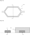
- the measuring arm B2 has an upper surface in contact with an ambient medium MA, for example a saline solution likely to contain biomolecules, while the reference arm B1 is separated from the ambient medium by a surface coating RS with a thickness much greater than L d , typically at least by a factor of 5, or even by a factor of 10.
- the upper surface of the waveguide forming the measuring arm B2 comprises a functionalization layer CF adapted to selectively fix or adsorb a target biological species (bacteria, virus, etc.) or chemical species (protein, nucleic acid, etc.). If the target biological or chemical species is present in the ambient medium, the refractive index "seen" by a light wave propagating in the measuring arm changes. This induces a phase shift relative to the light wave propagating in the reference arm, and therefore a variation in the light intensity at the output of the interferometer.
- an ambient medium MA for example a saline solution likely to contain biomolecules
- the reference arm B1 is separated from the ambient medium by
- the B1 and B2 arms of the interferometer are usually spirally wound to increase their length while maintaining the compactness of the device.
- a disadvantage of the architecture illustrated on the [ Fig. 1A] and [Fig. 1B ] is that it does not allow to differentiate a change in the refractive index of the ambient medium in volume (“bulk”) - for example caused by a change in water salinity or a change in air pressure - from an adsorption of molecules on the surface.
- the sensor signal is therefore ambiguous and tainted with error or uncertainty if the two phenomena appear simultaneously, which is often the case in practice.
- a known solution to this problem is to normalize the signal of the "interest” sensor by a so-called reference sensor, whose measuring arm is not functionalized, or is even treated to minimize adsorption (so-called “blocking” or “anti-fouling” coating, for example based on casein).
- This approach is used, for example, in the field of surface plasmon resonance sensors, see (Karlsson 1995).
- This solution requires very good chemical or biochemical recognition specificity for the sensor of interest and very good blocking for the reference sensor. In practice, it works well when the concentrations of target molecules (or those of any interferents) involved are quite low and the temporal variations of the optical index of the ambient medium (for example, when replacing a first solution to be analyzed with a rinsing buffer solution, then with a second solution to be analyzed) remain limited. When these two conditions are not met, normalization is no longer effective and a spurious signal persists.
- US 2007/0076212 discloses a device for examining atheromatous plaques by optical coherence tomography, based on a Michelson interferometer, one arm of which consists of two optical fibers intended to be introduced into a blood vessel by means of a catheter. The light emerges from the end of a first optical fiber and a mirror directs it towards the atheroma. The light backscattered by the latter is reflected by another mirror to be coupled into a second optical fiber. This sensor does not allow the measurement of a variation in the optical index of a medium.
- JP 2018066664 discloses an interferometric sensor comprising an integrated Mach-Zender interferometer, the two arms of which are formed by planar waveguides which cross a fluidic channel. This sensor is intended solely for carrying out absorption spectroscopy measurements.
- the invention aims to overcome at least in part the aforementioned drawbacks of the prior art. More particularly, it aims to provide a photonic sensor making it possible to decorrelate in a simple and effective manner the effects of changes in volume and surface refractive index.
- this aim is achieved by using an interferometer which can be described as “hybrid” because the reference arm is a waveguide, while the measuring arm has a portion propagating in free space in the ambient medium.
- An object of the invention is therefore a photonic sensor according to claim 1.
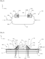
- a photonic sensor CP1 according to a first embodiment of the invention is described below with reference to the [ Fig. 2 ] - plan view - and to the [ Fig. 4], [Fig. 5 ] And [ Fig. 6 ] - sectional views of different variants.
- the photonic sensor CP1 comprises an interferometer I1 having a first arm BR1 and a second arm BR2.
- the first arm BR1 comprises a first optical waveguide G1 and a second optical waveguide G1', separated from the first optical guide G1 by a gap.
- the second arm BR2 comprises an optical waveguide G2.
- the first arm BR1 comprises at least a first coupling device DC1 between a guided propagation mode in the first optical waveguide G1 and a free propagation mode in an ambient medium MA.
- the first arm BR1 also comprises a second coupling device DC2, distinct from said first coupling device DC1, between said free propagation mode in the ambient medium MA and the guided propagation mode in the second optical waveguide G1'.
- Said first coupling device DC1 is configured to extract a light wave from the first waveguide G1' and said second coupling device DC2 to reinject it into the second waveguide G1'.
- the first BR1 arm further includes an SO1 optical system.
- the optical system SO1 is configured to direct said free propagation mode towards said second coupling device DC2.
- the first and second coupling devices DC1, DC2 and the optical system SO1 of the first arm BR1 allow a light wave passing through said first arm BR1 to carry out a part trMA of its path in said ambient medium MA, corresponding to the interval separating the first waveguide G1 from the second waveguide G1'.
- the optical waveguides G1 and/or G1' can be planar waveguides.
- the first coupling device DC1 may be a diffraction grating, in particular integrated in a planar layer CO1 comprising the first optical waveguide G1.
- the second coupling device DC2 may be a diffraction grating, in particular integrated in a planar layer CO1 comprising the second optical waveguide G1'.
- the first arm BR1 can be a measuring arm and the second arm BR2 can be a reference arm.
- the interferometer I is for example of the Mach-Zehnder type.
- a photonic sensor CP11 according to a first variant of the first embodiment is described below in relation to the [ Fig. 3 ].
- the optical waveguide G1 of the first arm BR1 of the photonic sensor CP1 is for example arranged on a substrate S1.
- the optical waveguide G1 may be located in a planar layer CO1 covering a face of the substrate S1.
- the surface of the interferometer intended to be placed in contact with the ambient medium MA may comprise at least a portion of the face FL of the planar layer CO1 opposite the face FS of the planar layer CO1 in contact with the substrate S1.
- the planar layer CO1 may comprise a stack of a first layer CO11 and a second layer CO21.
- the first layer CO11 is for example made of silicon.
- the second layer CO21 may comprise at least one dielectric material, for example silicon oxide.
- the optical waveguide G1 may be located in the second layer CO21.
- the optical system SO1 comprises a first optical reflector R1 and a second optical reflector R2.
- the first optical reflector R1 is configured to direct the light wave extracted from the first waveguide G1 by the first coupling device DC1 towards the second optical reflector R2.
- the second optical reflector R2 is configured to direct at least a portion of the light wave towards the second coupling device DC2 reinjecting it into the second waveguide G1'.
- the first optical reflector R1 comprises a prism PR1.
- the second optical reflector R2 comprises a prism PR2.
- the first optical reflector R1 comprises a first face F11, a second face F12, a third face F13.
- the second optical reflector R2 comprises a first face F21, a second face F22, a third face F23.
- the first face F11 of the first optical reflector R1 is located opposite the first coupling device DC1.
- the second face F12 of the first optical reflector R1 is inclined relative to the first face F11, in particular by an angle equal to 45° or substantially equal to 45°.
- the first face F11 of the first optical reflector R1 may be in contact with the face FL of the planar layer CO1.
- the first face F21 of the second optical reflector R2 is located opposite the second coupling device DC2.
- the second face F12 of the first optical reflector R1 is configured to reflect the light wave extracted from the first waveguide G1, in particular towards the second face F22 of the second optical reflector R2.
- the second face F22 of the second optical reflector R2 is configured to reflect the light wave, in particular towards the second coupling device DC2.
- the first face F21 of the second optical reflector R2 may be in contact with the face FL of the planar layer CO.
- the third face F13 of the first optical reflector R1 is arranged opposite the third face F23 of the second optical reflector R2.
- the first and second coupling devices DC1, DC2 may be arranged in the photonic circuit such that the third face F13 of the first optical reflector R1 is located at a distance from the third face F23 of the second optical reflector R2.
- the distance F13 - F12 is typically at least 1 mm and may reach 1 cm, or even several centimeters.
- a light wave passing through the first arm BR1 makes part of its journey in the ambient medium MA, in particular between the third face F13 of the first optical reflector R1 and the third face F23 of the second optical reflector R2.
- the third face F13 of the first optical reflector R1 may be perpendicular or substantially perpendicular (within the limits of manufacturing tolerances) to the face FL of the planar layer CO.
- the third face F23 of the second optical reflector R2 may be perpendicular or substantially perpendicular (within the limits of manufacturing tolerances) to the face FL of the planar layer CO.
- the first coupling device DC1 may comprise a diffraction grating RD11 configured to diffract the light wave propagating in the first waveguide G1 in a direction perpendicular to the free face FL of the latter.
- a grating is known in particular from (Zhang 2019).
- the second coupling device DC2 may comprise a diffraction grating RD12 configured to diffract the light wave propagating in free space in a direction perpendicular to the free face FL of the second waveguide G1' to couple it to a guided mode of the latter.
- the second face F22 of the second optical reflector R2 is inclined relative to the first face F21, in particular by an angle equal to 45° or substantially equal to 45°.
- the RD11 and RD12 diffraction gratings can be fabricated by known laser etching or direct writing techniques.
- a CP12 photonic sensor according to a second variant of the first embodiment is described below in relation to the [ Fig. 4 ]. Elements common to those of the CP11 photonic sensor are designated by the same references and are not described again below.
- the first coupling device DC1 comprises a diffraction grating RD21.
- the second coupling device DC2 comprises a diffraction grating RD22.
- the diffraction gratings RD21 and RD22 are configured to diffract the light wave propagating in the waveguide in a direction forming an angle of approximately 8° relative to the free face FL of the latter.
- the first optical reflector R1 comprises a prism PR12.
- the second optical reflector R2 comprises a prism PR22.
- the PR12 prism comprises a first face F112, a second face F122, a third face F132.
- the PR22 prism comprises a first face F212, a second face F222, a third face F232.
- the first face F112 of the prism PR12 is located opposite the first coupling device DC1.
- the second face F122 of the prism PR12 is inclined relative to the first face F112.
- the first face F212 of the prism PR22 is located opposite the second coupling device DC2.
- the second face F222 of the prism PR22 is inclined relative to the first face F212.
- the second face F122 of the prism PR12 is configured to reflect the light wave extracted from the first waveguide G1, in particular towards the second face F222 of the prism PR22.
- the second face F222 of the prism PR22 is configured to reflect the light wave, in particular towards the second coupling device DC2.
- the third face F132 of the prism PR12 is arranged opposite the third face F232 of the prism PR22.
- the reflecting faces F122 and F222 are inclined at an angle equal to 41° or substantially equal to 41° relative to the first faces F112, F212, respectively.
- a photonic sensor CP13 according to a third variant of the first embodiment is described below in relation to the [ Fig. 5 ]. Elements common to those of the CP1 photonic sensor and/or the CP2 photonic sensor are designated by the same references and are not described again below.
- the first optical reflector R1 comprises a prism PR13 having a first face F113, a second face F123, a third face F133.
- the second optical reflector R2 comprises a prism PR23 having a first face F213, a second face F223, a third face F233.
- the first face F113 of the prism PR13 is located opposite the first coupling device DC1.
- the second face F123 of the prism PR13 is inclined relative to the first face F113.
- the first face F213 of the prism PR13 is located opposite the second coupling device DC2.
- the second face F223 of the prism PR23 is inclined relative to the first face F213.
- the inclination of the faces F123 and F223 is chosen according to the diffraction angles of the diffraction gratings so that the light wave reflected on the second face F123 of the prism PR13 propagates in a parallel or substantially parallel manner to the plane (X, Y).
- the second face F123 of the prism PR13 is configured to reflect the light wave extracted from the first waveguide G1, in particular towards the second face F223 of the lens L2.
- the second face F223 of the prism PR23 is configured to reflect the light wave, in particular towards the second coupling device DC2.
- the third face F133 of the prism PR13 1 is arranged opposite the third face F233 of the prism PR23.
- the third face F133 of the prism PR13 is convex, so as to form a converging lens L1 adapted to collimate the light beam coming from the coupling device DC1 and reflected by the second face F123.
- the third face F233 of the prism PR23 is convex, so as to form a converging lens L2.
- the lens L2 is intended to focus the light wave towards the second coupling device DC2.
- a CP14 photonic sensor according to a fourth variant of the first embodiment is described below in relation to the [ Fig. 6 ]. Elements common to those of the photonic sensor CP1 and/or the photonic sensor CP2 and/or the photonic sensor CP3 are designated by the same references and are not described again below.
- the first optical reflector R1 comprises a PR14 prism.
- the second optical reflector R2 comprises a PR24 prism.
- the PR14 prism comprises a first face F114, a second face F124, a third face F134.
- the PR24 prism comprises a first face F214, a second face F224, a third face F234.
- the first face F114 of the prism PR14 is located opposite the first coupling device DC1.
- the second face F124 of the prism PR14 is inclined relative to the first face F114.
- the first face F214 of the prism PR24 is located opposite the second coupling device DC2.
- the second face F224 of the prism PR24 is inclined relative to the first face F214.
- the second face F124 of the prism PR14 is configured to reflect the light wave extracted from the first waveguide G1, in particular towards the second face F224 of the prism PR24.
- the second face F224 of the prism PR24 is configured to reflect the light wave, in particular towards the second coupling device DC2.
- the third face F134 of the prism PR14 is arranged opposite the third face F234 of the prism PR24.
- the second face F124 of the prism PR14 can be concave, on the side oriented towards the first coupling device DC1, in particular to focus or collimate the light wave by reflecting it.
- the second face F224 of the prism PR24 can be concave, on the side facing the second coupling device DC2, in particular to collimate the light wave by reflecting it.
- the inclination of the faces F124 and F224 is chosen according to the diffraction angles of the diffraction gratings so that the light wave reflected on the second face F123 of the reflector R1 propagates in a manner parallel or substantially parallel to the plane (X, Y).
- the third variant of the first embodiment can be combined with the first, second or fourth variant of the first embodiment.
- the light wave extracted from the first waveguide G1 can be reflected on the second face F12, F122, F123, F124 of the first optical reflector R1 by total internal reflection.
- the light wave can then also be reflected on the second face F22, F222, F223, F224 of the second optical reflector R2 by total internal reflection.
- the second face F12, F122, F123, F124 of the first optical reflector R1 may be covered with a reflective layer or a reflective coating or a reflective thin film CR1, on the side of the second face F12, F122, F123, F124 facing the first coupling device DC1.
- the reflective layer CR1 may comprise at least one metallic material, for example gold.
- the second face F22, F222, F223, F224 of the second optical reflector R2 may be covered with a reflective layer or a reflective coating or a reflective thin film CR2, on the side of the second face F22, F222, F223, F224 facing the second coupling device DC2.
- the reflective layer CR2 may comprise at least one metallic material, for example gold.
- the first optical reflector R1 and the second optical reflector R2 can be manufactured by three-dimensional printing, also called 3D printing, in particular exploiting two-photon polymerization as described by (Dietrich 2018) or direct laser writing as described by (Malinauskas 2012).
- a photonic sensor C2 according to a second embodiment of the invention is described below with reference to the [ Fig. 7 ].
- This second embodiment differs from the first embodiment essentially by the structure of the optical system allowing the free propagation of the light wave in the ambient environment.
- the photonic sensor C2 comprises an interferometer I2, for example of the Mach-Zehnder type, having a first arm BR12 and a second arm.
- the first arm BR12 comprises an optical waveguide G12.
- the first arm BR12 comprises a first coupling device DC12 between a guided propagation mode in the waveguide and a free propagation mode in an ambient medium MA.
- the first arm BR12 comprises a second coupling device DC22 between said free propagation mode in the ambient medium and a guided propagation mode in the waveguide G12.
- the second coupling device DC22 is in particular distinct from said first coupling device DC12.
- the first and second coupling devices DC12, DC22 may be diffraction gratings.
- the first arm BR12 comprises an optical system SO2 configured to direct said free propagation mode towards said second coupling device DC2.
- the first BR12 arm can be a measuring arm and the second arm can be a reference arm.
- the second arm may have a surface that can be brought into contact with an ambient medium MA and having a functionalization layer allowing the specific fixation of chemical or biological species.
- the G12 optical waveguide can be a planar waveguide.
- the first coupling device DC12 is in particular configured to extract a light wave from the waveguide G12.
- the second coupling device DC22 is in particular configured to reinject the light wave into the waveguide G12.
- the optical system SO2 of the first arm BR12 comprises a first optical reflector R12 and a second optical reflector R22.
- the G12 optical waveguide is for example arranged on an S12 substrate.
- the optical waveguide G12 may be located in a planar layer CO2 covering a face of the substrate S12.
- the surface of the interferometer I intended to be placed in contact with an ambient medium MA may comprise at least a portion of the face FL2 of the planar layer CO2 opposite the face FS2 of the planar layer CO in contact with the substrate S12.
- the planar CO2 layer may comprise a stack of a first CO12 layer and a second CO22 layer.
- the first CO12 layer is for example made of silicon.
- the second CO22 layer may comprise at least one dielectric material, for example silicon oxide.
- the optical waveguide G12 may be located in the second CO22 layer.
- the first optical reflector R12 is configured to direct the light wave extracted from the optical waveguide G12 by the first coupling device DC12 towards the second optical reflector R22, which is itself configured to direct said light wave towards the second coupling device DC22 reinjecting it into the waveguide G12.
- the first optical reflector R12 comprises an inclined face FI1.
- the second optical reflector R22 comprises an inclined face FI2.
- the inclined face FI1 of the first optical reflector R12 is configured to reflect the light wave extracted from the waveguide G12, in particular towards the inclined face FI2 of the second optical reflector R22.
- the inclined face FI2 of the second optical reflector R22 is configured to reflect the light wave, in particular towards the second coupling device DC22.
- the inclined face FI1 and the inclined face FI2 of the first and second optical reflectors R12, R22, respectively, are in particular formed from first and second side walls PL1, PL2 of a trench T obtained by anisotropic wet etching of a monocrystalline substrate or a monocrystalline layer S2, for example made of silicon.
- the inclined face FI1 of the first optical reflector R12 may be inclined relative to the face FL2 of the planar layer CO2, in particular by an angle equal to 54.7° or substantially equal to 54.7°, which corresponds to the orientation of a crystalline plane ⁇ 1 1 1 ⁇ of a silicon substrate.
- the first and second optical reflectors R12, R22 form or delimit, with the waveguide G12, a fluid conduit CF for said ambient medium MA.
- a light wave OL passing through said first arm BR12 carries out part of its path in said ambient medium MA, inside the fluid conduit CF.
- the CF fluid conduit is, for example, a micro-fluid conduit.
- a micro-conduit is understood to mean a conduit with millimeter or sub-millimeter dimensions.
- the inclined face FI1 of the first optical reflector R12 and the inclined face FI2 of the second optical reflector R22 may be covered with a reflective layer or a reflective coating or a reflective thin film, on the side facing the first coupling device DC12 and on the side facing the second coupling device DC12. DC12 coupling, respectively.
- the reflective layer may comprise at least one metallic material, for example gold.
- the reflective layer may be of the Bragg mirror type, formed in particular by a plurality of flat silicon oxide (SiO2) surfaces and by a plurality of flat silicon nitride (SiN) surfaces.
- the T trench can be made by wet etching.
- an SU surface extending along a ⁇ 100 ⁇ or ⁇ 010 ⁇ or ⁇ 001 ⁇ crystal plane of a monocrystalline silicon substrate is covered with an HM mask. Chemical etching is then carried out through an opening in the mask.
- the trench T comprises a first sidewall PL1 and a second sidewall PL2.
- the anisotropic wet etching can be carried out so that the first and second sidewalls PL1, PL2 extend along a ⁇ 111 ⁇ crystal plane.
- the trench T may further comprise a bottom F which may further delimit the fluid conduit CF after assembly of at least a portion of the monocrystalline layer or of the monocrystalline substrate S2 on the layer CO2.
- the fluid conduit CF may have a trapezoidal section in a plane (X, Z).
- the bottom F may be covered with a reflective layer or a reflective coating or a reflective thin film, in particular the same layer as that covering the first and second inclined faces FI1, FI2.
- An advantage of a C2 photonic sensor of the type described in connection with the [ Fig. 7 ] is related to the fact that it is quick to manufacture and has a low cost.
- An advantage of such a photonic sensor C2 lies in the fact that a plurality, in particular thousands, of first and second optical reflectors R12, R22 and fluidic conduits CF can be produced simultaneously on the same substrate S12.
- a plurality, in particular thousands, of first and second optical reflectors R12, R22 can be assembled simultaneously with a CO2 layer comprising a waveguide G12 and covering the same substrate S12, for example by means of a single step of bonding the substrate or the layer S2 onto the substrate S12 with interposition of the optical waveguide G12.
- An advantage of such a photonic sensor C2 is linked to the fact that the inclination of the first and second optical reflectors R12, R22 relative to the optical waveguide G12 can be identical or substantially identical for a plurality of first and second optical reflectors R12, R22 arranged on the same substrate S12 or on different substrates S12, thanks to the fact that this inclination depends on the crystalline structure of the substrate S2.
- the diffraction gratings of coupling devices DC12 and DC22 must be adapted to these inclinations, but this does not pose any particular difficulty.
- the assembly of the first and second optical reflectors R12, R22 on the substrate S12 with interposition of the optical waveguide G12 can be carried out by bonding, preferably at room temperature - for example bonding by polymer adhesive (UV glue), deposited for example by screen printing - in order to ensure compatibility with functionalization by biomolecules.
- bonding preferably at room temperature - for example bonding by polymer adhesive (UV glue), deposited for example by screen printing - in order to ensure compatibility with functionalization by biomolecules.
- UV glue polymer adhesive
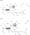
- a photonic sensor C31 according to a first variant of a third embodiment is described below with reference to the [ Fig. 8 ].
- the photonic sensor C31 comprises an interferometer I3 having a first arm BR13 and a second arm BR23.
- the first arm BR13 comprises an optical waveguide G13.
- the second arm BR23 comprises an optical waveguide G23.
- the first arm BR13 comprises a coupling device DC3 between a guided propagation mode in the optical waveguide G13 and a free propagation mode in an ambient medium MA.
- the first arm BR13 comprises an optical system SO3 configured to direct said free propagation mode towards said coupling device DC3 between said free propagation mode in the ambient medium and a guided propagation mode in the optical waveguide G13.
- a light wave OL passing through said first arm BR13 makes part of its journey in said ambient medium MA.
- the first arm BR13 can be a measuring arm and the second arm BR23 can be a reference arm.
- the DC3 coupling device can be a diffraction grating.
- the second arm BR23 may have a surface that can be brought into contact with said ambient medium MA and having a functionalization layer allowing the specific fixation of chemical or biological species.
- the G13 optical waveguide can be a planar waveguide.
- the G23 optical waveguide can be a planar waveguide.
- the interferometer I3 may be a Michelson-type interferometer.
- the first arm BR13 comprises a single coupling device DC3 configured to extract a light wave from the optical waveguide G13 and to reinject it into the optical waveguide G13 after reflection by an optical reflector R3 of an optical system SO3, spaced from said coupling device DC3.
- a light wave OL passing through said first arm BR13 thus completes part of its path in said ambient medium MA.
- the DC3 coupling device is intended to achieve coupling between a guided propagation mode in the G13 optical waveguide and a free propagation mode in an ambient medium MA.
- the optical system SO3 is configured to direct said free propagation mode towards said coupling device DC3.
- the second arm BR23 of the I3 interferometer can include a mirror M.
- the mirror M is formed by a loop of the optical waveguide G23, notably located in a planar layer CO3.
- the interferometer I3 may comprise a splitter SE3, implemented for example by means of a multimode interferometer, for separating a light wave OL coming from an input port into a first component directed towards the first arm BR13 and a second component directed towards the second arm BR23, and for recombining the light waves coming from the first and second arms and directing them towards an output port.
- a splitter SE3 implemented for example by means of a multimode interferometer, for separating a light wave OL coming from an input port into a first component directed towards the first arm BR13 and a second component directed towards the second arm BR23, and for recombining the light waves coming from the first and second arms and directing them towards an output port.
- a photonic sensor C32 according to a second variant of the third embodiment is described below with reference to the [ Fig. 9 ]. Common elements with those of the first variant of the third embodiment are designated by the same references.
- the mirror M comprises a Bragg mirror MB, notably formed by an alternation of materials with different refractive indices, separated by flat surfaces.
- a photonic sensor C33 according to a third variant of the third embodiment is described below with reference to the [ Fig. 10 ]. Elements common to those of the first and second variants of the third embodiment are designated by the same references.
- the interferometer I3 comprises a circulator CI3 instead of the separator SE3 produced by means of a multimode interferometer.
- the circulator CI3 has lower losses than a multimode interferometer, but its production - particularly integrated - is more complex.
- the mirror M can be formed by a loop of the optical waveguide G23, in particular located in a planar layer CO3.
- a first variant of the first arm BR13 of an interferometer I3 of a photonic sensor C311 according to the third embodiment of the invention is described below with reference to the [ Fig. 11 ].
- the optical waveguide G13 of the first arm BR13 of the photonic sensor C311 is for example arranged on a substrate S3.
- the G13 optical waveguide can be formed in a CO3 planar layer.
- the planar layer CO3 may comprise a stack of a first layer CO13 and a second layer CO23.
- the first layer CO13 is for example made of silicon.
- the second layer CO22 may comprise at least one dielectric material, for example silicon oxide.
- the optical waveguide G13 may be located in the second layer CO23.
- the optical reflector R3 may comprise a mirror, for example planar.
- the optical reflector R3 comprises a reflective face F311 opposite the optical waveguide G13.
- the optical reflector R3 and the optical waveguide G13 are for example separated by a distance d.
- the distance d is for example of the order of 150 micrometers.
- the optical reflector R3 can be formed in a planar layer delimiting with the optical waveguide G13 a microchannel for the ambient medium MA.
- the DC3 coupling device may comprise an RD311 diffraction grating.
- the diffraction grating RD311 is in particular configured to diffract the light wave propagating in the waveguide in a direction perpendicular to the free face of the latter perpendicular to the X, Y plane.
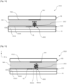
- a second variant of the first arm BR13 of an interferometer I3 of a photonic sensor C312 according to the third embodiment of the invention is described below with reference to the [ Fig. 12 ]. Elements in common with those of the variant described with reference to the [ Fig. 11 ] are designated by the same references.
- the optical system SO3 may include a converging lens L312.
- the converging lens L312 is intended to focus or collimate the light wave OL.
- the L312 converging lens for example, is an aspherical lens.
- a third variant of the first arm BR13 of an interferometer I3 of a photonic sensor C313 according to the third embodiment of the invention is described below with reference to the [ Fig. 13 ]. Elements in common with those of the variants described with reference to [ Fig. 11 ] And [ Fig. 12 ] are designated by the same references.
- the optical system SO3 may include a converging lens L313.
- the converging lens L313 is intended to focus or collimate the light wave OL.
- the L313 converging lens is, for example, a converging lens of any shape.
- the shape of the L313 converging lens can be chosen depending on the DC3 coupling device.
- the DC3 coupling device may comprise an RD313 diffraction grating.
- the RD313 diffraction grating and the L313 converging lens can be configured so that the light extracted from the G13 optical waveguide propagates perpendicularly or substantially perpendicularly to the (X, Y) plane, even if the RD313 diffraction grating is configured to diffract a light wave propagating in the one guide in a direction which is not perpendicular to the (X, Y) plane.
- the reflective face F311 of the optical reflector R3 may be at least partially covered with a reflective layer or a reflective coating or a reflective thin film CR3.
- the reflective layer CR3 may comprise at least one metallic material, for example gold.
- the reflective layer CR3 may be located opposite the coupling device DC3.
- the second arm of the interferometer is isolated from the ambient medium, for example by an oxide layer.
- the interferometric signal therefore makes it possible to determine the optical volume index of the ambient medium.
- a prior art Mach-Zehnder interferometer serving as a biosensor and having a 1 cm long sensitive arm has a bulk limit of detection (LoD) of the order of 1 ⁇ 10 -6 RIU.
Landscapes
- Physics & Mathematics (AREA)
- Nonlinear Science (AREA)
- General Physics & Mathematics (AREA)
- Chemical & Material Sciences (AREA)
- Optics & Photonics (AREA)
- Immunology (AREA)
- General Health & Medical Sciences (AREA)
- Biochemistry (AREA)
- Analytical Chemistry (AREA)
- Pathology (AREA)
- Life Sciences & Earth Sciences (AREA)
- Health & Medical Sciences (AREA)
- Engineering & Computer Science (AREA)
- Chemical Kinetics & Catalysis (AREA)
- Plasma & Fusion (AREA)
- Optical Integrated Circuits (AREA)
- Investigating Or Analysing Materials By Optical Means (AREA)
Abstract
- au moins un premier dispositif de couplage (DC1) entre un mode de propagation guidé dans le guide d'onde (G1) et un mode de propagation libre dans un milieu ambiant (MA) ; et
- un système optique (SO1) configuré pour diriger ledit mode de propagation libre vers ledit ou un deuxième dispositif de couplage (DC2) entre ledit mode de propagation libre dans le milieu ambiant (MA) et un mode de propagation guidé dans le guide d'onde (G1) ;
moyennant quoi une onde lumineuse traversant ledit premier bras effectue une partie (trMA) de son trajet dans ledit milieu ambiant ;
caractérisé en ce que ledit ou chaque dit dispositif de couplage comprend un réseau de diffraction.
Description
- L'invention se situe dans le domaine des capteurs photoniques, et plus particulièrement dans le domaine des capteurs dont la mesurande est déduite d'une mesure de variation d'indice optique d'un milieu ambiant. La mesurande peut être par exemple une concentration de molécules cibles dans un gaz ou liquide (capteur de gaz, biocapteur...), ou directement l'indice optique d'un milieu (réfractomètre). Avantageusement, l'invention est mise en oeuvre au moyen de circuits photoniques intégrés, c'est-à-dire basée sur des guides d'onde diélectriques planaires.
- Par guide d'onde planaire, on entend un guide d'onde formé dans une couche planaire d'un dispositif optoélectronique. Un guide d'onde planaire peut avoir notamment une section rectangulaire.
- Il est connu que l'onde électromagnétique qui se propage dans un guide d'onde diélectrique présente un champ évanescent qui s'étend sur une distance appelée la longueur de pénétration Ld (ou d1/e) autour du guide. Ld correspond à la distance à laquelle l'intensité du champ électrique est divisée par la constante e. Ld dépend de la longueur d'onde et des indices optiques des milieux vus par la lumière, et vaut typiquement 75 à 150 nm pour λ = (750 nm -1500 nm) avec des guides en SiN ou Si dans l'air. D'une manière générale, on a

- Seuls les changements d'indice optique ayant lieu dans cette zone seront susceptibles de provoquer un changement d'indice effectif du mode guidé. Ainsi, même des couches sub-nanométriques de molécules adsorbées ou capturées en surface d'un guide peuvent provoquer un changement d'indice effectif mesurable. Cela est possible car l'indice de réfraction des molécules est différent (en général supérieur) à l'indice de réfraction du milieu couvrant, typiquement : nair = 1, neau = 1,33, nbiomolecule = 1,45.
- Cet effet est exploité, par exemple, pour réaliser des biocapteurs photoniques intégrés, comme illustré sur les [
Fig. 1A ] (vue en plan) et [Fig. 1B ] (vue en coupe AA). Ces figures représentent, de manière très schématique, un interféromètre de Mach-Zehnder intégré (MZI) comprenant un bras « de référence » B1 et un bras « de mesure » B2. - Le bras de mesure B2 présente une surface supérieure en contact avec un milieu ambiant MA, par exemple une solution saline susceptible de contenir des biomolécules, tandis que le bras de référence B1 est séparé du milieu ambiant par un revêtement de surface RS d'épaisseur très supérieure à Ld, typiquement au moins d'un facteur 5, voire d'un facteur 10. Avantageusement, la surface supérieure du guide d'onde formant le bras de mesure B2 comporte une couche de fonctionnalisation CF adaptée pour fixer ou adsorber sélectivement une espèce biologique (bactérie, virus...) ou chimique (protéine, acide nucléique...) cible. Si l'espèce biologique ou chimique cible est présente dans le milieu ambiant, l'indice de réfraction « vu » par une onde lumineuse se propageant dans le bras de mesure change. Cela induit un déphasage par rapport à l'onde lumineuse se propageant dans le bras de référence, et donc une variation de l'intensité lumineuse à la sortie de l'interféromètre.
- En réalité, les bras B1 et B2 de l'interféromètre sont généralement enroulés en spirale pour augmenter leur longueur tout en maintenant la compacité du dispositif.
- (Laplatine 2022) décrit un capteur olfactif basé sur un réseau de 64 capteurs photoniques individuels du type des figures [
Fig. 1A] et [Fig. 1B ]. - Un inconvénient de l'architecture illustrée sur les [
Fig. 1A] et [Fig. 1B ] est qu'elle ne permet pas de différencier un changement d'indice de réfraction du milieu ambiant en volume (« bulk ») - par exemple causé par un changement de salinité de l'eau ou un changement de pression de l'air - d'une adsorption de molécules en surface. Le signal du capteur est donc ambigu et entaché d'erreur ou d'incertitude si les deux phénomènes apparaissent simultanément, ce qui est en pratique souvent le cas. - Une solution connue à ce problème consiste à normaliser le signal du capteur « d'intérêt » par un capteur dit de référence, dont le bras de mesure n'est pas fonctionnalisé, voire est traité pour minimiser l'adsorption (revêtement dit « de blocage » ou « anti-fouling », par exemple à base de caséine). Cette approche est utilisée, par exemple, dans le domaine des capteurs à résonance plasmonique de surface, voir (Karlsson 1995).
- Cette solution nécessite une très bonne spécificité de reconnaissance chimique ou biochimique pour le capteur d'intérêt et un très bon blocage pour le capteur de référence. En pratique, elle fonctionne bien quand les concentrations de molécules cibles (ou celles des éventuels interférents) mises en jeu sont assez faibles et que les variations temporelles de l'indice optique du milieu ambiant (par exemple, lorsqu'on remplace une première solution à analyser par une solution tampon de rinçage, puis par une deuxième solution à analyser) restent limitées. Lorsque ces deux conditions ne sont pas réunies, la normalisation n'est plus efficace et un signal parasite persiste.
- (Ignatyeva 2021) propose de différencier les effets des indices de réfraction de volume et de surface en utilisant un cristal magnétophotonique. Il s'agit là d'une solution très complexe à mettre en oeuvre, qui nécessite l'utilisation de matériaux « exotiques » et un champ magnétique externe.
-
US 2007/0076212 divulgue un appareil pour examiner les plaques d'athérome par tomographie de cohérence optique, basé sur un interféromètre de Michelson dont un bras est constitué par deux fibres optiques destinées à être introduites dans un vaisseau sanguin au moyen d'un cathéter. La lumière sort du bout d'une première fibre optique et un miroir la dirige vers l'athérome. La lumière rétrodiffusée par ce dernier est réfléchie par un autre miroir pour être couplée dans une seconde fibre optique. Ce capteur ne permet pas de mesurer une variation d'indice optique d'un milieu. -
JP 2018066664 - L'invention vise à surmonter au moins en partie les inconvénients précités de l'art antérieur. Plus particulièrement elle vise à procurer un capteur photonique permettant de décorréler de manière simple et efficace les effets des changements d'indice de réfraction de volume et de surface.
- Conformément à l'invention, ce but est atteint grâce à l'utilisation d'un interféromètre que l'on peut qualifier d'« hybride » car le bras de référence est un guide d'onde, tandis que le bras de mesure comporte une portion en propagation en espace libre dans le milieu ambiant.
- Un objet de l'invention est donc un capteur photonique selon la revendication 1.
- Des modes de réalisation particuliers de l'invention font l'objet des revendications dépendantes.D'autres caractéristiques, détails et avantages de l'invention ressortiront à la lecture de la description faite en référence aux dessins annexés donnés à titre d'exemple et qui représentent, respectivement :
- [
Fig.1A] et [Fig. 1B ], déjà décrites, une vue en plan et en coupe AA, respectivement, d'un capteur photonique selon l'art antérieur ; - [
Fig. 2 ], une vue en plan d'un capteur selon un premier mode de réalisation de l'invention ; - [
Fig. 3 ], [Fig. 4 ], [Fig. 5 ] et [Fig. 6 ] des vues en coupe de capteurs selon quatre variantes dudit premier mode de réalisation de l'invention ; - [
Fig. 7 ], une vue en coupe d'un capteur selon un deuxième mode de réalisation de l'invention ; - [
Fig. 8], [Fig. 9 ], [Fig. 10 ] des vues en plan de capteurs de diverses variantes d'un troisième mode de réalisation de l'invention ; et - [
Fig. 11 ], [Fig. 12] et [Fig. 13 ], des vues de détail en coupe de diverses variantes dudit troisième mode de réalisation de l'invention. - Un capteur photonique CP1 selon un premier mode de réalisation de l'invention est décrit ci-après en référence à la [
Fig. 2 ] - vue en plan - et aux [Fig. 4], [Fig. 5 ] et [Fig. 6 ] - vues en coupe de différentes variantes. - On définit un repère orthogonal X, Y, Z dans lequel le plan (X, Y) est le plan selon lequel une surface principale d'un substrat s'étend.
- Le capteur photonique CP1 comprend un interféromètre I1 ayant un premier bras BR1 et un deuxième bras BR2. Le premier bras BR1 comprend un premier guide d'onde optique G1 et un second guide d'onde optique G1', séparé du premier guide optique G1 par un intervalle. Le deuxième bras BR2 comprend un guide d'onde optique G2.
- Le premier bras BR1 comprend au moins un premier dispositif de couplage DC1 entre un mode de propagation guidé dans le premier guide d'onde optique G1 et un mode de propagation libre dans un milieu ambiant MA.
- Le premier bras BR1 comprend également un deuxième dispositif de couplage DC2, distinct dudit premier dispositif de couplage DC1, entre ledit mode de propagation libre dans le milieu ambiant MA et le mode de propagation guidé dans le second guide d'onde optique G1'.
- Ledit premier dispositif de couplage DC1 est configuré pour extraire une onde lumineuse du premier guide d'onde G1' et ledit deuxième dispositif de couplage DC2 pour la réinjecter dans le second guide d'onde G1'.
- Le premier bras BR1 comprend en outre un système optique SO1.
- Le système optique SO1 est configuré pour diriger ledit mode de propagation libre vers ledit deuxième dispositif de couplage DC2.
- Les premier et deuxième dispositifs de couplage DC1, DC2 et le système optique SO1 du premier bras BR1 permettent à une onde lumineuse traversant ledit premier bras BR1 d'effectuer une partie trMA de son trajet dans ledit milieu ambiant MA, en correspondant de l'intervalle séparant le premier guide d'onde G1 du second guide d'onde G1'.
- Les guides d'onde optiques G1 et/ou G1' peuvent être des guides d'ondes planaires.
- Le premier dispositif de couplage DC1 peut être un réseau de diffraction, notamment intégré dans une couche planaire CO1 comprenant le premier guide d'onde optique G1. Le deuxième dispositif de couplage DC2 peut être un réseau de diffraction, notamment intégré dans une couche planaire CO1 comprenant le second guide d'onde optique G1'.
- Le premier bras BR1 peut être un bras de mesure et le deuxième bras BR2 peut être un bras de référence.
- Selon le premier mode de réalisation, l'interféromètre I est par exemple de type Mach-Zehnder.
- Un capteur photonique CP11 selon une première variante du premier mode de réalisation est décrit ci-après en relation avec la [
Fig. 3 ]. - Le guide d'onde optique G1 du premier bras BR1 du capteur photonique CP1 est par exemple agencé sur un substrat S1.
- Le guide d'onde optique G1 peut être situé dans une couche planaire CO1 recouvrant une face du substrat S1. La surface de l'interféromètre destinée à être mise en contact avec le milieu ambiant MA peut comprendre au moins une portion de la face FL de la couche planaire CO1 opposée à la face FS de la couche planaire CO1 en contact avec le substrat S1.
- La couche planaire CO1 peut comprendre un empilement d'une première couche CO11 et d'une deuxième couche CO21. La première couche CO11 est par exemple en silicium. La deuxième couche CO21 peut comprendre au moins un matériau diélectrique, par exemple de l'oxyde de silicium. Le guide d'onde optique G1 peut être situé dans la deuxième couche CO21.
- Le système optique SO1 comprend un premier réflecteur optique R1 et un deuxième réflecteur optique R2.
- Le premier réflecteur optique R1 est configuré pour diriger l'onde lumineuse extraite du premier guide d'onde G1 par le premier dispositif de couplage DC1 vers le deuxième réflecteur optique R2. Le deuxième réflecteur optique R2 est configuré pour diriger au moins une partie de l'onde lumineuse vers le deuxième dispositif de couplage DC2 la réinjectant dans le second guide d'onde G1'.
- Selon la première variante du premier mode de réalisation, le premier réflecteur optique R1 comprend un prisme PR1. Le deuxième réflecteur optique R2 comprend un prisme PR2.
- Le premier réflecteur optique R1 comprend une première face F11, une deuxième face F12, une troisième face F13. Le deuxième réflecteur optique R2 comprend une première face F21, une deuxième face F22, une troisième face F23.
- La première face F11 du premier réflecteur optique R1 est située en vis-à-vis du premier dispositif de couplage DC1. La deuxième face F12 du premier réflecteur optique R1 est inclinée par rapport à la première face F11, notamment d'un angle égal à 45° ou sensiblement égal à 45°.
- La première face F11 du premier réflecteur optique R1 peut être en contact avec la face FL de la couche planaire CO1.
- La première face F21 du deuxième réflecteur optique R2 est située en vis-à-vis du deuxième dispositif de couplage DC2.
- La deuxième face F12 du premier réflecteur optique R1 est configurée pour réfléchir l'onde lumineuse extraite du premier guide d'onde G1, notamment vers la deuxième face F22 du deuxième réflecteur optique R2.
- La deuxième face F22 du deuxième réflecteur optique R2 est configurée pour réfléchir l'onde lumineuse, notamment vers le deuxième dispositif de couplage DC2.
- La première face F21 du deuxième réflecteur optique R2 peut être en contact avec la face FL de la couche planaire CO.
- La troisième face F13 du premier réflecteur optique R1 est agencée en vis-à-vis de la troisième face F23 du deuxième réflecteur optique R2.
- Les premier et deuxième dispositifs de couplage DC1, DC2 peuvent être agencés dans le circuit photonique de sorte que la troisième face F13 du premier réflecteur optique R1 soit située à distance de la troisième face F23 du deuxième réflecteur optique R2. La distance F13 - F12 est typiquement d'au moins 1 mm et peut atteindre 1 cm, voire plusieurs centimètres.
- Une onde lumineuse traversant le premier bras BR1 effectue une partie de son trajet dans le milieu ambiant MA, notamment entre la troisième face F13 du premier réflecteur optique R1 et la troisième face F23 du deuxième réflecteur optique R2.
- La troisième face F13 du premier réflecteur optique R1 peut être perpendiculaire ou sensiblement perpendiculaire (dans la limite des tolérances de fabrication) à la face FL de la couche planaire CO. La troisième face F23 du deuxième réflecteur optique R2 peut être perpendiculaire ou sensiblement perpendiculaire (dans la limite des tolérances de fabrication) à la face FL de la couche planaire CO.
- Selon cette première variante du premier mode de réalisation, le premier dispositif de couplage DC1 peut comprendre un réseau de diffraction RD11 configuré pour diffracter l'onde lumineuse se propageant dans le premier guide d'onde G1 dans une direction perpendiculaire à la face libre FL de ce dernier. Un tel réseau est connu notamment de (Zhang 2019). De même, le deuxième dispositif de couplage DC2 peut comprendre un réseau de diffraction RD12 configuré pour diffracter l'onde lumineuse se propageant en espace libre dans une direction perpendiculaire à la face libre FL du second guide d'onde G1' pour le coupler à un mode guidé de ce dernier. Pour que l'onde lumineuse diffractée se propage dans le milieu MA selon une direction sensiblement parallèle à la face FL, la deuxième face F22 du deuxième réflecteur optique R2 est inclinée par rapport à la première face F21, notamment d'un angle égal à 45° ou sensiblement égal à 45°.
- Les réseaux de diffraction RD11 et RD12 peuvent être fabriqués par des techniques connues de gravure ou d'écriture directe par laser.
- Un capteur photonique CP12 selon une deuxième variante du premier mode de réalisation est décrit ci-après en relation avec la [
Fig. 4 ]. Des éléments communs avec ceux du capteur photonique CP11 sont désignés par des mêmes références et ne sont pas décrits à nouveau ci-après. - Le premier dispositif de couplage DC1 comprend un réseau de diffraction RD21. Le deuxième dispositif de couplage DC2 comprend un réseau de diffraction RD22. Contrairement au cas de la [
Fig. 3 ], les réseaux de diffractions RD21 et RD22 sont configurés pour diffracter l'onde lumineuse se propageant dans le guide d'onde dans une direction formant un angle d'environ 8° par rapport à la face libre FL de ce dernier. - Le premier réflecteur optique R1 comprend un prisme PR12. Le deuxième réflecteur optique R2 comprend un prisme PR22.
- Le prisme PR12 comprend une première face F112, une deuxième face F122, une troisième face F132. Le prisme PR22 comprend une première face F212, une deuxième face F222, une troisième face F232.
- La première face F112 du prisme PR12 est située en vis-à-vis du premier dispositif de couplage DC1. La deuxième face F122 du prisme PR12 est inclinée par rapport à la première face F112.
- La première face F212 du prisme PR22 est située en vis-à-vis du deuxième dispositif de couplage DC2. La deuxième face F222 du prisme PR22 est inclinée par rapport à la première face F212.
- La deuxième face F122 du prisme PR12 est configurée pour réfléchir l'onde lumineuse extraite du premier guide d'onde G1, notamment vers la deuxième face F222 du prisme PR22.
- La deuxième face F222 du prisme PR22 est configurée pour réfléchir l'onde lumineuse, notamment vers le deuxième dispositif de couplage DC2.
- La troisième face F132 du prisme PR12 est agencée en vis-à-vis de la troisième face F232 du prisme PR22.
- Pour que l'onde lumineuse réfléchie sur la deuxième face F122 du prisme PR12 se propage de façon parallèle ou sensiblement parallèle au plan (X, Y), les faces réfléchissantes F122 et F222 sont inclinées d'un angle égale à 41° ou sensiblement égal à 41° par rapport aux premières faces F112, F212, respectivement.
- Dans les capteurs photoniques des [
Fig. 3 ] et [Fig. 4 ], la dispersion angulaire des faisceaux diffractés par les réseaux de diffraction RD11 et RD21 induisent des pertes, comme on peut clairement le voir sur la [Fig. 3 ]. Pour minimiser ces pertes il est possible d'utiliser des réseaux de diffraction de grande longueur, de manière à réduire ladite dispersion angulaire. Il est également possible d'utiliser un système optique de collimation des rayons, comme illustré sur les [Fig. 5 ] et [Fig. 6 ]. - Un capteur photonique CP13 selon une troisième variante du premier mode de réalisation est décrit ci-après en relation avec la [
Fig. 5 ]. Des éléments communs avec ceux du capteur photonique CP1 et/ou du capteur photonique CP2 sont désignés par des mêmes références et ne sont pas décrits à nouveau ci-après. - Le premier réflecteur optique R1 comprend un prisme PR13 ayant une première face F113, une deuxième face F123, une troisième face F133. Le deuxième réflecteur optique R2 comprend un prisme PR23 ayant une première face F213, une deuxième face F223, une troisième face F233.
- La première face F113 du prisme PR13 est située en vis-à-vis du premier dispositif de couplage DC1. La deuxième face F123 du prisme PR13 est inclinée par rapport à la première face F113.
- La première face F213 du prisme PR13 est située en vis-à-vis du deuxième dispositif de couplage DC2. La deuxième face F223 du prisme PR23 est inclinée par rapport à la première face F213.
- Comme expliqué plus haut, l'inclinaison des faces F123 et F223 est choisie en fonction des angles de diffraction des réseaux de diffraction pour que l'onde lumineuse réfléchie sur la deuxième face F123 du prisme PR13 se propage de façon parallèle ou sensiblement parallèle au plan (X, Y).
- La deuxième face F123 du prisme PR13 est configurée pour réfléchir l'onde lumineuse extraite du premier guide d'onde G1, notamment vers la deuxième face F223 de la lentille L2.
- La deuxième face F223 du prisme PR23 est configurée pour réfléchir l'onde lumineuse, notamment vers le deuxième dispositif de couplage DC2.
- La troisième face F133 du prisme PR13 1 est agencée en vis-à-vis de la troisième face F233 du prisme PR23.
- La troisième face F133 du prisme PR13 est convexe, de manière à former une lentille convergente L1 adaptée pour collimater le faisceau lumineux issu du dispositif de couplage DC1 et réfléchi par la deuxième face F123.
- La troisième face F233 du prisme PR23 est convexe, de manière à former une lentille convergente L2. La lentille L2 est destinée à focaliser l'onde lumineuse vers le deuxième dispositif de couplage DC2.
- Un capteur photonique CP14 selon une quatrième variante du premier mode de réalisation est décrit ci-après en relation avec la [
Fig. 6 ]. Des éléments communs avec ceux du capteur photonique CP1 et/ou du capteur photonique CP2 et/ou du capteur photonique CP3 sont désignés par des mêmes références et ne sont pas décrits à nouveau ci-après. - Le premier réflecteur optique R1 comprend un prisme PR14. Le deuxième réflecteur optique R2 comprend un prisme PR24.
- Le prisme PR14 comprend une première face F114, une deuxième face F124, une troisième face F134. Le prisme PR24 comprend une première face F214, une deuxième face F224, une troisième face F234.
- La première face F114 du prisme PR14 est située en vis-à-vis du premier dispositif de couplage DC1. La deuxième face F124 du prisme PR14 est inclinée par rapport à la première face F114.
- La première face F214 du prisme PR24 est située en vis-à-vis du deuxième dispositif de couplage DC2. La deuxième face F224 du prisme PR24 est inclinée par rapport à la première face F214.
- La deuxième face F124 du prisme PR14 est configurée pour réfléchir l'onde lumineuse extraite du premier guide d'onde G1, notamment vers la deuxième face F224 du prisme PR24.
- La deuxième face F224 du prisme PR24 est configurée pour réfléchir l'onde lumineuse, notamment vers le deuxième dispositif de couplage DC2.
- La troisième face F134 du prisme PR14 est agencée en vis-à-vis de la troisième face F234 du prisme PR24.
- La deuxième face F124 du prisme PR14 peut être concave, du côté orienté vers le premier dispositif de couplage DC1, notamment pour focaliser ou collimater l'onde lumineuse en la réfléchissant.
- La deuxième face F224 du prisme PR24 peut être concave, du côté orienté vers le deuxième dispositif de couplage DC2, notamment pour collimater l'onde lumineuse en la réfléchissant.
- Comme expliqué plus haut, l'inclinaison des faces F124 et F224 est choisie en fonction des angles de diffraction des réseaux de diffraction pour que l'onde lumineuse réfléchie sur la deuxième face F123 du réflecteur R1 se propage de façon parallèle ou sensiblement parallèle au plan (X, Y).
- La troisième variante du premier mode de réalisation peut être combinée avec la première, la deuxième ou la quatrième variante du premier mode de réalisation.
- Dans les quatre variantes décrites ci-dessus, l'onde lumineuse extraite du premier guide d'onde G1 peut être réfléchie sur la deuxième face F12, F122, F123, F124 du premier réflecteur optique R1 par réflexion totale interne. L'onde lumineuse peut ensuite également être réfléchie sur la deuxième face F22, F222, F223, F224 du deuxième réflecteur optique R2 par réflexion totale interne.
- De façon optionnelle, dans les quatre variantes décrites ci-dessus, la deuxième face F12, F122, F123, F124 du premier réflecteur optique R1 peut être recouverte d'une couche réfléchissante ou d'un revêtement réfléchissant ou d'un film mince réfléchissant CR1, du côté de la deuxième face F12, F122, F123, F124 orienté vers le premier dispositif de couplage DC1. La couche réfléchissante CR1 peut comprendre au moins un matériau métallique, par exemple de l'or.
- De façon optionnelle, dans les quatre variantes décrites ci-dessus, la deuxième face F22, F222, F223, F224 du deuxième réflecteur optique R2 peut être recouverte d'une couche réfléchissante ou d'un revêtement réfléchissant ou d'un film mince réfléchissant CR2, du côté de la deuxième face F22, F222, F223, F224 orienté vers le deuxième dispositif de couplage DC2. La couche réfléchissante CR2 peut comprendre au moins un matériau métallique, par exemple de l'or.
- Le premier réflecteur optique R1 et le deuxième réflecteur optique R2 peuvent être fabriqués par impression en trois dimensions, également dite impression 3D, notamment exploitant la polymérisation à deux photons comme décrit par (Dietrich 2018) ou écriture laser directe comme décrit par (Malinauskas 2012).
- Un capteur photonique C2 selon un deuxième mode de réalisation de l'invention est décrit ci-après en référence à la [
Fig. 7 ]. Ce deuxième mode de réalisation diffère du premier mode de réalisation essentiellement par la structure du système optique permettant la propagation libre de l'onde lumineuse dans le milieu ambiant. - Le capteur photonique C2 comprend un interféromètre I2, par exemple de type Mach-Zehnder, ayant un premier bras BR12 et un deuxième bras. Le premier bras BR12 comprend un guide d'onde optique G12.
- Le premier bras BR12 comprend un premier dispositif de couplage DC12 entre un mode de propagation guidé dans le guide d'onde et un mode de propagation libre dans un milieu ambiant MA. Le premier bras BR12 comprend un deuxième dispositif de couplage DC22 entre ledit mode de propagation libre dans le milieu ambiant et un mode de propagation guidé dans le guide d'onde G12. Le deuxième dispositif de couplage DC22 est notamment distinct dudit premier dispositif de couplage DC12. Les premier et deuxième dispositifs de couplage DC12, DC22 peuvent être des réseaux de diffraction.
- Le premier bras BR12 comprend un système optique SO2 configuré pour diriger ledit mode de propagation libre vers ledit deuxième dispositif de couplage DC2.
- Le premier bras BR12 peut être un bras de mesure et le deuxième bras peut être un bras de référence.
- Le deuxième bras peut présenter une surface pouvant être mise en contact avec un milieu ambiant MA et présentant une couche de fonctionnalisation permettant la fixation spécifique d'espèces chimiques ou biologiques.
- Le guide d'onde optique G12 peut être un guide d'onde planaire.
- Le premier dispositif de couplage DC12 est notamment configuré pour extraire une onde lumineuse du guide d'onde G12. Le deuxième dispositif de couplage DC22 est notamment configuré pour réinjecter l'onde lumineuse dans le guide d'onde G12.
- Le système optique SO2 du premier bras BR12 comprend un premier réflecteur optique R12 et un deuxième réflecteur optique R22.
- Le guide d'onde optique G12 est par exemple agencé sur un substrat S12.
- Le guide d'onde optique G12 peut être situé dans une couche planaire CO2 recouvrant une face du substrat S12. La surface de l'interféromètre I destinée à être mise en contact avec un milieu ambiant MA peut comprendre au moins une portion de la face FL2 de la couche planaire CO2 opposée à la face FS2 de la couche planaire CO en contact avec le substrat S12.
- La couche planaire CO2 peut comprendre un empilement d'une première couche CO12 et d'une deuxième couche CO22. La première couche CO12 est par exemple en silicium. La deuxième couche CO22 peut comprendre au moins un matériau diélectrique, par exemple de l'oxyde de silicium. Le guide d'onde optique G12 peut être situé dans la deuxième couche CO22.
- Le premier réflecteur optique R12 est configuré pour diriger l'onde lumineuse extraite du guide d'onde optique G12 par le premier dispositif de couplage DC12 vers le deuxième réflecteur optique R22, qui est lui-même configuré pour diriger ladite onde lumineuse vers le deuxième dispositif de couplage DC22 la réinjectant dans le guide d'onde G12.
- Le premier réflecteur optique R12 comprend une face inclinée FI1. Le deuxième réflecteur optique R22 comprend une face inclinée FI2.
- La face inclinée FI1 du premier réflecteur optique R12 est configurée pour réfléchir l'onde lumineuse extraite du guide d'onde G12, notamment vers la face inclinée FI2 du deuxième réflecteur optique R22.
- La face inclinée FI2 du deuxième réflecteur optique R22 est configurée pour réfléchir l'onde lumineuse, notamment vers le deuxième dispositif de couplage DC22.
- La face inclinée FI1 et la face inclinée FI2 des premier et deuxième réflecteurs optiques R12, R22, respectivement, sont notamment formées à partir de première et deuxième parois latérales PL1, PL2 d'une tranchée T obtenue par gravure humide anisotrope d'un substrat monocristallin ou d'une couche monocristalline S2, par exemple en silicium.
- La face inclinée FI1 du premier réflecteur optique R12 peut être inclinée par rapport à la face FL2 de la couche planaire CO2, notamment d'un angle égal à 54,7° ou sensiblement égal à 54,7°, ce qui correspond à l'orientation d'un plan cristallin {1 1 1} d'un substrat silicium.La face inclinée FI2 du deuxième réflecteur optique R22 peut être inclinée par rapport à la face FL2 de la couche planaire CO2, notamment d'un angle égal à 180°-54,7°=125,3° ou sensiblement égal à cette valeur, ce qui correspond à l'orientation d'un plan cristallin {1 1 1} d'un substrat silicium. Les angles sont mesurés ici dans le sens antihoraire.
- Les premier et deuxième réflecteurs optiques R12, R22 forment ou délimitent, avec le guide d'onde G12, un conduit fluidique CF pour ledit milieu ambiant MA. Une onde lumineuse OL traversant ledit premier bras BR12 effectue une partie de son trajet dans ledit milieu ambiant MA, à l'intérieur du conduit fluidique CF.
- Le conduit fluidique CF est par exemple un micro-conduit fluidique. Par micro-conduit, on entend notamment un conduit de dimensions millimétriques ou sub-millimétriques.
- De façon optionnelle, selon le deuxième mode de réalisation, la face inclinée FI1 du premier réflecteur optique R12 et la face inclinée FI2 du deuxième réflecteur optique R22 peuvent être recouvertes d'une couche réfléchissante ou d'un revêtement réfléchissant ou d'un film mince réfléchissant, du côté orienté vers le premier dispositif de couplage DC12 et du côté orienté vers le deuxième dispositif de couplage DC12, respectivement. La couche réfléchissante peut comprendre au moins un matériau métallique, par exemple de l'or. La couche réfléchissante peut être de type miroir de Bragg, formé notamment par une pluralité de surfaces planes en oxyde de silicium (SiO2) et par une pluralité de surfaces planes en nitrure de silicium (SiN).
- Comme illustré dans la partie supérieure de la [
Fig. 7 ], la tranchée T peut être réalisée par gravure humide. Pour cela, on recouvre d'un masque HM une surface SU s'étendant selon un plan cristallin {100} ou {010} ou {001} d'un substrat en silicium monocristallin. Une attaque chimique est ensuite réalisée à travers une ouverture dans le masque. - La tranchée T comprend une première paroi latérale PL1 et une deuxième paroi latérale PL2. Dans le cas d'un substrat monocristallin S2 en silicium, la gravure humide anisotrope peut être réalisée de sorte que les première et deuxième parois latérales PL1, PL2 s'étendent selon un plan cristallin {111}.
- La tranchée T peut comprendre en outre un fond F pouvant délimiter en outre le conduit fluidique CF après assemblage d'au moins une portion de la couche monocristalline ou du substrat monocristallin S2 sur la couche CO2.
- Le conduit fluidique CF peut présenter une section trapézoïdale dans un plan (X, Z). De façon optionnelle, le fond F peut être recouvert d'une couche réfléchissante ou d'un revêtement réfléchissant ou d'un film mince réfléchissant, notamment de la même couche que celle recouvrant les première et deuxième faces inclinées FI1, FI2.
- Un avantage d'un capteur photonique C2 du type de celui décrit en relation avec la [
Fig. 7 ] est lié au fait qu'il est rapide à fabriquer et présente un coût réduit. - Un avantage d'un tel capteur photonique C2 réside dans le fait qu'une pluralité, notamment des milliers, de premier et deuxième réflecteurs optiques R12, R22 et de conduits fluidiques CF peuvent être réalisés simultanément sur un même substrat S12. De cette façon, une pluralité, notamment des milliers, de premier et deuxième réflecteurs optiques R12, R22 peuvent être assemblés simultanément avec une couche CO2 comprenant un guide d'onde G12 et recouvrant un même substrat S12, grâce par exemple à une unique étape de collage du substrat ou de la couche S2 sur le substrat S12 avec interposition du guide d'onde optique G12.
- Un avantage d'un tel capteur photonique C2 est lié au fait que l'inclinaison des premier et deuxième réflecteurs optiques R12, R22 par rapport au guide d'onde optique G12 peut être identique ou sensiblement identique pour une pluralité de premier et deuxième réflecteurs optiques R12, R22 agencés sur un même substrat S12 ou sur des substrats S12 différents, grâce au fait que cette inclinaison dépend de la structure cristalline du substrat S2. Les réseaux de diffractions de dispositifs de couplage DC12 et DC22 doivent être adaptés à ces inclinaisons, mais cela ne pose pas de difficulté particulière.
- L'assemblage des premier et deuxième réflecteurs optiques R12, R22 sur le substrat S12 avec interposition du guide d'onde optique G12 peut être réalisé par collage, de préférence à température ambiante - par exemple un collage par adhésif polymère (colle UV), déposé par exemple par sérigraphie - afin d'assurer la compatibilité avec une fonctionnalisation par biomolécules. Dans d'autres modes de réalisation, il sera possible d'utiliser un collage anodique, un collage moléculaire ou un collage eutectique. Il en résulte une bonne tenue mécanique et thermique d'un tel capteur photonique C2.
- Un capteur photonique C31 selon une première variante d'un troisième mode de réalisation est décrit ci-après en référence à la [
Fig. 8 ]. - Le capteur photonique C31 comprend un interféromètre I3 ayant un premier bras BR13 et un deuxième bras BR23. Le premier bras BR13 comprend un guide d'onde optique G13. Le deuxième bras BR23 comprend un guide d'onde optique G23.
- Le premier bras BR13 comprend un dispositif de couplage DC3 entre un mode de propagation guidé dans le guide d'onde optique G13 et un mode de propagation libre dans un milieu ambiant MA. Le premier bras BR13 comprend un système optique SO3 configuré pour diriger ledit mode de propagation libre vers ledit dispositif de couplage DC3 entre ledit mode de propagation libre dans le milieu ambiant et un mode de propagation guidé dans le guide d'onde optique G13. Une onde lumineuse OL traversant ledit premier bras BR13 effectue une partie de son trajet dans ledit milieu ambiant MA.
- Le premier bras BR13 peut être un bras de mesure et le deuxième bras BR23 peut être un bras de référence.
- Le dispositif de couplage DC3 peut être un réseau de diffraction.
- Le deuxième bras BR23 peut présenter une surface pouvant être mise en contact avec ledit milieu ambiant MA et présentant une couche de fonctionnalisation permettant la fixation spécifique d'espèces chimiques ou biologiques.
- Le guide d'onde optique G13 peut être un guide d'onde planaire. Le guide d'onde optique G23 peut être un guide d'onde planaire.
- Selon le troisième mode de réalisation, l'interféromètre I3 peut être un interféromètre de type Michelson. Le premier bras BR13 comprend un dispositif de couplage unique DC3 configuré pour extraire une onde lumineuse du guide d'onde optique G13 et pour la réinjecter dans le guide d'onde optique G13 après réflexion par un réflecteur optique R3 d'un système optique SO3, espacé dudit dispositif de couplage DC3. Une onde lumineuse OL traversant ledit premier bras BR13 effectue ainsi une partie de son trajet dans ledit milieu ambiant MA.
- Le dispositif de couplage DC3 est destiné à réaliser un couplage entre un mode de propagation guidé dans le guide d'onde optique G13 et un mode de propagation libre dans un milieu ambiant MA.
- Le système optique SO3 est configuré pour diriger ledit mode de propagation libre vers ledit dispositif de couplage DC3.
- Le deuxième bras BR23 de l'interféromètre I3 peut comprendre un miroir M.
- Selon cette première variante du troisième mode de réalisation, le miroir M est formé par une boucle du guide d'onde optique G23, notamment situé dans une couche planaire CO3.
- L'interféromètre I3 peut comprendre un séparateur SE3, réalisé par exemple au moyen d'un interféromètre multimodes, pour séparer une onde lumineuse OL provenant d'un port d'entrée en une première composante dirigée vers le premier bras BR13 et un deuxième composante dirigée vers le deuxième bras BR23, et pour recombiner les ondes lumineuses provenant du premier de du deuxième bras et les diriger vers un port de sortie.
- Un capteur photonique C32 selon une deuxième variante du troisième mode de réalisation est décrit ci-après en référence à la [
Fig. 9 ]. Des éléments communs avec ceux de la première variante du troisième mode de réalisation sont désignés par des mêmes références. - Selon cette deuxième variante du troisième mode de réalisation, le miroir M comprend un miroir de Bragg MB, notamment formé par une alternance de matériaux d'indices de réfraction différents, séparés par des surfaces planes.
- Un capteur photonique C33 selon une troisième variante du troisième mode de réalisation est décrit ci-après en référence à la [
Fig. 10 ]. Des éléments communs avec ceux de la première et de la deuxième variante du troisième mode de réalisation sont désignés par des mêmes références. - Selon cette troisième variante du troisième mode de réalisation, l'interféromètre I3 comprend un circulateur CI3 au lieu du séparateur SE3 réalisé au moyen d'un interféromètre multimodes. Le circulateur CI3 présente des pertes moindres qu'un interféromètre multimodes, mais sa réalisation - notamment intégrée - est plus complexe.
- Selon cette troisième variante du troisième mode de réalisation, le miroir M peut être formé par une boucle du guide d'onde optique G23, notamment situé dans une couche planaire CO3.
- Une première variante du premier bras BR13 d'un interféromètre I3 d'un capteur photonique C311 selon le troisième mode de réalisation de l'invention est décrite ci-après en référence à la [
Fig. 11 ]. - Le guide d'onde optique G13 du premier bras BR13 du capteur photonique C311 est par exemple agencé sur un substrat S3.
- Le guide d'onde optique G13 peut être formé dans une couche planaire CO3.
- La couche planaire CO3 peut comprendre un empilement d'une première couche CO13 et d'une deuxième couche CO23. La première couche CO13 est par exemple en silicium. La deuxième couche CO22 peut comprendre au moins un matériau diélectrique, par exemple de l'oxyde de silicium. Le guide d'onde optique G13 peut être situé dans la deuxième couche CO23.
- Le réflecteur optique R3 peut comprendre un miroir, par exemple planaire.
- Le réflecteur optique R3 comprend une face réfléchissante F311 en vis-à-vis du guide d'onde optique G13. Le réflecteur optique R3 et le guide d'onde optique G13 sont par exemple séparés d'une distance d. La distance d est par exemple de l'ordre de 150 micromètres. Le réflecteur optique R3 peut être formé dans une couche planaire délimitant avec le guide d'onde optique G13 un microcanal pour le milieu ambiant MA.
- Le dispositif de couplage DC3 peut comprendre un réseau de diffraction RD311.
- Selon cette première variante, le réseau de diffraction RD311 est notamment configuré pour diffracter l'onde lumineuse se propageant dans le guide d'onde dans une direction perpendiculaire à la face libre de ce dernier perpendiculairement au plan X, Y.
- Une deuxième variante du premier bras BR13 d'un interféromètre I3 d'un capteur photonique C312 selon le troisième mode de réalisation de l'invention est décrite ci-après en référence à la [
Fig. 12 ]. Des éléments communs avec ceux de la variante décrite en référence à la [Fig. 11 ] sont désignés par des mêmes références. - Le système optique SO3 peut comprendre une lentille convergente L312. La lentille convergente L312 est destinée à focaliser ou collimater l'onde lumineuse OL.
- La lentille convergente L312 est par exemple une lentille asphérique.
- Une troisième variante du premier bras BR13 d'un interféromètre I3 d'un capteur photonique C313 selon le troisième mode de réalisation de l'invention est décrite ci-après en référence à la [
Fig. 13 ]. Des éléments communs avec ceux des variantes décrites en référence aux [Fig. 11 ] et [Fig. 12 ] sont désignés par des mêmes références. - Le système optique SO3 peut comprendre une lentille convergente L313. La lentille convergente L313 est destinée à focaliser ou collimater l'onde lumineuse OL.
- La lentille convergente L313 est par exemple une lentille convergente de forme quelconque. La forme de la lentille convergente L313 peut être choisie en fonction du dispositif de couplage DC3.
- Le dispositif de couplage DC3 peut comprendre un réseau de diffraction RD313.
- Le réseau de diffraction RD313 et la lentille convergente L313 peuvent être configurés de sorte que la lumière extraite du guide d'onde optique G13 se propage de façon perpendiculaire ou sensiblement perpendiculaire au plan (X, Y), même si le réseau diffraction RD313 est configuré pour diffracte une onde lumineuse se propageant dans le guide d'one dans une direction qui n'est pas perpendiculaire au plan (X, Y).
- De façon optionnelle, dans les trois variantes décrites ci-dessus en relation avec les [
Fig. 11 ], [Fig. 12] et [Fig. 13 ], la face réfléchissante F311 du réflecteur optique R3 peut être au moins partiellement recouverte d'une couche réfléchissante ou d'un revêtement réfléchissant ou d'un film mince réfléchissant CR3. La couche réfléchissante CR3 peut comprendre au moins un matériau métallique, par exemple de l'or. La couche réfléchissante CR3 peut être située en vis-à-vis du dispositif de couplage DC3. - Dans tous les modes de réalisation considérés, le deuxième bras de l'interféromètre est isolé du milieu ambiant, par exemple par une couche d'oxyde. Le signal interférométrique permet donc de déterminer l'indice optique de volume du milieu ambiant.
- Dans le cas d'un interféromètre de Mach-Zehnder, il est connu que le bruit 3σ de la mesure de variation de phase est de l'ordre de ϕmin = 5 mrad à λ ≈ 850nm. Si l'on considère une longueur de propagation de L=6 mm, cela permet de mesurer des changement d'indice de réfraction de l'ordre de 1,1 ×10⁻⁷ RIU (RIU : unité de mesure, sans dimensions, de l'indice de réfraction) :

- Cela correspond à la précision des réfractomètres scientifiques de très haute gamme.
- A titre de comparaison, un interféromètre de Mach-Zehnder selon l'art antérieur servant de biocapteur et présentant un bras sensible de 1 cm de long a une limite de détection (LoD) bulk de l'ordre de 1 ×10⁻⁶ RIU.
- L'invention a été décrite en référence à des modes de réalisation particuliers, mais des variantes sont possibles. Par exemple, différents procédés technologiques, autres que ceux mentionnés spécifiquement, peuvent être utilisés pour la fabrication des dispositifs de couplage et du système optique dirigeant l'onde lumineuse en propagation libre dans le milieu ambiant.
-
- (Dietrich 2018) P.-I. Dietrich et al. « In situ 3D nanoprinting of free-form coupling éléments for hybrid photonic intégration », Nature Photonics, Vol. 12, avril 2018, pages 241 - 247.
- (Karlsson 1995) R. Karlsson et al. « Surface plasmon résonance détection and multispot sensing for direct monitoring of interactions involving low-molecular-weight analytes and for détermination of low affinities ». Analytical biochemistry, 228(2), 274-280, 1995.
- (Ignatyeva 2021) D. Ignateyeva et al. « Sensing of Surface and Bulk Refractive Index Using Magnetophotonic Crystal with HybridMagneto-Optical Response »Sensors 2021, 21, 1984.
- (Laplatine 2022) L. Laplatine et al. « Silicon photonic olfactory sensor based on an array of 64 biofunctionalized Mach-Zender interferometers » Optics Express, Vol. 30, No. 19, 12 Sep. 2022.
- (Malinauskas 2012).M. Malinauskas et la. « 3D microoptical éléments formed in a photostructurable germaniumsilicate by direct laser writing » Optics and Lasers in Engineering 50 (2012), 1785 - 1788.
- (Zhang 2019) Z. Zhang et al. « High-efficiency apodized bidirectional grating coupler for perfectly vertical coupling » Optics Letters, Vol. 44, No. 20, 15 octobre 2019.
Claims (9)
- Capteur photonique comprenant un interféromètre (I1, I2, I3) ayant un premier (BR1, BR12, BR13) et un deuxième bras (BR2, BR23) comprenant des guides d'onde optiques planaires respectifs, caractérisé en ce que le premier bras (BR1, BR12, BR13) comprend :- au moins un premier dispositif de couplage (DC1, DC12, DC3) entre un mode de propagation guidé dans un guide d'onde et un mode de propagation libre dans un milieu ambiant (MA) ; et- un système optique (SO1, SO2, SO3) configuré pour diriger ledit mode de propagation libre vers ledit (DC3) ou un deuxième dispositif de couplage (DC2, DC22) entre ledit mode de propagation libre dans le milieu ambiant et un mode de propagation guidé dans ledit ou un autre guide d'onde ;moyennant quoi une onde lumineuse (OL) traversant ledit premier bras effectue une partie de son trajet dans ledit milieu ambiant ;caractérisé en ce que ledit ou chaque dit dispositif de couplage comprend un réseau de diffraction.
- Capteur photonique selon la revendication 1 comprenant un dit deuxième dispositif de couplage (DC2, DC22), distinct dudit premier dispositif de couplage (DC1, DC12), ledit premier dispositif de couplage (DC1, DC12) étant configuré pour extraire ladite onde lumineuse du guide d'onde (G1, G12) et ledit deuxième dispositif de couplage (DC2, DC22) pour la réinjecter dans ledit ou ledit autre guide d'onde (G1', G12), dans lequel ledit système optique (SO1, SO2) comprend un premier et
un deuxième réflecteur optique, le premier réflecteur optique (R1, R12) étant configuré pour diriger l'onde lumineuse extraite du guide d'onde par le premier dispositif de couplage (DC1, DC12) vers le deuxième réflecteur optique (R2, R22), qui est à son tour configuré pour diriger ladite onde lumineuse vers le deuxième dispositif de couplage (DC2, DC22) la réinjectant dans ledit ou ledit autre guide d'onde (G1, G12). - Capteur photonique selon la revendication 2 dans lequel le premier (R1) et le deuxième réflecteur optique (R2) sont des prismes (PR1, PR2, PR12, PR22, PR13, PR23, PR14, PR24) présentant :- une première face (F11, F21 ; F112, F212 ; F114, F214) en vis-à-vis du premier ou du deuxième dispositif de couplage, respectivement ;- une deuxième face (F12, F22 ; F122, F222 ; F124, F224) inclinée par rapport à la première face, configurée pour réfléchir l'onde lumineuse et- une troisième face (F13, F23 ; F132, F232 ; F134, F234), les troisièmes faces du premier et du deuxième réflecteur optique étant agencées en vis-à-vis.
- Capteur photonique selon la revendication 3 dans lequel la deuxième face (F124, F224) d'au moins un du premier et du deuxième réflecteur optique est convexe, pour focaliser ou collimater l'onde lumineuse en la réfléchissant.
- Capteur photonique selon l'une des revendications 3 ou 4 dans lequel la troisième face (F133, F233) d'au moins un du premier et du deuxième réflecteur optique est convexe, de manière à former une lentille convergente pour focaliser ou collimater l'onde lumineuse en la réfléchissant.
- Capteur photonique selon la revendication 2 dans lequel le premier et le deuxième réflecteur optique (R12, R22) sont des faces inclinées (FI1, FI2) d'une tranchée (T) obtenue par gravure humide anisotrope d'un substrat monocristallin (S2) formant, avec le guide d'onde, un conduit fluidique (CF) pour ledit milieu ambiant.
- Capteur photonique selon l'une des revendications précédentes dans lequel ledit interféromètre (I1, I2) est de type Mach-Zehnder.
- Capteur photonique selon la revendication 1 dans lequel ledit interféromètre (I3) est de type Michelson, le premier bras (BR13) présentant un dispositif de couplage (DC3) unique configuré pour extraire ladite onde lumineuse du guide d'onde (G13) et pour la réinjecter dans le guide d'onde après réflexion par un réflecteur optique (R3) dudit système optique (SO3), espacé dudit dispositif de couplage (DC3).
- Capteur photonique selon la revendication 1, dans lequel ledit deuxième bras (BR2, BR23) présente une surface pouvant être mise en contact avec ledit milieu ambiant (MA) et présentant une couche de fonctionnalisation permettant la fixation spécifique d'espèces chimiques ou biologiques.
Applications Claiming Priority (1)
| Application Number | Priority Date | Filing Date | Title |
|---|---|---|---|
| FR2310341A FR3153660B1 (fr) | 2023-09-28 | 2023-09-28 | Capteur photonique interférométrique |
Publications (2)
| Publication Number | Publication Date |
|---|---|
| EP4530609A1 true EP4530609A1 (fr) | 2025-04-02 |
| EP4530609B1 EP4530609B1 (fr) | 2026-07-01 |
Family
ID=89767035
Family Applications (1)
| Application Number | Title | Priority Date | Filing Date |
|---|---|---|---|
| EP24198334.5A Active EP4530609B1 (fr) | 2023-09-28 | 2024-09-04 | Capteur photonique interférométrique |
Country Status (3)
| Country | Link |
|---|---|
| US (1) | US20250110379A1 (fr) |
| EP (1) | EP4530609B1 (fr) |
| FR (1) | FR3153660B1 (fr) |
Families Citing this family (1)
| Publication number | Priority date | Publication date | Assignee | Title |
|---|---|---|---|---|
| US20250305944A1 (en) * | 2024-03-28 | 2025-10-02 | Applied Materials, Inc. | Optimized mirror-based light focusing for optical sensor assembly |
Citations (3)
| Publication number | Priority date | Publication date | Assignee | Title |
|---|---|---|---|---|
| US20070076212A1 (en) | 2005-09-30 | 2007-04-05 | Zuluaga Andres F | Detecting vulnerable plaque |
| JP2018066664A (ja) | 2016-10-20 | 2018-04-26 | 国立大学法人 東京大学 | 分光分析装置 |
| EP4016053A1 (fr) * | 2020-12-21 | 2022-06-22 | Commissariat à l'énergie atomique et aux énergies alternatives | Composant optique pour un dispositif d'imagerie interférométrique |
-
2023
- 2023-09-28 FR FR2310341A patent/FR3153660B1/fr active Active
-
2024
- 2024-08-27 US US18/816,989 patent/US20250110379A1/en active Pending
- 2024-09-04 EP EP24198334.5A patent/EP4530609B1/fr active Active
Patent Citations (3)
| Publication number | Priority date | Publication date | Assignee | Title |
|---|---|---|---|---|
| US20070076212A1 (en) | 2005-09-30 | 2007-04-05 | Zuluaga Andres F | Detecting vulnerable plaque |
| JP2018066664A (ja) | 2016-10-20 | 2018-04-26 | 国立大学法人 東京大学 | 分光分析装置 |
| EP4016053A1 (fr) * | 2020-12-21 | 2022-06-22 | Commissariat à l'énergie atomique et aux énergies alternatives | Composant optique pour un dispositif d'imagerie interférométrique |
Non-Patent Citations (7)
| Title |
|---|
| BRADLEY VISSER ET AL: "A single-beam photothermal interferometer for in-situ measurements of aerosol light absorption", ATMOS. MEAS. TECH. DISCUSS., 3 July 2020 (2020-07-03), XP055722221, Retrieved from the Internet <URL:https://amt.copernicus.org/preprints/amt-2020-242/amt-2020-242.pdf> [retrieved on 20200813], DOI: 10.5194/amt-2020-242 * |
| D. IGNATEYEVA ET AL.: "Sensing of Surface and Bulk Refractive Index Using Magnetophotonic Crystal with HybridMagneto-Optical Response", SENSORS, vol. 2021, 1984, pages 21 |
| L. LAPLATINE ET AL.: "Silicon photonic olfactory sensor based on an array of 64 biofunctionalized Mach-Zender interferometers", OPTICS EXPRESS, vol. 30, no. 19, 12 September 2022 (2022-09-12), XP093029290, DOI: 10.1364/OE.461858 |
| M. MALINAUSKAS: "3D microoptical elements formed in a photostructurable germaniumsilicate by direct laser writing", OPTICS AND LASERS IN ENGINEERING, vol. 50, 2012, pages 1785 - 1788 |
| P.-I. DIETRICH ET AL.: "In situ 3D nanoprinting of free-form coupling elements for hybrid photonic integration", NATURE PHOTONICS, vol. 12, April 2018 (2018-04-01), pages 241 - 247, XP036468794, DOI: 10.1038/s41566-018-0133-4 |
| R. KARLSSON ET AL.: "Surface plasmon resonance detection and multispot sensing for direct monitoring of interactions involving low-molecular-weight analytes and for determination of low affinities", ANALYTICAL BIOCHEMISTRY, vol. 228, no. 2, 1995, pages 274 - 280, XP002319706, DOI: 10.1006/abio.1995.1350 |
| Z. ZHANG ET AL.: "High-efficiency apodized bidirectional grating coupler for perfectly vertical coupling", OPTICS LETTERS, vol. 44, no. 20, 15 October 2019 (2019-10-15) |
Also Published As
| Publication number | Publication date |
|---|---|
| FR3153660B1 (fr) | 2025-10-10 |
| FR3153660A1 (fr) | 2025-04-04 |
| EP4530609B1 (fr) | 2026-07-01 |
| US20250110379A1 (en) | 2025-04-03 |
Similar Documents
| Publication | Publication Date | Title |
|---|---|---|
| US7446880B2 (en) | Method and apparatus for measuring and monitoring optical properties based on a ring-resonator | |
| EP0205236B1 (fr) | Capteurs biologiques à guides d'ondes optiques | |
| EP0367675B1 (fr) | Dispositif optique intégré pour la mesure d'indice de réfraction d'un fluide | |
| US5229833A (en) | Optical sensor | |
| EP1121583B1 (fr) | Capteur optique comportant un empilement de couches dielectriques | |
| US5647030A (en) | Fiber optic sensor and methods and apparatus relating thereto | |
| US4815843A (en) | Optical sensor for selective detection of substances and/or for the detection of refractive index changes in gaseous, liquid, solid and porous samples | |
| US6738141B1 (en) | Surface plasmon resonance sensor | |
| US6330062B1 (en) | Fourier transform surface plasmon resonance adsorption sensor instrument | |
| US5606633A (en) | Chemical detector employing surface plasmon resonance excited using an optical waveguide configured as an asymmetric waveguide coupler | |
| US7189362B2 (en) | Optical waveguide microcantilever with differential output and associated methods of cantilever sensing | |
| US6330387B1 (en) | Coupled plasmon-waveguide resonance spectroscopic device and method for measuring film properties in the ultraviolet and infrared spectral ranges | |
| JPWO2005078415A1 (ja) | 表面プラズモン共鳴センサー | |
| CA2409486A1 (fr) | Dispositifs spectroscopiques a resonances plasmoniques et de guide d'ondes couplees | |
| FR2613826A1 (fr) | Capteur de deplacement en optique integree | |
| CN104792731B (zh) | 一种基于共振光隧穿效应的液体折射率传感器 | |
| WO2018078404A1 (fr) | Puces photoniques à ports optiques unilatéraux autoalignés sur des fibres bifurquées pour la détection sans étiquettes de réactions biomoléculaires par l'usage d'interféromètres et de résonateurs intégrés | |
| FR3153660A1 (fr) | Capteur photonique interférométrique | |
| JP2003139694A (ja) | 測定プレート | |
| EP4575463B1 (fr) | Dispositif de mesure de l'indice de refraction d'un fluide | |
| Jorgenson | Surface plasmon resonance-based bulk optic and fiber-optic sensors | |
| Foster et al. | Surface plasmon resonance biosensor miniaturization | |
| CN111208060A (zh) | 传感芯片及其制备方法、检测系统和检测方法 | |
| JP2003322616A (ja) | 屈折率測定法及びそれを用いた屈折率測定装置 | |
| Beam et al. | Planar fiber-optic chips for broadband spectroscopic interrogation of thin films |
Legal Events
| Date | Code | Title | Description |
|---|---|---|---|
| PUAI | Public reference made under article 153(3) epc to a published international application that has entered the european phase |
Free format text: ORIGINAL CODE: 0009012 |
|
| STAA | Information on the status of an ep patent application or granted ep patent |
Free format text: STATUS: REQUEST FOR EXAMINATION WAS MADE |
|
| 17P | Request for examination filed |
Effective date: 20240904 |
|
| AK | Designated contracting states |
Kind code of ref document: A1 Designated state(s): AL AT BE BG CH CY CZ DE DK EE ES FI FR GB GR HR HU IE IS IT LI LT LU LV MC ME MK MT NL NO PL PT RO RS SE SI SK SM TR |
|
| GRAP | Despatch of communication of intention to grant a patent |
Free format text: ORIGINAL CODE: EPIDOSNIGR1 |
|
| STAA | Information on the status of an ep patent application or granted ep patent |
Free format text: STATUS: GRANT OF PATENT IS INTENDED |
|
| RIC1 | Information provided on ipc code assigned before grant |
Ipc: G01N 21/45 20060101AFI20260126BHEP Ipc: G01B 9/02015 20220101ALI20260126BHEP Ipc: G02B 6/12 20060101ALN20260126BHEP Ipc: G01N 21/77 20060101ALN20260126BHEP |
|
| INTG | Intention to grant announced |
Effective date: 20260204 |
|
| GRAS | Grant fee paid |
Free format text: ORIGINAL CODE: EPIDOSNIGR3 |
|
| GRAA | (expected) grant |
Free format text: ORIGINAL CODE: 0009210 |
|
| STAA | Information on the status of an ep patent application or granted ep patent |
Free format text: STATUS: THE PATENT HAS BEEN GRANTED |
|
| AK | Designated contracting states |
Kind code of ref document: B1 Designated state(s): AL AT BE BG CH CY CZ DE DK EE ES FI FR GB GR HR HU IE IS IT LI LT LU LV MC ME MK MT NL NO PL PT RO RS SE SI SK SM TR |
|
| REG | Reference to a national code |
Ref country code: CH Ref legal event code: F10 Free format text: ST27 STATUS EVENT CODE: U-0-0-F10-F00 (AS PROVIDED BY THE NATIONAL OFFICE) Effective date: 20260701 Ref country code: GB Ref legal event code: FG4D Free format text: NOT ENGLISH |
|
| REG | Reference to a national code |
Ref country code: DE Ref legal event code: R096 Ref document number: 602024005792 Country of ref document: DE |
|
| REG | Reference to a national code |
Ref country code: IE Ref legal event code: FG4D Free format text: LANGUAGE OF EP DOCUMENT: FRENCH |