EP4530591A1 - Capteur de contrainte, procédé de fabrication de capteur de contrainte et batterie secondaire équipée d'un capteur de contrainte - Google Patents
Capteur de contrainte, procédé de fabrication de capteur de contrainte et batterie secondaire équipée d'un capteur de contrainte Download PDFInfo
- Publication number
- EP4530591A1 EP4530591A1 EP24194387.7A EP24194387A EP4530591A1 EP 4530591 A1 EP4530591 A1 EP 4530591A1 EP 24194387 A EP24194387 A EP 24194387A EP 4530591 A1 EP4530591 A1 EP 4530591A1
- Authority
- EP
- European Patent Office
- Prior art keywords
- crystal silicon
- film layer
- thin film
- silicon thin
- strain sensor
- Prior art date
- Legal status (The legal status is an assumption and is not a legal conclusion. Google has not performed a legal analysis and makes no representation as to the accuracy of the status listed.)
- Pending
Links
Images




Classifications
-
- G—PHYSICS
- G01—MEASURING; TESTING
- G01L—MEASURING FORCE, STRESS, TORQUE, WORK, MECHANICAL POWER, MECHANICAL EFFICIENCY, OR FLUID PRESSURE
- G01L1/00—Measuring force or stress, in general
- G01L1/20—Measuring force or stress, in general by measuring variations in ohmic resistance of solid materials or of electrically-conductive fluids; by making use of electrokinetic cells, i.e. liquid-containing cells wherein an electrical potential is produced or varied upon the application of stress
- G01L1/22—Measuring force or stress, in general by measuring variations in ohmic resistance of solid materials or of electrically-conductive fluids; by making use of electrokinetic cells, i.e. liquid-containing cells wherein an electrical potential is produced or varied upon the application of stress using resistance strain gauges
- G01L1/2287—Measuring force or stress, in general by measuring variations in ohmic resistance of solid materials or of electrically-conductive fluids; by making use of electrokinetic cells, i.e. liquid-containing cells wherein an electrical potential is produced or varied upon the application of stress using resistance strain gauges constructional details of the strain gauges
- G01L1/2293—Measuring force or stress, in general by measuring variations in ohmic resistance of solid materials or of electrically-conductive fluids; by making use of electrokinetic cells, i.e. liquid-containing cells wherein an electrical potential is produced or varied upon the application of stress using resistance strain gauges constructional details of the strain gauges of the semi-conductor type
-
- G—PHYSICS
- G01—MEASURING; TESTING
- G01L—MEASURING FORCE, STRESS, TORQUE, WORK, MECHANICAL POWER, MECHANICAL EFFICIENCY, OR FLUID PRESSURE
- G01L17/00—Devices or apparatus for measuring tyre pressure or the pressure in other inflated bodies
- G01L17/005—Devices or apparatus for measuring tyre pressure or the pressure in other inflated bodies using a sensor contacting the exterior surface, e.g. for measuring deformation
-
- G—PHYSICS
- G01—MEASURING; TESTING
- G01B—MEASURING LENGTH, THICKNESS OR SIMILAR LINEAR DIMENSIONS; MEASURING ANGLES; MEASURING AREAS; MEASURING IRREGULARITIES OF SURFACES OR CONTOURS
- G01B7/00—Measuring arrangements characterised by the use of electric or magnetic techniques
- G01B7/16—Measuring arrangements characterised by the use of electric or magnetic techniques for measuring the deformation in a solid, e.g. by resistance strain gauge
- G01B7/18—Measuring arrangements characterised by the use of electric or magnetic techniques for measuring the deformation in a solid, e.g. by resistance strain gauge using change in resistance
-
- G—PHYSICS
- G01—MEASURING; TESTING
- G01L—MEASURING FORCE, STRESS, TORQUE, WORK, MECHANICAL POWER, MECHANICAL EFFICIENCY, OR FLUID PRESSURE
- G01L1/00—Measuring force or stress, in general
- G01L1/20—Measuring force or stress, in general by measuring variations in ohmic resistance of solid materials or of electrically-conductive fluids; by making use of electrokinetic cells, i.e. liquid-containing cells wherein an electrical potential is produced or varied upon the application of stress
- G01L1/22—Measuring force or stress, in general by measuring variations in ohmic resistance of solid materials or of electrically-conductive fluids; by making use of electrokinetic cells, i.e. liquid-containing cells wherein an electrical potential is produced or varied upon the application of stress using resistance strain gauges
-
- G—PHYSICS
- G01—MEASURING; TESTING
- G01L—MEASURING FORCE, STRESS, TORQUE, WORK, MECHANICAL POWER, MECHANICAL EFFICIENCY, OR FLUID PRESSURE
- G01L1/00—Measuring force or stress, in general
- G01L1/20—Measuring force or stress, in general by measuring variations in ohmic resistance of solid materials or of electrically-conductive fluids; by making use of electrokinetic cells, i.e. liquid-containing cells wherein an electrical potential is produced or varied upon the application of stress
- G01L1/22—Measuring force or stress, in general by measuring variations in ohmic resistance of solid materials or of electrically-conductive fluids; by making use of electrokinetic cells, i.e. liquid-containing cells wherein an electrical potential is produced or varied upon the application of stress using resistance strain gauges
- G01L1/2287—Measuring force or stress, in general by measuring variations in ohmic resistance of solid materials or of electrically-conductive fluids; by making use of electrokinetic cells, i.e. liquid-containing cells wherein an electrical potential is produced or varied upon the application of stress using resistance strain gauges constructional details of the strain gauges
-
- G—PHYSICS
- G01—MEASURING; TESTING
- G01L—MEASURING FORCE, STRESS, TORQUE, WORK, MECHANICAL POWER, MECHANICAL EFFICIENCY, OR FLUID PRESSURE
- G01L1/00—Measuring force or stress, in general
- G01L1/26—Auxiliary measures taken, or devices used, in connection with the measurement of force, e.g. for preventing influence of transverse components of force, for preventing overload
-
- H—ELECTRICITY
- H01—ELECTRIC ELEMENTS
- H01M—PROCESSES OR MEANS, e.g. BATTERIES, FOR THE DIRECT CONVERSION OF CHEMICAL ENERGY INTO ELECTRICAL ENERGY
- H01M10/00—Secondary cells; Manufacture thereof
- H01M10/42—Methods or arrangements for servicing or maintenance of secondary cells or secondary half-cells
- H01M10/425—Structural combination with electronic components, e.g. electronic circuits integrated to the outside of the casing
-
- H—ELECTRICITY
- H01—ELECTRIC ELEMENTS
- H01M—PROCESSES OR MEANS, e.g. BATTERIES, FOR THE DIRECT CONVERSION OF CHEMICAL ENERGY INTO ELECTRICAL ENERGY
- H01M10/00—Secondary cells; Manufacture thereof
- H01M10/42—Methods or arrangements for servicing or maintenance of secondary cells or secondary half-cells
- H01M10/48—Accumulators combined with arrangements for measuring, testing or indicating the condition of cells, e.g. the level or density of the electrolyte
-
- Y—GENERAL TAGGING OF NEW TECHNOLOGICAL DEVELOPMENTS; GENERAL TAGGING OF CROSS-SECTIONAL TECHNOLOGIES SPANNING OVER SEVERAL SECTIONS OF THE IPC; TECHNICAL SUBJECTS COVERED BY FORMER USPC CROSS-REFERENCE ART COLLECTIONS [XRACs] AND DIGESTS
- Y02—TECHNOLOGIES OR APPLICATIONS FOR MITIGATION OR ADAPTATION AGAINST CLIMATE CHANGE
- Y02E—REDUCTION OF GREENHOUSE GAS [GHG] EMISSIONS, RELATED TO ENERGY GENERATION, TRANSMISSION OR DISTRIBUTION
- Y02E60/00—Enabling technologies; Technologies with a potential or indirect contribution to GHG emissions mitigation
- Y02E60/10—Energy storage using batteries
Definitions
- Embodiments relate to a strain sensor, a manufacturing method of the strain sensor, and a secondary battery equipped with the strain sensor.
- Secondary batteries are power storage systems which provide excellent energy density by converting electrical energy into chemical energy and storing the chemical energy. Compared to primary batteries which may not be recharged, secondary batteries may be recharged and may be widely used in information technology (IT) devices, such as smartphones, cellular phones, laptops, and tablet computers. Recently, to prevent environmental pollution, interest in electric vehicles has increased and, accordingly, high-capacity secondary batteries are being adopted for electric vehicles. It is desirable that these secondary batteries have characteristics such as high density, high output, and stability.
- IT information technology
- Embodiments provide a strain sensor capable of measuring deformation and/or swelling of a secondary battery, a manufacturing method of the strain sensor, and a secondary battery equipped with the strain sensor.
- embodiments provide a strain sensor using a thin-film single-crystal silicon-based strain gauge, a manufacturing method of the strain sensor, and a secondary battery equipped with the strain sensor.
- a strain sensor includes a backing part attached to an exterior of a case of a secondary battery, a strain gauge installed on the backing part and formed of single-crystal silicon, a wiring part stacked on the backing part, along with the strain gauge, and electrically connected to the strain gauge, and an encapsulation part fixed to the backing part and configured to surround the strain gauge and the wiring part excluding a portion of the wiring part.
- a thickness of the backing part may be 10 or more times a thickness of the encapsulation part.
- the backing part may include polyimide.
- a thickness of the strain gauge may be 100 to 300 nm, and a thickness of the backing part may be 10 to 50 ⁇ m.
- the backing part may include a first deformation layer disposed so as to be in contact with an exterior of the secondary battery, a second deformation layer located above the first deformation layer, and a boundary layer located between the first deformation layer and the second deformation layer.
- the first deformation layer may undergo compressive strain and the second deformation layer may undergo tensile strain due to and/or in response to a swelling phenomenon of the secondary battery.
- the strain gauge may be located above the boundary layer.
- a manufacturing method of a strain sensor includes preparing a silicon-on-insulator (SOI) wafer configured such that a single-crystal silicon thin film layer, an insulating oxide film layer, and a base wafer layer are sequentially stacked, forming holes by forming a hole pattern in the single-crystal silicon thin film layer using a photolithography process, removing an oxide film by removing the insulating oxide film layer from the SOI wafer, moving the single-crystal silicon thin film layer from the base wafer layer to a backing part, removing a photoresist remaining on the single-crystal silicon thin film layer, patterning the single-crystal silicon thin film layer to form a strain gauge using masking and etching processes, forming a wiring part by depositing a metal film configured to be the wiring part on an exterior of the backing part and by performing the photolithography process, and forming an encapsulation part on the backing part configured to surround the strain gauge and the wiring part.
- SOI silicon-on-insulator
- the single-crystal silicon thin film layer may be doped with p-type boron impurities by ion implantation at a concentration of 5e17 to 5e18 cm -3 .
- forming the holes may include stacking the photoresist on the single-crystal silicon thin film layer, forming the hole pattern including microholes with a micrometer-scale diameter by using a light source, and dry-etching the single-crystal silicon thin film layer exposed through the hole pattern by using a reactive ion etching (RIE) process.
- RIE reactive ion etching
- a thickness of the photoresist may be 300 to 600 nm.
- the hole pattern may be configured such that the microholes have a diameter of 3 ⁇ m and are arranged at intervals of 50 ⁇ m.
- the insulating oxide film layer may be removed by putting the SOI wafer provided with the hole pattern formed thereon into a hydrofluoric acid solution.
- moving the single-crystal silicon thin film layer may include separating the single-crystal silicon thin film layer from the base wafer layer using a polydimethylsiloxane (PDMS) stamp, spin-coating the backing part formed of a polyimide film with liquid polyimide, and then (e.g., after the spin-coating) soft-baking the backing part, and transferring the single-crystal silicon thin film layer separated by the PDMS stamp to the backing part after soft-baking.
- PDMS polydimethylsiloxane
- removing the photoresist may include removing the photoresist using acetone, and hard-baking the backing part provided with the single-crystal silicon thin film layer transferred thereto after removing the photoresist.
- curing may be performed at a temperature of 100 to 110 °C for 30 to 50 seconds.
- curing may be performed at a temperature of 195 to 205 °C for 2 hours.
- patterning the single-crystal silicon thin film layer may include applying the photolithography process to the single-crystal silicon thin film layer, and forming the strain gauge by dry-etching the single-crystal silicon thin film layer into a zigzag shape or a serpentine shape using a reactive ion etching (RIE) process.
- RIE reactive ion etching
- the metal film in forming the wiring part, may include at least one of copper, aluminum, gold, or silver.
- forming the encapsulation part may include stacking epoxy on the backing part configured to surround the strain gauge 20 and the wiring part, and processing the epoxy stacked on the backing part into a shape of the encapsulation part through the photolithography process to expose a portion of the wiring part.
- a secondary battery includes a case configured to surround an exterior of an electrode assembly, and a strain sensor attached to an exterior of the case, the strain sensor configured to detect deformation of the case, wherein the strain sensor includes a backing part attached to the exterior of the case, a strain gauge installed on the backing part and comprising single-crystal silicon, a wiring part stacked on the backing part, along with the strain gauge, and electrically connected to the strain gauge, and an encapsulation part fixed to the backing part and configured to surround the strain gauge and the wiring part excluding a portion of the wiring part.
- Embodiments are provided to more fully illustrate the disclosure to a person having ordinary skill in the art.
- the following embodiments may be modified in various other forms, and the scope of the disclosure is not limited to the following embodiments.
- the embodiments are provided to make the disclosure more complete and to completely convey the idea of the disclosure to those skilled in the art.
- first and second are used herein to describe various members, parts, regions, layers, and/or portions, the members, the parts, the regions, the layers, and/or the portions are not to be limited by the terms. The terms are used only to distinguish one member, one part, one region, one layer, or one portion from another member, another part, another region, another layer, or another portion.
- a first member, a first part, a first region, a first layer, or a first portion hereinafter described may refer to a second member, a second part, a second region, a second layer, or a second portion without departing from the teachings of the disclosure.
- secondary batteries have characteristics such as high density, high output, and stability.
- An electrolyte inside the secondary battery can be oxidized and thus generates gas, thereby causing a swelling phenomenon in which the gas fills the inside of the secondary battery. If this swelling phenomenon occurs and the battery expands, the risk of explosion of the secondary battery increases and, accordingly, it is desirable to introduce technology to measure the swelling phenomenon in real time.
- FIG. 1 is a plan view showing the strain sensor 1 according to one embodiment.
- FIG. 2 is a side sectional view of the strain sensor 1 according to one embodiment.
- FIG. 3 is a plan view showing a strain gauge 20 installed on a backing part 10 according to one embodiment.
- the strain sensor 1 may use a single-crystal silicon-based strain gauge 20, and may respond sensitively to slight deformation, thereby being capable of improving accuracy in measurement.
- the single-crystal silicon-based strain gauge 20 may have a gauge factor that is 30 or more times that of metal-based strain sensors, thereby improving accuracy in measurement.
- the strain sensor 1 may have improved sensitivity and reliability, may enable multi-axis detection, and may easily detect swelling of a secondary battery 200.
- the strain sensor 1 may use the single-crystal silicon-based strain gauge 20, and may thus respond sensitively to slight deformation. Further, because the strain gauge 20 may have a shape which is curved at a plurality of positions, the strain gauge 20 may detect multi-axis strain. Therefore, the strain sensor 1 may accurately detect deformation in the x-axis and y-axis directions.
- the strain sensor 1 in some embodiments, may be used to detect and measure battery swelling.
- the strain sensor 1 may detect deformation of the case 210 due to the swelling phenomenon, and may respond rapidly to the deformation of the case 210.
- the strain sensor 1, may include the backing part 10, the strain gauge 20, a wiring part 30, and an encapsulation part 40.
- the backing part 10 may be manufactured using a polymer substrate.
- the backing part 10 may include polyimide.
- the thickness of the backing part 10 may be adjusted to control strain applied to the strain gauge 20.
- the backing part 10 may function to maintain the shape of the strain sensor 1. Strain applied to the strain gauge 20 may be controlled by adjusting the thickness of the backing part 10. Even at the same radius of curvature, without wishing to be bound by any particular theory, as the thickness of the backing part 10 increases, a greater strain may be applied to the strain gauge 20 and may thus increase sensitivity, but there may be a risk that the strain gauge 20 formed of single-crystal silicon having a very high Young's modulus will be damaged.
- a polyimide film having a thickness of 10 to 50 ⁇ m may be used as the backing part 10.
- the backing part 10, according to one embodiment, may use a polyimide film having a thickness of 25 ⁇ m. As discussed herein, as the thickness of the backing part 10 increases, a greater strain may be applied to the strain gauge 20 and may thus increase sensitivity.
- the backing part 10 may be attached to the exterior of the case 210 of the secondary battery 200, which will be described later.
- the backing part 10 may be one of the elements used in the strain sensor 1, and may serve to support and protect the strain gauge 20.
- Polyimide which may be used as a material for the backing part 10, is a flexible polymer material having high temperature durability.
- the backing part 10 may have flexibility, thermal durability, insulating properties, and chemical stability.
- the backing part 10 formed of polyimide may have excellent flexibility, and may thus absorb strain applied to the strain gauge 20 and reduce distortion. Therefore, reliability and accuracy of the strain sensor 1 may be improved. Further, the backing part 10 may have thermal durability, and may thus improve stability of the strain sensor 1 so that the strain sensor 1 may be operated at high temperatures. In addition, the backing part 10 may have excellent insulating properties, and may thus protect the strain gauge 20 and other elements from external factors. Moreover, the backing part 10, according to one embodiment, may have excellent resistance to various chemical substances, and may maintain stability in the presence of moisture, solvents, acids, alkalis, and the like.
- the backing part 10, may include a first deformation layer 12 installed and/or disposed so as to be in contact with the exterior of the secondary battery 200, a second deformation layer 16 located above the first deformation layer 12, and a boundary layer 14 located between the first deformation layer 12 and the second deformation layer 16.
- the first deformation layer 12 may undergo compressive strain (e.g., may be configured to undergo compressive strain), and the second deformation layer 16 may undergo tensile strain (e.g., as shown in FIG. 5 ). If the strain sensor 1 is installed on the case 210 of the secondary battery 200, the first deformation layer 12 may be located above the case 210, the boundary layer 14 may be located above the first deformation layer 12, and the second deformation layer 16 may be located above the boundary layer 14.
- the strain sensor 1 attached to the exterior of the case 210 may also be deformed along the case 210 and may have a curved shape. At this time, the first deformation layer 12 of the backing part 10 in contact with the case 210 may be compressed, and the second deformation layer 16 may be stretched.
- boundary layer 14 may be a portion which is neither compressed nor stretched, and may be referred to as a neutral mechanical plane.
- the neutral mechanical plane represents a point where a material is minimally deformed or not deformed.
- the neutral mechanical plane which is the boundary layer 14 shown in FIG. 5 , refers to a plane located between the first deformation layer 12 and the second deformation layer 16.
- the plane of the boundary layer 14 may be an area where deformation is minimized or an undeformed state is maintained, and even if strain occurs, the corresponding plane may hardly be deformed.
- the neutral mechanical plane may be used as a reference point for strain measurement.
- the strain gauge 20, may be located above the boundary layer 14.
- the strain gauge 20 may be placed in contact with the exterior of the second deformation layer 16 located above the boundary layer 14.
- the strain gauge 20 may be modified as appropriate within the technical idea of being placed on the backing part 10 and being formed of single-crystal silicon.
- the strain gauge 20, according to at least one embodiment, may be manufactured using an SOI wafer 100, which will be described later.
- the strain gauge 20 may be prepared by separating a single-crystal silicon thin film layer 110 having a thickness of 100 to 300 nm from a base wafer layer 130 and then transferring the single-crystal silicon thin film layer 110 to the backing part 10 (e.g., as shown in FIG. 2 ).
- the single-crystal silicon thin film layer 110 may have a positive gauge factor through implantation of p-type boron impurities. As the concentration of the boron impurities increases, the gauge factor may decrease, but temperature sensitivity may also decrease and may bring about an advantage in ohmic contact with metal wiring.
- the strain gauge 20 may have a zigzag shape or a serpentine shape. Unlike a straight structure, the strain gauge 20, having a shape curved at a plurality of positions, may detect x-axis and y-axis tension. Further, the initial resistance of the strain sensor 1 may be controlled by adjusting the overall length and thickness of the strain gauge 20.
- the strain gauge 20, according to one embodiment, may have an impurity concentration of 5e18 cm -3 in a silicon layer having a thickness of 300 nm, and may ensure initial resistance of the strain sensor 1 of 19 to 21 k ⁇ , thereby ensuring a high gauge factor and low temperature sensitivity.
- the serpentine structure of the strain gauge 20 is a special type of pattern used in the strain sensor 1.
- the structure of the strain gauge 20, according to one embodiment, may have a twisting shape, unlike general straight strain gauges, and may be called a serpentine structure.
- the serpentine structure is mainly designed in the form of a long line, and may include multiple bends and inversions. If strain is applied to the strain gauge 20, which has a bent and inverted shape, the strain gauge 20 may detect a wider range of strain compared to the straight structure, and may detect both x-axis and y-axis tensions.
- the wiring part 30 (e.g., as shown in FIG. 2 ) along with the strain gauge 20 may be stacked on the backing part 10, and may be modified as appropriate within the technical idea of being electrically connected to the strain gauge 20.
- the wiring part 30 may use a copper film, it may be replaced with aluminum (Al), gold foil, silver foil, and the like that are capable of coming into ohmic contact with the strain gauge 20.
- the wiring part 30 may have a thickness of 30% to 200% of the thickness of the strain gauge 20 for contact with the strain gauge 20 formed of single-crystal silicon having a thickness of 100 to 300 nm.
- the encapsulation part 40 may be modified as appropriate within the technical idea of surrounding the strain gauge 20 and the wiring part 30 except for (e.g., excluding) a portion of the wiring part 30, and being fixed to the backing part 10.
- the encapsulation part 40 may be formed from at least one of polyimide or SU-8, and may protect the strain gauge 20 formed of single-crystal silicon from external shock.
- the encapsulation part 40 may use SU-8, which is an epoxy-based material having a Young's modulus similar to polyimide, which may be the material for the backing part 10. Because the thickness of the encapsulation part 40 may affect the sensitivity of the strain gauge 20 used as part of the strain sensor 1, the encapsulation part 40 may be prepared to have a thickness within 10% of the thickness of the backing part 10.
- SU-8 may be used as the material for the encapsulation part 40, and may also act as a negative photosensitizer. Therefore, the shape of a wiring connection hole 42 may be easily formed through a photolithography process using SU-8. The wiring part 30 for connection to external wiring may be easily exposed through the wiring connection hole 42.
- the thickness of the backing part 10 may be set to a first thickness T1, the thickness of the strain gauge 20 may be set to a second thickness T2, and the thickness of the encapsulation part 40 may be set to a third thickness T3 (e.g., as shown in FIG. 2 ).
- the first thickness T1, which is the thickness of the backing part 10 according to one embodiment, may be 10 or more times the third thickness T3, which is the thickness of the encapsulation part 40.
- the second thickness T2, which is the thickness of the strain gauge 20, may be 100 to 300 nm
- the first thickness T1, which is the thickness of the backing part 10 may be 10 to 50 ⁇ m.
- FIG. 7 is a table representing the resistance change and gauge factor of the strain sensor, in accordance with strain sensor 1 discussed herein, depending on a radius of curvature, according to one embodiment.
- the strain gauge 20 using the single-crystal silicon may show not only a change in resistance due to the geometric change of the strain gauge 20 but also a large change in resistance due to the piezoelectric effect, as set forth in the table.
- the strain sensor 1, according to one embodiment, may show a gauge factor of about 70 even under a low strain of 0.05 to 0.2%, and this gauge factor may indicate 30 or more times sensitivity relative to a metal-based strain sensor (e.g., having a gauge factor of 2.1, Tokyo Sokki Kenkyuio Co.) widely used in the industry.
- a metal-based strain sensor e.g., having a gauge factor of 2.1, Tokyo Sokki Kenkyuio Co.
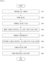
- FIG. 9 is a flowchart representing a manufacturing method of the strain sensor 1 according to one embodiment.
- the manufacturing method of the strain sensor 1 may include preparing the SOI wafer at act S10, forming holes at act S20, removing an oxide film at act S30, moving the single-crystal silicon thin film layer 110 at act S40, removing a photoresist at act S50, patterning the single-crystal silicon thin film layer (e.g., single-crystal silicon thin film layer 110) at act S60, forming the wiring part (e.g., wiring part 30) at act S70, and forming the encapsulation part (e.g., encapsulation part 40) at act S80.
- the single-crystal silicon thin film layer e.g., single-crystal silicon thin film layer 110
- the wiring part e.g., wiring part 30
- encapsulation part e.g., encapsulation part 40
- FIG. 10 is a cross-sectional view showing the SOI wafer 100 according to one embodiment.
- the silicon-on-insulator (SOI) wafer may be prepared in which the single-crystal silicon thin film layer 110, an insulating oxide film layer 120, and the base wafer layer 130 are sequentially stacked.
- the single-crystal silicon thin film layer 110 may be doped with p-type boron impurities by ion implantation at a concentration of 5e17 to 5e18 cm -3 .
- the single-crystal silicon thin film layer 110 may be formed of a silicon nanomembrane (SiNM).
- the single-crystal silicon thin film layer 110 may be a very thin and flexible single-crystal silicon thin film, and may have a nanometer-scale thickness.
- the insulating oxide film layer 120 may be formed of silicon dioxide (SiO 2 ).
- the insulating oxide film layer 120 may act as an insulator which can serve to electrically insulate and protect silicon.
- the base wafer layer 130 may be formed of silicon (Si). Silicon may be stable at high temperatures, may have high conductivity, and may have excellent optical and mechanical properties.
- the single-crystal silicon thin film layer 110 may be doped with the p-type boron impurities to provide characteristics necessary for operation of the strain sensor 1. Doping is a process of introducing atoms or ions into silicon to change the electrical properties of silicon.
- Boron is an element used to make p-type silicon.
- Ion implantation may be a process of introducing boron ions into the single-crystal silicon thin film layer 110, and here, the concentration of boron ions may be set to 5e18 cm -3 .
- the electrical properties of silicon may be changed by introducing boron ions into silicon.
- the doped silicon may be p-type silicon having increased conductivity, and may obtain a necessary gauge factor if the doped silicon is operated as the strain gauge 20 of the strain sensor 1.
- a process of adjusting the electrical characteristics of the strain sensor 1 may be carried out by doping the single-crystal silicon thin film layer 110 with boron impurities through ion implantation.
- FIG. 11 is a cross-sectional view showing a state in which a hole pattern 150 is formed in the single-crystal silicon thin film layer 110 according to one embodiment.
- forming the holes e.g., at act S20
- Forming the holes may include stacking a photoresist (PR) 170 on the single-crystal silicon thin film layer 110, forming the hole pattern 150, and dry-etching the single-crystal silicon thin film layer 110.
- the thickness of the photoresist 170 may be 300 to 600 nm.
- the photoresist 170 may be a light-sensitive material, and may be used in semiconductor manufacturing and mask manufacturing processes.
- the photoresist 170 may be used to form a predefined pattern in the photolithography process.
- the hole pattern 150 having microholes with a micrometer-scale diameter may be obtained through the photolithography process.
- the microholes may be formed by patterning the photoresist having a thickness of 300 nm to 600 nm and then piercing the single-crystal silicon thin film layer 110 in a corresponding pattern through a reactive ion etching process.
- the microholes having a diameter of 3 ⁇ m may be arranged at intervals of 50 ⁇ m.
- the hole pattern 150 may include the microholes having a micrometer-scale diameter, and may be an element configured to form the strain gauge 20 of the strain sensor 1.
- the photoresist 170 used to form the hole pattern 150 may cause a chemical reaction in portions thereof exposed to light, and may form the desired hole pattern 150.
- the photoresist 170 may serve as a cushioning material configured to prevent cracks which may occur in the single-crystal silicon thin film layer 110, the photoresist 170 may be left without being removed even after the photolithography process.
- the hole pattern 150 may be first formed in the photoresist 170, and then, the hole pattern 150 may also be formed in the single-crystal silicon thin film layer 110 through etching.
- the single-crystal silicon thin film layer 110 exposed through the hole pattern 150 may be dry-etched using a reactive ion etching (RIE) process.
- the RIE process may be a process of removing a material using reactive ions, and silicon in areas exposed through the hole pattern 150 may be removed by etching. Silicon may be removed from portions of the single-crystal silicon thin film layer 110 exposed through the hole pattern 150 by etching through the RIE process.
- the insulating oxide film layer 120 below the single-crystal silicon thin film layer 110 may be exposed. If the single-crystal silicon thin film layer 110 is exposed after dry-etching, removing the oxide film (e.g., at act S30) may be performed.
- FIG. 12 is a cross-sectional view showing a state in which the insulating oxide film layer 120 is removed from the SOI wafer 100 according to one embodiment. As shown in FIG. 12 , in removing the oxide film (e.g., at act S30), the insulating oxide film layer 120 may be removed from the SOI wafer 100.
- the insulating oxide film layer 120 may be removed by placing the SOI wafer 100 provided with the hole pattern 150 formed thereon in a hydrofluoric acid solution.
- the insulating oxide film layer 120 may be wet-etched by soaking the SOI wafer 100 on which the microholes are patterned in the hydrofluoric acid solution for about 20 minutes, and thereby, the single-crystal silicon thin film layer 110 having a thickness of 300 nm may be separated from the base wafer layer 130.
- Hydrofluoric acid may be an acidic solution used in the wet etching process, and may interact with the insulating oxide film layer 120 to remove the insulating oxide film layer 120.
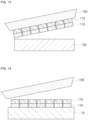
- FIG. 13 is a cross-sectional view showing a state in which a PDMS stamp 190, according to one embodiment, lifts the single-crystal silicon thin film layer 110 and the photoresist 170 above the base wafer layer 130.
- FIG. 14 is a cross-sectional view showing a state in which the PDMS stamp 190, according to one embodiment, places the single-crystal silicon thin film layer 110 and the photoresist 170 on the backing part 10.
- the single-crystal silicon thin film layer 110 may be moved from the base wafer layer 130 to the backing part 10.
- Moving the single-crystal silicon thin film layer 110 may include separating the single-crystal silicon thin film layer 110 from the base wafer layer 130, coating the backing part 10 with liquid polyimide and then soft-baking the backing part 10, and transferring the single-crystal silicon thin film layer 110 to the backing part 10 after soft-baking.
- the PDMS stamp 190 may be a type of elastomer stamp.
- the elastomer stamp may be a flexible and elastic stamp formed of an elastomer material, and may be mainly used for nanopattern and micropattern transfer, printing, adhesion, and the like.
- the PDMS stamp 190 may be a stamp formed of a flexible and transparent silicone-based rubber material.
- PDMS may be biologically safe and may be used in various application fields due to resistance and elasticity thereof.
- the PDMS stamp 190 may be a stamp manufactured using polydimethylsiloxane, which is a silicone-based elastomer, and may transfer the single-crystal silicon thin film layer 110 from the base wafer layer 130 to the backing part 10 according to one embodiment.
- the PDMS stamp 190 may be manufactured by mixing a PDMS base and a curing agent in a ratio of 4:1, and curing the mixture in an oven at a temperature of 40 °C for 24 hours.
- the PDMS stamp 190 may have flexibility to be bent and deformed into various shapes because PDMS is flexible and elastic. Further, the PDMS stamp 190 may have excellent adhesion to other surfaces. Thereby, the PDMS stamp 190 may be used to accurately transfer or attach a desired pattern.
- the backing part 10 formed of the polyimide film may be spin-coated with liquid polyimide, and may then be soft-baked.
- soft-baking curing may be performed at a temperature of 100 to 110 °C for 30 to 50 seconds.
- the backing part 10 may be coated with a liquid adhesive polymer having a thickness of 1 to 25 ⁇ m or more, and may then be cured in a heater at a temperature of 110 °C for 30 to 50 seconds.
- the liquid adhesive polymer may be one of polyimide, polyurethane, and/or epoxy.
- the backing part 10 such as formed of a polyimide film of a thickness of 25 ⁇ m, may be spin-coated with liquid polyimide.
- Spin coating is a process of applying a liquid material to a rotating substrate or wafer at a constant speed.
- the backing part 10 may be soft-baked.
- liquid polyimide spin-coated on the backing part 10 may be heated to an appropriate temperature to remove a portion of a solvent. In this process, adhesive strength of polyimide becomes stronger than that of the PDMS stamp 190.
- the single-crystal silicon thin film layer 110 separated by the PDMS stamp 190 may be transferred to the backing part 10 in which soft-baking has been completed. Because the adhesive strength of the soft-baked liquid polyimide may be stronger than the adhesive strength of the PDMS stamp 190, transfer of the single-crystal silicon thin film layer 110 may be carried out.
- the single-crystal silicon thin film layer 110 separated by the PDMS stamp 190 may be transferred to the backing part 10 in which soft-baking has been completed.
- the soft-baked liquid polyimide may have stronger adhesion to single-crystal silicon, and make transfer of single-crystal silicon thin film layer 110 to the backing part 10 possible.
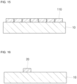
- FIG. 15 is a cross-sectional view showing a state in which only the single-crystal silicon thin film layer 110 is placed on the backing part 10 according to one embodiment. As shown in FIG. 15 , in removing the photoresist 170 (e.g., at act S50), the photoresist 170 remaining on the single-crystal silicon thin film layer 110 may be removed.
- the photoresist 170 remaining on the single-crystal silicon thin film layer 110 may be removed using acetone.
- the photoresist 170 may be a light-sensitive material used for masking or pattern formation.
- the surface of the single-crystal silicon thin film layer 110 may be cleaned by removing the photoresist 170 therefrom.
- Acetone which is a generally used solvent, may be effective in dissolving the photoresist 170.
- the backing part 10 to which the single-crystal silicon thin film layer 110 is transferred may be hard-baked.
- polyimide may be heated to an appropriate temperature so that the solvent may be removed and polyimide may be converted to a solid state. Hard-baked polyimide may form a stable bond with single-crystal silicon and reinforce the structure of the strain sensor 1.
- curing may be performed at a temperature of 195 to 205 °C for 2 hours.
- the liquid adhesive polymer may be cured in an oven at a temperature of 200 °C for 2 hours.
- the photoresist 170 remaining on the transferred single-crystal silicon thin film layer 110 may be removed, and liquid polyimide may be hard-baked to ensure stability.
- FIG. 16 is a cross-sectional view showing a state in which the strain gauge 20 formed by patterning the single-crystal silicon thin film layer 110 (e.g., at act S60) is placed on the backing part 10 according to one embodiment.
- the strain gauge 20 may be formed in the single-crystal silicon thin film layer 10 using masking and etching processes.
- Patterning may refer to a process of procedurally forming a pattern on a surface or a material so as to create a desired pattern, and may be a term mainly used in the semiconductor manufacturing process.
- Patterning the single-crystal silicon thin film layer 110 may include applying the photolithography process to the single-crystal silicon thin film layer 110, and forming the strain gauge 20 by dry-etching the single-crystal silicon thin film layer 110.
- the photolithography process is a process of using a light-sensitive material (e.g., the photoresist 170) to form a predetermined pattern.
- the photoresist 170 may be patterned into a desired shape through UV exposure.
- the shape of the patterned photoresist 170 may be a zigzag shape or a serpentine shape.
- the strain gauge 20 may be formed by dry-etching the single-crystal silicon thin film layer 110 into the zigzag shape or the serpentine shape using the reactive ion etching (RIE) process.
- RIE reactive ion etching
- Reactive ion etching is a method of etching a silicon surface using ionized particles by generating plasma.
- the serpentine shape may be formed by partially etching single-crystal silicon using the patterned photoresist 170 as a mask.
- the serpentine-shaped pattern may be obtained by removing parts of the single-crystal silicon thin film layer 110.
- the serpentine structure may be designed with a certain twisted pattern so as to allow the strain gauge 20 to detect tension in the x-axis and y-axis directions.
- the initial resistance of the strain sensor 1 may be adjusted through the above patterning process.
- the initial resistance value of the strain sensor 1 may be controlled by adjusting the overall length and thickness of the serpentine structure.
- FIG. 17 is a cross-sectional view showing a state in which the wiring part 30 is in ohmic contact with the strain gauge 21 according to one embodiment.
- forming the wiring part 30 e.g., at act S70 is a process of depositing a metal film 180 used as the wiring part 30 on the exterior of the backing part 10 and forming the wiring part 30 through the photolithography process.
- the wiring part 30 which is the metal wiring, may provide electrical connection between the strain sensor 1 and an external system.
- the wiring part 30 may be mainly formed of copper or other highly conductive metals.
- the metal film 180 may include at least one of copper, aluminum, gold, or silver.
- the metal wiring may be formed through a copper film deposition process.
- Copper is one of the metal materials generally used in strain sensors due to excellent conductivity and low price.
- the copper film may be deposited on the exterior of the backing part 10 using deposition equipment, and may be electrically connected to the strain gauge 20.
- a pattern of the metal wiring may be formed through the photolithography process.
- a desired pattern may be formed using a light-sensitive material (e.g., photoresist 170).
- the photoresist 170 may be patterned to determine the position of the wiring part 30 through UV exposure.
- a desired metal wiring pattern may be formed by etching the copper film using the photoresist 170 patterned through the photolithography process as a mask.
- the copper film may be partially etched through an etching process. If the etching process is performed using the patterned photoresist 170 as a mask, only portions of the copper film protected by the mask may remain to form the wiring part 30.
- FIG. 18 is a cross-sectional view showing a state in which the encapsulation part 40 is formed on the backing part 10 while surrounding the strain gauge 20 and the wiring part 30 according to at least one embodiment.
- the encapsulation part 40 in forming the encapsulation part 40 (e.g., at act S80), the encapsulation part 40 may be formed on the backing part 10 while surrounding the strain gauge 20 and the wiring part 30.
- the encapsulation part 40 may be formed along with formation of the wiring connection hole 42 configured to expose a portion of the wiring part 30 for connection to external wiring.
- the encapsulation part 40 may be formed of SU-8, which is the epoxy-based resin having the Young's modulus similar to that of polyimide.
- Polyimide may have excellent heat resistance and durability, and may serve to protect the strain sensor 1 and provide stability of the strain sensor 1.
- Coating of polyimide or SU-8 and patterning thereof may be achieved through the photolithography process.
- a desired pattern may be formed using a mask, and the pattern may be produced through exposure and post-processing.
- the encapsulation part 40 may serve to protect the strain sensor 1 from external shock and environmental factors and to secure stability of the strain sensor 1.
- Forming the encapsulation part 40 may include stacking epoxy on the backing part 10 while surrounding the strain gauge 20 and the wiring part 30, and processing the epoxy stacked on the backing part 10 into the shape of the encapsulation part 40 through the photolithography process to expose the portion of the wiring part 30.
- the encapsulation part 40 may be manufactured using various polymer materials.
- polymer materials such as silicone, polyurethane, epoxy resins, and the like, may be used. These polymer materials may be inexpensive and readily available, and may provide various physical and chemical properties.
- FIG. 4 is a side view showing the secondary battery 200 equipped with the strain sensor 1 according to one embodiment.
- FIG. 5 is a side view showing a state in which the strain sensor 1 is bent, as the case 210 expands, according to one embodiment.
- the strain sensor 1 may be mounted on the exterior of the case 210.
- the case 210 surrounding the exterior of an electrode assembly 220 may have various shapes.
- the case 210 may have one of a hexahedral shape, a cylindrical shape, and/or a pouch shape.
- a pouch-type case 210 will be described as an example.
- the strain sensor 1 may be attached to the exterior of the case 210 and may measure deformation of the case 210.
- the strain sensor 1 may include the strain gauge 20 formed of single-crystal silicon. The detailed configuration and manufacturing method of the strain sensor 1, having been described above with a detailed description thereof, will thus be omitted for simplicity.
- FIG. 5 shows a mechanism to detect occurrence of swelling of the secondary battery 200 after attaching the strain sensor 1, according to one embodiment, to the pouch-type case 210.
- the length of the strain gauge 20 in an initial state in which swelling of the secondary battery 200 does not occur may be L0. In this state, if swelling occurs in the secondary battery 200, the strain sensor 1 attached to the exterior of the case 210 is in a bent state, and the upper portion of the strain sensor 1 may undergo tensile strain while the lower portion of the strain sensor 1 may undergo compressive strain, based on the boundary layer 14, which is the neutral mechanical plane.
- the thickness of the backing part 10 may be more than 10 or more times that of the encapsulation part 40.
- the strain gauge 20 may be located at the upper end of the strain sensor 1, and may undergo tensile strain so that resistance may be increased, if swelling of the secondary battery 200 occurs.
- the backing part may be attached to the exterior of the case, in some examples.
- strain may be proportional to a distance from the neutral mechanical plane compared to the overall thickness of the strain sensor 1, without wishing to be bound by any particular theory, the sensitivity and physical stability of the strain sensor 1 may be controlled by adjusting the thicknesses of the backing part 10 and the encapsulation part 40.
- first deformation layer 12, the boundary layer 14, and the second deformation layer 16 in the backing part 10 having a greater thickness than that of the encapsulation part 40 has been described; yet, the first deformation layer 12, the boundary layer 14, and the second deformation layer 16 may be formed throughout the total height of the strain sensor 1 including the encapsulation part 40 and the backing part 10.
- FIG. 6 is a perspective view showing the strain sensor 1 installed on the exterior of the expanded case 210 according to one embodiment. As shown in FIG. 6 , the strain sensor 1 may be attached to the exterior of the pouch-type case 210 to detect swelling of the secondary battery 200.
- the strain sensor 1 may be attached to the upper end of the pouch-type case 210 using an acrylic adhesive. Unlike silicone-based adhesives used in tapes, acrylic adhesives may be thin and have high strength. Therefore, if the strain sensor 1 is attached to the secondary battery 200, the acrylic adhesive may be smoothly deformed depending on deformation of the secondary battery 200, thereby reducing hysteresis of a measured value caused by repetitive bending.
- the acrylic adhesive may be adhered to the strain sensor 1 more strongly and to a thinner thickness, and may thus follow the deformation of the secondary battery 200 well and serve to improve performance of the strain sensor 1.
- the pouch-type case 210 may not be deformed into an arc shape, but may be deformed into a plateau shape where the sides are bent more than the center. Therefore, the strain sensor 1 may be attached to a side part of the pouch-type case 210 rather than the central part thereof, and thus, more strain may be transmitted to the strain sensor 1 if swelling occurs.
- the attachment position of the strain sensor may be set to the side part rather than the center of the case 210 to more accurately measure a strain value, if the case 210 of the secondary battery 200 is deformed due to the swelling phenomenon.
- FIG. 8 is a graph representing the resistance value ( ⁇ ) of the strain sensor 1 over time if the strain sensor 1, according to one embodiment, detects a swelling phenomenon. As shown in FIG. 8 , point A may represent the resistance of the strain sensor 1 immediately after attaching the strain sensor 1 to the case 210 at the beginning of an experiment.
- Section A-B may show that the resistance of the strain sensor 1 increases due to an increase in strain applied to the strain sensor 1 due to swelling of the secondary battery 200 up to 32 hours after leaving the secondary battery 200 in a high-temperature chamber.
- Point B may be a point at which rapid swelling begins to occur after 32 hours of leaving the secondary battery 200 at high temperatures, showing an increase in strain applied to the strain sensor 1, e.g., an increase in the resistance of the strain sensor 1.
- Section B-C may show an increase in the resistance of the strain sensor 1 until swelling of 140% occurs based on the thickness after rapid swelling has occurred.
- Point C may represent the resistance of the strain sensor 1 at a point in time when swelling is finished after 75 hours.
- the resistance of single-crystal silicon may be changed due to changes in temperature in addition to changes in the applied strain, but this experiment was conducted in the chamber maintained at a high temperature of 85 °C so that temperature dependence was excluded and only the resistance change due to swelling of the secondary battery 200 was confirmed.
- the strain sensor 1 may detect a slight swelling phenomenon of the secondary battery 200 which may not be confirmed by the existing metal-based strain gauges having a low gauge factor. Therefore, the strain sensor 1 may inform a user of the risk of battery explosion so as to prevent the risk of explosion and fire.
- embodiments may prevent explosion and fire of a secondary battery by detecting deformation of a case of the secondary battery due to a swelling phenomenon of the secondary battery.
- embodiments may respond sensitively to slight deformation using a single-crystal silicon-based strain gauge, thereby being capable of improving accuracy in measurement.
- a method of manufacturing a strain sensor including: preparing a silicon-on-insulator (SOI) wafer configured such that a single-crystal silicon thin film layer, an insulating oxide film layer, and a base wafer layer are sequentially stacked; forming holes by forming a hole pattern in the single-crystal silicon thin film layer using a photolithography process; removing an oxide film by removing the insulating oxide film layer from the SOI wafer; moving the single-crystal silicon thin film layer from the base wafer layer to a backing part; removing a photoresist remaining on the single-crystal silicon thin film layer; patterning the single-crystal silicon thin film layer to form a strain gauge using masking and etching processes; forming a wiring part by depositing a metal film configured to be the wiring part on an exterior of the backing part and by performing the photolithography process; and forming an encapsulation part on the backing part configured to surround the strain gauge
- the single-crystal silicon thin film layer may be doped with p-type boron impurities by ion implantation at a concentration of 5e 17 to 5e18 cm -3 .
- forming the holes may include: stacking the photoresist on the single-crystal silicon thin film layer; forming the hole pattern including microholes with a micrometer-scale diameter by using a light source; and dry-etching the single-crystal silicon thin film layer exposed through the hole pattern by using a reactive ion etching (RIE) process.
- RIE reactive ion etching
- a thickness of the photoresist may be 300 to 600 nm.
- the hole pattern may be configured such that the microholes have a diameter of 3 ⁇ m and are arranged at intervals of 50 ⁇ m.
- the insulating oxide film layer may be removed by putting the SOI wafer provided with the hole pattern formed thereon into a hydrofluoric acid solution.
- moving the single-crystal silicon thin film layer may include: separating the single-crystal silicon thin film layer from the base wafer layer using a polydimethylsiloxane (PDMS) stamp; spin-coating the backing part formed of a polyimide film with liquid polyimide, and after the spin-coating, soft-baking the backing part; and transferring the single-crystal silicon thin film layer separated by the PDMS stamp to the backing part after the soft-baking.
- PDMS polydimethylsiloxane
- removing the photoresist may include: removing the photoresist using acetone and hard-baking the backing part provided with the single-crystal silicon thin film layer transferred thereto after removing the photoresist.
- curing may be performed at a temperature of 100 to 110 °C for 30 to 50 seconds
- curing may be performed at a temperature of 195 to 205 ° C for 2 hours.
- Patterning the single-crystal silicon thin film layer may include: applying the photolithography process to the single-crystal silicon thin film layer; and forming the strain gauge by dry-etching the single-crystal silicon thin film layer into a zigzag shape or a serpentine shape using a reactive ion etching (RIE) process.
- the metal film may include at least one of copper, aluminum, gold, or silver.
- Forming the encapsulation part may include: stacking epoxy on the backing part configured to surround the strain gauge (e.g., strain gauge 20) and the wiring part; and processing the epoxy stacked on the backing part into a shape of the encapsulation part through the photolithography process to expose a portion of the wiring part.
Landscapes
- Physics & Mathematics (AREA)
- General Physics & Mathematics (AREA)
- Chemical & Material Sciences (AREA)
- Engineering & Computer Science (AREA)
- Manufacturing & Machinery (AREA)
- Chemical Kinetics & Catalysis (AREA)
- Electrochemistry (AREA)
- General Chemical & Material Sciences (AREA)
- Analytical Chemistry (AREA)
- Microelectronics & Electronic Packaging (AREA)
- Measurement Of Length, Angles, Or The Like Using Electric Or Magnetic Means (AREA)
Applications Claiming Priority (1)
| Application Number | Priority Date | Filing Date | Title |
|---|---|---|---|
| KR1020230128898A KR20250045682A (ko) | 2023-09-26 | 2023-09-26 | 스트레인 센서, 스트레인 센서의 제조방법 및 스트레인 센서가 장착된 이차전지 |
Publications (1)
| Publication Number | Publication Date |
|---|---|
| EP4530591A1 true EP4530591A1 (fr) | 2025-04-02 |
Family
ID=92409198
Family Applications (1)
| Application Number | Title | Priority Date | Filing Date |
|---|---|---|---|
| EP24194387.7A Pending EP4530591A1 (fr) | 2023-09-26 | 2024-08-13 | Capteur de contrainte, procédé de fabrication de capteur de contrainte et batterie secondaire équipée d'un capteur de contrainte |
Country Status (3)
| Country | Link |
|---|---|
| US (1) | US20250102286A1 (fr) |
| EP (1) | EP4530591A1 (fr) |
| KR (1) | KR20250045682A (fr) |
Citations (3)
| Publication number | Priority date | Publication date | Assignee | Title |
|---|---|---|---|---|
| US20110226069A1 (en) * | 2010-03-18 | 2011-09-22 | Korea Research Institute Of Standards And Science | Flexible force or pressure sensor array using semiconductor strain gauge, fabrication method thereof and measurement method thereof |
| US20160250015A1 (en) * | 2015-02-27 | 2016-09-01 | Seoul National University R&Db Foundation | Stretchable electronics for artificial skin |
| CN112913068A (zh) * | 2018-08-28 | 2021-06-04 | 美蓓亚三美株式会社 | 电池组 |
-
2023
- 2023-09-26 KR KR1020230128898A patent/KR20250045682A/ko active Pending
-
2024
- 2024-08-13 EP EP24194387.7A patent/EP4530591A1/fr active Pending
- 2024-09-09 US US18/828,609 patent/US20250102286A1/en active Pending
Patent Citations (3)
| Publication number | Priority date | Publication date | Assignee | Title |
|---|---|---|---|---|
| US20110226069A1 (en) * | 2010-03-18 | 2011-09-22 | Korea Research Institute Of Standards And Science | Flexible force or pressure sensor array using semiconductor strain gauge, fabrication method thereof and measurement method thereof |
| US20160250015A1 (en) * | 2015-02-27 | 2016-09-01 | Seoul National University R&Db Foundation | Stretchable electronics for artificial skin |
| CN112913068A (zh) * | 2018-08-28 | 2021-06-04 | 美蓓亚三美株式会社 | 电池组 |
Also Published As
| Publication number | Publication date |
|---|---|
| US20250102286A1 (en) | 2025-03-27 |
| KR20250045682A (ko) | 2025-04-02 |
Similar Documents
| Publication | Publication Date | Title |
|---|---|---|
| US7992447B2 (en) | Miniature sensor | |
| WO2017028466A1 (fr) | Puce de jauge de contrainte mems et son procédé de fabrication | |
| EP1861687B1 (fr) | Capteur de pression polymérique avec des régions piézorésistives implantées | |
| JP5470533B2 (ja) | 触覚センサおよびそれを備えたロボット | |
| US8511171B2 (en) | Device for measuring environmental forces and method of fabricating the same | |
| CN110057475B (zh) | 一种高灵敏度石墨烯压阻式应变传感器 | |
| CN110174197A (zh) | 石墨烯基压阻式压力传感器及其制备方法 | |
| Zhou et al. | Flexible substrate micro-crystalline silicon and gated amorphous silicon strain sensors | |
| CN102998345A (zh) | 环境传感器 | |
| CN113567869B (zh) | 一种电池电压监测微型传感器及电压监测方法 | |
| KR20090081195A (ko) | 금속 압력다이어프램이 구비된 압력측정센서 및 상기압력측정센서의 제조방법 | |
| WO2021023251A1 (fr) | Structure mems, procédé de fabrication de structure mems, et capteur de pression de pneu | |
| CN112573477B (zh) | 基于静电力和压阻效应的微型电场传感器件的制备工艺流程 | |
| KR102556903B1 (ko) | 대면적 맥신 전극 패턴의 전사에 의한 유연 마이크로 슈퍼캐패시터 소자 제조 방법 | |
| CN102976263B (zh) | 一种mems压阻式多轴力传感器的制备方法 | |
| EP4530591A1 (fr) | Capteur de contrainte, procédé de fabrication de capteur de contrainte et batterie secondaire équipée d'un capteur de contrainte | |
| CN111722707B (zh) | 一种背接触触觉传感器的制作方法及背接触触觉传感器 | |
| CN116878702A (zh) | 抗电磁干扰的mems压阻式压力传感器及其制备方法 | |
| CN111397776B (zh) | 一种温压复合传感器 | |
| CN111351607B (zh) | 一种温压复合传感器的制作方法 | |
| CN111017863A (zh) | 一种硅基网状石墨烯mems传感器及其制备方法 | |
| JP2003166998A (ja) | 半導体加速度センサ | |
| CN102419283B (zh) | 微型拉伸测量组件及其制作方法 | |
| CN114955980A (zh) | 基于pdms-硅纳米膜的柔性心音传感器及其制备方法 | |
| CN118125373B (zh) | 氢气传感器的制备方法及氢气传感器 |
Legal Events
| Date | Code | Title | Description |
|---|---|---|---|
| PUAI | Public reference made under article 153(3) epc to a published international application that has entered the european phase |
Free format text: ORIGINAL CODE: 0009012 |
|
| STAA | Information on the status of an ep patent application or granted ep patent |
Free format text: STATUS: REQUEST FOR EXAMINATION WAS MADE |
|
| 17P | Request for examination filed |
Effective date: 20240813 |
|
| AK | Designated contracting states |
Kind code of ref document: A1 Designated state(s): AL AT BE BG CH CY CZ DE DK EE ES FI FR GB GR HR HU IE IS IT LI LT LU LV MC ME MK MT NL NO PL PT RO RS SE SI SK SM TR |
|
| STAA | Information on the status of an ep patent application or granted ep patent |
Free format text: STATUS: EXAMINATION IS IN PROGRESS |
|
| 17Q | First examination report despatched |
Effective date: 20250917 |
|
| GRAP | Despatch of communication of intention to grant a patent |
Free format text: ORIGINAL CODE: EPIDOSNIGR1 |
|
| STAA | Information on the status of an ep patent application or granted ep patent |
Free format text: STATUS: GRANT OF PATENT IS INTENDED |
|
| INTG | Intention to grant announced |
Effective date: 20251209 |
|
| GRAS | Grant fee paid |
Free format text: ORIGINAL CODE: EPIDOSNIGR3 |
|
| GRAA | (expected) grant |
Free format text: ORIGINAL CODE: 0009210 |
|
| STAA | Information on the status of an ep patent application or granted ep patent |
Free format text: STATUS: THE PATENT HAS BEEN GRANTED |