EP4528811A1 - Dispositif semi-conducteur encapsulé et procédé de fabrication - Google Patents
Dispositif semi-conducteur encapsulé et procédé de fabrication Download PDFInfo
- Publication number
- EP4528811A1 EP4528811A1 EP24194545.0A EP24194545A EP4528811A1 EP 4528811 A1 EP4528811 A1 EP 4528811A1 EP 24194545 A EP24194545 A EP 24194545A EP 4528811 A1 EP4528811 A1 EP 4528811A1
- Authority
- EP
- European Patent Office
- Prior art keywords
- semiconductor device
- perimeter
- packaged semiconductor
- landings
- device die
- Prior art date
- Legal status (The legal status is an assumption and is not a legal conclusion. Google has not performed a legal analysis and makes no representation as to the accuracy of the status listed.)
- Pending
Links
Images


Classifications
-
- H—ELECTRICITY
- H10—SEMICONDUCTOR DEVICES; ELECTRIC SOLID-STATE DEVICES NOT OTHERWISE PROVIDED FOR
- H10W—GENERIC PACKAGES, INTERCONNECTIONS, CONNECTORS OR OTHER CONSTRUCTIONAL DETAILS OF DEVICES COVERED BY CLASS H10
- H10W70/00—Package substrates; Interposers; Redistribution layers [RDL]
- H10W70/40—Leadframes
- H10W70/421—Shapes or dispositions
- H10W70/438—Shapes or dispositions of side rails, e.g. having holes
-
- H—ELECTRICITY
- H10—SEMICONDUCTOR DEVICES; ELECTRIC SOLID-STATE DEVICES NOT OTHERWISE PROVIDED FOR
- H10W—GENERIC PACKAGES, INTERCONNECTIONS, CONNECTORS OR OTHER CONSTRUCTIONAL DETAILS OF DEVICES COVERED BY CLASS H10
- H10W70/00—Package substrates; Interposers; Redistribution layers [RDL]
- H10W70/40—Leadframes
- H10W70/479—Leadframes on or in insulating or insulated package substrates, interposers, or redistribution layers
-
- H—ELECTRICITY
- H10—SEMICONDUCTOR DEVICES; ELECTRIC SOLID-STATE DEVICES NOT OTHERWISE PROVIDED FOR
- H10W—GENERIC PACKAGES, INTERCONNECTIONS, CONNECTORS OR OTHER CONSTRUCTIONAL DETAILS OF DEVICES COVERED BY CLASS H10
- H10W70/00—Package substrates; Interposers; Redistribution layers [RDL]
- H10W70/40—Leadframes
- H10W70/421—Shapes or dispositions
- H10W70/424—Cross-sectional shapes
-
- H—ELECTRICITY
- H10—SEMICONDUCTOR DEVICES; ELECTRIC SOLID-STATE DEVICES NOT OTHERWISE PROVIDED FOR
- H10P—GENERIC PROCESSES OR APPARATUS FOR THE MANUFACTURE OR TREATMENT OF DEVICES COVERED BY CLASS H10
- H10P72/00—Handling or holding of wafers, substrates or devices during manufacture or treatment thereof
- H10P72/70—Handling or holding of wafers, substrates or devices during manufacture or treatment thereof for supporting or gripping
- H10P72/74—Handling or holding of wafers, substrates or devices during manufacture or treatment thereof for supporting or gripping using temporarily an auxiliary support
-
- H—ELECTRICITY
- H10—SEMICONDUCTOR DEVICES; ELECTRIC SOLID-STATE DEVICES NOT OTHERWISE PROVIDED FOR
- H10W—GENERIC PACKAGES, INTERCONNECTIONS, CONNECTORS OR OTHER CONSTRUCTIONAL DETAILS OF DEVICES COVERED BY CLASS H10
- H10W70/00—Package substrates; Interposers; Redistribution layers [RDL]
- H10W70/01—Manufacture or treatment
- H10W70/04—Manufacture or treatment of leadframes
-
- H—ELECTRICITY
- H10—SEMICONDUCTOR DEVICES; ELECTRIC SOLID-STATE DEVICES NOT OTHERWISE PROVIDED FOR
- H10W—GENERIC PACKAGES, INTERCONNECTIONS, CONNECTORS OR OTHER CONSTRUCTIONAL DETAILS OF DEVICES COVERED BY CLASS H10
- H10W70/00—Package substrates; Interposers; Redistribution layers [RDL]
- H10W70/01—Manufacture or treatment
- H10W70/05—Manufacture or treatment of insulating or insulated package substrates, or of interposers, or of redistribution layers
- H10W70/08—Manufacture or treatment of insulating or insulated package substrates, or of interposers, or of redistribution layers by depositing layers on the chip or wafer, e.g. "chip-first" RDLs
- H10W70/09—Manufacture or treatment of insulating or insulated package substrates, or of interposers, or of redistribution layers by depositing layers on the chip or wafer, e.g. "chip-first" RDLs extending onto an encapsulation that laterally surrounds the chip or wafer, e.g. fan-out wafer level package [FOWLP] RDLs
-
- H—ELECTRICITY
- H10—SEMICONDUCTOR DEVICES; ELECTRIC SOLID-STATE DEVICES NOT OTHERWISE PROVIDED FOR
- H10W—GENERIC PACKAGES, INTERCONNECTIONS, CONNECTORS OR OTHER CONSTRUCTIONAL DETAILS OF DEVICES COVERED BY CLASS H10
- H10W70/00—Package substrates; Interposers; Redistribution layers [RDL]
- H10W70/01—Manufacture or treatment
- H10W70/05—Manufacture or treatment of insulating or insulated package substrates, or of interposers, or of redistribution layers
- H10W70/098—Applying pastes or inks, e.g. screen printing
-
- H—ELECTRICITY
- H10—SEMICONDUCTOR DEVICES; ELECTRIC SOLID-STATE DEVICES NOT OTHERWISE PROVIDED FOR
- H10W—GENERIC PACKAGES, INTERCONNECTIONS, CONNECTORS OR OTHER CONSTRUCTIONAL DETAILS OF DEVICES COVERED BY CLASS H10
- H10W70/00—Package substrates; Interposers; Redistribution layers [RDL]
- H10W70/60—Insulating or insulated package substrates; Interposers; Redistribution layers
-
- H—ELECTRICITY
- H10—SEMICONDUCTOR DEVICES; ELECTRIC SOLID-STATE DEVICES NOT OTHERWISE PROVIDED FOR
- H10W—GENERIC PACKAGES, INTERCONNECTIONS, CONNECTORS OR OTHER CONSTRUCTIONAL DETAILS OF DEVICES COVERED BY CLASS H10
- H10W74/00—Encapsulations, e.g. protective coatings
- H10W74/01—Manufacture or treatment
- H10W74/014—Manufacture or treatment using batch processing
-
- H—ELECTRICITY
- H10—SEMICONDUCTOR DEVICES; ELECTRIC SOLID-STATE DEVICES NOT OTHERWISE PROVIDED FOR
- H10W—GENERIC PACKAGES, INTERCONNECTIONS, CONNECTORS OR OTHER CONSTRUCTIONAL DETAILS OF DEVICES COVERED BY CLASS H10
- H10W74/00—Encapsulations, e.g. protective coatings
- H10W74/10—Encapsulations, e.g. protective coatings characterised by their shape or disposition
- H10W74/111—Encapsulations, e.g. protective coatings characterised by their shape or disposition the semiconductor body being completely enclosed
- H10W74/121—Encapsulations, e.g. protective coatings characterised by their shape or disposition the semiconductor body being completely enclosed by multiple encapsulations, e.g. by a thin protective coating and a thick encapsulation
-
- H—ELECTRICITY
- H10—SEMICONDUCTOR DEVICES; ELECTRIC SOLID-STATE DEVICES NOT OTHERWISE PROVIDED FOR
- H10W—GENERIC PACKAGES, INTERCONNECTIONS, CONNECTORS OR OTHER CONSTRUCTIONAL DETAILS OF DEVICES COVERED BY CLASS H10
- H10W72/00—Interconnections or connectors in packages
- H10W72/01—Manufacture or treatment
- H10W72/0198—Manufacture or treatment batch processes
-
- H—ELECTRICITY
- H10—SEMICONDUCTOR DEVICES; ELECTRIC SOLID-STATE DEVICES NOT OTHERWISE PROVIDED FOR
- H10W—GENERIC PACKAGES, INTERCONNECTIONS, CONNECTORS OR OTHER CONSTRUCTIONAL DETAILS OF DEVICES COVERED BY CLASS H10
- H10W90/00—Package configurations
- H10W90/701—Package configurations characterised by the relative positions of pads or connectors relative to package parts
- H10W90/751—Package configurations characterised by the relative positions of pads or connectors relative to package parts of bond wires
- H10W90/755—Package configurations characterised by the relative positions of pads or connectors relative to package parts of bond wires between a chip and a laterally-adjacent insulating package substrate, interpose or RDL
Definitions
- the present disclosure relates to a packaged semiconductor device and a method of manufacturing the packaged semiconductor device.
- Quad flat no lead (“QFN”) packaged devices have compact sizes because the perimeter landings on the bottom surface are defined within the outline of the package.
- a QFN packaged device is manufactured by placing and connecting a chip die to a lead-frame, and molding the connected assembly. QFN and similar packaged devices have requirements of becoming more compact.
- a packaged semiconductor device has a top surface and a bottom surface opposite the top surface.
- the packaged semiconductor device includes a device die, a plurality of perimeter landings, connection lines, and molding compound.
- the device die has a first surface and a second surface opposite the first surface.
- the device die is arranged in a central region of the packaged semiconductor device.
- the first surface of the device die is arranged towards the bottom surface of the packaged semiconductor device, and the second surface of the device die is arranged towards the top surface of the packaged semiconductor device.
- the plurality of perimeter landings are exposed on the bottom surface of the packaged semiconductor device and are arranged at perimeter regions of the bottom surface surrounding the device die.
- the connection lines are connected to the second surface of the device die.
- connection line provides electrical connection between a corresponding connection pad on the second surface of the device die and a corresponding one of the plurality of perimeter landings.
- the molding compound at least partially encapsulates the device die and the plurality of perimeter landings.
- the plurality of perimeter landings are made of a material having a mass fraction of tin of at least 95%.
- a method of manufacturing a packaged semiconductor device includes: providing a patterned paste material having a mass fraction of tin of at least 95% on a carrier; reflowing the patterned paste material to form a plurality of arranged perimeter landings; positioning a device die on the carrier such that it is surrounded by the plurality of arranged perimeter landings; filling molding compound to integrate the perimeter landings and the device die into an integral assembly having a first surface; and forming a connection line, between a connection pad on a first surface of the device die on the first surface of the integral assembly, and a one of the plurality of arranged perimeter landings, to provide electrical connection therebetween.
- the placing the device die on the first side of the tape comprises facing a first side surface of the device die towards the tape.
- the method further comprises coating the first surface the integral assembly with a coating layer, the coating layer covering the connection line.
- the coating the first surface of the integral assembly comprises applying the coating layer to a thickness which is equal to or larger than a thickness of the connection line.
- the thickness of the connection line is in a range of 10 ⁇ m and 20 ⁇ m.
- the filling molding compound to integrate the perimeter landings and the device die into the integral assembly comprises: placing the perimeter landings and the device die into a molding cavity; and filling molding compound into the molding cavity to integrate the perimeter landings and the device die into the integral assembly.
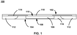
- FIG. 1 is a cross-sectional view of a packaged semiconductor device according to an embodiment.
- the packaged semiconductor device 100 has a top surface 102 and a bottom surface 104 opposite the top surface 102.
- the packaged semiconductor device 100 includes a device die 106 located in a central area of the semiconductor device 100.
- the device die 106 has a first surface 108 and a second surface 110 which is opposite the first surface 108. As can be seen from FIG. 1 , the first surface 108 of the device die 106 is arranged towards the bottom surface 104, while the second surface 110 is arranged towards the top surface 102.
- the packaged semiconductor device 100 further includes multiple perimeter landings 112 that are arranged around a perimeter of the bottom surface 104 and surrounding the device die 106.
- the thickness of the device die 106 measuring from the first surface 108 to the second surface 110, is in a range of 5 mil (0.125mm) and 15 mil (0.375mm).
- the thickness of each perimeter landing 112 can be equal to, larger than or less than the thickness of the device die 106, and is typically 80% to 100% of the thickness of the device die 106, and is further typically around 5 mil, which is about 0.125mm.
- the perimeter landings 112 are connected to the device die 106 through a corresponding connection line 114. Specifically, the connection lines 114 are attached to the second surface 110 of the device die 106.
- connection lines 114 connects a corresponding connection pad (not shown) on the second surface 110 of the device die 106 to a corresponding one of the multiple perimeter landings 112.
- the device die 106 is placed in the semiconductor device 100 such that an active area of the device die 106 faces towards the second surface 110, to provide connections to the connection lines 114 on the second surface 110.
- the connection lines 114 can be implemented as materials of copper clips that have a flat shape, etc., and have a thickness in a range of 10 ⁇ m and 20 ⁇ m.
- the packaged semiconductor device 100 further includes molding compound 116 that at least partially encapsulates the device die 106 and the perimeter landings 112.
- the molding compound 116 is electrically insulating.
- the molding compound 116 fills in gaps between the device die 106 and the perimeter landings 112, to a thickness equal to or larger than the thickness of the device die 106, such that the molding compound 116 is exposed on, and forms part of, the bottom surface 104 of the packaged semiconductor device 100.
- the second surface 110 of the device die 106 is coplanar with the surface of the molding compound 116, to allow the connection lines 114 to contact the second surface 110, which means the connection lines 114 are arranged over the molding compound 116.
- the perimeter landings 112 are made of a material having a mass fraction of tin of at least 95%. Specifically, the perimeter landings 112 are formed by printing a paste material through apertures of a stencil, and reflowing the printed paste material.
- the paste material includes tin with a high mass fraction, and has an eutectic temperature of at least 210 degree Celsius (210°C). For example, some Pb-free high-Sn paste materials have even high eutectic temperatures as high as 280°C.
- Material for the perimeter landings 112 are selected such that the eutectic temperature of the perimeter landings 112 is high enough, and will not melt when the final packaged semiconductor device 100 is mounted to a Printed Circuit Board (PCB) by Surface Mounting Technologies (SMT) in which solder paste is used for mounting the packaged semiconductor device onto the PCB and then reflowed. Solder pastes have lower eutectic temperatures than that of high-Sn pastes.
- PCB Printed Circuit Board
- SMT Surface Mounting Technologies
- the molding compound 116 of the semiconductor device 100 has a melting temperature which is lower than the eutectic temperature of the perimeter landings 112.
- the molding compound 116 of the semiconductor device 100 is selected from Epoxy Molding Compound (EMC) materials with melting temperatures around 175°C.
- the packaged semiconductor device 100 can include a coating layer 118 which is disposed over the top surface 102.
- the coating layer 118 protects the second surface 110 of the device die 106 that is exposed from the molding compound 116, the connection lines 114, and the exposing part of the perimeter landings 112, from corrosion due to oxidation, humidity, etc.
- a thickness of the coating layer 118 is at least equal to the thickness of the connection lines 114, and preferably in a range of 25 ⁇ m and 40 ⁇ m.
- the coating layer 118 can be disposed over the top surface 102 by spray painting or lacquering conformal coatings, which when cured isolates and protects the covered units.
- the packaged semiconductor device 100 includes the perimeter landings 112 that are formed by Sn pastes for providing external connections to the device die 106, instead of convention lead-frames. Because the connection lines 114 are arranged immediately adjacent the surface of the die (rather than requiring a flexure loop as is the case with convention wire bonding), the packaged semiconductor device 100 can be manufactured such that its thickness can be as compact as 0.05mm to 0.1mm.
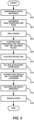
- FIG. 2 is a flow diagram of a method of manufacturing a packaged semiconductor device. The method can be implemented to manufacture the packaged semiconductor device 100 of FIG. 1 . The method will be described basing on FIG. 2 and also with references to FIGs. 3 to 14 that show cross-sectional views of parts manufactured through the steps of FIG. 2 .
- Step 202 of the method includes arranging paste material.
- paste material 302 is disposed onto a holding plate, or a carrier, 304.
- the holding plate 304 is typically a non-wetting plate, for example, a ceramic plate, or otherwise includes a release layer at its surface.
- the paste material 302 is arranged on the holding plate 304 as a patterned paste material.
- the paste material 302 is printed through apertures 306 of a stencil 308 which has been non-wetting treated.
- Known screen printing techniques may be used to dispose the paste material 302.
- the paste material 302 may be printed to a thickness equal to, or similar to, that of the stencil 308.
- the stencil 308 has a thickness of 5 mil, which is about 0.125mm.
- the stencil 308 has the thickness equal to a thickness of a device die to be placed for manufacturing the packaged semiconductor device.
- the paste material 302 in this embodiment includes tin which has a mass fraction of at least 95%, as has been described above, to have a relatively high eutectic temperature.
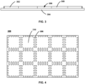
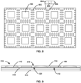
- FIG. 4 depicts a partial and plan view of the stencil 308.
- the stencil 308 has the apertures 306 that are aligned respectively along intersecting directions.
- An area 310 surrounded by the apertures 306 allows no paste material to be printed after the stencil 308 is placed on the holding plate 304, and subsequently the area 310 will be placed with a device die.
- the illustrated stencil 308 is an array of units each includes a corresponding area 310 and the surrounding apertures 306. As will be described below, each unit of the array will form a corresponding packaged semiconductor device. See from FIG. 4 that a piece of paste material 302 will be printed conformal the aperture 306.
- the piece of paste material after reflowing as described below and finally solidified, forms a region which will eventually become two perimeter landings (one for each of two die).
- the region will also include a sacrificial region that will be lost due to the width of the subsequent sawblade and kerf-loss, as will be further described below in more details.
- FIG. 5 is a cross-sectional view of the holding plate 304, the stencil 308, and the covering tape.
- the high-temperature tape 312 is adhered to the stencil 308 and the paste material 302, typically with another clamping plate 314 on the other side of the high-temperature tape 312 for applying a force to push the high-temperature tape 312 towards the stencil 308 and the paste material 302, thereby ensuring the high-temperature tape 312 reliably adheres to the paste material 302.
- Step 206 follows the step 204 of the method, to reflow the printed paste material 302.
- the assembly is heated to at least the eutectic temperature of the paste material 302.
- the holding plate 304 is heated, and accordingly heats up the paste material 302 on the holding plate 304 and in the apertures 306.
- the paste material 302 has an eutectic temperature of at least 210°C
- the reflowing step 206 heats up the paste material 302 until it is in a molten state and solvents in the paste material 302, which are relative volatile, evaporate.
- it is cooled down, melted metal elements in the paste material solidifies, and forms perimeter landings for the semiconductor device to be manufactured. It can be understood that the resulting perimeter landings are now sandwiched by the holding plate 304 and the high-temperature tape 312, and comprise mainly tin, or a high-tin fraction alloy of tin.
- the method further includes step 208, to flip the product from the previous step 206, so that the clamping plate 314, also referred to as a supporting plate, is on the bottom and supports the high-temperature tape 312, the perimeter landings 112 (similarly labelled as that in FIG. 1 ), the stencil 308, and the holding plate 304.
- the supporting plate 314 is selected to be rigid enough. Due to the flipping, the stencil 308 and the holding plate 304 are on the top, and are easy to be removed. Because the stencil 308 is non-wetting treated and the high-temperature tape 312 is adhesive, the perimeter landings 112 remain on the high-temperature tape 312.
- step 210 of the method a device die is placed onto the high-temperature tape, and is placed to be surrounded by the perimeter landings.
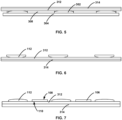
- FIG. 7 which is a cross-sectional view of the product after step 210
- FIG. 8 which is a plan view of the product after the device die is placed, as described above with reference to FIG. 4
- the device die 106 is placed in the central area 310, and surrounded by the plurality of arranged regions 802. It now can be understood that both the regions 802 and the device die 106 are arranged on a first side of the high-temperature tape 312, while the supporting plate 314 is on a second, opposite side of the high-temperature tape 312.
- the device die 106 has the first surface 108 which is away from the tape 312, and the second surface 110 which faces toward and contacts the tape 312 when the device die 106 is placed on the tape 312. Also as described above, the active area, or active layers, of the device die 106 faces towards the second surface 110.
- the region 802 is substantially oval, two ends 804 of the region 802 will become the perimeter landings respectively used for providing external connections for neighboring device die 106. A sacrificial region 806 between the ends 804 will be removed during subsequent saw blading and/or etching, shown as dotted line in FIG. 8 .
- the method further includes step 212, filling molding compound into gaps between the device die 106 and the perimeter landings 112, to integrate the perimeter landings and the device die together.
- the perimeter landings 112 and the device die 106 are placed into a molding cavity (not shown), and the molding compound 116 is filled, or injected, into the molding cavity to integrate the perimeter landings 112 and the device die 106 into an integral assembly 316 which includes the perimeter landings 112, the device die 106, and the filled molding compound 116.
- the integral assembly 316 has a first, top, surface 318 and a second, bottom, surface 320.
- the second surface 320 contacts the high-temperature tape 312.
- the molding compound 116 should be selected to have a melting temperature which is lower than the eutectic temperature of the perimeter landings 112.
- the molding compound 116 is selected from Epoxy Molding Compound (EMC) materials with melting temperatures around 175°C.
- the high-temperature tape 312 and the supporting plate 314 is removed.
- the second surface 110 of the device die 106 which is the surface near the active region of the device die 106, is exposed.
- the thickness of the applied molding compound 116 measuring from the first surface 318 to the second surface 320, is equal to or higher than a larger one of the thicknesses of the perimeter landings 112 and the device die 106, such that the molding compound 116 is thick enough to protect the device die 106 and the perimeter landings 112. Which means, after the removal of the tape 312 and the supporting plate 314, generally only the molding compound 116 exposes on the first surface 318 of the integral assembly 316.
- connection lines are applied for providing electrical connection between the device die and the perimeter landings.
- each connection line 114 has a first end in contact with, and providing electrical connection to, a contact pad (not shown) on the second surface 110 of the device die 106, and a second end in contact with, and providing electrical connection to, one of the perimeter landings 112 which is corresponding to the contact pad of the device die 106.
- the connection line 114 is connected to the integral assembly 316 on the second surface 320, such that the resulting packaged semiconductor device can have as compact size as possible.
- connection line 114 can be any one of various compact connection means, for example, copper clips with a flat shape.
- the connection line 114 has a thickness of 10 ⁇ m to 20 ⁇ m.
- the connection line 114 can be applied through 3D printing techniques, or so named "Jet Printing" technique, which dispenses functional fluid, for example conductive ink, in a trace, thereby forming conductive lines.
- FIG. 11 shows a partial view of an example in which each semiconductor device has one row of perimeter landings 112 on each edge.
- the perimeter landings 112 generally has a semi-oval shape, corresponding to the aperture in the stencil, but with some rounding or smoothing resulting from the reflow process.
- each of the connection lines 114 are connected to a corresponding one of the perimeter landings 112 from the device die 106.
- FIG. 12 shows another example in which each semiconductor device has two rows of perimeter landings 112 on each edge. The perimeter landings 112 of FIG.
- connection lines 114 are also connected to the corresponding one of the perimeter landings 112 from the device die 106, while the connection lines 114 are routed to avoid contacting each other and avoiding contacting other perimeter landings 112.
- step 216 follows with coating, with a coating layer, the second surface on which the connection lines have been applied.
- the coating layer 118 is coated onto the second surface 320, to cover the second surface 320 and the connection lines 114.
- the coating layer 118 may be conformal coating of lacquer or other applicable paints, to protect the second surface 110 of the device die 106, the perimeter landings 112 that expose from the molding compound 116 on the second surface 320, and the connection lines 114 from humidity, acidity, or other rusts or corrosions.
- the coating layer 118 is disposed on the second surface 320 to a thickness which is typically equal to or larger than the thickness of the connection lines 114.
- Step 216 further includes, optionally, grinding the integral assembly 316 from the first surface 318. Grinding the assembly 316 thins it and ensures that the perimeter landings 112 on the first surface 318 are properly exposed, with no residual molding compound thereunder. As illustrated, the second surface 320 is coated and insulated, the perimeter landings 112 are exposed on the first surface 318 by back-grinding for providing external connection of the manufactured packaged semiconductor device 100.
- Step 218 of the method of FIG. 2 separates each integral assembly in which a device die is embedded from each other. This can be implemented by laser scribing, saw blading, or etching along the predetermined scribe lines, saw channels, or dicing streets between neighboring integral assemblies.
- each perimeter landing 112 may be part of a larger region which is shared by neighboring integral assemblies, and this step 218 divides the region comprising the pair of perimeter landings 112 by sawing or other applicable techniques, such that each packaged semiconductor device 100 includes a separate perimeter landing 112.
- the packaged semiconductor device has the perimeter landings manufactured through stencil printing and reflowing, with no requirement for a convention lead-frame, bumping, etc.
- the manufactured semiconductor device can be very compact and thin, with a thickness typically of at the minimum 0.05mm to 0.1mm, which is thin, compared to conventional packaged semiconductor devices.
- FIG. 15 is a partial plan view of a device die and surrounding perimeter landings during a manufacturing stage similar to that of FIG. 8 .
- Stencil for printing the paste material for the perimeter landings 1502 is configured that the neighboring central areas for receiving the device dies 1504 do not share a common paste material region as that illustrated by 802 in FIG. 8 . Instead, the perimeter landings 1502 on perimeter regions of one device die 1504 is apart from neighboring perimeter landings 1502 for neighboring device die 1504 by a gap 1506.
- the gap 1506 will be filled with the molding compound when the molding compound is applied. During the subsequent singulation process, the molding compound filled in the gap 1506 will be removed, as illustrated by the dotted line.
- the perimeter landings 1502 can either be exposed on the cut from the singulation if the singulation step is implemented wide enough to reach the edge of the corresponding perimeter landings, or otherwise not exposed on the cut from the singulation if the singulation does not reach the edge of the perimeter landings.
Landscapes
- Encapsulation Of And Coatings For Semiconductor Or Solid State Devices (AREA)
Applications Claiming Priority (1)
| Application Number | Priority Date | Filing Date | Title |
|---|---|---|---|
| CN202311047233.2A CN119495662A (zh) | 2023-08-18 | 2023-08-18 | 封装半导体器件和制造方法 |
Publications (1)
| Publication Number | Publication Date |
|---|---|
| EP4528811A1 true EP4528811A1 (fr) | 2025-03-26 |
Family
ID=92424314
Family Applications (1)
| Application Number | Title | Priority Date | Filing Date |
|---|---|---|---|
| EP24194545.0A Pending EP4528811A1 (fr) | 2023-08-18 | 2024-08-14 | Dispositif semi-conducteur encapsulé et procédé de fabrication |
Country Status (3)
| Country | Link |
|---|---|
| US (1) | US20250062217A1 (fr) |
| EP (1) | EP4528811A1 (fr) |
| CN (1) | CN119495662A (fr) |
Citations (2)
| Publication number | Priority date | Publication date | Assignee | Title |
|---|---|---|---|---|
| WO2011123220A2 (fr) * | 2010-04-01 | 2011-10-06 | Freescale Semiconductor, Inc. | Procédé de mise en boîtier destiné à créer un flanc de fil mouillable au cours d'un assemblage de carte |
| US20170062315A1 (en) * | 2015-09-01 | 2017-03-02 | Texas Instruments Incorporated | Flat no-lead packages with electroplated edges |
-
2023
- 2023-08-18 CN CN202311047233.2A patent/CN119495662A/zh active Pending
-
2024
- 2024-08-13 US US18/802,189 patent/US20250062217A1/en active Pending
- 2024-08-14 EP EP24194545.0A patent/EP4528811A1/fr active Pending
Patent Citations (2)
| Publication number | Priority date | Publication date | Assignee | Title |
|---|---|---|---|---|
| WO2011123220A2 (fr) * | 2010-04-01 | 2011-10-06 | Freescale Semiconductor, Inc. | Procédé de mise en boîtier destiné à créer un flanc de fil mouillable au cours d'un assemblage de carte |
| US20170062315A1 (en) * | 2015-09-01 | 2017-03-02 | Texas Instruments Incorporated | Flat no-lead packages with electroplated edges |
Also Published As
| Publication number | Publication date |
|---|---|
| US20250062217A1 (en) | 2025-02-20 |
| CN119495662A (zh) | 2025-02-21 |
Similar Documents
| Publication | Publication Date | Title |
|---|---|---|
| US6841414B1 (en) | Saw and etch singulation method for a chip package | |
| US9859197B2 (en) | Integrated circuit package fabrication | |
| USRE39603E1 (en) | Process for manufacturing semiconductor device and semiconductor wafer | |
| US9087794B2 (en) | Manufacturing method of molded package | |
| US9966326B2 (en) | Lead frames with wettable flanks | |
| US10211129B2 (en) | Process for manufacturing a surface-mount semiconductor device having exposed solder material | |
| KR100776905B1 (ko) | 반도체 장치 및 그 제조 방법 | |
| JP7827760B2 (ja) | 事前に濡れさせたコンタクト側壁表面を備える集積回路パッケージ | |
| HK1208957A1 (en) | Manufacturing method of semiconductor device and semiconductor device | |
| US10707154B2 (en) | Semiconductor device and method for manufacturing the same | |
| CN105702657A (zh) | 用于表面贴装半导体器件的改进的封装及其制造方法 | |
| US7074651B2 (en) | Packaging method for integrated circuits | |
| US9099484B2 (en) | Method of manufacturing semiconductor device | |
| EP4528811A1 (fr) | Dispositif semi-conducteur encapsulé et procédé de fabrication | |
| JPH03250756A (ja) | 半導体素子の外部リードの成型方法 | |
| US20250006510A1 (en) | Semiconductor device package with wettable flanks | |
| JPH08148623A (ja) | 半導体装置 | |
| US20240258215A1 (en) | Wire bonded semiconductor device package | |
| JPS6164132A (ja) | 半導体装置 | |
| US7705438B2 (en) | Electronic component and leadframe for producing the component | |
| JP2816084B2 (ja) | 半田塗布方法、半導体装置の製造方法およびスキージ | |
| JP2002050720A (ja) | 半導体装置の製造方法 | |
| CN121712368A (zh) | 一种晶圆级封装结构的制备方法 | |
| JP2002050590A (ja) | 半導体装置の製造方法 | |
| JP2008218525A (ja) | 導電部材の切断方法および回路装置の製造方法 |
Legal Events
| Date | Code | Title | Description |
|---|---|---|---|
| PUAI | Public reference made under article 153(3) epc to a published international application that has entered the european phase |
Free format text: ORIGINAL CODE: 0009012 |
|
| STAA | Information on the status of an ep patent application or granted ep patent |
Free format text: STATUS: THE APPLICATION HAS BEEN PUBLISHED |
|
| AK | Designated contracting states |
Kind code of ref document: A1 Designated state(s): AL AT BE BG CH CY CZ DE DK EE ES FI FR GB GR HR HU IE IS IT LI LT LU LV MC ME MK MT NL NO PL PT RO RS SE SI SK SM TR |
|
| STAA | Information on the status of an ep patent application or granted ep patent |
Free format text: STATUS: REQUEST FOR EXAMINATION WAS MADE |
|
| 17P | Request for examination filed |
Effective date: 20250926 |