EP4528805A1 - Electronic component and method for cleaning bonding tool - Google Patents
Electronic component and method for cleaning bonding tool Download PDFInfo
- Publication number
- EP4528805A1 EP4528805A1 EP23199079.7A EP23199079A EP4528805A1 EP 4528805 A1 EP4528805 A1 EP 4528805A1 EP 23199079 A EP23199079 A EP 23199079A EP 4528805 A1 EP4528805 A1 EP 4528805A1
- Authority
- EP
- European Patent Office
- Prior art keywords
- electronic component
- pad
- cleaning
- bonding
- package
- Prior art date
- Legal status (The legal status is an assumption and is not a legal conclusion. Google has not performed a legal analysis and makes no representation as to the accuracy of the status listed.)
- Pending
Links
Images

Classifications
-
- B—PERFORMING OPERATIONS; TRANSPORTING
- B08—CLEANING
- B08B—CLEANING IN GENERAL; PREVENTION OF FOULING IN GENERAL
- B08B7/00—Cleaning by methods not provided for in a single other subclass or a single group in this subclass
-
- H—ELECTRICITY
- H10—SEMICONDUCTOR DEVICES; ELECTRIC SOLID-STATE DEVICES NOT OTHERWISE PROVIDED FOR
- H10W—GENERIC PACKAGES, INTERCONNECTIONS, CONNECTORS OR OTHER CONSTRUCTIONAL DETAILS OF DEVICES COVERED BY CLASS H10
- H10W72/00—Interconnections or connectors in packages
- H10W72/90—Bond pads, in general
-
- H—ELECTRICITY
- H10—SEMICONDUCTOR DEVICES; ELECTRIC SOLID-STATE DEVICES NOT OTHERWISE PROVIDED FOR
- H10W—GENERIC PACKAGES, INTERCONNECTIONS, CONNECTORS OR OTHER CONSTRUCTIONAL DETAILS OF DEVICES COVERED BY CLASS H10
- H10W72/00—Interconnections or connectors in packages
- H10W72/01—Manufacture or treatment
- H10W72/015—Manufacture or treatment of bond wires
- H10W72/01571—Cleaning, e.g. oxide removal or de-smearing
-
- H—ELECTRICITY
- H10—SEMICONDUCTOR DEVICES; ELECTRIC SOLID-STATE DEVICES NOT OTHERWISE PROVIDED FOR
- H10W—GENERIC PACKAGES, INTERCONNECTIONS, CONNECTORS OR OTHER CONSTRUCTIONAL DETAILS OF DEVICES COVERED BY CLASS H10
- H10W72/00—Interconnections or connectors in packages
- H10W72/071—Connecting or disconnecting
- H10W72/0711—Apparatus therefor
- H10W72/07118—Means for cleaning, e.g. brushes
-
- H—ELECTRICITY
- H10—SEMICONDUCTOR DEVICES; ELECTRIC SOLID-STATE DEVICES NOT OTHERWISE PROVIDED FOR
- H10W—GENERIC PACKAGES, INTERCONNECTIONS, CONNECTORS OR OTHER CONSTRUCTIONAL DETAILS OF DEVICES COVERED BY CLASS H10
- H10W72/00—Interconnections or connectors in packages
- H10W72/071—Connecting or disconnecting
- H10W72/075—Connecting or disconnecting of bond wires
Definitions
- the present disclosure relates to cleaning a bonding tool in connection with bonding of electronic components, and more particularly to an electronic component.
- the present disclosure further concerns a method for cleaning a bonding tool.
- Bonding pads are widely used in connection with electronic components for establishing the electrical connections. Bonding pads are used for instance in connection with MEMS components and similar devices. Bonding pads may serve as connection points for external electrical connections allowing transfer of electrical signals, power and data between the MEMS devices and the surrounding circuitry.
- An object of the present disclosure is to provide a method and an electronic component.
- the disclosure is based on the idea of providing the electronic component with a cleaning pad.
- An advantage of the method and electronic component of the disclosure is that the bonding tool may be cleaned on every electronic component in-situ on a cleaning site provided in the package structure. This may improve wire bonding process yield due to less downtime needed and improve quality.
- Figure 1 illustrates schematically a part of an electronic component in cross section
- Figure 2 illustrates schematically an electronic component in cross section
- Figure 3 illustrates schematically a partly opened electronic component seen from above
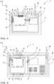
- Figure 4 illustrates schematically a second partly opened electronic component seen from above
- Figure 5 illustrates schematically a third partly opened electronic component seen from above.
- the plane defined by the x- and y-axes is parallel to the plane of a printed circuit board (PCB), later called a circuit board in this disclosure, to which the electronic component is configured to be attached.
- PCB printed circuit board
- the direction defined by the z-axis is perpendicular to the same plane of the circuit board, or a circuit board plane.
- Figure 1 shows schematically an embodiment of the electronic component, more particularly a part of an electronic component, in the direction of y-axis in cross section
- Figure 2 shows schematically an embodiment of the electronic component in the direction of y-axis in cross section
- Figures 3-5 show schematically different embodiments of the electronic component partly opened, in other words with some parts of the electronic component not in place / not shown in the figures, in the direction of the z-axis, which direction is also called "from above" in this disclosure.
- the electronic component 1 comprises a package 7 and at least one electronic chip 2, also called a chip 2 in this disclosure, housed within an enclosure inside the package 7.
- the package 7 may comprise a top, a bottom, and four sides: first side, second side, third side and a fourth side.
- the enclosure may then be formed withing the top, the bottom, and the four sides.
- Figure 2 illustrates schematically an embodiment of an electronic component 1 showing such a package in cross section
- Figures 1 and 3-5 shown embodiments of an electronic component 1 in cross section and/or with a part of the package 7 not shown to better illustrate parts of the electronic component 1 provided inside the package 7.
- the electronic chip 2 is housed within the package 7.
- the package 7 provides protection for the electronic chip(s) 2 inside the electronic component 1.
- the package 7 may be made of one material.
- the package 7 may comprise multiple materials, for instance some part(s) of the package 7 may be made of one material and some other part(s) of the package 7 from another material.
- at least a part of the package 7, such as the area of the package 7 on which the electronic chip 2 is provided and the area immediately surrounding the electronic chip 2, as shown by a rectangle around the electronic chip 2 in Figures 3-5 , may be gold-plated or formed of ceramic material.
- the package base and the cap may together form the enclosure.
- the cap may form the bottom side of the package 7.
- the cap may be made of a material different from the material of the rest of the package 7.
- the package 7 may comprise at least one of the following: a plastic material, a metal material, or a ceramic material.
- the metal material may comprise stainless steel, copper, or nickel-cobalt ferrous alloy, such as Kovar.
- the cap may comprise at least one of the following: a metal material or a ceramic material.
- the electronic component 1 may comprise a single case component.
- a single case component refers to a discrete electronic device that is enclosed within a single package or housing.
- all necessary elements and connections for the component to function are contained within the single package.
- Such single components may for instance be mounted on a circuit board or used individually depending on the application.
- the disclosed solution namely the disclosed structure of an electronic component 1 and the method for cleaning a bonding tool 8, may be particularly beneficial in connection with single case components, since they do not comprise internal structures, such as lead frame feet or suitable free space, that could be used for cleaning the bonding tool 8.
- the electronic component 1 may comprise a MEMS component.
- the electronic chip 2 may comprise at least one of the following: an accelerometer configured to measure acceleration, a gyroscope configured to measure angular rotation, or a magnetometer.
- the accelerometer or gyroscope may be a MEMS accelerometer / gyroscope.
- the electronic chip 2 comprises another type of an orientation-sensitive chip.
- the electronic component 1 further comprises at least one first bonding pad 3, at least one second bonding pad 4, and at least one bond 5 connected to at least one first bonding pad 3 and at least one second bonding pad 4 for establishing an electric connection between the electronic chip 2 and surrounding circuitry.
- the bond 5 may electrically connect the first bonding pad 3 and the second bonding pad 4.
- One of the bonding pads, for instance second bonding pad 4 may be, directly or indirectly, electrically connected to the electronic chip 2, whereby the first bonding pad 3, the second bonding pad 4, and the bond 5 may provide an electric connection between the electronic chip 2 and surrounding circuitry.
- the second bonding pad 4 being directly electrically connected to the electronic chip 2 refers to the second bonding pad 4 being attached to the electronic chip 2.
- the second bonding pad 4 being indirectly electrically connected to the electronic chip 2 refers to the second bonding pad 4 being connected to the electronic chip 2 via a further electrically conductive part or structure.
- the first bonding pad(s) 3 may be provided in the package 7 or other part(s) of the electronic component 1.
- the first bonding pad(s) 3 may be provided on an inner surface of the package 7 or other parts(s) of the electronic component 1 provided inside the package 7. More particularly, the first bonding pad(s) 3 may be provided within the enclosure. Different ways of positioning the first bonding pads 3 are shown in Figures 1 - 5 .
- at least one first bonding pad 3 may be provided in the package 7.
- at least one first bonding pad 3 may be, directly or indirectly, electrically connected to an electronic lead of the electronic component 1.
- a part of an electronic lead of the electronic component 1 may form the first bonding pad 3.
- the electronic component 1 further comprises a cleaning pad 6.
- the cleaning pad 6 is provided in the package 7.
- the cleaning pad 6 is provided inside the package 7. More particularly, the cleaning pad 6 may, thus, be enclosed within the enclosure in the electronic component 1, when the electronic component 1 is manufactured and ready to be used and/or installed.
- the cleaning pad 6 is spaced from first bonding pad(s) 3 and second bonding pad(s) 4. In other words, the cleaning pad 6 is separate from the first bonding pads 3 and second bonding pads 4. According to an embodiment, the cleaning pad 6 may be provided on an inner surface of the package 7, such as best illustrated in Figure 2 . According to an embodiment, the cleaning pad 6 may be provided on another part of the electronic component 1 provided inside the package 7.
- the cleaning pad 6 may be designed to be electrically disconnected from other structures or components. In other words, the cleaning pad 6 is not intended to be electrically connected to other parts of the electronic component 1 or surrounding circuitry, for instance to be connected to other parts of the electronic component 1 or surrounding circuitry by a bond 5.
- the bond 5 may comprise a wire bond.
- the disclosed solution namely the electronic component 1 and the method of cleaning a bonding tool 8
- the bond 5 may comprise a gold wire, a copper wire, an aluminium wire, a silver wire, a wire comprising a combination of these materials, or a wire plated with one of these materials or a with a material comprising a combination of these materials.
- the cleaning pad 6 may also be designed to enable cleaning of a bonding tool 8.
- a bonding tool 8 is a tool used for creating bonds 5 between bonding pads, for instance between first bonding pads 3 and second bonding pads 4.
- the bonding tool 8 may comprise a wire bond capillary, also called bonding capillary.
- Such a bonding tool 8 may be configured to create wire bonds between the bonding pads.
- the bonding tool 8 may comprise a bonding tool of a wire bonder machine.
- the bonding tool 8 may be configured to hold and manipulate a bonding wire during a wire bonding process.
- a tip of the bonding tool 8 may be configured to guide the bonding wire and bond it to the bonding pad(s) 3, 4.
- the cleaning pad 6 is designed to enable cleaning of the bonding tool 8 by forming at least one bond 5 on the cleaning pad 6.
- the at least one bond 5 formed for cleaning the bonding tool 8 only extends within the area of the cleaning pad 6. In other words, the at least one bond 5 formed for cleaning the bonding tool 8 does not connect the cleaning pad 6 electrically to any further parts of the electronic component 1 or surrounding circuitry.
- the cleaning pad 6 is made of a process compatible material, which is called a wire bondable material in this disclosure.
- the cleaning pad 6 is made of made of gold, nickel, silver, copper, cobalt, aluminium, tungsten, titanium, or a combination thereof.
- one or more of the first bonding pad(s) 3, the second bonding pad(s) 4, and the cleaning pad 6 are made of a same material, such as gold, nickel, silver, copper, cobalt, aluminium, tungsten, titanium, or a combination thereof.
- the surface area of the cleaning pad 6 is at least two times as large as the surface area of the smallest bonding pad 3, 4. According to an embodiment, the surface area of the cleaning pad 6 is at least two times as large as the surface area of the largest bonding pad 3, 4. In other words, the surface of the cleaning pad 6 may be clearly larger, for instance at least twice as large, as the surface of the first bonding pad(s) 3 and the second bonding pad(s) 4. Thereby, more than one bonds 5 may be provided on the cleaning pad 6.
- the package 2 may further comprise a plurality of electronic leads (not shown) protruding from the package 7 and configured to extend from at least two sides, preferably from at least two opposite sides, of the package, such as the second side and the fourth side of the package 7.
- the electronic leads may be configured to protrude from the package 7 at least in a direction corresponding to a downward direction.
- the electronic leads may further be configured to extend outwards from the package 7, for instance in a bended manner.
- the electronic leads may be used to establish electric connections from the surrounding circuitry to the electronic chip(s) 2.
- the electronic chip(s) 2 may be connected to the electronic leads inside the package 7, for example by wire bonding or flip chip bonding (not shown), and the electronic leads may extend outward from the package 7 in a side direction which is substantially perpendicular to the z-axis. Electric connections to the electronic chip(s) 2 can then be made by connecting the electronic leads to suitable connectors.
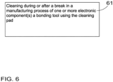
- Figure 6 illustrates schematically a method for cleaning a bonding tool.
- a method for cleaning a bonding tool may comprise cleaning 61 a bonding tool 8 during or after a break in a manufacturing process of one or more electronic component(s) 1 using the cleaning pad 6.
- the electronic component 1 may comprise an electronic component 1 according to an embodiment disclosed in this description and/or accompanying claims and drawings, or a combination of such embodiments.
- a break may comprise for instance a break caused by the structure of the electronic component 1 or a phase of the manufacturing process.
- the electronic component 1 processed may change, the position of the electronic component 1 may need to be changed, or some other intermediate phase of the process may be necessary thus causing a break in the forming of the bonds 5.
- This may cause the electronic component 1 to cool down, which may affect the quality of the first bonds 5 formed after the break.
- the bonding tool 8 may be cleaned during such a break or immediately after the break before forming first actual bond 5, which is a bond designed to establish an electric connection between the electronic chip 2 and the surrounding circuitry, to the electronic component 1.
- the cleaning of the bonding tool 8 comprises forming at least one bond 5 on the cleaning pad 6.
- the bond 5 may only extend within the area of the cleaning pad 6, as explained in connection with electronic component embodiments.
- the bond 5 may be a wire bond.
Landscapes
- Wire Bonding (AREA)
Abstract
An electronic component (1) comprises a package (7), at least one electronic chip (2) housed within an enclosure inside the package, and at least one first bonding pad (3), at least one second bonding pad (4), and at least one bond (5) connected to at least one bonding pad (3) and at least one second bonding pad (4) for establishing an electric connection between the electronic chip (2) and surrounding circuitry. A cleaning pad (6) is provided in the package (7). The cleaning pad (6) is spaced from first bonding pad(s) (3) and second bonding pad(s) (4), designed to be electrically disconnected from other structures or components, and designed to enable cleaning of a bonding tool (8).
Description
- The present disclosure relates to cleaning a bonding tool in connection with bonding of electronic components, and more particularly to an electronic component. The present disclosure further concerns a method for cleaning a bonding tool.
- Electronic chips, which may also be called dies, may be placed inside a protective package which forms an enclosure where the chip is protected from the surrounding environment. The chip may be mechanically attached to a support structure inside the enclosure, such as a die pad, and electrically connected to contacts which extend outside of the enclosure. The packaged chip thereby forms an electronic component which can be mounted on a circuit board.
- Bonding pads are widely used in connection with electronic components for establishing the electrical connections. Bonding pads are used for instance in connection with MEMS components and similar devices. Bonding pads may serve as connection points for external electrical connections allowing transfer of electrical signals, power and data between the MEMS devices and the surrounding circuitry.
- Bonding pads are typically made of conductive materials and placed to enable forming of bonds, such as wire bonds, by a bonding tool to connect the electronic component to the bonding pad and thereby to surrounding circuitry.
- A problem with bonding tools is that the manufacturing process typically does not enable continuous use of the bonding tool, but there are short breaks due to the structure of the parts or the phases of the manufacturing process during which the bonding tool is not used for implementing wire bonds. Even very short breaks, such as breaks of a couple of seconds, may cause the bonding tool to cool down. Thereby, the first wire bonds implemented after such a break may be colder. In addition, cleaning of the bonding tool may be needed for instance due to contamination of the tool due to impurities in the surrounding air or for other causes.
- An object of the present disclosure is to provide a method and an electronic component.
- The object of the disclosure is achieved by a method and an electronic component, which are characterized by what is stated in the independent claims. Some embodiments of the disclosure are disclosed in the dependent claims.
- The disclosure is based on the idea of providing the electronic component with a cleaning pad.
- An advantage of the method and electronic component of the disclosure is that the bonding tool may be cleaned on every electronic component in-situ on a cleaning site provided in the package structure. This may improve wire bonding process yield due to less downtime needed and improve quality.
- In the following the disclosure will be described in greater detail by means of preferred embodiments with reference to the accompanying drawings, in which
-
Figure 1 illustrates schematically a part of an electronic component in cross section; -
Figure 2 illustrates schematically an electronic component in cross section; -
Figure 3 illustrates schematically a partly opened electronic component seen from above; -
Figure 4 illustrates schematically a second partly opened electronic component seen from above; -
Figure 5 illustrates schematically a third partly opened electronic component seen from above; and -
Figure 6 illustrates schematically a method for cleaning a bonding tool. -
Figure 1 illustrates schematically a part of an electronic component in cross section;Figure 2 illustrates schematically an electronic component in cross section;Figure 3 illustrates schematically a partly opened electronic component seen from above;Figure 4 illustrates schematically a second partly opened electronic component seen from above; andFigure 5 illustrates schematically a third partly opened electronic component seen from above. - In the figures of this disclosure, the plane defined by the x- and y-axes is parallel to the plane of a printed circuit board (PCB), later called a circuit board in this disclosure, to which the electronic component is configured to be attached. The direction defined by the z-axis is perpendicular to the same plane of the circuit board, or a circuit board plane.
- In this disclosure, the words "bottom" and "top" only refer to how the component is configured to be placed with respect to a circuit board (PCB). The bottom side of the component is configured to be attached to the surface of the circuit board. Words such as "above" and "below" are used with the same meaning: a first part which is below a second part is configured to be closer to the circuit board, and the second part is provided on the top side of the component with respect to the first part. Words such as "bottom" and "top", "above" and "below", thus, do not refer to the orientation of the component with regard to the direction of earth's gravitational field either when the component is manufactured or when it is in use, although they can in some cases be in agreement with this conventional meaning of top / bottom when the xy-plane is horizontal.
- Referring to the axes indicated in the figures,
Figure 1 shows schematically an embodiment of the electronic component, more particularly a part of an electronic component, in the direction of y-axis in cross section,Figure 2 shows schematically an embodiment of the electronic component in the direction of y-axis in cross section, andFigures 3-5 show schematically different embodiments of the electronic component partly opened, in other words with some parts of the electronic component not in place / not shown in the figures, in the direction of the z-axis, which direction is also called "from above" in this disclosure. - The
electronic component 1 comprises apackage 7 and at least oneelectronic chip 2, also called achip 2 in this disclosure, housed within an enclosure inside thepackage 7. Thepackage 7 may comprise a top, a bottom, and four sides: first side, second side, third side and a fourth side. The enclosure may then be formed withing the top, the bottom, and the four sides.Figure 2 illustrates schematically an embodiment of anelectronic component 1 showing such a package in cross section, whereasFigures 1 and 3-5 shown embodiments of anelectronic component 1 in cross section and/or with a part of thepackage 7 not shown to better illustrate parts of theelectronic component 1 provided inside thepackage 7. - In the
electronic component 1, theelectronic chip 2 is housed within thepackage 7. Thepackage 7 provides protection for the electronic chip(s) 2 inside theelectronic component 1. According to an embodiment, thepackage 7 may be made of one material. According to another embodiment, thepackage 7 may comprise multiple materials, for instance some part(s) of thepackage 7 may be made of one material and some other part(s) of thepackage 7 from another material. According to an embodiment, at least a part of thepackage 7, such as the area of thepackage 7 on which theelectronic chip 2 is provided and the area immediately surrounding theelectronic chip 2, as shown by a rectangle around theelectronic chip 2 inFigures 3-5 , may be gold-plated or formed of ceramic material. - According to an embodiment, the
electronic component 1, more particularly thepackage 7, may comprise a package base and a cap (not shown). In such embodiments,Figures 1 - 5 may illustrate schematically a package base, or a part of the package base for instance inFigure 1 , with theelectronic chip 2 and possible other parts and devices before a cap is attached to the package base. In other embodiments, theFigures 1 - 5 may illustrate details ofelectronic components 1, where a portion of theelectronic component 1 is not shown for illustrative purposes. It should also be understood that the figures are provided for illustrative purposes, andelectronic components 1 may comprise further parts not shown in the figures. - The package base and the cap may together form the enclosure. According to an embodiment, the cap may form the bottom side of the
package 7. According to an embodiment, the cap may be made of a material different from the material of the rest of thepackage 7. According to an embodiment, thepackage 7 may comprise at least one of the following: a plastic material, a metal material, or a ceramic material. According to an embodiment, the metal material may comprise stainless steel, copper, or nickel-cobalt ferrous alloy, such as Kovar. According to an embodiment, the cap may comprise at least one of the following: a metal material or a ceramic material. - According to an embodiment, the package base may for instance be made of plastic. According to an embodiment, the package base may be manufactured in a moulding process where the package base is moulded around a leadframe, where a chip mounting element (not shown) and electronic leads have been formed. Other methods can also be used to form a plastic package base. The package base may alternatively be made of a ceramic material. The cap can be attached to the package base with glue or with any other method. The attachment region where the cap is attached to the package base may encircle the enclosure.
- According to an embodiment, the
electronic component 1 may comprise a single case component. In this disclosure, a single case component refers to a discrete electronic device that is enclosed within a single package or housing. In other words, all necessary elements and connections for the component to function are contained within the single package. Such single components may for instance be mounted on a circuit board or used individually depending on the application. The disclosed solution, namely the disclosed structure of anelectronic component 1 and the method for cleaning abonding tool 8, may be particularly beneficial in connection with single case components, since they do not comprise internal structures, such as lead frame feet or suitable free space, that could be used for cleaning thebonding tool 8. - According to an embodiment, the
electronic component 1 may comprise a MEMS component. According to an embodiment, theelectronic chip 2 may comprise at least one of the following: an accelerometer configured to measure acceleration, a gyroscope configured to measure angular rotation, or a magnetometer. The accelerometer or gyroscope may be a MEMS accelerometer / gyroscope. According to an embodiment, theelectronic chip 2 comprises another type of an orientation-sensitive chip. - The
electronic component 1 further comprises at least onefirst bonding pad 3, at least onesecond bonding pad 4, and at least onebond 5 connected to at least onefirst bonding pad 3 and at least onesecond bonding pad 4 for establishing an electric connection between theelectronic chip 2 and surrounding circuitry. In other words, thebond 5 may electrically connect thefirst bonding pad 3 and thesecond bonding pad 4. One of the bonding pads, for instancesecond bonding pad 4, may be, directly or indirectly, electrically connected to theelectronic chip 2, whereby thefirst bonding pad 3, thesecond bonding pad 4, and thebond 5 may provide an electric connection between theelectronic chip 2 and surrounding circuitry. Thesecond bonding pad 4 being directly electrically connected to theelectronic chip 2 refers to thesecond bonding pad 4 being attached to theelectronic chip 2. Thesecond bonding pad 4 being indirectly electrically connected to theelectronic chip 2 refers to thesecond bonding pad 4 being connected to theelectronic chip 2 via a further electrically conductive part or structure. - According to an embodiment, the first bonding pad(s) 3 may be provided in the
package 7 or other part(s) of theelectronic component 1. In other words, the first bonding pad(s) 3 may be provided on an inner surface of thepackage 7 or other parts(s) of theelectronic component 1 provided inside thepackage 7. More particularly, the first bonding pad(s) 3 may be provided within the enclosure. Different ways of positioning thefirst bonding pads 3 are shown inFigures 1 - 5 . According to an embodiment, at least onefirst bonding pad 3 may be provided in thepackage 7. According to an embodiment, at least onefirst bonding pad 3 may be, directly or indirectly, electrically connected to an electronic lead of theelectronic component 1. According to an embodiment, a part of an electronic lead of theelectronic component 1 may form thefirst bonding pad 3. - The
electronic component 1 further comprises acleaning pad 6. Thecleaning pad 6 is provided in thepackage 7. In other words, thecleaning pad 6 is provided inside thepackage 7. More particularly, thecleaning pad 6 may, thus, be enclosed within the enclosure in theelectronic component 1, when theelectronic component 1 is manufactured and ready to be used and/or installed. - The
cleaning pad 6 is spaced from first bonding pad(s) 3 and second bonding pad(s) 4. In other words, thecleaning pad 6 is separate from thefirst bonding pads 3 andsecond bonding pads 4. According to an embodiment, thecleaning pad 6 may be provided on an inner surface of thepackage 7, such as best illustrated inFigure 2 . According to an embodiment, thecleaning pad 6 may be provided on another part of theelectronic component 1 provided inside thepackage 7. - The
cleaning pad 6 may be designed to be electrically disconnected from other structures or components. In other words, thecleaning pad 6 is not intended to be electrically connected to other parts of theelectronic component 1 or surrounding circuitry, for instance to be connected to other parts of theelectronic component 1 or surrounding circuitry by abond 5. - According to an embodiment, the
bond 5 may comprise a wire bond. The disclosed solution, namely theelectronic component 1 and the method of cleaning abonding tool 8, may be particularly useful in connection with wire bonding and wire bonds. According to an embodiment, thebond 5 may comprise a gold wire, a copper wire, an aluminium wire, a silver wire, a wire comprising a combination of these materials, or a wire plated with one of these materials or a with a material comprising a combination of these materials. - The
cleaning pad 6 may also be designed to enable cleaning of abonding tool 8. Abonding tool 8, is a tool used for creatingbonds 5 between bonding pads, for instance betweenfirst bonding pads 3 andsecond bonding pads 4. According to an embodiment, thebonding tool 8 may comprise a wire bond capillary, also called bonding capillary. Such abonding tool 8 may be configured to create wire bonds between the bonding pads. According to an embodiment, thebonding tool 8 may comprise a bonding tool of a wire bonder machine. According to an embodiment, thebonding tool 8 may be configured to hold and manipulate a bonding wire during a wire bonding process. A tip of thebonding tool 8 may be configured to guide the bonding wire and bond it to the bonding pad(s) 3, 4. - According to an embodiment, the
cleaning pad 6 is designed to enable cleaning of thebonding tool 8 by forming at least onebond 5 on thecleaning pad 6. According to an embodiment, the at least onebond 5 formed for cleaning thebonding tool 8 only extends within the area of thecleaning pad 6. In other words, the at least onebond 5 formed for cleaning thebonding tool 8 does not connect thecleaning pad 6 electrically to any further parts of theelectronic component 1 or surrounding circuitry. - According to an embodiment, the
cleaning pad 6 is made of a process compatible material, which is called a wire bondable material in this disclosure. According to an embodiment, thecleaning pad 6 is made of made of gold, nickel, silver, copper, cobalt, aluminium, tungsten, titanium, or a combination thereof. According to an embodiment, one or more of the first bonding pad(s) 3, the second bonding pad(s) 4, and thecleaning pad 6 are made of a same material, such as gold, nickel, silver, copper, cobalt, aluminium, tungsten, titanium, or a combination thereof. - According to an embodiment, the surface area of the
cleaning pad 6 is at least two times as large as the surface area of thesmallest bonding pad cleaning pad 6 is at least two times as large as the surface area of thelargest bonding pad cleaning pad 6 may be clearly larger, for instance at least twice as large, as the surface of the first bonding pad(s) 3 and the second bonding pad(s) 4. Thereby, more than onebonds 5 may be provided on thecleaning pad 6. - According to an embodiment, as referred to, the
package 2 may further comprise a plurality of electronic leads (not shown) protruding from thepackage 7 and configured to extend from at least two sides, preferably from at least two opposite sides, of the package, such as the second side and the fourth side of thepackage 7. According to an embodiment, the electronic leads may be configured to protrude from thepackage 7 at least in a direction corresponding to a downward direction. According to an embodiment, the electronic leads may further be configured to extend outwards from thepackage 7, for instance in a bended manner. - According to an embodiment, the electronic leads may be used to establish electric connections from the surrounding circuitry to the electronic chip(s) 2. In other words, the electronic chip(s) 2 may be connected to the electronic leads inside the
package 7, for example by wire bonding or flip chip bonding (not shown), and the electronic leads may extend outward from thepackage 7 in a side direction which is substantially perpendicular to the z-axis. Electric connections to the electronic chip(s) 2 can then be made by connecting the electronic leads to suitable connectors. -
Figure 6 illustrates schematically a method for cleaning a bonding tool. - A method for cleaning a bonding tool, such as the method of
Figure 6 , may comprise cleaning 61 abonding tool 8 during or after a break in a manufacturing process of one or more electronic component(s) 1 using thecleaning pad 6. Theelectronic component 1 may comprise anelectronic component 1 according to an embodiment disclosed in this description and/or accompanying claims and drawings, or a combination of such embodiments. - In the manufacturing process of one or more
electronic components 1, a break may comprise for instance a break caused by the structure of theelectronic component 1 or a phase of the manufacturing process. For instance, theelectronic component 1 processed may change, the position of theelectronic component 1 may need to be changed, or some other intermediate phase of the process may be necessary thus causing a break in the forming of thebonds 5. This may cause theelectronic component 1 to cool down, which may affect the quality of thefirst bonds 5 formed after the break. In the method of this disclosure, and the method ofFigure 6 , thus, thebonding tool 8 may be cleaned during such a break or immediately after the break before forming firstactual bond 5, which is a bond designed to establish an electric connection between theelectronic chip 2 and the surrounding circuitry, to theelectronic component 1. - According to an embodiment, the cleaning of the
bonding tool 8 comprises forming at least onebond 5 on thecleaning pad 6. According to an embodiment, thebond 5 may only extend within the area of thecleaning pad 6, as explained in connection with electronic component embodiments. According to an embodiment, thebond 5 may be a wire bond.
Claims (12)
- An electronic component, which electronic component comprisesa package,at least one electronic chip housed within an enclosure inside the package, andat least one first bonding pad, at least one second bonding pad, and at least one bond connected to at least one bonding pad and at least one second bonding pad for establishing an electric connection between the electronic chip and surrounding circuitry, characterized in thata cleaning pad is provided in the package, which cleaning pad is spaced from first bonding pad(s) and second bonding pad(s), designed to be electrically disconnected from other structures or components, and designed to enable cleaning of a bonding tool.
- An electronic component according to claim 1, wherein the cleaning pad is made of a wire bondable material.
- An electronic component according to claim 1 or 2, wherein the cleaning pad is made of made of gold, nickel, silver, copper, cobalt, aluminium, tungsten, titanium, or a combination thereof.
- An electronic component according to claim 3, wherein the first bonding pad(s), the second bonding pad(s), and the cleaning pad are made of gold, nickel, silver, copper, cobalt, aluminium, tungsten, titanium, or a combination thereof.
- An electronic component according to any one claims 1 - 4, wherein the bond comprises a wire bond.
- An electronic component according to any one of claims 1 - 5, wherein the cleaning pad is designed to enable cleaning of the bonding tool by forming at least one bond on the cleaning pad, which bond only extends within the area of the cleaning pad.
- An electronic component according to any one of claims 1 - 6, wherein the surface area of the cleaning pad is at least two times as large as the surface area of the smallest bonding pad.
- An electronic component according to claim 7, wherein the surface area of the cleaning pad is at least two times as large as the surface area of the largest bonding pad.
- An electronic component according to any one of claims 1 - 8, wherein the electronic component comprises a single case component.
- A method for cleaning a bonding tool, characterized in that the method comprises cleaning, during or after a break in a manufacturing process of one or more electronic component(s) according to any one of claims 1 - 9, a bonding tool using the cleaning pad.
- A method according to claim 10, wherein the cleaning of the bonding tool comprises forming at least one bond on the cleaning pad, which bond only extends within the area of the cleaning pad.
- A method according to claim 11, wherein the bond is a wire bond.
Priority Applications (2)
| Application Number | Priority Date | Filing Date | Title |
|---|---|---|---|
| EP23199079.7A EP4528805A1 (en) | 2023-09-22 | 2023-09-22 | Electronic component and method for cleaning bonding tool |
| US18/887,836 US20250100025A1 (en) | 2023-09-22 | 2024-09-17 | Electronic component and method for cleaning bonding tool |
Applications Claiming Priority (1)
| Application Number | Priority Date | Filing Date | Title |
|---|---|---|---|
| EP23199079.7A EP4528805A1 (en) | 2023-09-22 | 2023-09-22 | Electronic component and method for cleaning bonding tool |
Publications (1)
| Publication Number | Publication Date |
|---|---|
| EP4528805A1 true EP4528805A1 (en) | 2025-03-26 |
Family
ID=88147055
Family Applications (1)
| Application Number | Title | Priority Date | Filing Date |
|---|---|---|---|
| EP23199079.7A Pending EP4528805A1 (en) | 2023-09-22 | 2023-09-22 | Electronic component and method for cleaning bonding tool |
Country Status (2)
| Country | Link |
|---|---|
| US (1) | US20250100025A1 (en) |
| EP (1) | EP4528805A1 (en) |
Citations (4)
| Publication number | Priority date | Publication date | Assignee | Title |
|---|---|---|---|---|
| JP2000232125A (en) * | 1999-02-12 | 2000-08-22 | Fujitsu Ten Ltd | Wire bonding equipment |
| JP2008270270A (en) * | 2007-04-16 | 2008-11-06 | Renesas Technology Corp | Manufacturing method of semiconductor device |
| JP2009004672A (en) * | 2007-06-25 | 2009-01-08 | Denso Corp | Wire bonding method |
| JP4840117B2 (en) * | 2006-12-13 | 2011-12-21 | 株式会社デンソー | Wire bonding method |
-
2023
- 2023-09-22 EP EP23199079.7A patent/EP4528805A1/en active Pending
-
2024
- 2024-09-17 US US18/887,836 patent/US20250100025A1/en active Pending
Patent Citations (4)
| Publication number | Priority date | Publication date | Assignee | Title |
|---|---|---|---|---|
| JP2000232125A (en) * | 1999-02-12 | 2000-08-22 | Fujitsu Ten Ltd | Wire bonding equipment |
| JP4840117B2 (en) * | 2006-12-13 | 2011-12-21 | 株式会社デンソー | Wire bonding method |
| JP2008270270A (en) * | 2007-04-16 | 2008-11-06 | Renesas Technology Corp | Manufacturing method of semiconductor device |
| JP2009004672A (en) * | 2007-06-25 | 2009-01-08 | Denso Corp | Wire bonding method |
Also Published As
| Publication number | Publication date |
|---|---|
| US20250100025A1 (en) | 2025-03-27 |
Similar Documents
| Publication | Publication Date | Title |
|---|---|---|
| US6891276B1 (en) | Semiconductor package device | |
| US5250841A (en) | Semiconductor device with test-only leads | |
| KR102054385B1 (en) | Resin-encapsulated semiconductor device and method of manufacturing the same | |
| US6265766B1 (en) | Flip chip adaptor package for bare die | |
| KR100651485B1 (en) | Ic die power connection using canted coil spring | |
| US8778732B2 (en) | Microelectronic devices and microelectronic support devices, and associated assemblies and methods | |
| JPH08510358A (en) | Interconnection of integrated circuit chips and substrates | |
| TW200828523A (en) | Multi-component package with both top and bottom side connection pads for three-dimensional packaging | |
| JPH0595015A (en) | Semiconductor device | |
| US7009309B1 (en) | Semiconductor package device that includes an insulative housing with a protruding peripheral portion | |
| US20040080056A1 (en) | Packaging system for die-up connection of a die-down oriented integrated circuit | |
| US20250100025A1 (en) | Electronic component and method for cleaning bonding tool | |
| US9299646B1 (en) | Lead frame with power and ground bars | |
| JPH03265148A (en) | Semiconductor device and manufacture thereof | |
| US20250273542A1 (en) | Semiconductor device | |
| JPH07249707A (en) | Semiconductor package | |
| JPH11233668A (en) | LSI package | |
| KR200159861Y1 (en) | Semiconductor package | |
| JPH05218295A (en) | Semiconductor device | |
| KR20020031881A (en) | A semiconductor package and it's manufacture method | |
| KR100259079B1 (en) | Semiconductor package and method for fabricating the same | |
| KR100386637B1 (en) | semiconductor package and method for fabricating thereof | |
| JPH06132472A (en) | IC package | |
| JP2004179300A (en) | Semiconductor device and method of manufacturing the same | |
| JPH11135554A (en) | IC package |
Legal Events
| Date | Code | Title | Description |
|---|---|---|---|
| PUAI | Public reference made under article 153(3) epc to a published international application that has entered the european phase |
Free format text: ORIGINAL CODE: 0009012 |
|
| STAA | Information on the status of an ep patent application or granted ep patent |
Free format text: STATUS: REQUEST FOR EXAMINATION WAS MADE |
|
| 17P | Request for examination filed |
Effective date: 20230922 |
|
| AK | Designated contracting states |
Kind code of ref document: A1 Designated state(s): AL AT BE BG CH CY CZ DE DK EE ES FI FR GB GR HR HU IE IS IT LI LT LU LV MC ME MK MT NL NO PL PT RO RS SE SI SK SM TR |