EP4525583A2 - Field-effect transistor, and method for manufacturing same - Google Patents
Field-effect transistor, and method for manufacturing same Download PDFInfo
- Publication number
- EP4525583A2 EP4525583A2 EP25154724.6A EP25154724A EP4525583A2 EP 4525583 A2 EP4525583 A2 EP 4525583A2 EP 25154724 A EP25154724 A EP 25154724A EP 4525583 A2 EP4525583 A2 EP 4525583A2
- Authority
- EP
- European Patent Office
- Prior art keywords
- type
- trench
- layer
- type deep
- lower layer
- Prior art date
- Legal status (The legal status is an assumption and is not a legal conclusion. Google has not performed a legal analysis and makes no representation as to the accuracy of the status listed.)
- Pending
Links
Images







Classifications
-
- H—ELECTRICITY
- H10—SEMICONDUCTOR DEVICES; ELECTRIC SOLID-STATE DEVICES NOT OTHERWISE PROVIDED FOR
- H10D—INORGANIC ELECTRIC SEMICONDUCTOR DEVICES
- H10D62/00—Semiconductor bodies, or regions thereof, of devices having potential barriers
- H10D62/10—Shapes, relative sizes or dispositions of the regions of the semiconductor bodies; Shapes of the semiconductor bodies
- H10D62/124—Shapes, relative sizes or dispositions of the regions of semiconductor bodies or of junctions between the regions
- H10D62/126—Top-view geometrical layouts of the regions or the junctions
- H10D62/127—Top-view geometrical layouts of the regions or the junctions of cellular field-effect devices, e.g. multicellular DMOS transistors or IGBTs
-
- H—ELECTRICITY
- H10—SEMICONDUCTOR DEVICES; ELECTRIC SOLID-STATE DEVICES NOT OTHERWISE PROVIDED FOR
- H10D—INORGANIC ELECTRIC SEMICONDUCTOR DEVICES
- H10D62/00—Semiconductor bodies, or regions thereof, of devices having potential barriers
- H10D62/10—Shapes, relative sizes or dispositions of the regions of the semiconductor bodies; Shapes of the semiconductor bodies
- H10D62/102—Constructional design considerations for preventing surface leakage or controlling electric field concentration
- H10D62/103—Constructional design considerations for preventing surface leakage or controlling electric field concentration for increasing or controlling the breakdown voltage of reverse-biased devices
- H10D62/105—Constructional design considerations for preventing surface leakage or controlling electric field concentration for increasing or controlling the breakdown voltage of reverse-biased devices by having particular doping profiles, shapes or arrangements of PN junctions; by having supplementary regions, e.g. junction termination extension [JTE]
-
- H—ELECTRICITY
- H10—SEMICONDUCTOR DEVICES; ELECTRIC SOLID-STATE DEVICES NOT OTHERWISE PROVIDED FOR
- H10D—INORGANIC ELECTRIC SEMICONDUCTOR DEVICES
- H10D30/00—Field-effect transistors [FET]
- H10D30/01—Manufacture or treatment
- H10D30/021—Manufacture or treatment of FETs having insulated gates [IGFET]
- H10D30/028—Manufacture or treatment of FETs having insulated gates [IGFET] of double-diffused metal oxide semiconductor [DMOS] FETs
- H10D30/0291—Manufacture or treatment of FETs having insulated gates [IGFET] of double-diffused metal oxide semiconductor [DMOS] FETs of vertical DMOS [VDMOS] FETs
- H10D30/0297—Manufacture or treatment of FETs having insulated gates [IGFET] of double-diffused metal oxide semiconductor [DMOS] FETs of vertical DMOS [VDMOS] FETs using recessing of the gate electrodes, e.g. to form trench gate electrodes
-
- H—ELECTRICITY
- H10—SEMICONDUCTOR DEVICES; ELECTRIC SOLID-STATE DEVICES NOT OTHERWISE PROVIDED FOR
- H10D—INORGANIC ELECTRIC SEMICONDUCTOR DEVICES
- H10D30/00—Field-effect transistors [FET]
- H10D30/60—Insulated-gate field-effect transistors [IGFET]
- H10D30/64—Double-diffused metal-oxide semiconductor [DMOS] FETs
- H10D30/66—Vertical DMOS [VDMOS] FETs
- H10D30/668—Vertical DMOS [VDMOS] FETs having trench gate electrodes, e.g. UMOS transistors
-
- H—ELECTRICITY
- H10—SEMICONDUCTOR DEVICES; ELECTRIC SOLID-STATE DEVICES NOT OTHERWISE PROVIDED FOR
- H10D—INORGANIC ELECTRIC SEMICONDUCTOR DEVICES
- H10D62/00—Semiconductor bodies, or regions thereof, of devices having potential barriers
- H10D62/01—Manufacture or treatment
- H10D62/051—Forming charge compensation regions, e.g. superjunctions
- H10D62/058—Forming charge compensation regions, e.g. superjunctions by using trenches, e.g. implanting into sidewalls of trenches or refilling trenches
-
- H—ELECTRICITY
- H10—SEMICONDUCTOR DEVICES; ELECTRIC SOLID-STATE DEVICES NOT OTHERWISE PROVIDED FOR
- H10D—INORGANIC ELECTRIC SEMICONDUCTOR DEVICES
- H10D62/00—Semiconductor bodies, or regions thereof, of devices having potential barriers
- H10D62/10—Shapes, relative sizes or dispositions of the regions of the semiconductor bodies; Shapes of the semiconductor bodies
- H10D62/102—Constructional design considerations for preventing surface leakage or controlling electric field concentration
- H10D62/103—Constructional design considerations for preventing surface leakage or controlling electric field concentration for increasing or controlling the breakdown voltage of reverse-biased devices
- H10D62/105—Constructional design considerations for preventing surface leakage or controlling electric field concentration for increasing or controlling the breakdown voltage of reverse-biased devices by having particular doping profiles, shapes or arrangements of PN junctions; by having supplementary regions, e.g. junction termination extension [JTE]
- H10D62/106—Constructional design considerations for preventing surface leakage or controlling electric field concentration for increasing or controlling the breakdown voltage of reverse-biased devices by having particular doping profiles, shapes or arrangements of PN junctions; by having supplementary regions, e.g. junction termination extension [JTE] having supplementary regions doped oppositely to or in rectifying contact with regions of the semiconductor bodies, e.g. guard rings with PN or Schottky junctions
- H10D62/107—Buried supplementary regions, e.g. buried guard rings
-
- H—ELECTRICITY
- H10—SEMICONDUCTOR DEVICES; ELECTRIC SOLID-STATE DEVICES NOT OTHERWISE PROVIDED FOR
- H10D—INORGANIC ELECTRIC SEMICONDUCTOR DEVICES
- H10D62/00—Semiconductor bodies, or regions thereof, of devices having potential barriers
- H10D62/10—Shapes, relative sizes or dispositions of the regions of the semiconductor bodies; Shapes of the semiconductor bodies
- H10D62/102—Constructional design considerations for preventing surface leakage or controlling electric field concentration
- H10D62/103—Constructional design considerations for preventing surface leakage or controlling electric field concentration for increasing or controlling the breakdown voltage of reverse-biased devices
- H10D62/105—Constructional design considerations for preventing surface leakage or controlling electric field concentration for increasing or controlling the breakdown voltage of reverse-biased devices by having particular doping profiles, shapes or arrangements of PN junctions; by having supplementary regions, e.g. junction termination extension [JTE]
- H10D62/109—Reduced surface field [RESURF] PN junction structures
- H10D62/111—Multiple RESURF structures, e.g. double RESURF or 3D-RESURF structures
-
- H—ELECTRICITY
- H10—SEMICONDUCTOR DEVICES; ELECTRIC SOLID-STATE DEVICES NOT OTHERWISE PROVIDED FOR
- H10D—INORGANIC ELECTRIC SEMICONDUCTOR DEVICES
- H10D62/00—Semiconductor bodies, or regions thereof, of devices having potential barriers
- H10D62/10—Shapes, relative sizes or dispositions of the regions of the semiconductor bodies; Shapes of the semiconductor bodies
- H10D62/13—Semiconductor regions connected to electrodes carrying current to be rectified, amplified or switched, e.g. source or drain regions
- H10D62/149—Source or drain regions of field-effect devices
- H10D62/151—Source or drain regions of field-effect devices of IGFETs
- H10D62/156—Drain regions of DMOS transistors
- H10D62/157—Impurity concentrations or distributions
Definitions
- the present disclosure relates to a field effect transistor, and relates to a method of manufacturing the field effect transistor.
- JP 2009-194065 A discloses a trench gate type field effect transistor.
- the field effect transistor includes multiple p-type deep layers protruding downward from a body layer. Each of the p-type deep layers extends so as to intersect trenches when a semiconductor substrate is viewed from above.
- the p-type deep layers are arranged at intervals in a width direction of the p-type deep layers. Each of the p-type deep layers extends from the body layer to a position deeper than a bottom surface of each of the trenches.
- Each of the p-type deep layers is in contact with a gate insulating film at a side surface of each of the trenches and the bottom surface of each of the trenches located below the body layer in an example of the trench gate type field effect transistor disclosed in JP 2009-194065 A .
- the field effect transistor includes an n-type drift layer in contact with the body layer and each of the p-type deep layers. When the field effect transistor is turned off, a depletion layer spreads from the body layer into the drift layer. The source-drain voltage is held by the depletion layer extending into the drift layer. When the field effect transistor is turned off, a depletion layer also spreads from each of the p-type deep layers into the drift layer.
- each of the p-type deep layers is in contact with the gate insulating film at the bottom surface of each of the trenches, the drift layer around the bottom surface of each of the trenches is depleted by the depletion layer spreading from each of the p-type deep layers.
- the depletion layer extending from each of the p-type deep layers to the periphery of the bottom surface of each of the trenches restricts the occurrence of electric field concentration in the gate insulating film and the drift layer in the vicinity of the bottom surface of each of the trenches. Therefore, the above-described field effect transistor can have a high breakdown voltage.
- the present specification proposes technology for achieving a high breakdown voltage in a field effect transistor having multiple p-type deep layers.
- a field effect transistor disclosed in the present specification includes a semiconductor substrate having a trench on an upper surface thereof, a gate insulating film covering an inner surface of the trench, and a gate electrode disposed in the trench and being insulated from the semiconductor substrate by the gate insulating film.
- the semiconductor substrate includes an n-type source layer, a p-type body layer, a p-type trench lower layer, multiple p-type deep layer, and multiple n-type deep layers.
- the source layer is in contact with the gate insulating film at a side surface of the trench.
- the body layer is in contact with the gate insulating film at the side surface of the trench located below the source layer.
- the trench lower layer is located below the trench, and extends in a longitudinal direction in a top view of the semiconductor substrate.
- Each of the p-type deep layers protrudes downward from the body layer and extends from the body layer to a position below a bottom surface of the trench.
- Each of the p-type deep layers extends in a first direction intersecting the trench in a top view of the semiconductor substrate.
- the p-type deep layers are spaced at intervals in a second direction orthogonal to the first direction in a top view of the semiconductor substrate, and is in contact with the trench lower layer located below the trench.
- Each of the multiple n-type deep layers is disposed in corresponding one of the intervals and is in contact with the gate insulating film on the side surface of the trench located below the body layer.
- the field effect transistor has the p-type trench lower layer located below the trench. Therefore, the electric field concentration around the bottom surface of the trench is relaxed when the field effect transistor is turned off. As a result, this field effect transistor can have a high breakdown voltage. Furthermore, in this field effect transistor, the p-type trench lower layer is electrically connected to the body layer through the multiple p-type deep layers. Therefore, the potential of the p-type trench lower layer is stabilized, and deterioration of the switching characteristics of the field effect transistor is suppressed. In the field effect transistor, it is possible to inhibit the deterioration of the switching characteristics while enhancing the breakdown voltage by the combination of the p-type trench lower layer and the multiple deep layers.
- a method of manufacturing a field effect transistor disclosed in the present specification includes a deep layer forming process, a trench forming process, a body layer forming process, and a p-type trench lower layer forming process.
- the deep layer forming process includes formation of multiple p-type deep layers and multiple n-type deep layers at an n-type epitaxial layer.
- Each of the multiple p-type deep layers extends in a first direction in a top view of the epitaxial layer.
- the multiple p-type deep layers are spaced at intervals in a second direction perpendicular to the first direction in the top view of the epitaxial layer.
- the multiple n-type deep layers are correspondingly located in the intervals.
- the trench forming process includes formation of a trench having a depth from a surface of the epitaxial layer to a location not exceeding a depth of each of the multiple p-type deep layers and a depth of each of the multiple n-type deep layers.
- the trench intersects the multiple p-type deep layers and the multiple n-type deep layers in the top view of the epitaxial layer.
- the body layer forming process includes formation of a body layer above the multiple p-type deep layers and the multiple n-type deep layers through ion implantation introducing of p-type impurities toward a surface of the epitaxial layer.
- the p-type trench lower layer forming process includes formation of a p-type trench lower layer below a bottom surface of the trench through the ion implantation.
- the field effect transistor According to the method of manufacturing the field effect transistor, it is possible to manufacture the field effect transistor having the p-type trench lower layer and the multiple p-type deep layers.
- FIG. 20 is a cross-sectional perspective view of a modified example of the MOSFET 10 (diagram showing the xz cross section excluding the p-type deep layers 36).
- a metal-oxide-semiconductor field effect transistor (MOSFET) 10 of an embodiment shown in FIG. 1 and FIG. 2 includes a semiconductor substrate 12.
- a direction parallel to an upper surface 12a of the semiconductor substrate 12 may also be referred to as an x-direction being perpendicular to a z-direction
- a thickness direction of the semiconductor substrate 12 may also be referred to as the z-direction
- a direction perpendicular to the x-direction and the z-direction may also be referred to as a y-direction.
- the semiconductor substrate 12 is made of silicon carbide (SiC). However, the semiconductor substrate 12 may also be made of other material such as silicon or gallium nitride.
- trenches 14 are provided from the upper surface 12a of the semiconductor substrate 12. As shown in FIG. 2 , the trenches 14 extend in the y-direction on the upper surface 12a. The trenches 14 are arranged at intervals in the x-direction.
- an inner surface (that is, a bottom surface and a side surface) of each of the trenches 14 is covered with a gate insulation film 16.
- a gate electrode 18 is disposed in each of the trenches 14. The gate electrode 18 is insulated from the semiconductor substrate 12 by the gate insulation film 16.
- an upper surface of the gate electrode 18 is covered with an interlayer insulation film 20.
- a source electrode 22 is disposed on the semiconductor substrate 12. The source electrode 22 covers each of the interlayer insulation films 20. The source electrode 22 is insulated from the gate electrodes 18 by the interlayer insulation films 20. The source electrode 22 is in contact with the upper surface 12a of the semiconductor substrate 12 at portions where the interlayer insulation films 20 are not provided.
- a drain electrode 24 is disposed at a bottom of the semiconductor substrate 12. The drain electrode 24 is in contact with the entire region of a lower surface 12b of the semiconductor substrate 12.
- the semiconductor substrate 12 includes multiple source layers 30, multiple contact layers 32, a body layer 34, multiple p-type trench lower layers 35, multiple p-type deep layers 36, multiple n-type deep layers 37, a drift layer 38, and a drain layer 40.
- Each of the source layers 30 is an n-type layer having a high n-type impurity concentration. Each of the source layers 30 is disposed in a range partially including the upper surface 12a of the semiconductor substrate 12. Each of the source layers 30 is in ohmic contact with the source electrode 22. Each of the source layers 30 is in contact with the gate insulating film 16 at an uppermost portion of the side surface of the trench 14. Each of the source layers 30 faces the gate electrode 18 with the gate insulating film 16 interposed therebetween. Each of the source layers 30 extends in the y-direction along the side surface of the trench 14. Each of the source layers 30 extends in a direction parallel to the longitudinal direction of the trench 14 when the semiconductor substrate 12 is viewed from above, and extends from an end portion of the trench 14 to another end portion of the trench 14 in the longitudinal direction.
- Each of the contact layers 32 is a p-type layer having a high p-type impurity concentration. Each of the contact layers 32 is disposed in a range partially including the upper surface 12a of the semiconductor substrate 12. Each of the contact layers 32 is disposed between two corresponding source layers 30. Each of the contact layers 32 is in ohmic contact with the source electrode 22. Each of the contact layers 32 extends in the y-direction. Each of the contact layers 32 extends in a direction parallel to the longitudinal direction of the trench 14 when the semiconductor substrate 12 is viewed from above, and extends from an end portion of the trench 14 to another end portion of the trench 14 in the longitudinal direction.
- Each of the p-type trench lower layers 35 is a p-type layer disposed below the corresponding trench 14.
- each of the p-type trench lower layers 35 may be formed in an ion implantation process, which is also adopted in the formation of the body layer 34.
- the concentration profile of p-type impurities in the depth direction of each of the p-type trench lower layers 35 and the body layer 34 is consistent.
- the depth measured from the bottom surface of the corresponding trench 14 to the lower surface of each of the p-type trench lower layers 35 matches to the depth measured from the upper surface 12a of the semiconductor substrate 12 to the lower surface of the body layer 34.
- each of the p-type trench lower layers 35 is in contact with the gate insulating film 16 covering the bottom surface of the corresponding trench 14.
- each of the p-type trench lower layers 35 may extend longer in the longitudinal direction of the corresponding trench 14 (the y-direction in this example), and may extend continuously from an end of the trench 14 to another end of the trench 14 in the longitudinal direction.
- each of the p-type trench lower layers 35 may extend longer in the longitudinal direction of the corresponding trench 14 (the y-direction in this example), and may be formed in several segments from an end of the trench 14 to another end of the trench 14 in the longitudinal direction.
- Each of the p-type deep layers 36 is a p-type layer protruding downward from the lower surface of the body layer 34.
- a p-type impurity concentration of each of the p-type deep layers 36 is higher than the p-type impurity concentration of the body layer 34 and lower than the p-type impurity concentration of the contact layer 32.
- FIG. 4 when the semiconductor substrate 12 is viewed from above, each of the p-type deep layers 36 extends in the x-direction and is orthogonal to the longitudinal direction (the y-direction in this example) of the trenches 14.
- the p-type deep layers 36 are arranged at intervals in the y-direction.
- the p-type deep layers 36 have a shape elongated in the z-direction in the yz cross section. That is, a dimension of the p-type deep layers 36 in the z-direction (hereinafter, referred to as a depth Dp) is larger than a dimension of the p-type deep layers 36 in the y-direction (hereinafter, referred to as a width Wp).
- the depth Dp can be set to 1 to 4 times the width Wp.
- each of the p-type deep layers 36 extends from the lower surface of the body layer 34 to a depth below the bottom surface of each of the trenches 14.
- Each of the p-type deep layers 36 is in contact with the gate insulating film 16 on the side surface of each of the trenches 14 located below the body layer 34.
- each of the p-type deep layers 36 is in contact with the p-type trench lower layer 35 disposed below the trench 14 to as to intersect the p-type trench lower layer 35.
- Each of the n-type deep layers 37 is an n-type layer having an n-type impurity concentration higher than that of the drift layer 38.
- the n-type impurity concentration of each of the n-type deep layers 37 is lower than the p-type impurity concentration of each of the p-type deep layers 36.
- each of the n-type deep layers 37 may have the same concentration as the n-type impurity concentration of the drift layer 38.
- each of the n-type deep layers 37 is disposed in a corresponding spacing portion 39.
- Each of the n-type deep layers 37 is in contact with the lower surface of the body layer 34.
- Each of the n-type deep layers 37 is in contact with the side surfaces of the p-type deep layer 36 on both sides thereof.
- Each of the n-type deep layers 37 extends from the lower surface of the body layer 34 to a depth below the bottom surface of each of the trenches 14 and the lower surface of each of the p-type deep layers 36.
- each of the n-type deep layers 37 in the spacing portion 39 has a shape elongated in the z-direction in the yz cross section.
- a dimension of each of the n-type deep layers 37 in the z-direction (hereinafter, referred to as a depth Dn) is larger than a dimension of each of the n-type deep layers 37 in the spacing portion 39 in the y-direction (hereinafter, referred to as a width Wn).
- the depth Dn can be set to 1 to 4 times the width Wn.
- the width Wn of each of the n-type deep layers 37 is substantially equal to the width Wp of each of the p-type deep layers 36.
- Each of the n-type deep layers 37 has a connection region 37a extending directly below the lower surface of the adjacent p-type deep layer 36.
- connection regions 37a is in contact with the lower surface of the corresponding one of the p-type deep layers 36.
- the n-type deep layers 37 are connected to each other via the connection regions 37a.
- a thickness T1 of portions where the n-type deep layers 37 protrude below the lower surfaces of the p-type deep layers 36 (that is, a distance in the z-direction from the lower surfaces of the p-type deep layers 36 to the lower surfaces of the n-type deep layers 37) is about 0.1 ⁇ m, which is extremely thin.
- each of the n-type deep layers 37 is in contact with the gate insulating film 16 on the side surface of each of the trenches 14 located below the body layer 34 in each spacing portion 39.
- each of the n-type deep layers 37 is in contact with the p-type trench lower layer 35 disposed below the trench 14 to as to intersect the p-type trench lower layer 35.
- the drift layer 38 is an n-type layer having a lower n-type impurity concentration lower than each of the n-type deep layers 37.
- the drift layer 38 is disposed below the n-type deep layers 37.
- the drift layer 38 is in contact with the n-type deep layers 37 from below.
- the drain layer 40 is an n-type layer having a higher n-type impurity concentration than the drift layer 38 and the n-type deep layers 37.
- the drain layer 40 is in contact with the drift layer 38 from below.
- the drain layer 40 is arranged in a region including a lower surface 12b of the semiconductor substrate 12.
- the drain layer 40 is in ohmic contact with the drain electrode 24.
- a higher potential is applied to the drain electrode 24 as compared to the source electrode 22.
- a potential equal to or higher than a gate threshold value is applied to each of the gate electrodes 18, a channel is formed in the body layer 34 in the vicinity of the gate insulating film 16.
- the source layers 30 and the n-type deep layers 37 are connected by the channel. Therefore, electrons flow from the source layer 30 to the drain layer 40 through the channel, the n-type deep layers 37, and the drift layer 38. That is, the MOSFET 10 is turned on.
- the potential of each of the gate electrodes 18 is reduced from a value equal to or higher than the gate threshold value to a value less than the gate threshold value, the channel disappears and the flow of electrons stops. In other words, the MOSFET 10 is turned off.
- each of the p-type trench lower layers 35 is electrically connected to the body layer 34 via each of the p-type deep layers 36, and has substantially the same potential as the body layer 34. Therefore, when the channel disappears, a reverse voltage is also applied to a pn junction at an interface between each of the p-type trench lower layers 35 and each of the n-type deep layers 37.
- each of the n-type deep layers 37 is quickly depleted by a depletion layer spreading from the body layer 34, each of the p-type trench lower layers 35 and each of the p-type deep layers 36.
- each of the p-type trench lower layers 35 is provided under the corresponding trench 14, the periphery of the bottom surface of the trench 14 is well depleted. Accordingly, the electric field concentration in the vicinities of the bottom surfaces of the trenches 14 can be greatly relaxed.
- the entire portion of each of the n-type deep layers 37 is depleted by the depletion layers extending from the body layer 34, each of the p-type trench lower layers 35, and each of the p-type deep layers 36. Note that since each of the n-type deep layers 37 has the n-type impurity concentration higher than that of the drift layer 38, a depletion layer is less likely to spread in each of the n-type deep layers 37 than in the drift layer 38.
- each of the n-type deep layers 37 is sandwiched by the p-type deep layers 36 and the width Wn of each of the n-type deep layers 37 is short, the entire portion of each of the n-type deep layers 37 is depleted.
- the depletion layer spreads to the drift layer 38 through each of the n-type deep layers 37. Since the n-type impurity concentration of the drift layer 38 is low, almost the entire portion of the drift layer 38 is depleted.
- the high voltage applied between the drain electrode 24 and the source electrode 22 is held by the depleted drift layer 38 and each of the n-type deep layers 37. Therefore, the MOSFET 10 has a high breakdown voltage.
- the p-type trench lower layer 35 is electrically connected to the body layer 34 via the p-type deep layer 36. Therefore, the potential of the p-type trench lower layer is stabilized, and deterioration of the switching characteristics of the MOSFET 10 is suppressed. In the MOSFET 10, it is possible to inhibit the deterioration of the switching characteristics while enhancing the breakdown voltage by the combination of the p-type trench lower layer 35 and the p-type deep layer 36.
- each of the n-type deep layers 37 and each of the p-type deep layers 36 have a vertically long shape.
- the feedback capacitance decreases. Accordingly, the switching speed of the MOSFET 10 can be enhanced.
- the p-type trench lower layer 35 is deeper than the p-type deep layer 36 and the n-type deep layer 37.
- the breakdown voltage of the MOSFET 10 is enhanced because the depletion of each of the n-type deep layer 37 and the drift layer 38 progresses.
- breakdown occurs in the p-type trench lower layer 35 protruding downward when an overvoltage is applied. Therefore, it is possible to reliably cause the breakdown in the cell region. As a result, the avalanche resistance of the MOSFET 10 can also be stabilized.
- the depth of the p-type trench lower layer 35 may be smaller than the depth of each of the p-type deep layer 36 and the n-type deep layer 37. In this case, since the depletion layer extending from the p-type trench lower layer 35 is suppressed, the on-resistance of the MOSFET 10 is enhanced.
- each of the p-type deep layers 36 and each of the n-type deep layers 37 continuously extend in the x-direction between adjacent trenches 14.
- each of the p-type deep layers 36 and each of the n-type deep layers 37 may be divided into several sections in the x-direction.
- each of the p-type deep layers 36 is provided in several sections, a wide current path is ensured and the on-resistance decreases.
- each of the p-type deep layers 36 and each of the n-type deep layers 37 are arranged so as to straddle the trench 14.
- each p-type deep layer 36 and each n-type deep layer 37 may be divided into several sections in the x-direction.
- a connection p-layer 36a connecting the adjacent p-type deep layers 36 in the y-direction may be provided.
- Such a connection p-layer 36a is effective in relaxing the electric field applied to the gate insulating film 16 and enhancing the breakdown voltage.
- each of the p-type trench lower layers 35 extends continuously from one end of the trench 14 to the other end of the trench 14 in the longitudinal direction.
- each of the p-type trench lower layers 35 may extend longer in the longitudinal direction of the corresponding trench 14 (the y-direction in this example), and may be formed into several segments from one end of the trench 14 to the other end of the trench 14 in the longitudinal direction.
- each of the p-type deep layers 36 passes through a portion between corresponding adjacent two of the segments of the p-type trench lower layer 35. For example, in the example shown in FIG.
- each of the source layers 30 and each of the contact layers 32 extend in parallel to the longitudinal direction of the trench 14.
- each of the source layers 30 extend in parallel to the longitudinal direction of the trench 14 and is contact with the side surface of the trench 14, it is possible to adopt the entire side surface of the trench 14 as a high-concentration channel. Therefore, the on-resistance of the MOSFET 10 is low. Furthermore, since the entire side surface of the trench 14 can be used as a channel, the channel and each of the n-type deep layers 37 are well connected.
- each of the source layers 30 extends to intersect the longitudinal direction of the trench 14, particularly perpendicular to the longitudinal direction of the trench 14, the position of the source layer 30 adjacent to the side surface of the side surface of the trench 14 is limited. Therefore, the channel with high concentration formed at the side surface of the trench 14 is also limited.
- the channel with high concentration formed on the side surface of the trench 14 and the n-type deep layer 37 are separated from each other. Since the relative positional relation is also shifted, there is a situation that the on-resistance tends to fluctuate greatly.
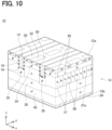
- the contact layers 32 may be distributed in the longitudinal direction of the trench 14 as shown in FIG. 10 . Also in this example, it can be said that each contact layer 32 extends in a direction parallel to the longitudinal direction of the trench 14 when the semiconductor substrate 12 is viewed from above. Also, in this example, the source layer 30 may be provided between the contact layers 32.
- the n-type deep layer 37 may have an n-type deep lower layer 137A and an n-type deep upper layer 137B.
- the n-type deep lower layer 137A is arranged below the n-type deep upper layer 137B, and is an n-type layer having higher n-type impurity concentration than the drift layer 38, and has lower n-type impurity concentration than the n-type deep upper layer 137B.
- the n-type impurity concentration of the n-type deep lower layer 137A may be the same concentration as when configured with substantially a uniform concentration as described above.
- the n-type deep upper layer 137B is arranged between the n-type deep lower layer 137A and the body layer 34, and is arranged above the bottom surface of the trench 14.
- the n-type deep upper layer 137B is in contact with the gate insulating film 16 at the side surface of the trench 14 located below the body layer 34.
- the entire n-type deep layer 37 is configured to have a high concentration equivalent to that of the n-type deep upper layer 137B, the above-described effect of enhancing the breakdown voltage is reduced.
- the n-type deep layer 37 includes the n-type deep lower layer 137A and the n-type deep upper layer 137B and the n-type deep upper layer 137B is arranged above the bottom surface of the trench 14, it is possible to suppress an increase in the on-resistance while satisfactorily enhancing the breakdown voltage.
- the p-type deep layer 36 may have a p-type deep lower layer 136A and a p-type deep upper layer 136B.
- the p-type deep lower layer 136A is provided below the p-type deep upper layer 136B, and is a p-type layer having higher p-type impurity concentration than the body layer 34 and lower p-type impurity concentration than the p-type deep upper layer 136B.
- the p-type deep upper layer 136B is arranged between the p-type deep lower layer 136A and the body layer 34, and is arranged above the bottom surface of the trench 14.
- the p-type deep upper layer 136B is in contact with the gate insulating film 16 at the side surface of the trench 14 located below the body layer 34.
- concentration of the entire p-type deep layer 36 is high.
- the thickness of the second p-type trench lower layer 135B in the depth direction may be smaller than the thickness of the source layer 30 in the thickness direction.
- the product of the p-type impurity concentration and thickness of the second p-type trench lower layer 135B may be greater than the product of the n-type impurity concentration and thickness of the n-type deep layer 37. If the second p-type trench lower layer 135B having high p-type impurity concentration is provided, the second p-type trench lower layer 135B will not be depleted when the MOSFET 10 is turned off. As a result, the capacitance, that is, the feedback capacitance between the gate electrode 18 and the drain electrode 24 decreases, and the switching speed of the MOSFET 10 can be enhanced.
- a device with a large feedback capacitance may be required.
- the relationship of p-type impurity concentration between the first p-type trench lower layer 135A and the second p-type trench lower layer 135B in FIG. 13 may be reversed. That is, the p-type impurity concentration of the second p-type trench lower layer 135B may be lower than the p-type impurity concentration of the first p-type trench lower layer 135A. Also in this case, the thickness of the second p-type trench lower layer 135B in the depth direction, in other words, z-direction may be smaller than the thickness of the source layer 30 in the thickness direction.
- the p-type trench lower layer 35 may be separated from the bottom surface of the trench 14.
- the distance between the p-type trench lower layer 35 and the bottom surface of the trench 14 may be smaller than the thickness of the source layer 30 in the thickness direction.
- the p-type trench lower layer 35 is provided in such a positional relation, the effect of enhancing the breakdown voltage can be acquired.
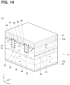
- such a p-type trench lower layer 35 has a mode that reflects the result of decreasing the number of times of ion implantation for the body layer 34 that is simultaneously formed. That is, the MOSFET 10 shown in FIG. 14 has a structure that can be manufactured at lower cost.
- the depth of the n-type deep layer 37 is deeper than the depth of the p-type deep layer 36.
- the depth of the n-type deep layer 37 may be equal to the depth of the p-type deep layer 36.
- the depth of the n-type deep layer 37 may be smaller than the depth of the p-type deep layer 36.
- each of the n-type deep layers 37 has the connection region 37a extending directly below the adjacent p-type deep layer 36.
- the n-type deep layer 37 may not have the connection region 37a.
- the p-type deep layers 36 and the n-type deep layers 37 are perpendicular to the trenches 14 when the semiconductor substrate 12 is viewed from above.
- the p-type deep layers 36 and the n-type deep layers 37 may obliquely intersect the trenches 14.
- the MOSFET 10 is manufactured from a semiconductor substrate entirely constituted by the drain layer 40.
- an epitaxial growth technique is used to form an n-type epitaxial layer 50 on the drain layer 40.
- the n-type deep layer 37 and the p-type deep layer 36 are formed by introducing the p-type impurities and the p-type impurities in a predetermined depth range apart from the surface of an epitaxial layer 50, as an example of a deep layer forming process.
- the p-type impurities are counter-doped through a mask toward a part of the range where the n-type impurities have been introduced.
- the n-type deep layer 37 and the p-type deep layer 36 may be formed by sequentially introducing the n-type impurities and the p-type impurities through masks respectively provided for the n-type deep layer 37 and the p-type deep layer 36.
- ion implantation for forming the n-type deep layer 37 can be omitted by previously adjusting the concentration of the n-type impurities to a depth corresponding to the formation range of the n-type deep layer 37 when the epitaxial layer 50 is epitaxially grown.
- the n-type deep layer 37 or the p-type deep layer 36 is formed using the ion implantation technique or the epitaxial growth technique, it is possible to form the n-type deep lower layer 137A and the n-type deep upper layer 137B as shown in FIG. 11 or form the p-type deep lower layer 136A and the p-type deep upper layer 136B by changing the concentration in the depth direction, when the n-type deep layer 37 or the p-type deep layer 36 are formed by adopting the ion implantation technique or the epitaxial growth technique.
- the source layer 30 and the contact layer 32 are formed by introducing the n-type impurities and the p-type impurities into the surface layer portion of the epitaxial layer 50 by adopting the ion implantation technique.
- an etching technique is adopted to form the trenches 14 extending from the surface of the epitaxial layer 50 to the n-type deep layer 37 and the p-type deep layer 36, as an example of the trench forming process.
- the depth of trench 14 is adjusted so as not to exceed the n-type deep layer 37 and p-type deep layer 36.
- the trench 14 intersects the multiple p-type deep layers 36 and the multiple n-type deep layers 37 when the epitaxial layer 50 is viewed from above.
- the body layer 34 and the p-type trench lower layer 35 are formed by introducing p-type impurities toward the surface of the epitaxial layer 50 in multiple stages by adopting the ion implantation technique, as an example of a body layer forming process and a p-type trench lower layer forming process.
- the body layer 34 is formed above the n-type deep layer 37 and the p-type deep layer 36 and below the source layer 30 and the contact layer 32.
- a p-type trench lower layer 35 is formed below the bottom surface of the trench 14.
- the body layer 34 and the p-type trench lower layer 35 by adopting the ion implantation technique, it is possible to form the first p-type trench lower layer 135A and the second p-type trench lower layer 135B as illustrated in FIG. 13 by modifying the concentration in the depth direction. Furthermore, the depth to which the p-type impurity is introduced to form the second p-type trench lower layer 135B is limited to a range shallower than the source layer 30. Therefore, the p-type impurity concentration of the second p-type trench lower layer 135B can be freely set while the p-type impurity concentration of the body layer 34 is set to a desired value.
- the concentration of the n-type impurities included in the source layer 30 is higher than the concentration of the introduced p-type impurities. Therefore, the electrical characteristics of the MOSFET 10 does not greatly fluctuate.
- the p-type trench lower layer 35 is formed at a position apart from the bottom surface of the trench 14.
- the MOSFET 10 shown in FIG. 14 is an example manufactured by such a method.
- a soak prevention shielding film may be formed on the side surface of the trench 14 before the ion implantation of the p-type impurities.
- the trenches 14, the gate insulating films 16, the gate electrodes 18, the interlayer insulating films 20, the source electrode 22, and the drain electrode 24 are formed. Accordingly, the MOSFET 10 is completed.
- the manufacturing method described above after the formation of the epitaxial layer 50, it is possible to form a variety of semiconductor regions by adopting the ion implantation technique without executing a re-epitaxial growth process.
- the MOSFET 10 according to the present embodiment has the p-type trench lower layer 35, the feedback capacitance is low. Therefore, in the MOSFET 10 according to the present embodiment, a low feedback capacitance can be acquired without forming the n-type deep layer 37 and the p-type deep layer 36 deeply.
- the MOSFET 10 with a low feedback capacitance can be manufactured without performing the re-epitaxial process.
- the MOSFET 10 according to the present embodiment may be manufactured by carrying out the re-epitaxial growth process, if necessary.
- the MOSFET 10 described above is an example in which the body layer 34 and the p-type trench lower layer 35 are simultaneously formed adopting the ion implantation technique after forming the trench 14.
- the p-type trench lower layer 35 and the p-type deep layer 36 may be formed simultaneously before forming the trench 14.
- the body layer 34 is formed by another ion implantation process.
- FIG. 20 shows a MOSFET 10 in which a p-type trench lower layer 35 and a p-type deep layer 36 are formed at the same time.
- the width of the p-type trench lower layer 35 is shorter than the width of the trench 14 when measured along the lateral direction of the trench 14, in other words, the x-direction.
- a field effect transistor disclosed in the present specification includes a semiconductor substrate having a trench on an upper surface thereof, a gate insulating film covering an inner surface of the trench, and a gate electrode disposed in the trench and being insulated from the semiconductor substrate by the gate insulating film.
- the material of the semiconductor substrate is not particularly limited, but may be, for example, a silicon carbide.
- the semiconductor substrate includes an n-type source layer, a p-type body layer, a p-type trench lower layer, multiple p-type deep layer, and multiple n-type deep layers.
- the source layer is in contact with the gate insulating film at a side surface of the trench.
- the body layer is in contact with the gate insulating film at the side surface of the trench located below the source layer.
- the trench lower layer is located below the trench, and extends in a longitudinal direction when the semiconductor substrate is viewed from above.
- Each of the p-type deep layers protrudes downward from the body layer, extends from the body layer to a position below a bottom surface of the trench, extends along a first direction intersecting the trench when the semiconductor substrate is viewed from above, is disposed to have a spacing portion therebetween in a second direction orthogonal to the first direction when the semiconductor substrate is viewed from above, and is in contact with the trench lower layer located below the trench.
- Each of the plurality of n-type deep layers is disposed in the corresponding spacing portion and is in contact with the gate insulating film on the side surface of the trench located below the body layer.
- the source layer may extend in a direction parallel to the longitudinal direction of the trench when the semiconductor substrate is viewed from above. In this field effect transistor, the fluctuation of the on-resistance is suppressed.
- the semiconductor substrate may have a contact layer that is provided on the body layer and has a p-type impurity concentration higher than the body layer.
- the contact layer may extend in a direction parallel to the longitudinal direction of the trench when the semiconductor substrate is viewed from above.
- the p-type trench lower layer may protrude below the p-type deep layers.
- the above-described field effect transistor can have a high breakdown voltage.
- the p-type trench lower layer may be shallower than each of the p-type deep layers. This field effect transistor can have a lower on-resistance.
- the semiconductor substrate may further include a drift layer arranged below each of the n-type deep layers and having an n-type impurity concentration lower than each of the n-type deep layers.
- each of the n-type deep layers may have a higher n-type impurity concentration than the drift layer.
- This field effect transistor can have a lower on-resistance.
- each of the n-type deep layers may have an n-type deep lower layer and an n-type deep upper layer.
- the n-type deep upper layer is disposed above the n-type deep lower layer and has an n-type impurity concentration higher than the n-type deep lower layer.
- the n-type deep upper layer is arranged above the bottom surface of the trench. This field effect transistor can achieve both high breakdown voltage and low on-resistance.
- each of the p-type deep layers may have a p-type deep lower layer and a p-type deep upper layer.
- the p-type deep upper layer is arranged above the p-type deep lower layer, and has higher p-type impurity concentration than the p-type deep lower layer.
- the p-type deep upper layer is arranged above the bottom surface of the trench. This field effect transistor can have a high breakdown voltage while suppressing an increase in leakage current.
- the depth from the bottom surface of the corresponding trench to the lower surface of each p-type trench lower layer may match the depth from the upper surface of the semiconductor substrate to the lower surface of the body layer.
- This field effect transistor has a form reflecting the result of simultaneous formation of the p-type trench lower layer and the body layer.
- This field effect transistor has a structure that can be manufactured at lower cost.
- the p-type trench lower layer may be separated from the bottom surface of the trench.
- This field effect transistor has a form reflecting the result of reducing the number of times of ion implantation of the body layer formed at the same time.
- This field effect transistor has a structure that can be manufactured at lower cost.
- the p-type trench lower layer may have multiple portions that are different in the amount of concentration in the depth direction.
- the p-type trench lower layer may have a first p-type trench lower layer and a second p-type trench lower layer arranged above the first p-type trench lower layer.
- the second p-type trench lower layer may have a higher concentration than the first p-type trench lower layer, and may have a lower concentration than the first p-type trench lower layer.
- the thickness of the second p-type trench lower layer in the depth direction may be smaller than the thickness of the source layer in the depth direction.
- the feedback capacitance can be adjusted by adjusting the impurity concentration of the p-type trench lower layer.
- the p-type trench lower layer may be formed into several segments separated from each other in the longitudinal direction of the trench. Each of the p-type deep layers may pass through a portion between corresponding adjacent two of the segments of the p-type trench lower layer. This field effect transistor suppresses an increase in leakage current.
- the multiple n-type deep layers may extend from the lower surface of the body layer to a position below the lower surface of each of the multiple p-type deep layers.
- the first direction may be orthogonal to the trench when the semiconductor substrate is viewed from above.
- a method of manufacturing a field effect transistor described in the present specification includes a deep layer forming process, a trench forming process, a body layer forming process, and a p-type trench lower layer forming process.
- the deep layer forming process includes formation of multiple p-type deep layers and multiple n-type deep layers at an n-type epitaxial layer.
- Each of the multiple p-type deep layers extends in a first direction in a top view of the epitaxial layer.
- the multiple p-type deep layers are spaced in intervals in a second direction perpendicular to the first direction in the top view of the epitaxial layer.
- the multiple n-type deep layers are correspondingly located in the intervals.
- the trench forming process includes formation of a trench having a depth from a surface of the epitaxial layer to a location not exceeding a depth of each of the multiple p-type deep layers and a depth of each of the multiple n-type deep layers.
- the trench intersects the multiple p-type deep layers and the multiple n-type deep layers in the top view of the epitaxial layer.
- the body layer forming process includes formation of a body layer above the multiple p-type deep layers and the multiple n-type deep layers through ion implantation introducing p-type impurities toward a surface of the epitaxial layer.
- the p-type trench lower layer forming process includes formation of a p-type trench lower layer below a bottom surface of the trench through the ion implantation.
- the ion implantation may be adopted to form the multiple p-type deep layers and the multiple n-type deep layers by introducing the p-type impurities and the n-type impurities in a predetermined depth range apart from the surface of the epitaxial layer. According to this manufacturing method, a field effect transistor can be manufactured without executing the re-epitaxial growth process.
- the body layer forming process and the p-type trench lower layer forming process may be performed at the same time after the trench forming process. According to the method described above, it is possible to manufacture the field effect transistor with lower cost.
- the manufacturing method may further include a source layer forming process of introducing n-type impurities into an upper layer portion of the epitaxial layer to form a source layer through the ion implantation.
- the p-type trench lower layer may have a first p-type trench lower layer and a second p-type trench lower layer arranged above the first p-type trench lower layer.
- the second p-type trench lower layer may have higher concentration than the first p-type trench lower layer, and may have lower concentration than the first p-type trench lower layer.
- the thickness of the second p-type trench lower layer in the depth direction may be smaller than the thickness of the source layer in the depth direction.
- the p-type trench lower layer forming process may be performed before the trench forming process.
- the width of the p-type trench lower layer may be smaller than the width of the trench. According to this manufacturing method, a slight misalignment between the p-type trench lower layer and the trench can be allowed.
- the p-type trench lower layer forming process may be performed along with a process of forming the multiple p-type deep layers included in the deep layer forming process at the same time. According to the method described above, it is possible to manufacture the field effect transistor with lower cost.
- a first aspect relates to a field effect transistor (10) comprising:
- a second aspect relates to a field effect transistor, further developing the field effect transistor according to the first aspect, wherein the n-type source layer extends in a direction parallel to the longitudinal direction of the trench in the top view of the semiconductor substrate.
- a third aspect relates to a field effect transistor, further developing the field effect transistor according to the first or second aspect, wherein
- a fourth aspect relates to a field effect transistor, further developing the field effect transistor according to any one of the first to third aspects, wherein
- a fifth aspect relates to a field effect transistor, further developing the field effect transistor according to any one of the first to fourth aspects, wherein
- a sixth aspect relates to a field effect transistor, further developing the field effect transistor according to any one of the first to fifth aspects, wherein a depth from the bottom surface of the trench to a lower surface of the p-type trench lower layer is identical to a depth from the upper surface of the semiconductor substrate to a lower surface of the p-type body layer.
- a seventh aspect relates to a field effect transistor, further developing the field effect transistor according to the sixth aspect, wherein the p-type trench lower layer is separated from the bottom surface of the trench.
- An eighth aspect relates to a field effect transistor, further developing the field effect transistor according to the sixth aspect, wherein
- a ninth aspect relates to a field effect transistor, further developing the field effect transistor according to the eighth aspect, wherein
- a tenth aspect relates to a field effect transistor, further developing the field effect transistor according to the eighth aspect, wherein
- An eleventh aspect relates to a field effect transistor, further developing the field effect transistor according to the ninth or tenth aspect, wherein a thickness of the second p-type trench lower layer in a depth direction of the second p-type trench lower layer is smaller than a thickness of the n-type source layer in a depth direction of the n-type source layer.
- a twelfth aspect relates to a field effect transistor, further developing the field effect transistor according to any one of the first to eleventh aspects, wherein
- a thirteenth aspect relates to a method of manufacturing a field effect transistor (10), the method comprising:
- a fourteenth aspect relates to a method, further developing the method according to the thirteenth aspect, wherein the deep layer forming process further includes forming the plurality of p-type deep layers and the plurality of n-type deep layers by introducing n-type impurities and the p-type impurities to a predetermined depth range apart from the surface of the n-type epitaxial layer through ion implantation.
- a fifteenth aspect relates to a method, further developing the method according to the thirteenth or fourteenth aspect, wherein the body layer forming process and the p-type trench lower layer forming process are executed concurrently after the trench forming process.
- a sixteenth aspect relates to a method, further developing the method according to the fifteenth aspect, further comprising:
- a seventeenth aspect relates to a method, further developing the method according to the fifteenth aspect, further comprising:
- An eighteenth aspect relates to a method, further developing the method according to the thirteenth or fourteenth aspect, wherein
- a nineteenth aspect relates to a method, further developing the method according to the eighteenth aspect, wherein the p-type trench lower layer forming process and the forming of the plurality of p-type deep layers included in the deep layer forming process are executed concurrently.
Landscapes
- Metal-Oxide And Bipolar Metal-Oxide Semiconductor Integrated Circuits (AREA)
- Insulated Gate Type Field-Effect Transistor (AREA)
- Electrodes Of Semiconductors (AREA)
Abstract
Description
- The present application is based on
Japanese Patent Application No. 2021-0039221 filed on March 11, 2021 Japanese Patent Application No. 2021-069123 filed on April 15, 2021 Japanese Patent Application No. 2021-103917 filed on June 23, 2021 - The present disclosure relates to a field effect transistor, and relates to a method of manufacturing the field effect transistor.
-
JP 2009-194065 A JP 2009-194065 A - It is required to provide technology for further relieving electric field concentration at a gate insulating film around the bottom surface of a trench and enhancing a breakdown voltage in a field effect transistor having multiple p-type deep layers. The present specification proposes technology for achieving a high breakdown voltage in a field effect transistor having multiple p-type deep layers.
- A field effect transistor disclosed in the present specification includes a semiconductor substrate having a trench on an upper surface thereof, a gate insulating film covering an inner surface of the trench, and a gate electrode disposed in the trench and being insulated from the semiconductor substrate by the gate insulating film. The semiconductor substrate includes an n-type source layer, a p-type body layer, a p-type trench lower layer, multiple p-type deep layer, and multiple n-type deep layers. The source layer is in contact with the gate insulating film at a side surface of the trench. The body layer is in contact with the gate insulating film at the side surface of the trench located below the source layer. The trench lower layer is located below the trench, and extends in a longitudinal direction in a top view of the semiconductor substrate. Each of the p-type deep layers protrudes downward from the body layer and extends from the body layer to a position below a bottom surface of the trench. Each of the p-type deep layers extends in a first direction intersecting the trench in a top view of the semiconductor substrate. The p-type deep layers are spaced at intervals in a second direction orthogonal to the first direction in a top view of the semiconductor substrate, and is in contact with the trench lower layer located below the trench. Each of the multiple n-type deep layers is disposed in corresponding one of the intervals and is in contact with the gate insulating film on the side surface of the trench located below the body layer.
- The field effect transistor has the p-type trench lower layer located below the trench. Therefore, the electric field concentration around the bottom surface of the trench is relaxed when the field effect transistor is turned off. As a result, this field effect transistor can have a high breakdown voltage. Furthermore, in this field effect transistor, the p-type trench lower layer is electrically connected to the body layer through the multiple p-type deep layers. Therefore, the potential of the p-type trench lower layer is stabilized, and deterioration of the switching characteristics of the field effect transistor is suppressed. In the field effect transistor, it is possible to inhibit the deterioration of the switching characteristics while enhancing the breakdown voltage by the combination of the p-type trench lower layer and the multiple deep layers.
- A method of manufacturing a field effect transistor disclosed in the present specification includes a deep layer forming process, a trench forming process, a body layer forming process, and a p-type trench lower layer forming process. The deep layer forming process includes formation of multiple p-type deep layers and multiple n-type deep layers at an n-type epitaxial layer. Each of the multiple p-type deep layers extends in a first direction in a top view of the epitaxial layer. The multiple p-type deep layers are spaced at intervals in a second direction perpendicular to the first direction in the top view of the epitaxial layer. The multiple n-type deep layers are correspondingly located in the intervals. The trench forming process includes formation of a trench having a depth from a surface of the epitaxial layer to a location not exceeding a depth of each of the multiple p-type deep layers and a depth of each of the multiple n-type deep layers. The trench intersects the multiple p-type deep layers and the multiple n-type deep layers in the top view of the epitaxial layer. The body layer forming process includes formation of a body layer above the multiple p-type deep layers and the multiple n-type deep layers through ion implantation introducing of p-type impurities toward a surface of the epitaxial layer. The p-type trench lower layer forming process includes formation of a p-type trench lower layer below a bottom surface of the trench through the ion implantation.
- According to the method of manufacturing the field effect transistor, it is possible to manufacture the field effect transistor having the p-type trench lower layer and the multiple p-type deep layers.
-
-
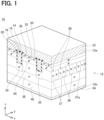
FIG. 1 is a cross-sectional perspective view of the MOSFET 10 (diagram showing an xz cross section excluding the p-type deep layers 36). -
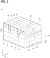
FIG. 2 is a cross-sectional perspective view of theMOSFET 10 omitting thesource electrode 22 and the interlayer insulating film 20 (diagram showing the xz cross section excluding the p-type deep layers 36). -
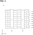
FIG. 3 is an enlarged xy cross-sectional view including a p-type trenchlower layer 35, the p-typedeep layers 36 and n-typedeep layers 37, and is an enlarged cross-sectional view of theMOSFET 10 illustrating the arrangement of the p-type trenchlower layer 35, the p-typedeep layers 36 and the n-typedeep layers 37 in a top view of thesemiconductor substrate 12. -
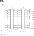
FIG. 4 is an enlarged xy cross-sectional view including atrench 14, the p-typedeep layers 36 and n-typedeep layers 37, and is an enlarged cross-sectional view of theMOSFET 10 illustrating the arrangement of thetrench 14, the p-typedeep layers 36 and the n-typedeep layers 37 in a top view of thesemiconductor substrate 12. -
FIG. 5 is an enlarged yz cross-sectional view of theMOSFET 10 including the p-typedeep layers 36 and the n-typedeep layers 37. -
FIG. 6 is a cross-sectional perspective view of the MOSFET 10 (diagram showing an xz cross section including the p-type deep layers 36). -
FIG. 7 is an enlarged xy cross-sectional view including thetrench 14, the p-typedeep layers 36 and the n-typedeep layers 37, and is an enlarged cross-sectional view of a modified example of theMOSFET 10 illustrating the arrangement of thetrench 14, the p-typedeep layers 36 and the n-typedeep layers 37 in the top view of thesemiconductor substrate 12. -
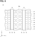
FIG. 8 is an enlarged xy cross-sectional view including thetrench 14, the p-typedeep layers 36 and the n-typedeep layers 37, and is an enlarged cross-sectional view of a modified example of theMOSFET 10 illustrating the arrangement of thetrench 14, the p-typedeep layers 36 and the n-typedeep layers 37 in the top view of thesemiconductor substrate 12. -
FIG. 9 is an enlarged xy cross-sectional view including the p-type trenchlower layer 35, the p-typedeep layers 36 and n-typedeep layers 37, and is an enlarged cross-sectional view of a modified example of theMOSFET 10 illustrating the arrangement of the p-type trenchlower layer 35, the p-typedeep layers 36 and the n-typedeep layers 37 in the top view of thesemiconductor substrate 12. -
FIG. 10 is a cross-sectional perspective view of a modified example of theMOSFET 10 omitting thesource electrode 22 and the interlayer insulating film 20 (diagram showing the xz cross section excluding the p-type deep layers 36). -
FIG. 11 is a cross-sectional perspective view of a modified example of the MOSFET 10 (diagram showing the xz cross section excluding the p-type deep layers 36). -
FIG. 12 is a cross-sectional perspective view of a modified example of the MOSFET 10 (diagram showing an xz cross section including the p-type deep layers 36). -
FIG. 13 is a cross-sectional perspective view of a modified example of the MOSFET 10 (diagram showing the xz cross section excluding the p-type deep layers 36). -
FIG. 14 is a cross-sectional perspective view of a modified example of the MOSFET 10 (diagram showing the xz cross section including the p-type deep layers 36). -
FIG. 15 is an explanatory diagram of a manufacturing method of theMOSFET 10. -
FIG. 16 is an explanatory diagram of a manufacturing method of theMOSFET 10. -
FIG. 17 is an explanatory diagram of a manufacturing method of theMOSFET 10. -
FIG. 18 is an explanatory diagram of a manufacturing method of theMOSFET 10. -
FIG. 19 is an explanatory diagram of a manufacturing method of theMOSFET 10. -
FIG. 20 is a cross-sectional perspective view of a modified example of the MOSFET 10 (diagram showing the xz cross section excluding the p-type deep layers 36). - A metal-oxide-semiconductor field effect transistor (MOSFET) 10 of an embodiment shown in
FIG. 1 andFIG. 2 includes asemiconductor substrate 12. In the following, a direction parallel to anupper surface 12a of thesemiconductor substrate 12 may also be referred to as an x-direction being perpendicular to a z-direction, a thickness direction of thesemiconductor substrate 12 may also be referred to as the z-direction, and a direction perpendicular to the x-direction and the z-direction may also be referred to as a y-direction. Thesemiconductor substrate 12 is made of silicon carbide (SiC). However, thesemiconductor substrate 12 may also be made of other material such as silicon or gallium nitride.Multiple trenches 14 are provided from theupper surface 12a of thesemiconductor substrate 12. As shown inFIG. 2 , thetrenches 14 extend in the y-direction on theupper surface 12a. Thetrenches 14 are arranged at intervals in the x-direction. - As shown in
FIG. 1 andFIG. 2 , an inner surface (that is, a bottom surface and a side surface) of each of thetrenches 14 is covered with agate insulation film 16. Agate electrode 18 is disposed in each of thetrenches 14. Thegate electrode 18 is insulated from thesemiconductor substrate 12 by thegate insulation film 16. As shown inFIG. 1 , an upper surface of thegate electrode 18 is covered with aninterlayer insulation film 20. Asource electrode 22 is disposed on thesemiconductor substrate 12. The source electrode 22 covers each of theinterlayer insulation films 20. Thesource electrode 22 is insulated from thegate electrodes 18 by theinterlayer insulation films 20. Thesource electrode 22 is in contact with theupper surface 12a of thesemiconductor substrate 12 at portions where theinterlayer insulation films 20 are not provided. Adrain electrode 24 is disposed at a bottom of thesemiconductor substrate 12. Thedrain electrode 24 is in contact with the entire region of alower surface 12b of thesemiconductor substrate 12. - As shown in
FIG. 1 andFIG. 2 , thesemiconductor substrate 12 includes multiple source layers 30, multiple contact layers 32, abody layer 34, multiple p-type trenchlower layers 35, multiple p-typedeep layers 36, multiple n-typedeep layers 37, adrift layer 38, and adrain layer 40. - Each of the source layers 30 is an n-type layer having a high n-type impurity concentration. Each of the source layers 30 is disposed in a range partially including the
upper surface 12a of thesemiconductor substrate 12. Each of the source layers 30 is in ohmic contact with thesource electrode 22. Each of the source layers 30 is in contact with thegate insulating film 16 at an uppermost portion of the side surface of thetrench 14. Each of the source layers 30 faces thegate electrode 18 with thegate insulating film 16 interposed therebetween. Each of the source layers 30 extends in the y-direction along the side surface of thetrench 14. Each of the source layers 30 extends in a direction parallel to the longitudinal direction of thetrench 14 when thesemiconductor substrate 12 is viewed from above, and extends from an end portion of thetrench 14 to another end portion of thetrench 14 in the longitudinal direction. - Each of the contact layers 32 is a p-type layer having a high p-type impurity concentration. Each of the contact layers 32 is disposed in a range partially including the
upper surface 12a of thesemiconductor substrate 12. Each of the contact layers 32 is disposed between two corresponding source layers 30. Each of the contact layers 32 is in ohmic contact with thesource electrode 22. Each of the contact layers 32 extends in the y-direction. Each of the contact layers 32 extends in a direction parallel to the longitudinal direction of thetrench 14 when thesemiconductor substrate 12 is viewed from above, and extends from an end portion of thetrench 14 to another end portion of thetrench 14 in the longitudinal direction. - The
body layer 34 is a p-type layer having a lower p-type impurity concentration than the contact layers 32. Thebody layer 34 is disposed below the source layers 30 and the contact layers 32. Thebody layer 34 is in contact with the source layers 30 and the contact layers 32 from below. Thebody layer 34 is in contact with thegate insulating film 16 on the side surface of thetrench 14 located below thesource layer 30. Thebody layer 34 faces thegate electrode 18 with thegate insulating film 16 interposed therebetween. - Each of the p-type trench
lower layers 35 is a p-type layer disposed below the correspondingtrench 14. As will be described later, each of the p-type trenchlower layers 35 may be formed in an ion implantation process, which is also adopted in the formation of thebody layer 34. In this case, the concentration profile of p-type impurities in the depth direction of each of the p-type trenchlower layers 35 and thebody layer 34 is consistent. The depth measured from the bottom surface of the correspondingtrench 14 to the lower surface of each of the p-type trenchlower layers 35 matches to the depth measured from theupper surface 12a of thesemiconductor substrate 12 to the lower surface of thebody layer 34. In this example, each of the p-type trenchlower layers 35 is in contact with thegate insulating film 16 covering the bottom surface of the correspondingtrench 14. As shown inFIG. 3 , when thesemiconductor substrate 12 is viewed from above, each of the p-type trenchlower layers 35 may extend longer in the longitudinal direction of the corresponding trench 14 (the y-direction in this example), and may extend continuously from an end of thetrench 14 to another end of thetrench 14 in the longitudinal direction. As described hereinafter, each of the p-type trenchlower layers 35 may extend longer in the longitudinal direction of the corresponding trench 14 (the y-direction in this example), and may be formed in several segments from an end of thetrench 14 to another end of thetrench 14 in the longitudinal direction. - Each of the p-type
deep layers 36 is a p-type layer protruding downward from the lower surface of thebody layer 34. A p-type impurity concentration of each of the p-typedeep layers 36 is higher than the p-type impurity concentration of thebody layer 34 and lower than the p-type impurity concentration of thecontact layer 32. As shown inFIG. 4 , when thesemiconductor substrate 12 is viewed from above, each of the p-typedeep layers 36 extends in the x-direction and is orthogonal to the longitudinal direction (the y-direction in this example) of thetrenches 14. The p-typedeep layers 36 are arranged at intervals in the y-direction. Hereinafter, a portion between the p-typedeep layers 36 is referred to as a spacing portion 39 (seeFIGS. 1 and2 ). As shown inFIG. 5 , the p-typedeep layers 36 have a shape elongated in the z-direction in the yz cross section. That is, a dimension of the p-typedeep layers 36 in the z-direction (hereinafter, referred to as a depth Dp) is larger than a dimension of the p-typedeep layers 36 in the y-direction (hereinafter, referred to as a width Wp). For example, the depth Dp can be set to 1 to 4 times the width Wp. As shown inFIG.6 , each of the p-typedeep layers 36 extends from the lower surface of thebody layer 34 to a depth below the bottom surface of each of thetrenches 14. Each of the p-typedeep layers 36 is in contact with thegate insulating film 16 on the side surface of each of thetrenches 14 located below thebody layer 34. As shown inFIG. 3 , each of the p-typedeep layers 36 is in contact with the p-type trenchlower layer 35 disposed below thetrench 14 to as to intersect the p-type trenchlower layer 35. - Each of the n-type
deep layers 37 is an n-type layer having an n-type impurity concentration higher than that of thedrift layer 38. The n-type impurity concentration of each of the n-typedeep layers 37 is lower than the p-type impurity concentration of each of the p-type deep layers 36. Instead of this example, each of the n-typedeep layers 37 may have the same concentration as the n-type impurity concentration of thedrift layer 38. As shown inFIG. 1 andFIG. 2 , each of the n-typedeep layers 37 is disposed in acorresponding spacing portion 39. Each of the n-typedeep layers 37 is in contact with the lower surface of thebody layer 34. Each of the n-typedeep layers 37 is in contact with the side surfaces of the p-typedeep layer 36 on both sides thereof. Each of the n-typedeep layers 37 extends from the lower surface of thebody layer 34 to a depth below the bottom surface of each of thetrenches 14 and the lower surface of each of the p-type deep layers 36. As shown inFIG. 5 , each of the n-typedeep layers 37 in thespacing portion 39 has a shape elongated in the z-direction in the yz cross section. That is, a dimension of each of the n-typedeep layers 37 in the z-direction (hereinafter, referred to as a depth Dn) is larger than a dimension of each of the n-typedeep layers 37 in thespacing portion 39 in the y-direction (hereinafter, referred to as a width Wn). For example, the depth Dn can be set to 1 to 4 times the width Wn. In the present embodiment, the width Wn of each of the n-typedeep layers 37 is substantially equal to the width Wp of each of the p-type deep layers 36. Each of the n-typedeep layers 37 has aconnection region 37a extending directly below the lower surface of the adjacent p-typedeep layer 36. Each of theconnection regions 37a is in contact with the lower surface of the corresponding one of the p-type deep layers 36. The n-typedeep layers 37 are connected to each other via theconnection regions 37a. A thickness T1 of portions where the n-typedeep layers 37 protrude below the lower surfaces of the p-type deep layers 36 (that is, a distance in the z-direction from the lower surfaces of the p-typedeep layers 36 to the lower surfaces of the n-type deep layers 37) is about 0.1 µm, which is extremely thin. As illustrated inFIGS. 1 and2 , each of the n-typedeep layers 37 is in contact with thegate insulating film 16 on the side surface of each of thetrenches 14 located below thebody layer 34 in each spacingportion 39. As shown inFIG. 3 , each of the n-typedeep layers 37 is in contact with the p-type trenchlower layer 35 disposed below thetrench 14 to as to intersect the p-type trenchlower layer 35. - The
drift layer 38 is an n-type layer having a lower n-type impurity concentration lower than each of the n-type deep layers 37. Thedrift layer 38 is disposed below the n-type deep layers 37. Thedrift layer 38 is in contact with the n-typedeep layers 37 from below. - The
drain layer 40 is an n-type layer having a higher n-type impurity concentration than thedrift layer 38 and the n-type deep layers 37. Thedrain layer 40 is in contact with thedrift layer 38 from below. Thedrain layer 40 is arranged in a region including alower surface 12b of thesemiconductor substrate 12. Thedrain layer 40 is in ohmic contact with thedrain electrode 24. - The following describes an operation of the
MOSFET 10. When theMOSFET 10 is used, a higher potential is applied to thedrain electrode 24 as compared to thesource electrode 22. When a potential equal to or higher than a gate threshold value is applied to each of thegate electrodes 18, a channel is formed in thebody layer 34 in the vicinity of thegate insulating film 16. The source layers 30 and the n-typedeep layers 37 are connected by the channel. Therefore, electrons flow from thesource layer 30 to thedrain layer 40 through the channel, the n-typedeep layers 37, and thedrift layer 38. That is, theMOSFET 10 is turned on. When the potential of each of thegate electrodes 18 is reduced from a value equal to or higher than the gate threshold value to a value less than the gate threshold value, the channel disappears and the flow of electrons stops. In other words, theMOSFET 10 is turned off. - Next, the operation when the
MOSFET 10 is turned off will be described in more detail. When the channel disappears, a reverse voltage is applied to a pn junction at an interface between thebody layer 34 and each of the n-type deep layers 37. Therefore, a depletion layer spreads from thebody layer 34 to each of the n-type deep layers 37. Each of the p-typedeep layers 36 is electrically connected to thebody layer 34 and has substantially the same potential as thebody layer 34. Therefore, when the channel disappears, a reverse voltage is also applied to a pn junction at an interface between each of the p-typedeep layers 36 and each of the n-type deep layers 37. Therefore, a depletion layer also spreads from each of the p-typedeep layers 36 to each of the n-type deep layers 37. Furthermore, each of the p-type trenchlower layers 35 is electrically connected to thebody layer 34 via each of the p-typedeep layers 36, and has substantially the same potential as thebody layer 34. Therefore, when the channel disappears, a reverse voltage is also applied to a pn junction at an interface between each of the p-type trenchlower layers 35 and each of the n-type deep layers 37. Thus, each of the n-typedeep layers 37 is quickly depleted by a depletion layer spreading from thebody layer 34, each of the p-type trenchlower layers 35 and each of the p-type deep layers 36. In particular, since each of the p-type trenchlower layers 35 is provided under the correspondingtrench 14, the periphery of the bottom surface of thetrench 14 is well depleted. Accordingly, the electric field concentration in the vicinities of the bottom surfaces of thetrenches 14 can be greatly relaxed. In addition, the entire portion of each of the n-typedeep layers 37 is depleted by the depletion layers extending from thebody layer 34, each of the p-type trenchlower layers 35, and each of the p-type deep layers 36. Note that since each of the n-typedeep layers 37 has the n-type impurity concentration higher than that of thedrift layer 38, a depletion layer is less likely to spread in each of the n-typedeep layers 37 than in thedrift layer 38. Since each of the n-typedeep layers 37 is sandwiched by the p-typedeep layers 36 and the width Wn of each of the n-typedeep layers 37 is short, the entire portion of each of the n-typedeep layers 37 is depleted. The depletion layer spreads to thedrift layer 38 through each of the n-type deep layers 37. Since the n-type impurity concentration of thedrift layer 38 is low, almost the entire portion of thedrift layer 38 is depleted. The high voltage applied between thedrain electrode 24 and thesource electrode 22 is held by the depleteddrift layer 38 and each of the n-type deep layers 37. Therefore, theMOSFET 10 has a high breakdown voltage. - Also, in the
MOSFET 10, the p-type trenchlower layer 35 is electrically connected to thebody layer 34 via the p-typedeep layer 36. Therefore, the potential of the p-type trench lower layer is stabilized, and deterioration of the switching characteristics of theMOSFET 10 is suppressed. In theMOSFET 10, it is possible to inhibit the deterioration of the switching characteristics while enhancing the breakdown voltage by the combination of the p-type trenchlower layer 35 and the p-typedeep layer 36. - In the
MOSFET 10, the p-type trenchlower layer 35 is in contact with thegate insulating film 16 covering the bottom surface of thetrench 14. As a result, the capacitance (that is, feedback capacitance) between thegate electrode 18 and thedrain electrode 24 decreases. In addition, in theMOSFET 10 of the present embodiment, each of the n-typedeep layers 37 and each of the p-typedeep layers 36 have a vertically long shape. When each of the n-typedeep layers 37 and each of the p-typedeep layers 36 are configured as described above, the feedback capacitance decreases. Accordingly, the switching speed of theMOSFET 10 can be enhanced. - Also, in the
MOSFET 10, the p-type trenchlower layer 35 is deeper than the p-typedeep layer 36 and the n-typedeep layer 37. When such a deep p-type trenchlower layer 35 is provided, the breakdown voltage of theMOSFET 10 is enhanced because the depletion of each of the n-typedeep layer 37 and thedrift layer 38 progresses. Further, when such a deep p-type trenchlower layer 35 is provided, breakdown occurs in the p-type trenchlower layer 35 protruding downward when an overvoltage is applied. Therefore, it is possible to reliably cause the breakdown in the cell region. As a result, the avalanche resistance of theMOSFET 10 can also be stabilized. The depth of the p-type trenchlower layer 35 may be smaller than the depth of each of the p-typedeep layer 36 and the n-typedeep layer 37. In this case, since the depletion layer extending from the p-type trenchlower layer 35 is suppressed, the on-resistance of theMOSFET 10 is enhanced. - As shown in
FIG. 4 , in theMOSFET 10, when thesemiconductor substrate 12 is viewed from above, each of the p-typedeep layers 36 and each of the n-typedeep layers 37 continuously extend in the x-direction betweenadjacent trenches 14. Instead of this example, as shown inFIG. 7 , each of the p-typedeep layers 36 and each of the n-typedeep layers 37 may be divided into several sections in the x-direction. In this example, since each of the p-typedeep layers 36 is provided in several sections, a wide current path is ensured and the on-resistance decreases. However, even in this example, each of the p-typedeep layers 36 and each of the n-typedeep layers 37 are arranged so as to straddle thetrench 14. Thereby, the above-described effects can be exhibited. It is noted that only one of each p-typedeep layer 36 and each n-typedeep layer 37 may be divided into several sections in the x-direction. Further, as shown inFIG. 8 , a connection p-layer 36a connecting the adjacent p-typedeep layers 36 in the y-direction may be provided. Such a connection p-layer 36a is effective in relaxing the electric field applied to thegate insulating film 16 and enhancing the breakdown voltage. - In the
MOSFET 10, as shown inFIG. 3 , when thesemiconductor substrate 12 is viewed from above, each of the p-type trenchlower layers 35 extends continuously from one end of thetrench 14 to the other end of thetrench 14 in the longitudinal direction. As shown inFIG. 9 , when thesemiconductor substrate 12 is viewed from above, each of the p-type trenchlower layers 35 may extend longer in the longitudinal direction of the corresponding trench 14 (the y-direction in this example), and may be formed into several segments from one end of thetrench 14 to the other end of thetrench 14 in the longitudinal direction. In this case, each of the p-typedeep layers 36 passes through a portion between corresponding adjacent two of the segments of the p-type trenchlower layer 35. For example, in the example shown inFIG. 3 , there is a concern about an increase in a damage at the portion where the p-type trenchlower layer 35 and the p-typedeep layer 36 overlap during ion implantation, and there is a concern about an increase in leakage current. On the other hand, in the example shown inFIG. 9 , since the overlapping portion between the p-type trenchlower layer 35 and the p-typedeep layer 36 is small, an increase in leakage current can be suppressed. - As shown in
FIG. 2 , in theMOSFET 10, when thesemiconductor substrate 12 is viewed from above, each of the source layers 30 and each of the contact layers 32 extend in parallel to the longitudinal direction of thetrench 14. In particular, each of the source layers 30 extend in parallel to the longitudinal direction of thetrench 14 and is contact with the side surface of thetrench 14, it is possible to adopt the entire side surface of thetrench 14 as a high-concentration channel. Therefore, the on-resistance of theMOSFET 10 is low. Furthermore, since the entire side surface of thetrench 14 can be used as a channel, the channel and each of the n-typedeep layers 37 are well connected. For example, if each of the source layers 30 extends to intersect the longitudinal direction of thetrench 14, particularly perpendicular to the longitudinal direction of thetrench 14, the position of thesource layer 30 adjacent to the side surface of the side surface of thetrench 14 is limited. Therefore, the channel with high concentration formed at the side surface of thetrench 14 is also limited. In such an example, due to misalignment in a positional relation between thesource layer 30 and the n-typedeep layer 37 during manufacturing, the channel with high concentration formed on the side surface of thetrench 14 and the n-typedeep layer 37 are separated from each other. Since the relative positional relation is also shifted, there is a situation that the on-resistance tends to fluctuate greatly. On the other hand, in theMOSFET 10, since the entire side surface of thetrench 14 can be used as a high-concentration channel, such fluctuation in on-resistance does not occur. Instead of the example shown inFIG. 2 , the contact layers 32 may be distributed in the longitudinal direction of thetrench 14 as shown inFIG. 10 . Also in this example, it can be said that eachcontact layer 32 extends in a direction parallel to the longitudinal direction of thetrench 14 when thesemiconductor substrate 12 is viewed from above. Also, in this example, thesource layer 30 may be provided between the contact layers 32. - Further, in the
MOSFET 10, as shown inFIG. 11 , the n-typedeep layer 37 may have an n-type deeplower layer 137A and an n-type deepupper layer 137B. The n-type deeplower layer 137A is arranged below the n-type deepupper layer 137B, and is an n-type layer having higher n-type impurity concentration than thedrift layer 38, and has lower n-type impurity concentration than the n-type deepupper layer 137B. The n-type impurity concentration of the n-type deeplower layer 137A may be the same concentration as when configured with substantially a uniform concentration as described above. The n-type deepupper layer 137B is arranged between the n-type deeplower layer 137A and thebody layer 34, and is arranged above the bottom surface of thetrench 14. The n-type deepupper layer 137B is in contact with thegate insulating film 16 at the side surface of thetrench 14 located below thebody layer 34. When such an n-type deepupper layer 137B is provided, the depletion layer extending from both of the p-type trenchlower layer 35 and thebody layer 34 narrows the current path in the region between the p-type trenchlower layer 35 and thebody layer 34. A phenomenon (JFET effect) can be suppressed, and an increase in on-resistance can be suppressed. If the entire n-typedeep layer 37 is configured to have a high concentration equivalent to that of the n-type deepupper layer 137B, the above-described effect of enhancing the breakdown voltage is reduced. When the n-typedeep layer 37 includes the n-type deeplower layer 137A and the n-type deepupper layer 137B and the n-type deepupper layer 137B is arranged above the bottom surface of thetrench 14, it is possible to suppress an increase in the on-resistance while satisfactorily enhancing the breakdown voltage. - In the
MOSFET 10, as shown inFIG. 12 , the p-typedeep layer 36 may have a p-type deeplower layer 136A and a p-type deepupper layer 136B. The p-type deeplower layer 136A is provided below the p-type deepupper layer 136B, and is a p-type layer having higher p-type impurity concentration than thebody layer 34 and lower p-type impurity concentration than the p-type deepupper layer 136B. The p-type deepupper layer 136B is arranged between the p-type deeplower layer 136A and thebody layer 34, and is arranged above the bottom surface of thetrench 14. The p-type deepupper layer 136B is in contact with thegate insulating film 16 at the side surface of thetrench 14 located below thebody layer 34. In order to enhance the breakdown voltage of theMOSFET 10, it may be desirable that the concentration of the entire p-typedeep layer 36 is high. However, there may be a concern about an increase in a leakage current as the damage during the ion implantation at the portion where the p-typedeep layer 36 overlaps the p-type trenchlower layer 35 increases. In theMOSFET 10 as shown inFIG. 12 , by increasing the concentration of the p-type deepupper layer 136B at a portion where the p-type deepupper layer 136B does not overlap the p-type trenchlower layer 35, it is possible to suppress an increase in the leakage current while enhancing the breakdown voltage. - In the
MOSFET 10, as shown inFIG. 13 , the p-type trenchlower layer 35 may have a first p-type trenchlower layer 135A and a second p-type trenchlower layer 135B. The first p-type trenchlower layer 135A is provided below the second p-type trenchlower layer 135B, and is a p-type layer with lower p-type impurity concentration than the second p-type trenchlower layer 135B. The second p-typelower layer 135B is provided between the first p-type trenchlower layer 135A and thetrench 14, and is in contact with thegate insulating film 16 at the bottom surface of thetrench 14. The thickness of the second p-type trenchlower layer 135B in the depth direction, in other words, z-direction may be smaller than the thickness of thesource layer 30 in the thickness direction. Although not particularly limited, the product of the p-type impurity concentration and thickness of the second p-type trenchlower layer 135B may be greater than the product of the n-type impurity concentration and thickness of the n-typedeep layer 37. If the second p-type trenchlower layer 135B having high p-type impurity concentration is provided, the second p-type trenchlower layer 135B will not be depleted when theMOSFET 10 is turned off. As a result, the capacitance, that is, the feedback capacitance between thegate electrode 18 and thedrain electrode 24 decreases, and the switching speed of theMOSFET 10 can be enhanced. - A device with a large feedback capacitance may be required. In such a case, the relationship of p-type impurity concentration between the first p-type trench
lower layer 135A and the second p-type trenchlower layer 135B inFIG. 13 may be reversed. That is, the p-type impurity concentration of the second p-type trenchlower layer 135B may be lower than the p-type impurity concentration of the first p-type trenchlower layer 135A. Also in this case, the thickness of the second p-type trenchlower layer 135B in the depth direction, in other words, z-direction may be smaller than the thickness of thesource layer 30 in the thickness direction. - In the
MOSFET 10, as shown inFIG. 14 , the p-type trenchlower layer 35 may be separated from the bottom surface of thetrench 14. The distance between the p-type trenchlower layer 35 and the bottom surface of thetrench 14 may be smaller than the thickness of thesource layer 30 in the thickness direction. Even though the p-type trenchlower layer 35 is provided in such a positional relation, the effect of enhancing the breakdown voltage can be acquired. On the other hand, as will be described later in the manufacturing method, such a p-type trenchlower layer 35 has a mode that reflects the result of decreasing the number of times of ion implantation for thebody layer 34 that is simultaneously formed. That is, theMOSFET 10 shown inFIG. 14 has a structure that can be manufactured at lower cost. - Further, in each of the
MOSFETs 10 described above, the depth of the n-typedeep layer 37 is deeper than the depth of the p-typedeep layer 36. Instead of this example, the depth of the n-typedeep layer 37 may be equal to the depth of the p-typedeep layer 36. Also, the depth of the n-typedeep layer 37 may be smaller than the depth of the p-typedeep layer 36. - In each of the
MOSFETs 10 as described above, each of the n-typedeep layers 37 has theconnection region 37a extending directly below the adjacent p-typedeep layer 36. Instead of this example, the n-typedeep layer 37 may not have theconnection region 37a. - In each of the
MOSFETs 10 described above, the p-typedeep layers 36 and the n-typedeep layers 37 are perpendicular to thetrenches 14 when thesemiconductor substrate 12 is viewed from above. Instead of this example, the p-typedeep layers 36 and the n-typedeep layers 37 may obliquely intersect thetrenches 14. - Next, a manufacturing method of the
MOSFET 10 will be described. TheMOSFET 10 is manufactured from a semiconductor substrate entirely constituted by thedrain layer 40. First, as shown inFIG. 15 , an epitaxial growth technique is used to form an n-type epitaxial layer 50 on thedrain layer 40. - Next, as shown in
FIG. 16 , by adopting the ion implantation technique, the n-typedeep layer 37 and the p-typedeep layer 36 are formed by introducing the p-type impurities and the p-type impurities in a predetermined depth range apart from the surface of anepitaxial layer 50, as an example of a deep layer forming process. In particular, after introducing the n-type impurities from the surface toward a predetermined depth of theepitaxial layer 50, the p-type impurities are counter-doped through a mask toward a part of the range where the n-type impurities have been introduced. Thus, it is possible to form the n-typedeep layer 37 and the p-typedeep layer 36. Instead of this example, the n-typedeep layer 37 and the p-typedeep layer 36 may be formed by sequentially introducing the n-type impurities and the p-type impurities through masks respectively provided for the n-typedeep layer 37 and the p-typedeep layer 36. In addition, ion implantation for forming the n-typedeep layer 37 can be omitted by previously adjusting the concentration of the n-type impurities to a depth corresponding to the formation range of the n-typedeep layer 37 when theepitaxial layer 50 is epitaxially grown. When the n-typedeep layer 37 or the p-typedeep layer 36 is formed using the ion implantation technique or the epitaxial growth technique, it is possible to form the n-type deeplower layer 137A and the n-type deepupper layer 137B as shown inFIG. 11 or form the p-type deeplower layer 136A and the p-type deepupper layer 136B by changing the concentration in the depth direction, when the n-typedeep layer 37 or the p-typedeep layer 36 are formed by adopting the ion implantation technique or the epitaxial growth technique. - Next, as shown in
FIG. 17 , thesource layer 30 and thecontact layer 32 are formed by introducing the n-type impurities and the p-type impurities into the surface layer portion of theepitaxial layer 50 by adopting the ion implantation technique. - Next, as shown in
FIG. 18 , an etching technique is adopted to form thetrenches 14 extending from the surface of theepitaxial layer 50 to the n-typedeep layer 37 and the p-typedeep layer 36, as an example of the trench forming process. The depth oftrench 14 is adjusted so as not to exceed the n-typedeep layer 37 and p-typedeep layer 36. Thetrench 14 intersects the multiple p-typedeep layers 36 and the multiple n-typedeep layers 37 when theepitaxial layer 50 is viewed from above. - Next, as shown in
FIG. 19 , thebody layer 34 and the p-type trenchlower layer 35 are formed by introducing p-type impurities toward the surface of theepitaxial layer 50 in multiple stages by adopting the ion implantation technique, as an example of a body layer forming process and a p-type trench lower layer forming process. Thebody layer 34 is formed above the n-typedeep layer 37 and the p-typedeep layer 36 and below thesource layer 30 and thecontact layer 32. A p-type trenchlower layer 35 is formed below the bottom surface of thetrench 14. When thebody layer 34 and the p-type trenchlower layer 35 by adopting the ion implantation technique, it is possible to form the first p-type trenchlower layer 135A and the second p-type trenchlower layer 135B as illustrated inFIG. 13 by modifying the concentration in the depth direction. Furthermore, the depth to which the p-type impurity is introduced to form the second p-type trenchlower layer 135B is limited to a range shallower than thesource layer 30. Therefore, the p-type impurity concentration of the second p-type trenchlower layer 135B can be freely set while the p-type impurity concentration of thebody layer 34 is set to a desired value. Although the p-type impurities for forming the second p-type trenchlower layer 135B are introduced to thesource layer 30, the concentration of the n-type impurities included in thesource layer 30 is higher than the concentration of the introduced p-type impurities. Therefore, the electrical characteristics of theMOSFET 10 does not greatly fluctuate. When the number of stages of ion implantation is adjusted so that the p-type impurities are selectively introduced in a region above the n-typedeep layer 37 and the p-typedeep layer 36 and below thesource layer 30 and thecontact layer 32, the p-type trenchlower layer 35 is formed at a position apart from the bottom surface of thetrench 14. TheMOSFET 10 shown inFIG. 14 is an example manufactured by such a method. A soak prevention shielding film may be formed on the side surface of thetrench 14 before the ion implantation of the p-type impurities. - Thereafter, the
trenches 14, thegate insulating films 16, thegate electrodes 18, theinterlayer insulating films 20, thesource electrode 22, and thedrain electrode 24 are formed. Accordingly, theMOSFET 10 is completed. - In the manufacturing method described above, after the formation of the
epitaxial layer 50, it is possible to form a variety of semiconductor regions by adopting the ion implantation technique without executing a re-epitaxial growth process. In order to decrease the feedback capacitance, it may be desirable to form the n-typedeep layer 37 and the p-typedeep layer 36 deeply. However, it is difficult to form such a deep n-typedeep layer 37 and p-typedeep layer 36 at a predetermined depth in theepitaxial layer 50 by the ion implantation technique as in the above manufacturing method. For this reason, in a conventional example described in the background art, after forming a deep n-type deep layer and a p-type deep layer on the surface of the epitaxial layer by ion implantation, the re-epitaxial growth process is performed to form the body layer. However, the manufacturing method including the re-epitaxial growth process has an issue in an increasing cost. On the other hand, since theMOSFET 10 according to the present embodiment has the p-type trenchlower layer 35, the feedback capacitance is low. Therefore, in theMOSFET 10 according to the present embodiment, a low feedback capacitance can be acquired without forming the n-typedeep layer 37 and the p-typedeep layer 36 deeply. Therefore, unlike the manufacturing method described above, theMOSFET 10 with a low feedback capacitance can be manufactured without performing the re-epitaxial process. Needless to say, theMOSFET 10 according to the present embodiment may be manufactured by carrying out the re-epitaxial growth process, if necessary. - The
MOSFET 10 described above is an example in which thebody layer 34 and the p-type trenchlower layer 35 are simultaneously formed adopting the ion implantation technique after forming thetrench 14. Instead of this example, the p-type trenchlower layer 35 and the p-typedeep layer 36 may be formed simultaneously before forming thetrench 14. In this case, thebody layer 34 is formed by another ion implantation process.FIG. 20 shows aMOSFET 10 in which a p-type trenchlower layer 35 and a p-typedeep layer 36 are formed at the same time. - In this
MOSFET 10, the width of the p-type trenchlower layer 35 is shorter than the width of thetrench 14 when measured along the lateral direction of thetrench 14, in other words, the x-direction. As a result, since it is possible to allow a slight misalignment between the p-type trenchlower layer 35 and thetrench 14, it is possible to arrange the p-type trenchlower layer 35 to be in contact with only the bottom surface of thetrench 14 when forming thetrench 14. - The features of the technology disclosed in the present disclosure are summarized below. It should be noted that the technical elements described below are independent technical elements and exhibit technical usefulness alone or in various combinations, and are not limited to the combinations described in the claims at the time of filing.
- A field effect transistor disclosed in the present specification includes a semiconductor substrate having a trench on an upper surface thereof, a gate insulating film covering an inner surface of the trench, and a gate electrode disposed in the trench and being insulated from the semiconductor substrate by the gate insulating film. The material of the semiconductor substrate is not particularly limited, but may be, for example, a silicon carbide. The semiconductor substrate includes an n-type source layer, a p-type body layer, a p-type trench lower layer, multiple p-type deep layer, and multiple n-type deep layers. The source layer is in contact with the gate insulating film at a side surface of the trench. The body layer is in contact with the gate insulating film at the side surface of the trench located below the source layer. The trench lower layer is located below the trench, and extends in a longitudinal direction when the semiconductor substrate is viewed from above. Each of the p-type deep layers protrudes downward from the body layer, extends from the body layer to a position below a bottom surface of the trench, extends along a first direction intersecting the trench when the semiconductor substrate is viewed from above, is disposed to have a spacing portion therebetween in a second direction orthogonal to the first direction when the semiconductor substrate is viewed from above, and is in contact with the trench lower layer located below the trench. Each of the plurality of n-type deep layers is disposed in the corresponding spacing portion and is in contact with the gate insulating film on the side surface of the trench located below the body layer.
- In the field effect transistor described above, the source layer may extend in a direction parallel to the longitudinal direction of the trench when the semiconductor substrate is viewed from above. In this field effect transistor, the fluctuation of the on-resistance is suppressed.
- In the field effect transistor described above, the semiconductor substrate may have a contact layer that is provided on the body layer and has a p-type impurity concentration higher than the body layer. In this case, the contact layer may extend in a direction parallel to the longitudinal direction of the trench when the semiconductor substrate is viewed from above.
- In the field effect transistor described above, the p-type trench lower layer may protrude below the p-type deep layers. The above-described field effect transistor can have a high breakdown voltage.
- In the field effect transistor described above, the p-type trench lower layer may be shallower than each of the p-type deep layers. This field effect transistor can have a lower on-resistance.
- In the field effect transistor described above, the semiconductor substrate may further include a drift layer arranged below each of the n-type deep layers and having an n-type impurity concentration lower than each of the n-type deep layers. In other words, each of the n-type deep layers may have a higher n-type impurity concentration than the drift layer. This field effect transistor can have a lower on-resistance.
- In the field effect transistor described above, each of the n-type deep layers may have an n-type deep lower layer and an n-type deep upper layer. The n-type deep upper layer is disposed above the n-type deep lower layer and has an n-type impurity concentration higher than the n-type deep lower layer. In this case, the n-type deep upper layer is arranged above the bottom surface of the trench. This field effect transistor can achieve both high breakdown voltage and low on-resistance.
- In the field effect transistor described above, each of the p-type deep layers may have a p-type deep lower layer and a p-type deep upper layer. The p-type deep upper layer is arranged above the p-type deep lower layer, and has higher p-type impurity concentration than the p-type deep lower layer. In this case, the p-type deep upper layer is arranged above the bottom surface of the trench. This field effect transistor can have a high breakdown voltage while suppressing an increase in leakage current.
- In the field effect transistor described above, the depth from the bottom surface of the corresponding trench to the lower surface of each p-type trench lower layer may match the depth from the upper surface of the semiconductor substrate to the lower surface of the body layer. This field effect transistor has a form reflecting the result of simultaneous formation of the p-type trench lower layer and the body layer. This field effect transistor has a structure that can be manufactured at lower cost.
- In the field effect transistor described above, the p-type trench lower layer may be separated from the bottom surface of the trench. This field effect transistor has a form reflecting the result of reducing the number of times of ion implantation of the body layer formed at the same time. This field effect transistor has a structure that can be manufactured at lower cost.
- In the above-mentioned field effect transistor described above, the p-type trench lower layer may have multiple portions that are different in the amount of concentration in the depth direction. The p-type trench lower layer may have a first p-type trench lower layer and a second p-type trench lower layer arranged above the first p-type trench lower layer. The second p-type trench lower layer may have a higher concentration than the first p-type trench lower layer, and may have a lower concentration than the first p-type trench lower layer. The thickness of the second p-type trench lower layer in the depth direction may be smaller than the thickness of the source layer in the depth direction. The feedback capacitance can be adjusted by adjusting the impurity concentration of the p-type trench lower layer.
- In the field effect transistor described above, the p-type trench lower layer may be formed into several segments separated from each other in the longitudinal direction of the trench. Each of the p-type deep layers may pass through a portion between corresponding adjacent two of the segments of the p-type trench lower layer. This field effect transistor suppresses an increase in leakage current.
- In the field effect transistor described above, the multiple n-type deep layers may extend from the lower surface of the body layer to a position below the lower surface of each of the multiple p-type deep layers.
- In the field effect transistor, the first direction may be orthogonal to the trench when the semiconductor substrate is viewed from above.
- A method of manufacturing a field effect transistor described in the present specification includes a deep layer forming process, a trench forming process, a body layer forming process, and a p-type trench lower layer forming process. The deep layer forming process includes formation of multiple p-type deep layers and multiple n-type deep layers at an n-type epitaxial layer. Each of the multiple p-type deep layers extends in a first direction in a top view of the epitaxial layer. The multiple p-type deep layers are spaced in intervals in a second direction perpendicular to the first direction in the top view of the epitaxial layer. The multiple n-type deep layers are correspondingly located in the intervals. The trench forming process includes formation of a trench having a depth from a surface of the epitaxial layer to a location not exceeding a depth of each of the multiple p-type deep layers and a depth of each of the multiple n-type deep layers. The trench intersects the multiple p-type deep layers and the multiple n-type deep layers in the top view of the epitaxial layer. The body layer forming process includes formation of a body layer above the multiple p-type deep layers and the multiple n-type deep layers through ion implantation introducing p-type impurities toward a surface of the epitaxial layer. The p-type trench lower layer forming process includes formation of a p-type trench lower layer below a bottom surface of the trench through the ion implantation.
- In the deep layer forming process, the ion implantation may be adopted to form the multiple p-type deep layers and the multiple n-type deep layers by introducing the p-type impurities and the n-type impurities in a predetermined depth range apart from the surface of the epitaxial layer. According to this manufacturing method, a field effect transistor can be manufactured without executing the re-epitaxial growth process.
- The body layer forming process and the p-type trench lower layer forming process may be performed at the same time after the trench forming process. According to the method described above, it is possible to manufacture the field effect transistor with lower cost.
- The manufacturing method may further include a source layer forming process of introducing n-type impurities into an upper layer portion of the epitaxial layer to form a source layer through the ion implantation. In this case, the p-type trench lower layer may have a first p-type trench lower layer and a second p-type trench lower layer arranged above the first p-type trench lower layer. The second p-type trench lower layer may have higher concentration than the first p-type trench lower layer, and may have lower concentration than the first p-type trench lower layer. The thickness of the second p-type trench lower layer in the depth direction may be smaller than the thickness of the source layer in the depth direction. According to this manufacturing method, by adjusting the impurity concentration of the p-type trench lower layer, a field effect transistor with an adjusted feedback capacitance can be manufactured.
- The p-type trench lower layer forming process may be performed before the trench forming process. In this case, the width of the p-type trench lower layer may be smaller than the width of the trench. According to this manufacturing method, a slight misalignment between the p-type trench lower layer and the trench can be allowed.
- The p-type trench lower layer forming process may be performed along with a process of forming the multiple p-type deep layers included in the deep layer forming process at the same time. According to the method described above, it is possible to manufacture the field effect transistor with lower cost.
- Although the embodiments have been described in detail above, these are merely examples and do not limit the scope of claims. The techniques described in the claims include various modifications of the specific examples illustrated above. The technical elements described in the present specification or the drawings exhibit technical usefulness alone or in various combinations, and are not limited to the combinations described in the claims at the time of filing. In addition, the techniques illustrated in the present specification or drawings achieve a plurality of objectives at the same time, and achieving one of the objectives itself has technical usefulness.
- Preferred aspects of the disclosure
- A first aspect relates to a field effect transistor (10) comprising:
- a semiconductor substrate (12) having a trench (14) at an upper surface of the semiconductor substrate;
- a gate insulating film (16) covering an inner surface of the trench; and
- a gate electrode (18) located inside the trench, the gate electrode being insulated from the semiconductor substrate through the gate insulating film, wherein
- the semiconductor substrate includes:
- an n-type source layer (30) being in contact with the gate insulating film at a side surface of the trench;
- a p-type body layer (34) being in contact with the gate insulating film at the side surface of the trench below the n-type source layer;
- a p-type trench lower layer (35) located below the n-type source layer and extending in a longitudinal direction of the trench in a top view of the semiconductor substrate;
- a plurality of p-type deep layers (36); and
- a plurality of n-type deep layers (37),
- each of the plurality of p-type deep layers protrudes and extends downward from the p-type body layer to a location below a bottom surface of the trench,
- each of the plurality of p-type deep layers extends in a first direction intersecting the trench in the top view of the semiconductor substrate,
- the plurality of p-type deep layers are spaced at intervals in a second direction perpendicular to the first direction in the top view of the semiconductor substrate, and are in contact with the p-type trench lower layer located below the trench, and
- each of the plurality of n-type deep layers is located in a corresponding one of the intervals, and is in contact with the gate insulating film at the side surface of the trench located below the p-type body layer.
- A second aspect relates to a field effect transistor, further developing the field effect transistor according to the first aspect, wherein
the n-type source layer extends in a direction parallel to the longitudinal direction of the trench in the top view of the semiconductor substrate. - A third aspect relates to a field effect transistor, further developing the field effect transistor according to the first or second aspect, wherein
- the semiconductor substrate further includes a contact layer (32) located above the p-type body layer and having a p-type impurity concentration being higher than the p-type body layer, and
- the contact layer extends in a direction parallel to the longitudinal direction of the trench in the top view of the semiconductor substrate.
- A fourth aspect relates to a field effect transistor, further developing the field effect transistor according to any one of the first to third aspects, wherein
- each of the n-type deep layers includes:
- an n-type deep lower layer (137A); and
- an n-type deep upper layer (137B) located above the n-type deep lower layer, the n-type deep upper layer having an n-type impurity concentration being higher than in the n-type deep lower layer, and
- the n-type deep upper layer is located above the bottom surface of the trench.
- A fifth aspect relates to a field effect transistor, further developing the field effect transistor according to any one of the first to fourth aspects, wherein
- each of the plurality of p-type deep layers includes:
- a p-type deep lower layer (136A); and
- a p-type deep upper layer (136B) located above the p-type deep lower layer, and
- the p-type deep upper layer is located above the bottom surface of the trench.
- A sixth aspect relates to a field effect transistor, further developing the field effect transistor according to any one of the first to fifth aspects, wherein
a depth from the bottom surface of the trench to a lower surface of the p-type trench lower layer is identical to a depth from the upper surface of the semiconductor substrate to a lower surface of the p-type body layer. - A seventh aspect relates to a field effect transistor, further developing the field effect transistor according to the sixth aspect, wherein
the p-type trench lower layer is separated from the bottom surface of the trench. - An eighth aspect relates to a field effect transistor, further developing the field effect transistor according to the sixth aspect, wherein
- the p-type trench lower layer has a plurality of portions in a depth direction, and
- the plurality of portions have different concentration.
- A ninth aspect relates to a field effect transistor, further developing the field effect transistor according to the eighth aspect, wherein
- the p-type trench lower layer includes:
- a first p-type trench lower layer (135A); and
- a second p-type trench lower layer (135B) located above the first p-type trench lower layer, and
- the second p-type trench lower layer has a concentration being higher than in the first p-type trench lower layer.
- A tenth aspect relates to a field effect transistor, further developing the field effect transistor according to the eighth aspect, wherein
- the p-type trench lower layer includes:
- a first p-type trench lower layer (135A); and
- a second p-type trench lower layer (135B) located above the first p-type trench lower layer, and
- the second p-type trench lower layer has a concentration being lower than the first p-type trench lower layer.
- An eleventh aspect relates to a field effect transistor, further developing the field effect transistor according to the ninth or tenth aspect, wherein
a thickness of the second p-type trench lower layer in a depth direction of the second p-type trench lower layer is smaller than a thickness of the n-type source layer in a depth direction of the n-type source layer. - A twelfth aspect relates to a field effect transistor, further developing the field effect transistor according to any one of the first to eleventh aspects, wherein
- the p-type trench lower layer has a plurality of segments separated from each other in the longitudinal direction of the trench, and
- each of the plurality of p-type deep layers extends through a portion between corresponding adjacent two of the plurality of segments.
- A thirteenth aspect relates to a method of manufacturing a field effect transistor (10), the method comprising:
- a deep layer forming process including forming a plurality of p-type deep layers (36) and a plurality of n-type deep layers (37, 137) at an n-type epitaxial layer (50), the plurality of p-type deep layers extending in a first direction in a top view of the n-type epitaxial layer, the plurality of p-type deep layers being spaced at intervals in a second direction perpendicular to the first direction in the top view of the n-type epitaxial layer, the plurality of n-type deep layers correspondingly located in the intervals;
- a trench forming process including forming a trench (14) having a depth from a surface of the n-type epitaxial layer to a location not exceeding a depth of each of the plurality of p-type deep layers and a depth of each of the plurality of n-type deep layers, the trench intersecting the plurality of p-type deep layers and the plurality of n-type deep layers in the top view of the n-type epitaxial layer;
- a body layer forming process including
forming a body layer (34) above the plurality of p-type deep layers and the plurality of n-type deep layers through ion implantation introducing p-type impurities to a surface of the n-type epitaxial layer; and - a p-type trench lower layer forming process including forming a p-type trench lower layer (35) below a bottom surface of the trench through ion implantation.
- A fourteenth aspect relates to a method, further developing the method according to the thirteenth aspect, wherein
the deep layer forming process further includes forming the plurality of p-type deep layers and the plurality of n-type deep layers by introducing n-type impurities and the p-type impurities to a predetermined depth range apart from the surface of the n-type epitaxial layer through ion implantation. - A fifteenth aspect relates to a method, further developing the method according to the thirteenth or fourteenth aspect, wherein
the body layer forming process and the p-type trench lower layer forming process are executed concurrently after the trench forming process. - A sixteenth aspect relates to a method, further developing the method according to the fifteenth aspect, further comprising:
- a source layer forming process including
forming a source layer (30) through ion implantation introducing n-type impurities to an upper layer portion of the n-type epitaxial layer, wherein - the p-type trench lower layer includes:
- a first p-type trench lower layer (135A); and
- a second p-type trench lower layer (135B) located above the first p-type trench lower layer,
- the second p-type trench lower layer has a concentration being larger than the first p-type trench lower layer, and
- a thickness of the second p-type trench lower layer in a depth direction of the second p-type trench lower layer is smaller than a thickness of the source layer in a depth direction of the source layer.
- A seventeenth aspect relates to a method, further developing the method according to the fifteenth aspect, further comprising:
- a source layer forming process including
forming a source layer (30) through ion implantation introducing n-type impurities to an upper layer portion of the n-type epitaxial layer, wherein - the p-type trench lower layer includes:
- a first p-type trench lower layer (135A); and
- a second p-type trench lower layer (135B) located above the first p-type trench lower layer,
- the second p-type trench lower layer has a concentration being smaller than in the first p-type trench lower layer, and
- a thickness of the second p-type trench lower layer in a depth direction of the second p-type trench lower layer is smaller than a thickness of the source layer in a depth direction of the source layer.
- An eighteenth aspect relates to a method, further developing the method according to the thirteenth or fourteenth aspect, wherein
- the p-type trench lower layer forming process is executed before the trench forming process, and
- a width of the p-type trench lower layer is smaller than a width of the trench.
- A nineteenth aspect relates to a method, further developing the method according to the eighteenth aspect, wherein
the p-type trench lower layer forming process and the forming of the plurality of p-type deep layers included in the deep layer forming process are executed concurrently.
Claims (11)
- A field effect transistor (10) comprising:a semiconductor substrate (12) having a trench (14) at an upper surface of the semiconductor substrate;a gate insulating film (16) covering an inner surface of the trench; anda gate electrode (18) located inside the trench, the gate electrode being insulated from the semiconductor substrate through the gate insulating film, whereinthe semiconductor substrate includes:an n-type source layer (30) being in contact with the gate insulating film at a side surface of the trench;a p-type body layer (34) being in contact with the gate insulating film at the side surface of the trench below the n-type source layer;a p-type trench lower layer (35) located below the n-type source layer and extending in a longitudinal direction of the trench in a top view of the semiconductor substrate;a plurality of p-type deep layers (36);a plurality of n-type deep layers (37); andan n-type drift layer (38) having an n-type impurity concentration being lower than the plurality of n-type deep layers, and located below and in contact with the plurality of n-type deep layers,each of the plurality of p-type deep layers protrudes and extends downward from the p-type body layer to a location below a bottom surface of the trench,each of the plurality of p-type deep layers extends in a first direction intersecting the trench in the top view of the semiconductor substrate,the plurality of p-type deep layers are spaced at intervals in a second direction perpendicular to the first direction in the top view of the semiconductor substrate, and are in contact with the p-type trench lower layer located below the trench,each of the plurality of p-type deep layers is in contact with the p-type body layer on both sides of the trench,each of the plurality of n-type deep layers is located in a corresponding one of the intervals, and is in contact with the gate insulating film at the side surface of the trench located below the p-type body layer,each of the n-type deep layers includes:an n-type deep lower layer (137A); andan n-type deep upper layer (137B) located above the n-type deep lower layer, the n-type deep upper layer having an n-type impurity concentration being higher than the n-type deep lower layer,the n-type deep upper layer is located above the bottom surface of the trench, andthe n-type deep lower layer is in contact with adjacent one of the plurality of p-type deep layers.
- The field effect transistor according to Claim 1,
wherein the n-type source layer extends in a direction parallel to the longitudinal direction of the trench in the top view of the semiconductor substrate. - The field effect transistor according to Claim 1 or 2, whereinthe semiconductor substrate further includes a contact layer (32) located above the p-type body layer and having a p-type impurity concentration being higher than the p-type body layer, andthe contact layer extends in a direction parallel to the longitudinal direction of the trench in the top view of the semiconductor substrate.
- The field effect transistor according to any one of Claims 1 to 3,
wherein a depth from the bottom surface of the trench to a lower surface of the p-type trench lower layer is identical to a depth from the upper surface of the semiconductor substrate to a lower surface of the p-type body layer. - The field effect transistor according to Claim 4,
wherein the p-type trench lower layer is separated from the bottom surface of the trench. - The field effect transistor according to Claim 4, whereinthe p-type trench lower layer has a plurality of portions in a depth direction, andthe plurality of portions have different concentration.
- The field effect transistor according to Claim 6, whereinthe p-type trench lower layer includes:a first p-type trench lower layer (135A); anda second p-type trench lower layer (135B) located above the first p-type trench lower layer, andthe second p-type trench lower layer has a concentration being higher than the first p-type trench lower layer.
- The field effect transistor according to Claim 6, whereinthe p-type trench lower layer includes:a first p-type trench lower layer (135A); anda second p-type trench lower layer (135B) located above the first p-type trench lower layer, andthe second p-type trench lower layer has a concentration being lower than the first p-type trench lower layer.
- The field effect transistor according to Claim 7 or 8,
wherein a thickness of the second p-type trench lower layer in a depth direction of the second p-type trench lower layer is smaller than a thickness of the n-type source layer in a depth direction of the n-type source layer. - The field effect transistor according to any one of Claims 1 to 9, whereinthe p-type trench lower layer has a plurality of segments separated from each other in the longitudinal direction of the trench, andeach of the plurality of p-type deep layers extends through a portion between corresponding adjacent two of the plurality of segments.
- The field effect transistor according to any one of Claims 1 to 10, whereinthe semiconductor substrate further includes an n-type drift layer (38) located below the plurality of n-type deep layers and being in contact with the plurality of n-type deep layers, andthe n-type drift layer has a concentration being lower than the plurality of n-type deep layers.
Applications Claiming Priority (5)
| Application Number | Priority Date | Filing Date | Title |
|---|---|---|---|
| JP2021039221 | 2021-03-11 | ||
| JP2021069123 | 2021-04-15 | ||
| JP2021103917A JP7537377B2 (en) | 2021-03-11 | 2021-06-23 | Field effect transistor and its manufacturing method |
| EP21930302.1A EP4307382A4 (en) | 2021-03-11 | 2021-11-05 | FIELD-EFFECT TRANSISTOR AND METHOD FOR PRODUCING THE SAME |
| PCT/JP2021/040836 WO2022190456A1 (en) | 2021-03-11 | 2021-11-05 | Field-effect transistor, and method for manufacturing same |
Related Parent Applications (1)
| Application Number | Title | Priority Date | Filing Date |
|---|---|---|---|
| EP21930302.1A Division EP4307382A4 (en) | 2021-03-11 | 2021-11-05 | FIELD-EFFECT TRANSISTOR AND METHOD FOR PRODUCING THE SAME |
Publications (2)
| Publication Number | Publication Date |
|---|---|
| EP4525583A2 true EP4525583A2 (en) | 2025-03-19 |
| EP4525583A3 EP4525583A3 (en) | 2025-06-25 |
Family
ID=83227816
Family Applications (2)
| Application Number | Title | Priority Date | Filing Date |
|---|---|---|---|
| EP21930302.1A Pending EP4307382A4 (en) | 2021-03-11 | 2021-11-05 | FIELD-EFFECT TRANSISTOR AND METHOD FOR PRODUCING THE SAME |
| EP25154724.6A Pending EP4525583A3 (en) | 2021-03-11 | 2021-11-05 | Field-effect transistor, and method for manufacturing same |
Family Applications Before (1)
| Application Number | Title | Priority Date | Filing Date |
|---|---|---|---|
| EP21930302.1A Pending EP4307382A4 (en) | 2021-03-11 | 2021-11-05 | FIELD-EFFECT TRANSISTOR AND METHOD FOR PRODUCING THE SAME |
Country Status (5)
| Country | Link |
|---|---|
| US (1) | US20230387194A1 (en) |
| EP (2) | EP4307382A4 (en) |
| JP (3) | JP7537377B2 (en) |
| CN (1) | CN116918072A (en) |
| WO (1) | WO2022190456A1 (en) |
Families Citing this family (12)
| Publication number | Priority date | Publication date | Assignee | Title |
|---|---|---|---|---|
| JP7830929B2 (en) * | 2021-06-15 | 2026-03-17 | 富士電機株式会社 | Semiconductor equipment |
| JP7717010B2 (en) * | 2022-03-08 | 2025-08-01 | 株式会社デンソー | Semiconductor Devices |
| CN115911093B (en) * | 2022-11-11 | 2026-01-23 | 天狼芯半导体(成都)有限公司 | Silicon carbide MOSFET structure, manufacturing method and electronic equipment |
| JPWO2024176583A1 (en) * | 2023-02-24 | 2024-08-29 | ||
| JP2024135369A (en) * | 2023-03-22 | 2024-10-04 | 株式会社東芝 | Semiconductor Device |
| JP7853248B2 (en) * | 2023-03-24 | 2026-04-28 | 株式会社デンソー | Field-effect transistor |
| WO2025084070A1 (en) * | 2023-10-16 | 2025-04-24 | ローム株式会社 | Semiconductor device |
| KR20250093007A (en) * | 2023-12-15 | 2025-06-24 | 주식회사 엘엑스세미콘 | Power semiconductor device and power conversion device including the same |
| WO2025183975A1 (en) * | 2024-03-01 | 2025-09-04 | Semiconductor Components Industries, Llc | Electronic device including a power transistor including a buried shield and a gap region and a process of making the same |
| WO2025192705A1 (en) * | 2024-03-14 | 2025-09-18 | 株式会社デンソー | Semiconductor device and method for producing same |
| KR20250139672A (en) * | 2024-03-15 | 2025-09-23 | 현대모비스 주식회사 | A Power Semiconductor Device |
| WO2025258666A1 (en) * | 2024-06-13 | 2025-12-18 | 株式会社デンソー | Semiconductor device |
Citations (1)
| Publication number | Priority date | Publication date | Assignee | Title |
|---|---|---|---|---|
| JP2009194065A (en) | 2008-02-13 | 2009-08-27 | Denso Corp | Silicon carbide semiconductor device and manufacturing method thereof |
Family Cites Families (17)
| Publication number | Priority date | Publication date | Assignee | Title |
|---|---|---|---|---|
| JP4640436B2 (en) * | 2008-04-14 | 2011-03-02 | 株式会社デンソー | Method for manufacturing silicon carbide semiconductor device |
| JP5396953B2 (en) * | 2009-03-19 | 2014-01-22 | 株式会社デンソー | Silicon carbide semiconductor device and manufacturing method thereof |
| JP5747447B2 (en) * | 2010-06-01 | 2015-07-15 | 日立化成株式会社 | Electrode forming paste composition having donor element diffusion function, solar cell, and method for producing solar cell |
| JP5136674B2 (en) * | 2010-07-12 | 2013-02-06 | 株式会社デンソー | Semiconductor device and manufacturing method thereof |
| JP5728992B2 (en) * | 2011-02-11 | 2015-06-03 | 株式会社デンソー | Silicon carbide semiconductor device and manufacturing method thereof |
| JP2012169384A (en) * | 2011-02-11 | 2012-09-06 | Denso Corp | Silicon carbide semiconductor device and method of manufacturing the same |
| JP6111673B2 (en) * | 2012-07-25 | 2017-04-12 | 住友電気工業株式会社 | Silicon carbide semiconductor device |
| JP2016025177A (en) * | 2014-07-18 | 2016-02-08 | トヨタ自動車株式会社 | Switching element |
| JP6064977B2 (en) * | 2014-11-06 | 2017-01-25 | 三菱電機株式会社 | Silicon carbide semiconductor device |
| WO2016157606A1 (en) * | 2015-03-30 | 2016-10-06 | 三菱電機株式会社 | Silicon carbide semiconductor device and method for manufacturing same |
| JP6415749B2 (en) * | 2015-12-07 | 2018-10-31 | 三菱電機株式会社 | Silicon carbide semiconductor device |
| JP6880669B2 (en) * | 2016-11-16 | 2021-06-02 | 富士電機株式会社 | Silicon Carbide Semiconductor Device and Method for Manufacturing Silicon Carbide Semiconductor Device |
| JP2018113421A (en) * | 2017-01-13 | 2018-07-19 | トヨタ自動車株式会社 | Method for manufacturing semiconductor device |
| JP2019102556A (en) * | 2017-11-29 | 2019-06-24 | 富士電機株式会社 | Semiconductor device and semiconductor device manufacturing method |
| JP7056390B2 (en) * | 2018-06-07 | 2022-04-19 | 株式会社豊田中央研究所 | Manufacturing method of nitride semiconductor device |
| JP7206919B2 (en) * | 2019-01-07 | 2023-01-18 | 株式会社デンソー | semiconductor equipment |
| JP7263178B2 (en) * | 2019-08-02 | 2023-04-24 | 株式会社東芝 | Semiconductor devices, inverter circuits, drive devices, vehicles, and elevators |
-
2021
- 2021-06-23 JP JP2021103917A patent/JP7537377B2/en active Active
- 2021-11-05 CN CN202180094906.2A patent/CN116918072A/en active Pending
- 2021-11-05 EP EP21930302.1A patent/EP4307382A4/en active Pending
- 2021-11-05 WO PCT/JP2021/040836 patent/WO2022190456A1/en not_active Ceased
- 2021-11-05 EP EP25154724.6A patent/EP4525583A3/en active Pending
-
2023
- 2023-08-09 US US18/446,919 patent/US20230387194A1/en active Pending
-
2024
- 2024-07-29 JP JP2024121992A patent/JP7750347B2/en active Active
-
2025
- 2025-09-09 JP JP2025149204A patent/JP2025168586A/en active Pending
Patent Citations (1)
| Publication number | Priority date | Publication date | Assignee | Title |
|---|---|---|---|---|
| JP2009194065A (en) | 2008-02-13 | 2009-08-27 | Denso Corp | Silicon carbide semiconductor device and manufacturing method thereof |
Also Published As
| Publication number | Publication date |
|---|---|
| JP7750347B2 (en) | 2025-10-07 |
| EP4307382A1 (en) | 2024-01-17 |
| CN116918072A (en) | 2023-10-20 |
| WO2022190456A1 (en) | 2022-09-15 |
| JP7537377B2 (en) | 2024-08-21 |
| US20230387194A1 (en) | 2023-11-30 |
| EP4307382A4 (en) | 2024-10-23 |
| EP4525583A3 (en) | 2025-06-25 |
| JP2025168586A (en) | 2025-11-07 |
| JP2024138119A (en) | 2024-10-07 |
| JP2022140217A (en) | 2022-09-26 |
Similar Documents
| Publication | Publication Date | Title |
|---|---|---|
| US20230387194A1 (en) | Field effect transistor and method of manufacturing the same | |
| US10546950B2 (en) | Semiconductor device | |
| JP5198030B2 (en) | Semiconductor element | |
| JP2023101770A (en) | semiconductor equipment | |
| US8269272B2 (en) | Semiconductor device and method for manufacturing the same | |
| US20090085064A1 (en) | Heterojunction semiconductor device and method | |
| US20230037606A1 (en) | Field effect transistor and method of manufacturing the same | |
| EP4510194A1 (en) | Semiconductor device and method for producing same | |
| US20230369484A1 (en) | Field effect transistor | |
| JPWO2020121371A1 (en) | Silicon carbide semiconductor device and its manufacturing method | |
| JP7106896B2 (en) | semiconductor equipment | |
| JP2025159185A (en) | field-effect transistor | |
| US20240321951A1 (en) | Field effect transistor | |
| JP7803420B2 (en) | Silicon carbide semiconductor device | |
| JP2009111237A (en) | Semiconductor element | |
| US20250380468A1 (en) | Method for producing field effect transistor | |
| US20250203922A1 (en) | Semiconductor device | |
| US20260052741A1 (en) | Mos transistor and method of manufacturing the same | |
| US20240204111A1 (en) | Self-aligned jfet device | |
| US20240313108A1 (en) | Semiconductor device | |
| WO2025192705A1 (en) | Semiconductor device and method for producing same | |
| US20230163174A1 (en) | Shielding Structure for Silicon Carbide Devices |
Legal Events
| Date | Code | Title | Description |
|---|---|---|---|
| PUAI | Public reference made under article 153(3) epc to a published international application that has entered the european phase |
Free format text: ORIGINAL CODE: 0009012 |
|
| STAA | Information on the status of an ep patent application or granted ep patent |
Free format text: STATUS: REQUEST FOR EXAMINATION WAS MADE |
|
| 17P | Request for examination filed |
Effective date: 20250129 |
|
| AC | Divisional application: reference to earlier application |
Ref document number: 4307382 Country of ref document: EP Kind code of ref document: P |
|
| AK | Designated contracting states |
Kind code of ref document: A2 Designated state(s): AL AT BE BG CH CY CZ DE DK EE ES FI FR GB GR HR HU IE IS IT LI LT LU LV MC MK MT NL NO PL PT RO RS SE SI SK SM TR |
|
| REG | Reference to a national code |
Ref country code: DE Ref legal event code: R079 Free format text: PREVIOUS MAIN CLASS: H10D0030660000 Ipc: H10D0030010000 |
|
| PUAL | Search report despatched |
Free format text: ORIGINAL CODE: 0009013 |
|
| AK | Designated contracting states |
Kind code of ref document: A3 Designated state(s): AL AT BE BG CH CY CZ DE DK EE ES FI FR GB GR HR HU IE IS IT LI LT LU LV MC MK MT NL NO PL PT RO RS SE SI SK SM TR |
|
| RIC1 | Information provided on ipc code assigned before grant |
Ipc: H10D 62/13 20250101ALI20250516BHEP Ipc: H10D 62/10 20250101ALI20250516BHEP Ipc: H10D 62/60 20250101ALI20250516BHEP Ipc: H10D 30/66 20250101ALI20250516BHEP Ipc: H10D 30/01 20250101AFI20250516BHEP |