EP4514087A1 - Electronic device and shielding member - Google Patents
Electronic device and shielding member Download PDFInfo
- Publication number
- EP4514087A1 EP4514087A1 EP23919431.9A EP23919431A EP4514087A1 EP 4514087 A1 EP4514087 A1 EP 4514087A1 EP 23919431 A EP23919431 A EP 23919431A EP 4514087 A1 EP4514087 A1 EP 4514087A1
- Authority
- EP
- European Patent Office
- Prior art keywords
- shielding
- connection terminal
- electronic device
- mainboard
- shielding cover
- Prior art date
- Legal status (The legal status is an assumption and is not a legal conclusion. Google has not performed a legal analysis and makes no representation as to the accuracy of the status listed.)
- Pending
Links
Images







Classifications
-
- H—ELECTRICITY
- H05—ELECTRIC TECHNIQUES NOT OTHERWISE PROVIDED FOR
- H05K—PRINTED CIRCUITS; CASINGS OR CONSTRUCTIONAL DETAILS OF ELECTRIC APPARATUS; MANUFACTURE OF ASSEMBLAGES OF ELECTRICAL COMPONENTS
- H05K9/00—Screening of apparatus or components against electric or magnetic fields
- H05K9/0007—Casings
- H05K9/002—Casings with localised screening
- H05K9/0022—Casings with localised screening of components mounted on printed circuit boards [PCB]
- H05K9/0024—Shield cases mounted on a PCB, e.g. cans or caps or conformal shields
- H05K9/0032—Shield cases mounted on a PCB, e.g. cans or caps or conformal shields having multiple parts, e.g. frames mating with lids
-
- H—ELECTRICITY
- H04—ELECTRIC COMMUNICATION TECHNIQUE
- H04N—PICTORIAL COMMUNICATION, e.g. TELEVISION
- H04N23/00—Cameras or camera modules comprising electronic image sensors; Control thereof
- H04N23/50—Constructional details
- H04N23/51—Housings
-
- H—ELECTRICITY
- H04—ELECTRIC COMMUNICATION TECHNIQUE
- H04N—PICTORIAL COMMUNICATION, e.g. TELEVISION
- H04N23/00—Cameras or camera modules comprising electronic image sensors; Control thereof
- H04N23/57—Mechanical or electrical details of cameras or camera modules specially adapted for being embedded in other devices
Definitions
- Embodiments of this application relate to the field of terminal technologies, and in particular, to an electronic device and a shielding member.
- the electronic device includes a camera apparatus. People expect that camera performance of the electronic device is increasingly high, to obtain a high-resolution image.
- the camera apparatus includes a camera module, for example, a rear-facing camera module.
- the camera module is configured to photograph a selected target and form corresponding image information.
- the camera module includes a light entry part configured to receive light. External light may enter the camera module through the light entry part.
- the camera module may be electrically connected to a mainboard.
- the camera module may be electrically connected to the mainboard by using a circuit board, to implement signal interaction.
- Embodiments of this application provide an electronic device and a shielding member, so as to reduce a possibility that shooting experience is affected because a camera apparatus is interfered with by a signal.
- a first aspect of this application provides an electronic device, where the electronic device includes a mainboard, a camera apparatus, and a shielding member.
- the mainboard includes a first connection terminal and a ground terminal.
- the camera apparatus includes a camera module, a circuit board, and a second connection terminal.
- the camera module is electrically connected to the circuit board.
- the second connection terminal is electrically connected to the circuit board.
- the first connection terminal is electrically connected to the second connection terminal.
- Accommodating space is formed between the shielding member and the mainboard.
- the first connection terminal and the second connection terminal are located in the accommodating space.
- the shielding member includes a shielding frame and a shielding cover that are electrically connected.
- the shielding frame is connected to the mainboard.
- the shielding frame is electrically connected to the ground terminal.
- the shielding cover is connected to the shielding frame.
- the second connection terminal is electrically connected to the shielding cover.
- the mainboard includes the first connection terminal and the ground terminal
- the camera apparatus includes the camera module, the circuit board, and the second connection terminal.
- the first connection terminal is connected to the second connection terminal.
- the first connection terminal is electrically connected to the second connection terminal.
- the camera apparatus is communicatively connected to the mainboard, to implement signal interaction.
- the shielding member is connected to the mainboard, and the shielding member covers the exterior of the first connection terminal and the second connection terminal.
- the shielding member is electrically connected to the ground terminal of the mainboard, to implement grounding.
- the second connection terminal is electrically connected to the shielding member. Therefore, the first connection terminal, the second connection terminal, the shielding cover, and the shielding frame may be grounded by using the ground terminal of the mainboard.
- the shielding member may also effectively shield the electromagnetic signal from adversely affecting and interfering with the first connection terminal and the second connection terminal, thereby further helping reduce a possibility that an interaction signal between the camera apparatus and the mainboard is interfered with.
- the shielding frame is of an annular structure.
- the first connection terminal is located in the shielding frame.
- the shielding frame is disposed around the first connection terminal. Therefore, in any direction, the shielding frame can have a good shielding effect on the first connection terminal.
- the shielding frame includes a bottom flange, a first side plate, and a top flange. Both the bottom flange and the top flange are connected to the first side plate. The bottom flange is electrically connected to the ground terminal. An outer surface that is of the top flange and that faces away from the mainboard is electrically connected to an inner surface that is of the shielding cover and that faces the mainboard.
- the outer surface that is of the top flange and that faces away from the mainboard is electrically connected to the inner surface that is of the shielding cover and that faces the mainboard. This helps implement a relatively large electrical connection area between the shielding cover and the shielding frame, to effectively reduce impedance, so that a good electrical connection state is maintained between the shielding cover and the shielding frame.
- the outer surface that is of the top flange and that faces away from the mainboard directly abuts against the inner surface that is of the shielding cover and that faces the mainboard, so that the top flange is electrically connected to the shielding cover.
- a width of at least a part of the top flange is greater than a width of the bottom flange.
- a manner of setting the width of at least a part of the top flange to be relatively large helps increase a contact area between the shielding cover and the shielding frame, to effectively compensate for the contact area between the shielding cover and the shielding frame, and reduce a possibility that the contact area does not meet a requirement because surfaces that are of the shielding cover and the shielding frame and that are used for contact are uneven.
- the bottom flange is set to have a relatively small width. This can help reduce an orthographic projection area of the bottom flange on the mainboard when connection strength between the bottom flange and the mainboard is met, thereby reducing space occupation of the mainboard by the bottom flange, and reducing a possibility that a region that is of the mainboard and in which an electronic component can be disposed is reduced because the bottom flange occupies excessive space on the mainboard.
- the shielding cover and the first side plate are snap-fitted with each other.
- a snap-fit manner is used for the shielding cover and the first side plate, to facilitate quick assembly or separation of the shielding cover and the shielding frame, and improve assembly or separation working efficiency.
- a snap-in part is disposed on one of the shielding cover and the first side plate, and a fitting part is disposed on the other thereof.
- the snap-in part is snap-fitted with the fitting part.
- the shielding cover includes a top plate and a second side plate that are connected to each other.
- the snap-in part is disposed on one of the first side plate and the second side plate, and the fitting part is disposed on the other thereof.
- the first connection terminal and the second connection terminal are disposed between the top plate and the mainboard.
- the outer surface that is of the top flange and that faces away from the mainboard is electrically connected to an inner surface that is of the top plate and that faces the mainboard.
- the second side plates are disposed independently. Therefore, in a snap-fit process, when any one of the second side plates is deformed, none of the other second side plates is pulled.
- the outer surface that is of the top flange and that faces away from the mainboard directly abuts against the inner surface that is of the top plate and that faces the mainboard, so that the top flange is electrically connected to the top plate.
- the shielding cover and the shielding frame are snap-fitted with each other.
- a snap-fit manner is used for the shielding cover and the shielding frame, to facilitate quick assembly or separation of the shielding cover and the shielding frame, and improve assembly or separation working efficiency.
- a surface that is of the second connection terminal and that faces away from the first connection terminal is bonded to the shielding cover by using a conductive adhesive, so that the second connection terminal is electrically connected to the shielding cover.
- the electronic device further includes a reinforcement member. At least a part of the reinforcement member is disposed on a side that is of the second connection terminal and that faces away from the first connection terminal.
- the reinforcement member is of a conductive structure.
- the reinforcement member is electrically connected to the second connection terminal.
- the reinforcement member is electrically connected to the shielding cover.
- the reinforcement member may provide protection for the second connection terminal, to effectively avoid a case in which structural damage occurs in the second connection terminal because the second connection terminal is impacted by an external force.
- the shielding member may apply compressive stress to the reinforcement member toward the second connection terminal, to ensure connection reliability and stability between the first connection terminal and the second connection terminal, and reduce a possibility that the second connection terminal is removed from the first connection terminal and is in a disconnected state.
- the shielding cover directly abuts against the reinforcement member.
- the shielding cover of the shielding member is in direct contact with the reinforcement member to implement electrical connection, so that there is no need to dispose an additional structural member for implementing electrical connection between the shielding member and the reinforcement member. This helps reduce a quantity of used parts and assembly operations.
- the electronic device further includes a conductive member.
- the conductive member is disposed between the shielding cover and the reinforcement member. The conductive member electrically connects the shielding cover and reinforcement member.
- the shielding cover and the reinforcement member may jointly press against the conductive member, to ensure good contact between the conductive member and each of the shielding member and the reinforcement member, and maintain stability of an electrical connection state between the conductive member and each of the shielding member and the reinforcement member.
- the conductive member is of a flexible structure.
- the conductive member may be compressed and deformed. Therefore, when a surface of at least one of the shielding cover of the shielding member and the reinforcement member is uneven, the conductive member may perform compensation through deformation thereof, to ensure that a close fitted and contact state is maintained between the shielding cover of the shielding member and the conductive member and between the reinforcement member and the conductive member. In this way, a good electrical connection state is maintained between the shielding cover of the shielding member and the reinforcement member, to help reduce impedance.
- the reinforcement member is capacitively coupled to the shielding cover.
- the reinforcement member is not in direct contact with the shielding cover, so that a case in which poor contact occurs between the shielding cover and the reinforcement member can be avoided, thereby reducing a possibility that a passive inter-modulation (Passive Inter-Modulation, PIM) problem and a spurious emission (RSE) problem are generated due to poor contact.
- PIM Passive Inter-Modulation
- RSE spurious emission
- the electronic device further includes a high dielectric layer.
- the high dielectric layer is disposed between the reinforcement member and the shielding cover.
- Each of the shielding member and the reinforcement member is in non-electrical contact with the high dielectric layer. There is no problem of poor contact in a capacitive coupling manner. Therefore, there is no requirement on stability of contact resistance between the high dielectric layer and each of the shielding member and the reinforcement member. In this way, surface processing such as nickel plating and gold plating does not need to be performed on the shielding member and the reinforcement member. In addition, a location for disposing the high dielectric layer can be freely and flexibly selected based on a design requirement.
- a material of the high dielectric layer includes a wave-absorbing material.
- the high dielectric layer can absorb and attenuate a spatially incident electromagnetic signal, to reduce or eliminate a reflected electromagnetic signal, and help reduce interference caused by an unwanted electromagnetic signal.
- an outer surface of the shielding cover is provided with an insulating layer.
- the insulating layer disposed on the shielding cover may help maintain a good insulation and isolation state between the shielding cover and another conductive structural member. If the shielding cover is not provided with the insulating layer, there is a case in which the shielding cover is electrically connected to another conductive structural member. If there is poor contact between the shielding cover and another conductive structural member, there is a possibility that a passive inter-modulation (Passive Inter-Modulation, PIM) problem and a spurious emission (RSE) problem are generated between the shielding cover and the another conductive structural member.
- PIM passive inter-modulation
- RSE spurious emission
- the outer surface of the shielding cover in this application is provided with the insulating layer, so that a possibility of the foregoing problem can be effectively reduced.
- the shielding member may have a shielding effect on the electronic element. Therefore, when the electronic element is in a working state, an electromagnetic signal transmitted by the electronic element is not easily propagated to a component that is located on an outer side of the shielding member and that is relatively close to the electronic element. This effectively reduces a possibility that the electronic element causes signal interference to a neighboring component.
- a third aspect of this application provides an electronic device, where the electronic device includes a mainboard, a camera apparatus, and a shielding member.
- the mainboard includes a first connection terminal and a ground terminal.
- the camera apparatus includes a camera module, a circuit board, and a second connection terminal.
- the camera module is electrically connected to the circuit board.
- the second connection terminal is disposed on the circuit board.
- the first connection terminal is electrically connected to the second connection terminal.
- the shielding member is of an integrally formed structure.
- the shielding member is connected to the mainboard. Accommodating space is formed between the shielding member and the mainboard.
- the first connection terminal and the second connection terminal are located in the accommodating space.
- the shielding member is electrically connected to the ground terminal.
- the second connection terminal is electrically connected to the shielding member.
- the shielding member includes a top wall and a side wall.
- the side wall is of an annular structure.
- the side wall is connected to the mainboard.
- the side wall is electrically connected to the ground terminal of the mainboard.
- the top wall is electrically connected to the second connection terminal.
- the side wall of the shielding member is disposed around the first connection terminal. Therefore, in any direction, the shielding member can have a good shielding effect on the first connection terminal.
- a surface that is of the second connection terminal and that faces away from the first connection terminal is bonded to the top wall of the shielding member by using a conductive adhesive, so that the second connection terminal is electrically connected to the top wall of the shielding member.
- the electronic device further includes a reinforcement member.
- the reinforcement member is disposed on a side that is of the second connection terminal and that faces away from the first connection terminal.
- the reinforcement member is of a conductive structure.
- the reinforcement member is electrically connected to the second connection terminal.
- the reinforcement member is electrically connected to the top wall of the shielding member.
- the reinforcement member may provide protection for the second connection terminal, to effectively avoid a case in which structural damage occurs in the second connection terminal because the second connection terminal is impacted by an external force.
- the shielding member may apply compressive stress to the reinforcement member toward the second connection terminal, to ensure connection reliability and stability between the first connection terminal and the second connection terminal, and reduce a possibility that the second connection terminal is removed from the first connection terminal and is in a disconnected state.
- the top wall of the shielding member directly abuts against the reinforcement member.
- the top wall of the shielding member is in direct contact with the reinforcement member to implement electrical connection, so that there is no need to dispose an additional structural member for implementing electrical connection between the shielding member and the reinforcement member. This helps reduce a quantity of used parts and assembly operations.
- the electronic device further includes a conductive member.
- the conductive member is disposed between the top wall of the shielding member and the reinforcement member. The conductive member electrically connects the top wall of the shielding member and reinforcement member.
- the shielding member and the reinforcement member may jointly press against the conductive member, to ensure good contact between the conductive member and each of the shielding member and the reinforcement member, and maintain stability of an electrical connection state between the conductive member and each of the shielding member and the reinforcement member.
- the conductive member is of a flexible structure.
- the conductive member may be compressed and deformed. Therefore, when a surface of at least one of the shielding member and the reinforcement member is uneven, the conductive member may perform compensation through deformation thereof, to ensure that a close fitted and contact state is maintained between the shielding member and the conductive member and between the reinforcement member and the conductive member. In this way, a good electrical connection state is maintained between the shielding member and the reinforcement member, to help reduce impedance.
- the reinforcement member is capacitively coupled to the top wall of the shielding member.
- the reinforcement member is not in direct contact with the shielding member, so that a case in which poor contact occurs between the shielding member and the reinforcement member can be avoided, thereby reducing a possibility that a passive inter-modulation (Passive Inter-Modulation, PIM) problem and a spurious emission (RSE) problem are generated due to poor contact.
- PIM Passive Inter-Modulation
- RSE spurious emission
- the electronic device further includes a high dielectric layer.
- the high dielectric layer is disposed between the reinforcement member and the top wall of the shielding member.
- Each of the shielding member and the reinforcement member is in non-electrical contact with the high dielectric layer. There is no problem of poor contact in a capacitive coupling manner. Therefore, there is no requirement on stability of contact resistance between the high dielectric layer and each of the shielding member and the reinforcement member. In this way, surface processing such as nickel plating and gold plating does not need to be performed on the shielding member and the reinforcement member. In addition, a location for disposing the high dielectric layer can be freely and flexibly selected based on a design requirement.
- the shielding member has an avoidance hole.
- the circuit board passes through the avoidance hole.
- an outer surface of the shielding member is provided with an insulating layer.
- the insulating layer disposed on the shielding member may help maintain a good insulation and isolation state between the shielding member and another conductive structural member. If the shielding member is not provided with the insulating layer, there is a case in which the shielding member is electrically connected to another conductive structural member. If there is poor contact between the shielding member and another conductive structural member, there is a possibility that a passive inter-modulation (Passive Inter-Modulation, PIM) problem and a spurious emission (RSE) problem are generated between the shielding member and the another conductive structural member.
- PIM passive inter-modulation
- RSE spurious emission
- An electronic device in the embodiments of this application may be referred to as user equipment (user equipment, UE), a terminal (terminal), or the like.
- the electronic device may be a mobile terminal or a fixed terminal such as a tablet computer (portable android device, PAD), personal digital processing (personal digital assistant, PDA), a handheld device with a wireless communication function, a computing device, a vehicle-mounted device, a wearable device, a virtual reality (virtual reality, VR) terminal device, an augmented reality (augmented reality, AR) terminal device, a wireless terminal in industrial control (industrial control), a wireless terminal in self-driving (self driving), a wireless terminal in remote medical (remote medical), a wireless terminal in a smart grid (smart grid), a wireless terminal in transportation safety (transportation safety), a wireless terminal in a smart city (smart city), or a wireless terminal in a smart home (smart home).
- a form of the terminal device is not specifically limited in the embodiments of this application.
- FIG. 1 schematically shows a structure of an electronic device 10.
- the electronic device 10 is a handheld device with a wireless communication function
- the handheld device with a wireless communication function may be a mobile phone.
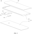
- FIG. 2 schematically shows a partial decomposition structure of the electronic device 10.
- the electronic device 10 in this embodiment of this application includes a display assembly 20, a housing 30, a mainboard 40, and an electronic component 50.
- the display assembly 20 has a display region used to display image information.
- the display assembly 20 presents image information to a user by using the display region.
- the display assembly 20 is mounted on the housing 30.
- the mainboard 40 may be connected to the housing 30, and is located in the housing 30.
- the mainboard 40 may be located between the display assembly 20 and the housing 30, so that the user does not easily observe the mainboard 40 from the exterior of the electronic device 10.
- the housing 30 includes a rear cover 31 and a frame 32.
- the rear cover 31 is connected to the frame 32.
- the frame 32 may be but is not limited to a rectangular frame.
- the mainboard 40 may be disposed in space formed by the rear cover 31 and the frame 32.
- the electronic component 50 is disposed on the mainboard 40.
- the mainboard 40 may be a printed circuit board (Printed Circuit Board, PCB).
- the electronic component 50 is welded to the mainboard 40 by using a welding process.
- the electronic component 50 includes but is not limited to a radio frequency chip (Radio Frequency Integrated Circuit, RFIC), a radio frequency power amplifier (Radio Frequency Power Amplifier, RFPA), a wireless fidelity (Wireless Fidelity, WIFI) chip, a central processing unit (Central Processing Unit, CPU), an intelligent algorithm chip, a power management chip (Power Management IC, PMIC), or an application processor (Application Processor, AP).
- the application processor may be used to carry a system on chip (System On Chip, SOC).
- the system on chip includes an image signal processing (Image Signal Processing, ISP) module. Because internal space of the electronic device 10 is relatively small, the electronic component 50 is highly integrated on the mainboard 40 to sufficiently reduce a volume of the mainboard 40 and reduce space occupation of the mainboard 40.
- ISP Image Signal Processing
- the electronic device 10 may further include another component such as a battery.
- the battery may be disposed in the housing 30.
- the battery is a structural member that can convert chemical energy into electrical energy.
- the battery is used to provide electrical energy to the electronic device 10 to ensure normal working of the electronic device 10.
- the battery may provide electrical energy to the display assembly 20, so that the display assembly 20 displays image information or completes corresponding operation instructions.
- the battery may provide electrical energy to the mainboard 40, to ensure that the electronic component 50 on the mainboard 40 works normally.
- the battery may be a lithium ion battery, such as a lithium iron phosphate battery.
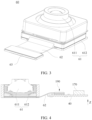
- FIG. 3 schematically shows a partial structure of a camera apparatus.
- the electronic device 10 may include a camera apparatus 60.
- the camera apparatus 60 may include a camera module 61 and a circuit board 62.
- the camera module 61 may be electrically connected to the mainboard 40 by using the circuit board 62, to implement signal interaction.
- the circuit board 62 may be but is not limited to a flexible printed circuit board (Flexible Printed Circuit Board, FPCB).
- the camera module 61 of the camera apparatus 60 may be disposed in the housing 30.
- the housing 30 has a light-transmitting hole. In an axial direction of the light-transmitting hole, a light entry part of the camera module 61 corresponds to the light-transmitting hole.
- External light may reach the light entry part through the light-transmitting hole.
- a cross-sectional shape of the light-transmitting hole may be a circle, an ellipse, or a polygon. This is not limited in this application.
- the camera apparatus 60 may be a rear-facing camera, or may be a front-facing camera. This is not limited in this application.
- the camera module 61 may include an optical imaging system 611 and an image sensor 612.
- the optical imaging system 611 may include a plurality of lenses. When the camera module 61 is used for shooting, light on an object side may be incident on a photosensitive surface of the image sensor 612 after passing through the optical imaging system 611.
- the photosensitive surface of the image sensor 612 is a surface on which light is received.
- the optical imaging system 611 has a virtual imaging plane.
- the imaging plane of the optical imaging system 611 may coincide with the photosensitive surface of the image sensor 612.
- the image sensor 612 may be a sensor that converts, into an electrical signal, an optical signal that is to be incident on the photosensitive surface.
- the image sensor 612 may be a complementary metal-oxide-semiconductor (Complementary Metal Oxide Semiconductor, CMOS) sensor or a charge coupled device (Charge coupled Device, CCD).
- CMOS Complementary Metal Oxide Semiconductor
- CCD charge coupled Device
- FIG. 4 schematically shows a partial cross-sectional structure of an electronic device in the related technology.
- the image sensor 612 of the camera module 61 may be electrically connected to a system on chip 170 on the mainboard 40 by using the circuit board 62 and a connector 190.
- the connector 190 includes two connection terminals that are plug-connected to each other.
- the connector 190 may be a board-to-board connector (Board-to-board Connectors).
- the camera apparatus 60 of the electronic device 10 When the camera apparatus 60 of the electronic device 10 performs a shooting function, interaction of a signal such as a data signal or a control signal exists between the image sensor 612, the circuit board 62, the connector 190, a wire on the mainboard 40, and an image signal processing module of the system on chip 170.
- a signal such as a data signal or a control signal
- the connector 190 has relatively large ground impedance
- the connector 190 becomes an impedance discontinuity point with a sudden change in impedance.
- the connector 190 is easily coupled to an external electromagnetic field, resulting in interference with a data signal or a control signal that is transmitted between the camera module 61 and the image signal processing module.
- the camera apparatus 60 is interfered with by a signal, and a phenomenon such as a screen artifact, stalling, or screen freezing occurs in a shooting interface.
- a phenomenon such as a screen artifact, stalling, or screen freezing occurs in a shooting interface.
- This affects shooting experience of the electronic device 10.
- the radio frequency chip or the wireless fidelity chip transmits power, a generated electromagnetic signal causes signal interference to the connector 190.
- a shielding member is disposed on the mainboard 40, and covers the exterior of a first connection terminal and a second connection terminal.
- the first connection terminal and the second connection terminal may be grounded by using the shielding member, thereby effectively reducing impedance.
- the shielding member may be used to shield the first connection terminal and the second connection terminal. Therefore, according to the electronic device 10 in this embodiment of this application, a possibility that an electromagnetic signal interferes with the first connection terminal and the second connection terminal can be reduced, thereby helping reduce a possibility that the camera apparatus 60 is interfered with by a signal, and improving shooting experience of the electronic device 10.
- FIG. 5 schematically shows a partial structure of the electronic device.
- FIG. 5 shows a top-view structure in a thickness direction Z of the mainboard 40 in FIG. 4 .
- FIG. 6 schematically shows a partial decomposition structure of the electronic device 10.
- the mainboard 40 in this embodiment of this application includes a first connection terminal 41 and a ground terminal 42.
- the first connection terminal 41 provides an adapter interface.
- the first connection terminal 41 may be electrically connected to the system on chip 170 on the mainboard 40.
- the ground terminal 42 is used for grounding.
- the camera apparatus 60 includes the camera module 61, the circuit board 62, and a second connection terminal 63.
- the camera module 61 is electrically connected to the circuit board 62.
- the second connection terminal 63 is disposed on the circuit board 62.
- the second connection terminal 63 is electrically connected to the circuit board 62.
- the circuit board 62 may be a flexible printed circuit board.
- the circuit board 62 may be of a strip-shaped structure.
- the camera module 61 is electrically connected to one end of the circuit board 62, and the second connection terminal 63 is electrically connected to the other end of the circuit board 62.
- the first connection terminal 41 is electrically connected to the second connection terminal 63.
- the first connection terminal 41 and the second connection terminal 63 are detachably connected to facilitate assembly or separation of the first connection terminal 41 and the second connection terminal 63, thereby facilitating assembly or separation of the camera apparatus 60 and the mainboard 40.
- the first connection terminal 41 is connected to the second connection terminal 63 to form a connector.
- the connector formed by the first connection terminal 41 and the second connection terminal 63 may be a board-to-board connector.
- the first connection terminal 41 and the second connection terminal 63 may be connected to each other in a plug-connected manner.
- the first connection terminal 41 and the second connection terminal 63 each have a pin, and the two connection terminals are plug-connected to each other by using respective pins (PIN pin), to implement electrical connection.
- the camera module 61 may be communicatively connected to the mainboard 40 by using the circuit board 62, the second connection terminal 63, and the first connection terminal 41, to implement interaction of a signal such as a data signal or a control signal.
- the electronic device 10 further includes a shielding member 70.
- the mainboard 40 may provide a mounting base for the shielding member 70.
- the shielding member 70 is connected to the mainboard 40.
- the shielding member 70 may be disposed to avoid the electronic component 50 on the mainboard 40.
- Accommodating space 180 (as shown in FIG. 8 ) is formed between the shielding member 70 and the mainboard 40.
- the first connection terminal 41 and the second connection terminal 63 are located in the accommodating space 180.
- the shielding member 70 is electrically connected to the ground terminal 42 of the mainboard 40, so that the shielding member 70 is grounded.
- FIG. 7 schematically shows a partial structure of the electronic device.
- FIG. 8 schematically shows a partial cross-sectional structure of the electronic device.
- the shielding member 70 includes a shielding frame 71 and a shielding cover 72 that are electrically connected.
- the shielding frame 71 is used for grounding.
- the shielding frame 71 is connected to the mainboard 40.
- the shielding frame 71 is electrically connected to the ground terminal 42 of the mainboard 40.
- the shielding cover 72 is connected to the shielding frame 71.
- the shielding cover 72 and the shielding frame 71 are detachably connected.
- the shielding cover 72 is connected to the shielding frame 71 to form an accommodating cavity having an opening. After the shielding cover 72 is assembled with the shielding frame 71, the shielding member 70 having an accommodating cavity is formed.
- the second connection terminal 63 is electrically connected to the shielding cover 72.
- the shielding frame 71 is electrically connected to the shielding cover 72, and the shielding frame 71 is electrically connected to the ground terminal 42. Therefore, the shielding cover 72 is indirectly grounded by using the shielding frame 71, and the second connection terminal 63 is indirectly grounded by using the shielding cover 72 and the shielding frame 71.
- the assembled shielding member 70 may cover the first connection terminal 41 and the second connection terminal 63, and the shielding member 70 is grounded. This helps eliminate parasitic capacitance formed between the ground terminal 42 of the mainboard 40 and the connector formed by the first connection terminal 41 and the second connection terminal 63, thereby helping reduce a possibility that an electromagnetic signal causes electromagnetic coupling interference to the first connection terminal 41 and the second connection terminal 63.
- the shielding member 70 is disposed on a periphery of the connector formed by the first connection terminal 41 and the second connection terminal 63.
- the shielding member 70 covers the connector formed by the first connection terminal 41 and the second connection terminal 63.
- the accommodating space 180 formed by connecting the shielding member 70 and the mainboard 40 may also be referred to as shielding space.
- the opening of the accommodating cavity of the shielding member 70 faces the mainboard 40.
- the accommodating space 180 includes the accommodating cavity of the shielding member 70.
- the first connection terminal 41 and the second connection terminal 63 are located in the shielding space.
- the shielding member 70 may be used to provide effective shielding for the first connection terminal 41 and the second connection terminal 63, to reduce an electromagnetic signal of another component on the outer side of the shielding member 70 or an electromagnetic signal in an environment in which the electronic device 10 is located from interfering with the first connection terminal 41 and the second connection terminal 63. This helps reduce a possibility that signal interaction between the camera module 61 and the mainboard 40 is interfered with because the first connection terminal 41 and the second connection terminal 63 are interfered with by an electromagnetic signal, thereby improving working stability of the camera apparatus 60.
- the mainboard 40 includes the first connection terminal 41 and the ground terminal 42
- the camera apparatus 60 includes the camera module 61, the circuit board 62, and the second connection terminal 63.
- the first connection terminal 41 and the second connection terminal 63 are detachably connected.
- the first connection terminal 41 is electrically connected to the second connection terminal 63.
- the camera apparatus 60 is communicatively connected to the mainboard 40, to implement signal interaction.
- the shielding member 70 is connected to the mainboard 40, and the shielding member 70 covers the exterior of the first connection terminal 41 and the second connection terminal 63.
- the shielding member 70 is electrically connected to the ground terminal 42 of the mainboard 40, to implement grounding.
- the second connection terminal 63 is electrically connected to the shielding member 70.
- the first connection terminal 41, the second connection terminal 63, the shielding cover 72, and the shielding frame 71 may be grounded by using the ground terminal 42 of the mainboard 40.
- This helps reduce ground impedance at the connector formed by the first connection terminal 41 and the second connection terminal 63, to avoid a sudden change in impedance at the connector formed by the first connection terminal 41 and the second connection terminal 63, and helps eliminate the parasitic capacitance formed between the ground terminal 42 of the mainboard 40 and the connector formed by the first connection terminal 41 and the second connection terminal 63, thereby helping reduce a possibility that an electromagnetic signal interferes with the first connection terminal 41 and the second connection terminal 63 and electromagnetic coupling occurs.
- the shielding member 70 may also effectively shield the electromagnetic signal from adversely affecting and interfering with the first connection terminal 41 and the second connection terminal 63, thereby further helping reduce a possibility that an interaction signal between the camera apparatus 60 and the mainboard 40 is interfered with.
- the shielding cover 72 and the shielding frame 71 may be welded to each other, to ensure good connection reliability and stability between the shielding cover 72 and the shielding frame 71, and reduce a possibility that the shielding cover 72 and the shielding frame 71 are separated from each other due to accidental collision of the shielding cover 72.
- the shielding cover 72 and the shielding frame 71 are detachably connected, to facilitate assembly or separation of the shielding cover 72 and the shielding frame 71.
- the first connection terminal 41 and the second connection terminal 63 are disposed between the shielding cover 72 and the mainboard 40.
- the shielding cover 72 is removed from the shielding frame 71, without a need to remove the shielding member 70 as a whole from the mainboard 40.
- the shielding cover 72 is reassembled with the shielding frame 71.
- An assembly process may be but is not limited to the following process: disposing the first connection terminal 41 on the mainboard 40; then sleeving a periphery of the first connection terminal 41 by using the shielding frame 71; then connecting the shielding frame 71 to the mainboard 40; connecting the second connection terminal 63 to the first connection terminal 41; connecting the shielding cover 72 to the shielding frame 71; and covering the first connection terminal 41 and the second connection terminal 63 by using the assembled shielding member 70.
- the shielding member 70 may be welded to the mainboard 40 by using the welding process.
- the shielding member 70 is welded to the ground terminal 42. This helps implement good grounding, and can ensure that connection strength between the shielding member 70 and the ground terminal 42 is relatively large, thereby improving connection stability between the shielding member 70 and the ground terminal 42.
- the shielding member 70 and the ground terminal 42 may be welded by using solder.
- the shielding frame 71 of the shielding member 70 is welded to the mainboard 40 by using the welding process.
- the shielding frame 71 of the shielding member 70 may be welded to the ground terminal 42.
- materials of both the shielding cover 72 and the shielding frame 71 may be conductive metal materials.
- the materials of the shielding cover 72 and the shielding frame 71 may be stainless steel.
- the electronic device 10 further includes an electronic element 150.
- the electronic element 150 is disposed on the mainboard 40.
- the electronic element 150 is disposed in the accommodating space 180.
- the electronic element 150 is spaced apart from the first connection terminal 41.
- the shielding member 70 may have a shielding effect on the electronic element 150. Therefore, when the electronic element 150 is in a working state, an electromagnetic signal transmitted by the electronic element 150 is not easily propagated to a component that is located on an outer side of the shielding member 70 and that is relatively close to the electronic element 150. This effectively reduces a possibility that the electronic element 150 causes signal interference to a neighboring component.
- the electronic element 150 may be an inductor.
- the electronic device 10 further includes an antenna.
- the housing 30 includes a rear cover 31 and a frame 32.
- the antenna may be disposed on the frame 32.
- the electronic element 150 for example, the inductor
- the inductor because the inductor is shielded by the shielding member 70, when in a working state, the inductor does not easily causes signal interference to a neighboring antenna.
- FIG. 9 schematically shows a partial structure of the electronic device.
- the shielding frame 71 may be a frame having an intermediate through hole 71a.
- the first connection terminal 41 is located in the intermediate through hole 71a.
- the shielding frame 71 may be an annular frame.
- a shape of an orthographic projection of the shielding frame 71 on the mainboard 40 may be regular, such as a rectangle or a circle.
- a shape of an orthographic projection of the shielding frame 71 on the mainboard 40 may alternatively be irregular. This is not specifically limited in this application.
- the shielding frame 71 may also have a notch, and the shielding frame 71 is disconnected and discontinuous at the notch, so that the shielding frame 71 is not of a continuous annular structure.
- the first connection terminal 41 is located in the shielding frame 71. For example, there is a distance between the first connection terminal 41 and the shielding frame 71. In the thickness direction Z of the mainboard 40, an orthographic projection of the first connection terminal 41 is located in an orthographic projection of the shielding frame 71, and the two orthographic projections do not overlap.
- the intermediate through hole 71a of the shielding frame 71 avoids the first connection terminal 41. Therefore, in a process of assembling the second connection terminal 63 with the first connection terminal 41, location interference between the shielding frame 71 and the second connection terminal 63 is avoided.
- the shielding frame 71 may be an annular frame. The shielding frame 71 is disposed around the first connection terminal 41. Therefore, in any direction, the shielding frame 71 can have a good shielding effect on the first connection terminal 41.
- the shielding frame 71 includes a bottom flange 711, a first side plate 712, and a top flange 713. Both the bottom flange 711 and the top flange 713 are connected to the first side plate 712. The bottom flange 711 and the top flange 713 separately intersect with the first side plate 712. The bottom flange 711 is electrically connected to the ground terminal 42 of the mainboard 40. For example, the bottom flange 711 may be welded to the ground terminal 42 of the mainboard 40.
- the bottom flange 711 is of an annular structure, and a shape of the ground terminal 42 of the mainboard 40 may match the bottom flange 711, that is, the ground terminal 42 may also be of an annular structure.
- a material of the ground terminal 42 may be but is not limited to copper or a copper alloy.
- An outer surface that is of the top flange 713 and that faces away from the mainboard 40 is electrically connected to an inner surface that is of the shielding cover 72 and that faces the mainboard 40.
- the shielding cover 72 may be grounded to the ground terminal 42 of the mainboard 40 by using the top flange 713, the first side plate 712, and the bottom flange 711.
- the outer surface that is of the top flange 713 and that faces away from the mainboard 40 directly abuts against the inner surface that is of the shielding cover 72 and that faces the mainboard 40, so that the top flange 713 is electrically connected to the shielding cover 72.
- the bottom flange 711 and the top flange 713 are respectively disposed at a bottom end and a top end of the first side plate 712.
- the bottom flange 711 and the top flange 713 are respectively located on two sides of the first side plate 712.
- the bottom flange 711 may be folded outward by facing away from the first connection terminal 41, and the top flange 713 may be folded inward toward the first connection terminal 41.
- an orthographic projection of the top flange 713 does not overlap an orthographic projection of the first connection terminal 41.
- the outer surface that is of the top flange 713 and that faces away from the mainboard 40 directly abuts against the inner surface that is of the shielding cover 72 and that faces the mainboard 40, so that the top flange 713 is electrically connected to the shielding cover 72.
- a width of at least a part of the top flange 713 is greater than a width of the bottom flange 711.
- the width of the top flange 713 and the width of the bottom flange 711 refer to sizes measured in a direction perpendicular to the thickness direction Z of the mainboard 40.
- a manner of setting the width of at least a part of the top flange 713 to be relatively large helps increase a contact area between the shielding cover 72 and the shielding frame 71, to effectively compensate for the contact area between the shielding cover 72 and the shielding frame 71, and reduce a possibility that the contact area does not meet a requirement because the surfaces that are of the shielding cover 72 and the shielding frame 71 and that are used for contact are uneven.
- the bottom flange 711 is set to have a relatively small width. This can help reduce an orthographic projection area of the bottom flange 711 on the mainboard 40 when connection strength between the bottom flange 711 and the mainboard 40 is met, thereby reducing space occupation of the mainboard 40 by the bottom flange 711, and reducing a possibility that a region that is of the mainboard 40 and in which the electronic component 50 can be disposed is reduced because the bottom flange 711 occupies excessive space on the mainboard 40.
- the width of the top flange 713 at any location is greater than the width of the bottom flange 711.
- a width of a partial region of the top flange 713 is greater than a width of a remaining region thereof.
- the width of the top flange 713 may be set to be relatively small.
- the width of the top flange 713 may be set to be relatively large. Therefore, when there is no location interference between the top flange 713 and the first connection terminal 41, the top flange 713 as a whole may be set to have a relatively large width size, thereby facilitating a relatively large contact area between the shielding cover 72 and the shielding frame 71.
- a blank for processing and manufacturing the shielding frame 71 is a flat sheet.
- the blank is stamped by using a stamping process, to obtain the shielding frame 71 with the bottom flange 711, the first side plate 712, and the top flange 713 through stamping.
- shaping processing is performed on the shielding frame 71 to sufficiently release internal stress of the shielding frame 71.
- the shielding cover 72 and the shielding frame 71 are snap-fitted with each other.
- the shielding cover 72 and the shielding frame 71 are in contact with and pressed against each other at a snap-fit location, so that good electrical connection can also be maintained between the shielding cover 72 and the shielding frame 71 at the snap-fit location.
- a snap-in part 80 is disposed on one of the shielding cover 72 and the shielding frame 71, and a fitting part 90 is disposed on the other thereof.
- the shielding cover 72 and the shielding frame 71 may be snap-fitted with each other by using the snap-in part 80 and the fitting part 90.
- a snap-fit manner is used for the shielding cover 72 and the shielding frame 71, to facilitate quick assembly or separation of the shielding cover 72 and the shielding frame 71, and improve assembly or separation working efficiency.
- the snap-in part 80 and the fitting part 90 that are snap-fitted with each other may be pressed against and fitted with each other, so that good electrical connection can also be maintained between the shielding cover 72 and the shielding frame 71 at a location at which the snap-in part 80 is snap-fitted with the fitting part 90.
- the snap-in part 80 may be limited by the fitting part 90, so that a stable connection state can be maintained between the snap-in part 80 and the fitting part 90.
- the snap-in part 80 is not easily detached from the fitting part 90, thereby reducing a possibility that a shielding failure of the shielding member 70 is caused because the shielding cover 72 and the shielding frame 71 are separated from each other due to accidental collision.
- the snap-in part 80 may be a protruding part
- the fitting part 90 may be a blind hole or a through hole.
- the shielding cover 72 may be of an integrally formed structure.
- the shielding frame 71 may be of an integrally formed structure. Processing may be directly performed on one of the shielding cover 72 and the shielding frame 71 to form the snap-in part 80, and processing may be directly performed on the other thereof to form the fitting part 90. Therefore, structures of the shielding cover 72 and the shielding frame 71 may maintain good integrity.
- an additional snap-fit assembly including the snap-in part 80 and the fitting part 90 does not need to be disposed between the shielding cover 72 and the shielding frame 71. This helps reduce a quantity of used parts, and reduces assembly operations that one of the shielding cover 72 and the shielding frame 71 needs to be assembled with the snap-in part 80 and the other thereof needs to be assembled with the fitting part 90.
- the outer surface that is of the top flange 713 and that faces away from the mainboard 40 directly abuts against the inner surface that is of the shielding cover 72 and that faces the mainboard 40.
- the shielding cover 72 and the shielding frame 71 are snap-fitted with each other, so that connection reliability between the shielding cover 72 and the shielding frame 71 can be improved.
- the shielding cover 72 effectively presses against the top flange 713, to ensure that a good fitted and contact state is maintained between the shielding cover 72 and the top flange 713, and reduces a possibility that poor contact occurs between the shielding cover 72 and the top flange 713 due to loosening of the shielding cover 72 and the shielding frame 71, thereby reducing a possibility that a passive inter-modulation (Passive Inter-Modulation, PIM) problem and a spurious emission (RSE) problem are generated due to poor contact.
- PIM passive inter-modulation
- RSE spurious emission
- the shielding frame 71 may include the first side plate 712, the bottom flange 711, and the top flange 713 that are connected to each other.
- the shielding cover 72 and the first side plate 712 are snap-fitted with each other.
- a snap-fit manner is used for the shielding cover 72 and the first side plate 712, to facilitate quick assembly or separation of the shielding cover 72 and the shielding frame 71, and improve assembly or separation working efficiency.
- the snap-in part 80 is disposed on one of the shielding cover 72 and the first side plate 712, and the fitting part 90 is disposed on the other thereof.
- the snap-in part 80 is snap-fitted with the fitting part 90.
- the outer surface that is of the top flange 713 of the shielding frame 71 and that faces away from the mainboard 40 is electrically connected to an inner surface that is of a top plate and that faces the mainboard 40.
- the shielding cover 72 may include a top plate 721 and a second side plate 722 that are connected to each other.
- the second side plate 722 and the top plate 721 of the shielding cover 72 intersect each other, and there is a predetermined included angle between the second side plate 722 and the top plate 721.
- the included angle between the second side plate 722 and the top plate 721 may be 90°.
- a blank for processing and manufacturing the shielding cover 72 is a flat sheet. First, the blank is stamped by using a stamping process, to obtain the shielding cover 72 with the second side plate 722 and the top plate 721 through stamping. Next, shaping processing is performed on the shielding cover 72 to sufficiently release internal stress of the shielding cover 72.
- the snap-in part 80 is disposed on one of the first side plate 712 of the shielding frame 71 and the second side plate 722 of the shielding cover 72, and the fitting part 90 is disposed on the other thereof.
- the first connection terminal 41 and the second connection terminal 63 are disposed between the top plate 721 of the shielding cover 72 and the mainboard 40.
- the first connection terminal 41 and the second connection terminal 63 are disposed on a side that is of the top plate 721 of the shielding cover 72 and that faces the mainboard 40.
- the second side plate 722 of the shielding cover 72 may be elastically deformed. After the snap-in part 80 is snapped into the fitting part 90, the snap-in part 80 and the fitting part 90 are pressed against and fitted with each other under the action of an elastic recovery force of the second side plate 722. In addition, the top flange 713 of the shielding frame 71 and the top plate 721 of the shielding cover 72 are pressed against and fitted with each other.
- the snap-in part 80 is disposed on the shielding cover 72, and the fitting part 90 is disposed on the shielding frame 71.
- the fitting part 90 is disposed on the first side plate 712 of the shielding frame 71, and the snap-in part 80 is disposed on the second side plate 722 of the shielding cover 72.
- the fitting part 90 on the first side plate 712 of the shielding frame 71 has an opening facing away from the intermediate through hole 71a, that is, the fitting part 90 has an opening disposed outward.
- the snap-in part 80 on the second side plate 722 of the shielding cover 72 protrudes toward the accommodating space 180. After the shielding cover 72 is assembled with the shielding frame 71, the second side plate 722 of the shielding cover 72 is located on the outer side of the first side plate 712 of the shielding frame 71, and is in an externally visible state.
- the snap-in part 80 on the second side plate 722 is located in the fitting part 90.
- the second side plate 722 may abut against the first side plate 712, so that the first side plate 712 is in contact with the second side plate 722.
- the first side plate 712 of the shielding frame 71 may have a plurality of outer side surfaces.
- the shielding cover 72 may include a plurality of second side plates 722.
- the plurality of second side plates 722 are separately independent. There is a distance between two adjacent second side plates 722, so that a gap is formed between two adjacent second side plates 722.
- the second side plates 722 are disposed independently. Therefore, in a snap-fit process, when any one of the second side plates 722 is deformed, none of the other second side plates 722 is pulled.
- the snap-in part 80 may be disposed on each second side plate 722.
- the fitting part 90 is disposed at a location that is on the first side plate 712 and that corresponds to the second side plate 722.
- FIG. 10 schematically shows a partial structure of the electronic device.
- the first side plate 712 of the shielding frame 71 has a first outer side surface 7121, a second outer side surface 7122, a third outer side surface 7123, and a fourth outer side surface 7124 that are connected to each other.
- the circuit board 62 of the camera apparatus 60 may pass through between the shielding cover 72 and the shielding frame 71.
- the circuit board 62 of the camera apparatus 60 corresponds to the first outer side surface 7121.
- the third outer side surface 7123 may be a stepped surface.
- the shielding cover 72 may include five second side plates 722.
- the first outer side surface 7121 corresponds to one second side plate 722, the second side plate 722 is close to the fourth outer side surface 7124, and there is a distance between the second side plate 722 and the circuit board 62 of the camera apparatus 60.
- the second outer side surface 7122 and the fourth outer side surface 7124 each correspond to one second side plate 722.
- the third outer side face 7123 corresponds to two second side faces 722.
- One second side plate 722 close to the second outer side surface 7122 is relatively close to the first outer side surface 7121, and one second side plate 722 close to the fourth outer side surface 7124 is relatively away from the first outer side surface 7121.
- the outer surface that is of the top flange 713 and that faces away from the mainboard 40 directly abuts against the inner surface that is of the top plate 721 and that faces the mainboard 40, so that the top flange 713 is electrically connected to the top plate 721.
- one end of the circuit board 62 is connected to the camera module 61, and the other end thereof is provided with the second connection terminal 63.
- the second connection terminal 63 is disposed on an end part that is of the circuit board 62 and that is away from the camera module 61.
- FIG. 11 schematically shows a partial cross-sectional structure of the electronic device.
- FIG. 12 is an enlarged view of a location M in FIG. 11 .
- the shielding member 70 includes an avoidance hole 130.
- the end part that is of the circuit board 62 and on which the second connection terminal 63 is disposed passes through the avoidance hole 130, and is located within the accommodating space 180 together with the second connection terminal 63.
- the avoidance hole 130 may be formed between the shielding cover 72 and the shielding frame 71.
- the circuit board 62 of the camera apparatus 60 passes through the avoidance hole 130.
- the circuit board 62 is located above the shielding frame 71.
- the avoidance hole 130 corresponds to the first outer side surface 7121 of the first side plate 712.
- the circuit board 62 of the camera apparatus 60 corresponds to the first outer side surface 7121 of the first side plate 712.
- a surface that is of the second connection terminal 63 and that faces away from the first connection terminal 41 is bonded to the shielding cover 72 by using a conductive adhesive, so that the second connection terminal 63 is electrically connected to the shielding cover 72.
- An assembly manner may be but is not limited to the following: After the second connection terminal 63 is assembled with the first connection terminal 41, the conductive adhesive is disposed on the surface that is of the second connection terminal 63 and that faces away from the first connection terminal 41. Then, the shielding cover 72 is snap-fitted with the shielding frame 71. After the shielding cover 72 is assembled with the shielding frame 71, the shielding cover 72 is bonded to the conductive adhesive.
- the electronic device 10 further includes a reinforcement member 100.
- the reinforcement member 100 is located in the accommodating space 180. At least a part of the reinforcement member 100 is disposed on a side that is of the second connection terminal 63 and that faces away from the first connection terminal 41.
- the shielding member 70 may apply compressive stress to the reinforcement member 100 toward the second connection terminal 63, to ensure connection reliability and stability between the first connection terminal 41 and the second connection terminal 63, and reduce a possibility that the second connection terminal 63 is removed from the first connection terminal 41 and is in a disconnected state.
- the reinforcement member 100 may provide protection for the second connection terminal 63, to effectively avoid a case in which structural damage occurs in the second connection terminal 63 because the second connection terminal 63 is impacted by an external force.
- the reinforcement member 100 may isolate the second connection terminal 63 from the shielding member 70, to reduce a possibility that a structure of the second connection terminal 63 is damaged because the shielding member 70 directly applies compressive stress to the second connection terminal 63.
- the reinforcement member 100 may be connected to the second connection terminal 63.
- the reinforcement member 100 is of a conductive structure.
- the reinforcement member 100 is electrically connected to the second connection terminal 63.
- the reinforcement member 100 is electrically connected to the shielding cover 72. Therefore, the second connection terminal 63 is electrically connected to the ground terminal 42 of the mainboard 40 by using the reinforcement member 100, the shielding cover 72, and the shielding frame 71, to implement indirect grounding.
- the structure of the shielding member 70 may be replaced by a pressing steel sheet.
- a strip-shaped pressing steel sheet is disposed above the reinforcement member 100 in the thickness direction Z of the mainboard 40.
- the pressing steel sheet is used to press the reinforcement member 100 and the second connection terminal 63 in the thickness direction Z of the mainboard 40.
- Grounding to the mainboard 40 may be implemented by using two end parts of the pressing steel sheet.
- a fastener such as a screw may be used to connect the end part of the pressing steel sheet to the mainboard 40 to implement grounding.
- a ground region between the pressing steel sheet and the mainboard 40 is relatively small, and a shielding region of the pressing steel sheet for the first connection terminal 41 and the second connection terminal 63 is also relatively small.
- a ground region between the shielding member 70 and the mainboard 40 is relatively large, and the shielding member 70 may cover the first connection terminal 41 and the second connection terminal 63, so that the shielding member 70 can effectively improve a shielding effect.
- a relatively large contact area between the reinforcement member 100 and the shielding member 70 helps implement a relatively large electrical connection area between the reinforcement member 100 and the shielding member 70 and reduce impedance, so that a manner of disposing both the shielding member 70 and the reinforcement member 100 can effectively improve a shielding effect.
- a material of the reinforcement member 100 may be a metal material.
- the material of the reinforcement member 100 may be steel, for example, may be stainless steel.
- the reinforcement member 100 may be a steel sheet.
- At least one of the second connection terminal 63 and the top plate 721 of the shielding cover 72 may be bonded to the reinforcement member 100.
- the reinforcement member 100 may be connected to the second connection terminal 63 through bonding.
- the reinforcement member 100 may be bonded to the second connection terminal 63 by using a conductive adhesive layer, to implement electrical connection between the reinforcement member 100 and the second connection terminal 63.
- the shielding cover 72 of the shielding member 70 directly abuts against the reinforcement member 100.
- the shielding cover 72 of the shielding member 70 is in direct contact with the reinforcement member 100 to implement electrical connection, so that there is no need to dispose an additional structural member for implementing electrical connection between the shielding member 70 and the reinforcement member 100. This helps reduce a quantity of used parts and assembly operations.
- the shielding cover 72 is located on a side that is of the reinforcement member 100 and that faces away from the mainboard 40. After the shielding cover 72 is assembled with the shielding frame 71, the shielding cover 72 may directly abut against the reinforcement member 100.
- the shielding cover 72 may apply compressive stress to the reinforcement member 100 and the second connection terminal 63, to ensure connection stability between the second connection terminal 63 and the first connection terminal 41.
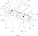
- FIG. 13 schematically shows a partial cross-sectional structure of the electronic device.
- the shielding member 70 has an insulating layer 140.
- An outer surface of the shielding cover 72 may be provided with the insulating layer 140.
- the insulating layer 140 disposed on the shielding cover 72 may help maintain a good insulation and isolation state between the shielding cover 72 and another conductive structural member. If the shielding cover 72 is not provided with the insulating layer 140, there is a case in which the shielding cover 72 is electrically connected to another conductive structural member.
- the outer surface of the shielding cover 72 may be provided with insulating paint.
- the insulating paint is cured to form the insulating layer 140.
- the insulating paint may be sprayed on the outer surface of the shielding cover 72 through spraying.
- FIG. 14 schematically shows a partial cross-sectional structure of the electronic device.
- the electronic device 10 further includes a conductive member 110.
- the conductive member 110 is disposed between the shielding cover 72 of the shielding member 70 and the reinforcement member 100.
- the conductive member 110 may implement electrical connection between the shielding member 70 and the reinforcement member 100.
- the shielding cover 72 and the reinforcement member 100 may jointly press against the conductive member 110, to ensure good contact between the conductive member 110 and each of the shielding member 70 and the reinforcement member 100, and maintain stability of an electrical connection state between the conductive member 110 and each of the shielding member 70 and the reinforcement member 100.
- the conductive member 110 may be of a flexible structure, and has compressible and deformable performance.
- the shielding cover 72 of the shielding member 70 and the reinforcement member 100 may jointly press against the conductive member 110.
- the conductive member 110 may be compressed and deformed. Therefore, when a surface of at least one of the shielding cover 72 of the shielding member 70 and the reinforcement member 100 is uneven, the conductive member 110 may perform compensation through deformation thereof, to ensure that a close fitted and contact state is maintained between the shielding cover 72 of the shielding member 70 and the conductive member 110 and between the reinforcement member 100 and the conductive member 110. In this way, a good electrical connection state is maintained between the shielding cover 72 of the shielding member 70 and the reinforcement member 100, to help reduce impedance.
- the conductive member 110 may be a conductive fabric or a conductive adhesive layer.
- the reinforcement member 100 is capacitively coupled to the shielding cover 72 of the shielding member 70, thereby implementing an equivalent electrical connection effect between the reinforcement member 100 and the shielding member 70.
- a capacitor with relatively large capacitance may be equivalently formed between the reinforcement member 100 and the shielding cover 72 of the shielding member 70, so that an electrical signal can be coupled from one of the reinforcement member 100 and the shielding member 70 to the other thereof.
- the reinforcement member 100 is not in direct contact with the shielding cover 72, so that a case in which poor contact occurs between the shielding cover 72 and the reinforcement member 100 can be avoided, thereby reducing a possibility that a passive inter-modulation (Passive Inter-Modulation, PIM) problem and a spurious emission (RSE) problem are generated due to poor contact.
- PIM passive inter-modulation
- RSE spurious emission
- FIG. 15 schematically shows a partial cross-sectional structure of the electronic device.
- the electronic device 10 further includes a high dielectric layer 120.
- the high dielectric layer 120 is disposed between the shielding cover 72 of the shielding member 70 and the reinforcement member 100.
- the shielding cover 72 of the shielding member 70 and the reinforcement member 100 may jointly compress the high dielectric layer 120.
- the shielding member 70, the reinforcement member 100, and the high dielectric layer 120 form a capacitive coupling.
- the high dielectric layer 120 is of a membrane structure with a relatively high dielectric constant.
- the high dielectric layer 120 may be used as an insulating medium, so that the reinforcement member 100 can be isolated from the shielding member 70.
- the reinforcement member 100 and the shielding cover 72 of the shielding member 70 each form a coupling surface with a corresponding region of the high dielectric layer 120.
- capacitance calculation formula when a distance between the reinforcement member 100 and the shielding cover 72 of the shielding member 70 and an area of the coupling surface are unchanged, if a dielectric constant of an insulating medium between the reinforcement member 100 and the shielding cover 72 of the shielding member 70 is larger, capacitance of an equivalently formed capacitor is larger.
- capacitance of a capacitor indicates smaller capacitive impedance thereof.
- the capacitive impedance is equivalent impedance.
- the shielding member 70 and the reinforcement member 100 each are in non-electrical contact with the high dielectric layer 120. There is no problem of poor contact in the capacitive coupling manner. Therefore, there is no requirement on stability of contact resistance between the high dielectric layer 120 and each of the shielding member 70 and the reinforcement member 100, so that surface processing such as nickel plating and gold plating does not need to be performed on the shielding member 70 and the reinforcement member 100.
- a location for disposing the high dielectric layer 120 may be freely and flexibly selected based on a design requirement.
- the high-frequency electrical signal may be released to the shielding member 70 through capacitive coupling between the reinforcement member 100 and the shielding member 70.
- the high dielectric layer 120 may have good elasticity, and therefore can be applied to narrow space.
- a resilience capability of the high dielectric layer 120 may be used to absorb an assembly tolerance and a machining tolerance of the shielding member 70 and the reinforcement member 100. This ensures that each of the shielding member 70 and the reinforcement member 100 is in a good pressing state with the high dielectric layer 120.
- the high dielectric layer 120 may include an elastomer and a magnesium powder or an aluminum powder that is disposed in the elastomer.
- a material of the elastomer may be plastic.
- the high dielectric layer 120 may include a wave-absorbing material, so that the high dielectric layer 120 can absorb and attenuate a spatially incident electromagnetic signal, to reduce or eliminate a reflected electromagnetic signal, and help reduce interference caused by an unwanted electromagnetic signal.
- the wave-absorbing material of the high dielectric layer 120 may include an iron-silicon aluminum material.
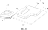
- FIG. 16 schematically shows a partial structure of the electronic device.
- An shown in FIG. 16 unlike the foregoing embodiment in which the shielding member 70 includes the shielding frame 71 and the shielding cover 72, the shielding member 70 in this embodiment is of an integrally formed structure.
- the shielding member 70 is connected to the mainboard 40.
- the shielding member 70 is welded to the mainboard 40.
- Accommodating space is formed between the shielding member 70 and the mainboard 40.
- the first connection terminal 41 and the second connection terminal 63 are located in the accommodating space.
- the shielding member 70 is electrically connected to the ground terminal 42.
- the second connection terminal 63 is electrically connected to the shielding member 70.
- the shielding member 70 includes a top wall 70a and a side wall 70b.
- the side wall 70b is connected to the mainboard 40.
- the side wall 70b is electrically connected to the ground terminal 42 of the mainboard 40.
- the shielding member 70 is welded to the ground terminal 42.
- the top wall 70a is electrically connected to the second connection terminal 63.
- the first connection terminal 41, the second connection terminal 63, the top wall 70a, and the side wall 70b may be grounded by using the ground terminal 42 of the mainboard 40.
- the side wall 70b may be of an annular structure.
- the side wall 70b of the shielding member 70 is disposed around the first connection terminal 41. Therefore, in any direction, the shielding member 70 can have a good shielding effect on the first connection terminal 41.
- a shape of the side wall 70b may be regular, such as a rectangle or a circle.
- a shape of the side wall 70b may alternatively be irregular. This is not specifically limited in this application.
- the side wall 70b may also have a notch, and the side wall 70b is disconnected and discontinuous at the notch, so that the side wall 70b is not of a continuous annular structure.
- a surface that is of the second connection terminal 63 and that faces away from the first connection terminal 41 is bonded to the top wall 70a of the shielding member 70 by using a conductive adhesive, so that the second connection terminal 63 is electrically connected to the top wall 70a of the shielding member 70.
- An assembly manner may be but is not limited to the following: After the second connection terminal 63 is assembled with the first connection terminal 41, the conductive adhesive is disposed on the surface that is of the second connection terminal 63 and that faces away from the first connection terminal 41. Then, the shielding member 70 is assembled with the mainboard 40. After the shielding member 70 is assembled with the mainboard 40, the top wall 70a of the shielding member 70 is bonded to the conductive adhesive.
- the electronic device 10 further includes a reinforcement member 100.
- the reinforcement member 100 is disposed on a side that is of the second connection terminal 63 and that faces away from the first connection terminal 41.
- the reinforcement member 100 is of a conductive structure.
- the reinforcement member 100 is electrically connected to the second connection terminal 63.
- the reinforcement member 100 is electrically connected to the top wall 70a of the shielding member 70.
- the reinforcement member 100 may provide protection for the second connection terminal 63, to effectively avoid a case in which structural damage occurs in the second connection terminal 63 because the second connection terminal 63 is impacted by an external force.
- the shielding member 70 may apply compressive stress to the reinforcement member 100 toward the second connection terminal 63, to ensure connection reliability and stability between the first connection terminal 41 and the second connection terminal 63, and reduce a possibility that the second connection terminal 63 is removed from the first connection terminal 41 and is in a disconnected state.
- the top wall 70a of the shielding member 70 directly abuts against the reinforcement member 100.
- the top wall 70a of the shielding member 70 is in direct contact with the reinforcement member 100 to implement electrical connection, so that there is no need to dispose an additional structural member for implementing electrical connection between the shielding member 70 and the reinforcement member 100. This helps reduce a quantity of used parts and assembly operations.
- the top wall 70a of the shielding member 70 is located on a side that is of the reinforcement member 100 and that faces away from the mainboard 40. After the shielding member 70 is assembled with the mainboard 40, the top wall 70a of the shielding member 70 may directly abut against the reinforcement member 100.
- the top wall 70a of the shielding member 70 may apply compressive stress to the reinforcement member 100 and the second connection terminal 63, to ensure connection stability between the second connection terminal 63 and the first connection terminal 41.
- the electronic device 10 further includes a conductive member 110.
- the conductive member 110 is disposed between the top wall 70a of the shielding member 70 and the reinforcement member 100.
- the conductive member 110 electrically connects the top wall 70a of the shielding member 70 and the reinforcement member 100.
- the conductive member 110 is disposed between the top wall 70a of the shielding member 70 and the reinforcement member 100.
- the conductive member 110 may implement electrical connection between the shielding member 70 and the reinforcement member 100.
- the top wall 70a of the shielding member 70 and the reinforcement member 100 may jointly press against the conductive member 110, to ensure good contact between the conductive member 110 and each of the shielding member 70 and the reinforcement member 100, and maintain stability of an electrical connection state between the conductive member 110 and each of the shielding member 70 and the reinforcement member 100.
- the conductive member 110 may be of a flexible structure, and has compressible and deformable performance. The conductive member 110 may be compressed and deformed.
- the conductive member 110 may perform compensation through deformation thereof, to ensure that a close fitted and contact state is maintained between the shielding member 70 and the conductive member 110 and between the reinforcement member 100 and the conductive member 110. In this way, a good electrical connection state is maintained between the shielding member 70 and the reinforcement member 100, to help reduce impedance.
- the conductive member 110 may be a conductive fabric or a conductive adhesive layer.
- the reinforcement member 100 is capacitively coupled to the top wall 70a of the shielding member 70, thereby implementing an equivalent electrical connection effect between the reinforcement member 100 and the shielding member 70.
- a capacitor with relatively large capacitance may be equivalently formed between the reinforcement member 100 and the top wall 70a of the shielding member 70, so that an electrical signal can be coupled from one of the reinforcement member 100 and the shielding member 70 to the other thereof.
- the reinforcement member 100 is not in direct contact with the shielding member 70, so that a case in which poor contact occurs between the shielding member 70 and the reinforcement member 100 can be avoided, thereby reducing a possibility that a passive inter-modulation (Passive Inter-Modulation, PIM) problem and a spurious emission (RSE) problem are generated due to poor contact.
- PIM passive inter-modulation
- RSE spurious emission
- the electronic device 10 further includes a high dielectric layer 120.
- the high dielectric layer 120 is disposed between the reinforcement member 100 and the top wall 70a of the shielding member 70.
- the top wall 70a of the shielding member 70 and the reinforcement member 100 may jointly compress the high dielectric layer 120.
- the shielding member 70, the reinforcement member 100, and the high dielectric layer 120 form a capacitive coupling.
- the shielding member 70 and the reinforcement member 100 each are in non-electrical contact with the high dielectric layer 120. There is no problem of poor contact in the capacitive coupling manner. Therefore, there is no requirement on stability of contact resistance between the high dielectric layer 120 and each of the shielding member 70 and the reinforcement member 100, so that surface processing such as nickel plating and gold plating does not need to be performed on the shielding member 70 and the reinforcement member 100.
- a location for disposing the high dielectric layer 120 may be freely and flexibly selected based on a design requirement.
- the shielding member 70 has an avoidance hole 130.
- the circuit board 62 passes through the avoidance hole 130.
- an outer surface of the shielding member 70 is provided with an insulating layer 140.
- the insulating layer 140 disposed on the shielding member 70 may help maintain a good insulation and isolation state between the shielding member 70 and another conductive structural member. If the shielding member 70 is not provided with the insulating layer 140, there is a case in which the shielding member 70 is electrically connected to another conductive structural member. If there is poor contact between the shielding member 70 and another conductive structural member, there is a possibility that a passive inter-modulation (Passive Inter-Modulation, PIM) problem and a spurious emission (RSE) problem are generated between the shielding member 70 and the another conductive structural member.
- PIM passive inter-modulation
- RSE spurious emission
- FIG. 17 schematically shows a partial structure of the electronic device.
- the electronic device 10 may include one or more camera apparatuses 60. For each camera apparatus 60, a corresponding shielding member 70 may be disposed in any manner in the foregoing embodiments.
- the electronic device 10 further includes an antenna 160.
- the housing 30 includes a rear cover 31 and a frame 32. The rear cover 31 may be connected to the frame 32.
- the antenna 160 is disposed on the frame 32.
- the antenna 160 is disposed on an inner wall that is of the frame 32 and that faces the mainboard 40.
- the first connection terminal 41, the second connection terminal 63, and the shielding member 70 are disposed close to the antenna 160.
- the first connection terminal 41, the second connection terminal 63, and the shielding member 70 may be disposed in an edge region of the mainboard 40, so that the edge region of the mainboard 40 can be effectively used, to improve utilization of the mainboard 40.
- the shielding member 70 may provide effective shielding for the first connection terminal 41 and the second connection terminal 63. Therefore, when the antenna 160 is in a working state of radiating a wireless signal, an electromagnetic signal generated by the antenna 160 does not easily interfere with the first connection terminal 41 and the second connection terminal 63, thereby reducing a possibility that the antenna 160 adversely affects the camera apparatus 60 when the camera apparatus 60 performs a shooting function.
- an electronic element 150 is disposed on the mainboard 40.
- the electronic element 150 is disposed in the accommodating space 180.
- the shielding member 70 may have a shielding effect on the electronic element 150.
- an electromagnetic signal transmitted by the electronic element 150 is not easily propagated to the antenna 160 that is located on an outer side of the shielding member 70 and that is relatively close to the electronic element 150. This effectively reduces a possibility that the electronic element 150 causes signal interference to the antenna 160.
- Table 1 Antenna frequency band Isolation N1/N3/B39 No shielding member 70 -41.2 dB The shielding member 70 is electrically connected to the reinforcement member 100. -50.7 dB N41/WIFI2.4GHz No shielding member 70 -40.2 dB The shielding member 70 is electrically connected to the reinforcement member 100. -50.1 dB
- a working frequency band of the antenna 160 may support an N1 frequency band, an N3 frequency band, and a B39 frequency band.
- the shielding member 70 is not disposed on an exterior of the connector formed by the first connection terminal 41 and the second connection terminal 63, isolation between the antenna 160 and the connector formed by the first connection terminal 41 and the second connection terminal 63 may be -41.2 dB.
- the shielding member 70 is disposed on an exterior of the connector formed by the first connection terminal 41 and the second connection terminal 63 in this application. Therefore, when the antenna 160 works in these frequency bands, isolation between the antenna 160 and the connector may be -50.7 dB, so that isolation can be increased. Therefore, the isolation between the antenna 160 and the connector meets an isolation requirement, thereby reducing a possibility of signal interference.
- the camera apparatus 60 may be a rear-facing camera of the electronic device 10.
- isolation is used to quantitatively represent strength of electromagnetic coupling in a unit of dB.
- the working frequency band of the antenna 160 may support an N41 frequency band and a WIFI2.4 GHz frequency band.
- the shielding member 70 is not disposed on an exterior of the connector formed by the first connection terminal 41 and the second connection terminal 63, isolation between the antenna 160 and the connector formed by the first connection terminal 41 and the second connection terminal 63 may be -40.2 dB.
- the shielding member 70 is disposed at the connector formed on an exterior of the first connection terminal 41 and the second connection terminal 63 in this application. Therefore, when the antenna 160 works in these frequency bands, isolation between the antenna 160 and the connector may be -50.1 dB, so that isolation can increased. Therefore, the isolation between the antenna 160 and the connector meets an isolation requirement, thereby reducing a possibility of signal interference.
- the shielding member 70 is not disposed on an exterior of the connector formed by the first connection terminal 41 and the second connection terminal 63.
- a maximum value of electric field strength measurement values at locations of the first connection terminal 41 and the second connection terminal 63 may be 42 dB V/m.
- the shielding member 70 is disposed on an exterior of the connector formed by the first connection terminal 41 and the second connection terminal 63 in this application.
- a maximum value of electric field strength measurement values at locations of the first connection terminal 41 and the second connection terminal 63 may be 26 dB V/m, so that an optimization of 16 dB V/m is relatively achieved. Therefore, the shielding member 70 is disposed, so that the first connection terminal 41 and the second connection terminal 63 can be effectively protected, thereby reducing signal interference.
- FIG. 18 schematically shows a partial cross-sectional structure of the electronic device.
- the electronic device 10 further includes a metal bracket 200.
- the mainboard 40 may be connected to the metal bracket 200.
- the metal bracket 200 is used to provide support and a mounting base for the mainboard 40.
- a partial region of the metal bracket 200 may be located on one side of the shielding member 70.
- the shielding member 70 may be located between the mainboard 40 and the metal bracket 200.
- the shielding member 70 is grounded and covers the exterior of the connector formed by the first connection terminal 41 and the second connection terminal 63.
- the shielding member 70 may effectively isolate the metal bracket 200 and the connector formed by the first connection terminal 41 and the second connection terminal 63, thereby reducing a possibility of electromagnetic signal interference on the connector formed by the first connection terminal 41 and the second connection terminal 63 because the metal bracket 200 is disposed.
- the outer surface of the shielding member 70 may have the insulating layer 140, so that an insulation and isolation state is maintained between the metal bracket 200 and the shielding member 70, and no electrical connection occurs between the metal bracket 200 and the shielding member 70.
- the terms “mount”, “communicate”, and “connect” should be understood in a broadest sense, for example, may be a fixed connection, an indirect connection by using an intermediate medium, or a connection between interiors of two elements or an interaction relationship between the two elements.
- the terms “mount”, “communicate”, and “connect” should be understood in a broadest sense, for example, may be a fixed connection, an indirect connection by using an intermediate medium, or a connection between interiors of two elements or an interaction relationship between the two elements.
- a process, a method, a system, a product, or a device that includes a series of steps or units is not necessarily limited to those steps or units that are clearly listed, but may include other steps or units that are not clearly listed or are inherent to the process, method, product, or device.
- a plurality of in this specification means two or more.
- the term “and/or” is merely used to describe an association relationship between associated objects, and indicates that three relationships may exist.
- a and/or B may indicate the following three cases: Only A exists, both A and B exist, and only B exists.
- the character "/" in this specification usually indicates an "or” relationship between associated objects. In a formula, the character "/" indicates that the associated objects are in a "division" relationship.
- sequence numbers of the foregoing processes do not mean execution sequences.
- the execution sequences of the processes should be determined according to functions and internal logic of the processes, and should not be construed as any limitation on the implementation processes of the embodiments of this application.
Landscapes
- Engineering & Computer Science (AREA)
- Microelectronics & Electronic Packaging (AREA)
- Multimedia (AREA)
- Signal Processing (AREA)
- Shielding Devices Or Components To Electric Or Magnetic Fields (AREA)
- Camera Bodies And Camera Details Or Accessories (AREA)
- Studio Devices (AREA)
Abstract
Description
- This application claims priority to
Chinese Patent Application No. 202310120762.4, filed with the China National Intellectual Property Administration on February 2, 2023 - Embodiments of this application relate to the field of terminal technologies, and in particular, to an electronic device and a shielding member.
- With explosive growth of electronic devices such as smartphones or tablet computers, the electronic device has more functions. Because people expect that the electronic device can meet more function requirements, the electronic device can implement more functions. For example, the electronic device includes a camera apparatus. People expect that camera performance of the electronic device is increasingly high, to obtain a high-resolution image. The camera apparatus includes a camera module, for example, a rear-facing camera module. The camera module is configured to photograph a selected target and form corresponding image information. The camera module includes a light entry part configured to receive light. External light may enter the camera module through the light entry part. The camera module may be electrically connected to a mainboard. For example, the camera module may be electrically connected to the mainboard by using a circuit board, to implement signal interaction. However, when the electronic device performs a shooting function, there is a case in which the camera apparatus is interfered with by a signal. Consequently, a phenomenon such as a screen artifact, stalling, or screen freezing occurs in a shooting interface. This affects shooting experience of the electronic device.
- Embodiments of this application provide an electronic device and a shielding member, so as to reduce a possibility that shooting experience is affected because a camera apparatus is interfered with by a signal.
- A first aspect of this application provides an electronic device, where the electronic device includes a mainboard, a camera apparatus, and a shielding member.
- The mainboard includes a first connection terminal and a ground terminal. The camera apparatus includes a camera module, a circuit board, and a second connection terminal. The camera module is electrically connected to the circuit board. The second connection terminal is electrically connected to the circuit board. The first connection terminal is electrically connected to the second connection terminal. Accommodating space is formed between the shielding member and the mainboard. The first connection terminal and the second connection terminal are located in the accommodating space. The shielding member includes a shielding frame and a shielding cover that are electrically connected. The shielding frame is connected to the mainboard. The shielding frame is electrically connected to the ground terminal. The shielding cover is connected to the shielding frame. The second connection terminal is electrically connected to the shielding cover.
- In the electronic device of this application, the mainboard includes the first connection terminal and the ground terminal, and the camera apparatus includes the camera module, the circuit board, and the second connection terminal. The first connection terminal is connected to the second connection terminal. The first connection terminal is electrically connected to the second connection terminal. The camera apparatus is communicatively connected to the mainboard, to implement signal interaction. The shielding member is connected to the mainboard, and the shielding member covers the exterior of the first connection terminal and the second connection terminal. The shielding member is electrically connected to the ground terminal of the mainboard, to implement grounding. The second connection terminal is electrically connected to the shielding member. Therefore, the first connection terminal, the second connection terminal, the shielding cover, and the shielding frame may be grounded by using the ground terminal of the mainboard. This helps reduce ground impedance at a connector formed by the first connection terminal and the second connection terminal, to avoid a sudden change in impedance at the connector formed by the first connection terminal and the second connection terminal, and helps eliminate parasitic capacitance formed between the ground terminal of the mainboard and the connector formed by the first connection terminal and the second connection terminal, thereby helping reduce a possibility that an electromagnetic signal interferes with the first connection terminal and the second connection terminal and electromagnetic coupling occurs. Therefore, it is ensured that a signal transmission process between the camera apparatus and the mainboard is stable, so that the electronic device can smoothly perform a shooting function, thereby improving shooting experience. The shielding member may also effectively shield the electromagnetic signal from adversely affecting and interfering with the first connection terminal and the second connection terminal, thereby further helping reduce a possibility that an interaction signal between the camera apparatus and the mainboard is interfered with.
- In a possible implementation, the shielding frame is of an annular structure. The first connection terminal is located in the shielding frame.
- The shielding frame is disposed around the first connection terminal. Therefore, in any direction, the shielding frame can have a good shielding effect on the first connection terminal.
- In a possible implementation, the shielding frame includes a bottom flange, a first side plate, and a top flange. Both the bottom flange and the top flange are connected to the first side plate. The bottom flange is electrically connected to the ground terminal. An outer surface that is of the top flange and that faces away from the mainboard is electrically connected to an inner surface that is of the shielding cover and that faces the mainboard.
- The outer surface that is of the top flange and that faces away from the mainboard is electrically connected to the inner surface that is of the shielding cover and that faces the mainboard. This helps implement a relatively large electrical connection area between the shielding cover and the shielding frame, to effectively reduce impedance, so that a good electrical connection state is maintained between the shielding cover and the shielding frame.
- In a possible implementation, the outer surface that is of the top flange and that faces away from the mainboard directly abuts against the inner surface that is of the shielding cover and that faces the mainboard, so that the top flange is electrically connected to the shielding cover.
- A width of at least a part of the top flange is greater than a width of the bottom flange.
- A manner of setting the width of at least a part of the top flange to be relatively large helps increase a contact area between the shielding cover and the shielding frame, to effectively compensate for the contact area between the shielding cover and the shielding frame, and reduce a possibility that the contact area does not meet a requirement because surfaces that are of the shielding cover and the shielding frame and that are used for contact are uneven.
- The bottom flange is set to have a relatively small width. This can help reduce an orthographic projection area of the bottom flange on the mainboard when connection strength between the bottom flange and the mainboard is met, thereby reducing space occupation of the mainboard by the bottom flange, and reducing a possibility that a region that is of the mainboard and in which an electronic component can be disposed is reduced because the bottom flange occupies excessive space on the mainboard.
- In a possible implementation, the shielding cover and the first side plate are snap-fitted with each other.
- A snap-fit manner is used for the shielding cover and the first side plate, to facilitate quick assembly or separation of the shielding cover and the shielding frame, and improve assembly or separation working efficiency.
- In a possible implementation, a snap-in part is disposed on one of the shielding cover and the first side plate, and a fitting part is disposed on the other thereof. The snap-in part is snap-fitted with the fitting part.
- In a possible implementation, the shielding cover includes a top plate and a second side plate that are connected to each other. The snap-in part is disposed on one of the first side plate and the second side plate, and the fitting part is disposed on the other thereof. The first connection terminal and the second connection terminal are disposed between the top plate and the mainboard. The outer surface that is of the top flange and that faces away from the mainboard is electrically connected to an inner surface that is of the top plate and that faces the mainboard.
- In a possible implementation, there are a plurality of second side plates. There is a gap between two adjacent second side plates.
- The second side plates are disposed independently. Therefore, in a snap-fit process, when any one of the second side plates is deformed, none of the other second side plates is pulled.
- In a possible implementation, the outer surface that is of the top flange and that faces away from the mainboard directly abuts against the inner surface that is of the top plate and that faces the mainboard, so that the top flange is electrically connected to the top plate.
- In a possible implementation, the shielding cover and the shielding frame are snap-fitted with each other.
- A snap-fit manner is used for the shielding cover and the shielding frame, to facilitate quick assembly or separation of the shielding cover and the shielding frame, and improve assembly or separation working efficiency.
- In a possible implementation, a surface that is of the second connection terminal and that faces away from the first connection terminal is bonded to the shielding cover by using a conductive adhesive, so that the second connection terminal is electrically connected to the shielding cover.
- In a possible implementation, the electronic device further includes a reinforcement member. At least a part of the reinforcement member is disposed on a side that is of the second connection terminal and that faces away from the first connection terminal. The reinforcement member is of a conductive structure. The reinforcement member is electrically connected to the second connection terminal. The reinforcement member is electrically connected to the shielding cover.
- The reinforcement member may provide protection for the second connection terminal, to effectively avoid a case in which structural damage occurs in the second connection terminal because the second connection terminal is impacted by an external force. The shielding member may apply compressive stress to the reinforcement member toward the second connection terminal, to ensure connection reliability and stability between the first connection terminal and the second connection terminal, and reduce a possibility that the second connection terminal is removed from the first connection terminal and is in a disconnected state.
- In a possible implementation, the shielding cover directly abuts against the reinforcement member.
- The shielding cover of the shielding member is in direct contact with the reinforcement member to implement electrical connection, so that there is no need to dispose an additional structural member for implementing electrical connection between the shielding member and the reinforcement member. This helps reduce a quantity of used parts and assembly operations.
- In a possible implementation, the electronic device further includes a conductive member. The conductive member is disposed between the shielding cover and the reinforcement member. The conductive member electrically connects the shielding cover and reinforcement member.
- The shielding cover and the reinforcement member may jointly press against the conductive member, to ensure good contact between the conductive member and each of the shielding member and the reinforcement member, and maintain stability of an electrical connection state between the conductive member and each of the shielding member and the reinforcement member.
- In a possible implementation, the conductive member is of a flexible structure.
- The conductive member may be compressed and deformed. Therefore, when a surface of at least one of the shielding cover of the shielding member and the reinforcement member is uneven, the conductive member may perform compensation through deformation thereof, to ensure that a close fitted and contact state is maintained between the shielding cover of the shielding member and the conductive member and between the reinforcement member and the conductive member. In this way, a good electrical connection state is maintained between the shielding cover of the shielding member and the reinforcement member, to help reduce impedance.
- In a possible implementation, the reinforcement member is capacitively coupled to the shielding cover.
- The reinforcement member is not in direct contact with the shielding cover, so that a case in which poor contact occurs between the shielding cover and the reinforcement member can be avoided, thereby reducing a possibility that a passive inter-modulation (Passive Inter-Modulation, PIM) problem and a spurious emission (RSE) problem are generated due to poor contact.
- In a possible implementation, the electronic device further includes a high dielectric layer. The high dielectric layer is disposed between the reinforcement member and the shielding cover.
- Each of the shielding member and the reinforcement member is in non-electrical contact with the high dielectric layer. There is no problem of poor contact in a capacitive coupling manner. Therefore, there is no requirement on stability of contact resistance between the high dielectric layer and each of the shielding member and the reinforcement member. In this way, surface processing such as nickel plating and gold plating does not need to be performed on the shielding member and the reinforcement member. In addition, a location for disposing the high dielectric layer can be freely and flexibly selected based on a design requirement.
- In a possible implementation, a material of the high dielectric layer includes a wave-absorbing material.
- The high dielectric layer can absorb and attenuate a spatially incident electromagnetic signal, to reduce or eliminate a reflected electromagnetic signal, and help reduce interference caused by an unwanted electromagnetic signal.
- In a possible implementation, there is an avoidance hole between the shielding cover and the shielding frame. The circuit board passes through the avoidance hole.
- In a possible implementation, an outer surface of the shielding cover is provided with an insulating layer.
- The insulating layer disposed on the shielding cover may help maintain a good insulation and isolation state between the shielding cover and another conductive structural member. If the shielding cover is not provided with the insulating layer, there is a case in which the shielding cover is electrically connected to another conductive structural member. If there is poor contact between the shielding cover and another conductive structural member, there is a possibility that a passive inter-modulation (Passive Inter-Modulation, PIM) problem and a spurious emission (RSE) problem are generated between the shielding cover and the another conductive structural member. The outer surface of the shielding cover in this application is provided with the insulating layer, so that a possibility of the foregoing problem can be effectively reduced.
- In a possible implementation, the electronic device further includes an electronic element, the electronic element is disposed on the mainboard, the electronic element is disposed in the accommodating space, and the electronic element is spaced apart from the first connection terminal.
- The shielding member may have a shielding effect on the electronic element. Therefore, when the electronic element is in a working state, an electromagnetic signal transmitted by the electronic element is not easily propagated to a component that is located on an outer side of the shielding member and that is relatively close to the electronic element. This effectively reduces a possibility that the electronic element causes signal interference to a neighboring component.
- In a possible implementation, the electronic device further includes a housing and an antenna. The mainboard is disposed in the housing. The housing includes a frame. The antenna is disposed on the frame. The first connection terminal, the second connection terminal, and the shielding member are disposed close to the antenna.
- The shielding member may provide effective shielding for the first connection terminal and the second connection terminal. Therefore, when the antenna is in a working state of radiating a wireless signal, an electromagnetic signal generated by the antenna does not easily interfere with the first connection terminal and the second connection terminal, thereby reducing a possibility that the antenna adversely affects the camera apparatus when the camera apparatus performs a shooting function.
- A second aspect of this application provides a shielding member, applied to an electronic device. The shielding member includes a shielding frame and a shielding cover. The shielding cover is connected to the shielding frame. The shielding cover is connected to the shielding frame to form an accommodating cavity. The accommodating cavity has an opening. The shielding frame is used for grounding. The shielding cover is electrically connected to the shielding frame.
- A third aspect of this application provides an electronic device, where the electronic device includes a mainboard, a camera apparatus, and a shielding member.
- The mainboard includes a first connection terminal and a ground terminal. The camera apparatus includes a camera module, a circuit board, and a second connection terminal. The camera module is electrically connected to the circuit board. The second connection terminal is disposed on the circuit board. The first connection terminal is electrically connected to the second connection terminal. The shielding member is of an integrally formed structure. The shielding member is connected to the mainboard. Accommodating space is formed between the shielding member and the mainboard. The first connection terminal and the second connection terminal are located in the accommodating space. The shielding member is electrically connected to the ground terminal. The second connection terminal is electrically connected to the shielding member.
- In a possible implementation, the shielding member includes a top wall and a side wall. The side wall is of an annular structure. The side wall is connected to the mainboard. The side wall is electrically connected to the ground terminal of the mainboard. The top wall is electrically connected to the second connection terminal.
- The side wall of the shielding member is disposed around the first connection terminal. Therefore, in any direction, the shielding member can have a good shielding effect on the first connection terminal.
- In a possible implementation, a surface that is of the second connection terminal and that faces away from the first connection terminal is bonded to the top wall of the shielding member by using a conductive adhesive, so that the second connection terminal is electrically connected to the top wall of the shielding member.
- In a possible implementation, the electronic device further includes a reinforcement member. The reinforcement member is disposed on a side that is of the second connection terminal and that faces away from the first connection terminal. The reinforcement member is of a conductive structure. The reinforcement member is electrically connected to the second connection terminal. The reinforcement member is electrically connected to the top wall of the shielding member.
- The reinforcement member may provide protection for the second connection terminal, to effectively avoid a case in which structural damage occurs in the second connection terminal because the second connection terminal is impacted by an external force. The shielding member may apply compressive stress to the reinforcement member toward the second connection terminal, to ensure connection reliability and stability between the first connection terminal and the second connection terminal, and reduce a possibility that the second connection terminal is removed from the first connection terminal and is in a disconnected state.
- In a possible implementation, the top wall of the shielding member directly abuts against the reinforcement member.
- The top wall of the shielding member is in direct contact with the reinforcement member to implement electrical connection, so that there is no need to dispose an additional structural member for implementing electrical connection between the shielding member and the reinforcement member. This helps reduce a quantity of used parts and assembly operations.
- In a possible implementation, the electronic device further includes a conductive member. The conductive member is disposed between the top wall of the shielding member and the reinforcement member. The conductive member electrically connects the top wall of the shielding member and reinforcement member.
- The shielding member and the reinforcement member may jointly press against the conductive member, to ensure good contact between the conductive member and each of the shielding member and the reinforcement member, and maintain stability of an electrical connection state between the conductive member and each of the shielding member and the reinforcement member.
- In a possible implementation, the conductive member is of a flexible structure.
- The conductive member may be compressed and deformed. Therefore, when a surface of at least one of the shielding member and the reinforcement member is uneven, the conductive member may perform compensation through deformation thereof, to ensure that a close fitted and contact state is maintained between the shielding member and the conductive member and between the reinforcement member and the conductive member. In this way, a good electrical connection state is maintained between the shielding member and the reinforcement member, to help reduce impedance.
- In a possible implementation, the reinforcement member is capacitively coupled to the top wall of the shielding member.
- The reinforcement member is not in direct contact with the shielding member, so that a case in which poor contact occurs between the shielding member and the reinforcement member can be avoided, thereby reducing a possibility that a passive inter-modulation (Passive Inter-Modulation, PIM) problem and a spurious emission (RSE) problem are generated due to poor contact.
- In a possible implementation, the electronic device further includes a high dielectric layer. The high dielectric layer is disposed between the reinforcement member and the top wall of the shielding member.
- Each of the shielding member and the reinforcement member is in non-electrical contact with the high dielectric layer. There is no problem of poor contact in a capacitive coupling manner. Therefore, there is no requirement on stability of contact resistance between the high dielectric layer and each of the shielding member and the reinforcement member. In this way, surface processing such as nickel plating and gold plating does not need to be performed on the shielding member and the reinforcement member. In addition, a location for disposing the high dielectric layer can be freely and flexibly selected based on a design requirement.
- In a possible implementation, the shielding member has an avoidance hole. The circuit board passes through the avoidance hole.
- In a possible implementation, an outer surface of the shielding member is provided with an insulating layer.
- The insulating layer disposed on the shielding member may help maintain a good insulation and isolation state between the shielding member and another conductive structural member. If the shielding member is not provided with the insulating layer, there is a case in which the shielding member is electrically connected to another conductive structural member. If there is poor contact between the shielding member and another conductive structural member, there is a possibility that a passive inter-modulation (Passive Inter-Modulation, PIM) problem and a spurious emission (RSE) problem are generated between the shielding member and the another conductive structural member. The outer surface of the shielding member in this application is provided with the insulating layer, so that a possibility of the foregoing problem can be effectively reduced.
-
-
FIG. 1 is a schematic diagram of a structure of an electronic device according to this application; -
FIG. 2 is a schematic diagram of a partial decomposition structure of an electronic device according to this application; -
FIG. 3 is a schematic diagram of a partial structure of a camera apparatus according to this application; -
FIG. 4 is a schematic diagram of a partial cross-sectional structure of an electronic device according to a related technology; -
FIG. 5 is a schematic diagram of a partial structure of an electronic device according to this application; -
FIG. 6 is a schematic diagram of a partial decomposition structure of an electronic device according to this application; -
FIG. 7 is a schematic diagram of a partial structure of an electronic device according to this application; -
FIG. 8 is a schematic diagram of a partial cross-sectional structure of an electronic device according to this application; -
FIG. 9 is a schematic diagram of a partial structure of an electronic device according to this application; -
FIG. 10 is a schematic diagram of a partial structure of an electronic device according to this application; -
FIG. 11 is a schematic diagram of a partial cross-sectional structure of an electronic device according to this application; -
FIG. 12 is a schematic enlarged view of a location M inFIG. 11 ; -
FIG. 13 is a schematic diagram of a partial cross-sectional structure of an electronic device according to this application; -
FIG. 14 is a schematic diagram of a partial cross-sectional structure of an electronic device according to this application; -
FIG. 15 is a schematic diagram of a partial cross-sectional structure of an electronic device according to this application; -
FIG. 16 is a schematic diagram of a partial structure of an electronic device according to this application; -
FIG. 17 is a schematic diagram of a partial structure of an electronic device according to this application; and -
FIG. 18 is a schematic diagram of a partial structure of an electronic device according to this application. -
- 10. electronic device;
- 20. display assembly;
- 30. housing; 31. rear cover; 32. frame;
- 40. mainboard; 41. first connection terminal; 42. ground terminal;
- 50. electronic component;
- 60. camera apparatus; 61. camera module; 611. optical imaging system; 612. image sensor; 62. circuit board; 63. second connection terminal;
- 70. shielding member;
- 71. shielding frame; 71a. intermediate through hole; 711. bottom flange; 712. first side plate; 7121. first outer side surface; 7122. second outer side surface; 7123. third outer side surface; 7124. fourth outer side surface; 713. top flange;
- 72. shielding cover; 721. top plate; 722. second side plate;
- 70a. top wall;
- 70b. side wall;
- 80. snap-in part;
- 90. fitting part;
- 100. reinforcement member;
- 110. conductive member;
- 120. high dielectric layer;
- 130. avoidance hole;
- 140. insulating layer;
- 150. electronic element;
- 160. antenna;
- 170. system on chip;
- 180. accommodating space;
- 190. connector;
- 200. metal bracket;
- Z. thickness direction.
- An electronic device in the embodiments of this application may be referred to as user equipment (user equipment, UE), a terminal (terminal), or the like. For example, the electronic device may be a mobile terminal or a fixed terminal such as a tablet computer (portable android device, PAD), personal digital processing (personal digital assistant, PDA), a handheld device with a wireless communication function, a computing device, a vehicle-mounted device, a wearable device, a virtual reality (virtual reality, VR) terminal device, an augmented reality (augmented reality, AR) terminal device, a wireless terminal in industrial control (industrial control), a wireless terminal in self-driving (self driving), a wireless terminal in remote medical (remote medical), a wireless terminal in a smart grid (smart grid), a wireless terminal in transportation safety (transportation safety), a wireless terminal in a smart city (smart city), or a wireless terminal in a smart home (smart home). A form of the terminal device is not specifically limited in the embodiments of this application.
- In an embodiment of this application,
FIG. 1 schematically shows a structure of anelectronic device 10. As shown inFIG. 1 , an example in which theelectronic device 10 is a handheld device with a wireless communication function is used for description. For example, the handheld device with a wireless communication function may be a mobile phone. -
FIG. 2 schematically shows a partial decomposition structure of theelectronic device 10. As shown inFIG. 1 andFIG. 2 , theelectronic device 10 in this embodiment of this application includes adisplay assembly 20, ahousing 30, amainboard 40, and anelectronic component 50. - The
display assembly 20 has a display region used to display image information. Thedisplay assembly 20 presents image information to a user by using the display region. Thedisplay assembly 20 is mounted on thehousing 30. - The
mainboard 40 may be connected to thehousing 30, and is located in thehousing 30. Themainboard 40 may be located between thedisplay assembly 20 and thehousing 30, so that the user does not easily observe themainboard 40 from the exterior of theelectronic device 10. For example, thehousing 30 includes arear cover 31 and aframe 32. Therear cover 31 is connected to theframe 32. For example, theframe 32 may be but is not limited to a rectangular frame. Themainboard 40 may be disposed in space formed by therear cover 31 and theframe 32. - The
electronic component 50 is disposed on themainboard 40. Themainboard 40 may be a printed circuit board (Printed Circuit Board, PCB). Theelectronic component 50 is welded to themainboard 40 by using a welding process. Theelectronic component 50 includes but is not limited to a radio frequency chip (Radio Frequency Integrated Circuit, RFIC), a radio frequency power amplifier (Radio Frequency Power Amplifier, RFPA), a wireless fidelity (Wireless Fidelity, WIFI) chip, a central processing unit (Central Processing Unit, CPU), an intelligent algorithm chip, a power management chip (Power Management IC, PMIC), or an application processor (Application Processor, AP). For example, the application processor may be used to carry a system on chip (System On Chip, SOC). The system on chip includes an image signal processing (Image Signal Processing, ISP) module. Because internal space of theelectronic device 10 is relatively small, theelectronic component 50 is highly integrated on themainboard 40 to sufficiently reduce a volume of themainboard 40 and reduce space occupation of themainboard 40. - The
electronic device 10 may further include another component such as a battery. The battery may be disposed in thehousing 30. The battery is a structural member that can convert chemical energy into electrical energy. The battery is used to provide electrical energy to theelectronic device 10 to ensure normal working of theelectronic device 10. For example, the battery may provide electrical energy to thedisplay assembly 20, so that thedisplay assembly 20 displays image information or completes corresponding operation instructions. Alternatively, the battery may provide electrical energy to themainboard 40, to ensure that theelectronic component 50 on themainboard 40 works normally. For example, the battery may be a lithium ion battery, such as a lithium iron phosphate battery. -
FIG. 3 schematically shows a partial structure of a camera apparatus. As shown inFIG. 2 andFIG. 3 , theelectronic device 10 may include acamera apparatus 60. Thecamera apparatus 60 may include acamera module 61 and acircuit board 62. Thecamera module 61 may be electrically connected to themainboard 40 by using thecircuit board 62, to implement signal interaction. For example, thecircuit board 62 may be but is not limited to a flexible printed circuit board (Flexible Printed Circuit Board, FPCB). Thecamera module 61 of thecamera apparatus 60 may be disposed in thehousing 30. Thehousing 30 has a light-transmitting hole. In an axial direction of the light-transmitting hole, a light entry part of thecamera module 61 corresponds to the light-transmitting hole. External light may reach the light entry part through the light-transmitting hole. For example, a cross-sectional shape of the light-transmitting hole may be a circle, an ellipse, or a polygon. This is not limited in this application. Thecamera apparatus 60 may be a rear-facing camera, or may be a front-facing camera. This is not limited in this application. - The
camera module 61 may include anoptical imaging system 611 and animage sensor 612. Theoptical imaging system 611 may include a plurality of lenses. When thecamera module 61 is used for shooting, light on an object side may be incident on a photosensitive surface of theimage sensor 612 after passing through theoptical imaging system 611. The photosensitive surface of theimage sensor 612 is a surface on which light is received. Theoptical imaging system 611 has a virtual imaging plane. The imaging plane of theoptical imaging system 611 may coincide with the photosensitive surface of theimage sensor 612. Theimage sensor 612 may be a sensor that converts, into an electrical signal, an optical signal that is to be incident on the photosensitive surface. For example, theimage sensor 612 may be a complementary metal-oxide-semiconductor (Complementary Metal Oxide Semiconductor, CMOS) sensor or a charge coupled device (Charge coupled Device, CCD). - In a related technology,
FIG. 4 schematically shows a partial cross-sectional structure of an electronic device in the related technology. As shown inFIG. 4 , theimage sensor 612 of thecamera module 61 may be electrically connected to a system onchip 170 on themainboard 40 by using thecircuit board 62 and aconnector 190. Theconnector 190 includes two connection terminals that are plug-connected to each other. For example, theconnector 190 may be a board-to-board connector (Board-to-board Connectors). When thecamera apparatus 60 of theelectronic device 10 performs a shooting function, interaction of a signal such as a data signal or a control signal exists between theimage sensor 612, thecircuit board 62, theconnector 190, a wire on themainboard 40, and an image signal processing module of the system onchip 170. However, because theconnector 190 has relatively large ground impedance, theconnector 190 becomes an impedance discontinuity point with a sudden change in impedance. As a result, theconnector 190 is easily coupled to an external electromagnetic field, resulting in interference with a data signal or a control signal that is transmitted between thecamera module 61 and the image signal processing module. Consequently, thecamera apparatus 60 is interfered with by a signal, and a phenomenon such as a screen artifact, stalling, or screen freezing occurs in a shooting interface. This affects shooting experience of theelectronic device 10. For example, when the radio frequency chip or the wireless fidelity chip transmits power, a generated electromagnetic signal causes signal interference to theconnector 190. - According to the
electronic device 10 provided in this embodiment of this application, a shielding member is disposed on themainboard 40, and covers the exterior of a first connection terminal and a second connection terminal. The first connection terminal and the second connection terminal may be grounded by using the shielding member, thereby effectively reducing impedance. In addition, the shielding member may be used to shield the first connection terminal and the second connection terminal. Therefore, according to theelectronic device 10 in this embodiment of this application, a possibility that an electromagnetic signal interferes with the first connection terminal and the second connection terminal can be reduced, thereby helping reduce a possibility that thecamera apparatus 60 is interfered with by a signal, and improving shooting experience of theelectronic device 10. -
FIG. 5 schematically shows a partial structure of the electronic device.FIG. 5 shows a top-view structure in a thickness direction Z of themainboard 40 inFIG. 4 .FIG. 6 schematically shows a partial decomposition structure of theelectronic device 10. As shown inFIG. 5 andFIG. 6 , themainboard 40 in this embodiment of this application includes afirst connection terminal 41 and aground terminal 42. Thefirst connection terminal 41 provides an adapter interface. Thefirst connection terminal 41 may be electrically connected to the system onchip 170 on themainboard 40. Theground terminal 42 is used for grounding. - The
camera apparatus 60 includes thecamera module 61, thecircuit board 62, and asecond connection terminal 63. Thecamera module 61 is electrically connected to thecircuit board 62. Thesecond connection terminal 63 is disposed on thecircuit board 62. Thesecond connection terminal 63 is electrically connected to thecircuit board 62. For example, thecircuit board 62 may be a flexible printed circuit board. For example, thecircuit board 62 may be of a strip-shaped structure. Thecamera module 61 is electrically connected to one end of thecircuit board 62, and thesecond connection terminal 63 is electrically connected to the other end of thecircuit board 62. Thefirst connection terminal 41 is electrically connected to thesecond connection terminal 63. Thefirst connection terminal 41 and thesecond connection terminal 63 are detachably connected to facilitate assembly or separation of thefirst connection terminal 41 and thesecond connection terminal 63, thereby facilitating assembly or separation of thecamera apparatus 60 and themainboard 40. Thefirst connection terminal 41 is connected to thesecond connection terminal 63 to form a connector. For example, the connector formed by thefirst connection terminal 41 and thesecond connection terminal 63 may be a board-to-board connector. Thefirst connection terminal 41 and thesecond connection terminal 63 may be connected to each other in a plug-connected manner. For example, thefirst connection terminal 41 and thesecond connection terminal 63 each have a pin, and the two connection terminals are plug-connected to each other by using respective pins (PIN pin), to implement electrical connection. Thecamera module 61 may be communicatively connected to themainboard 40 by using thecircuit board 62, thesecond connection terminal 63, and thefirst connection terminal 41, to implement interaction of a signal such as a data signal or a control signal. - As shown in
FIG. 5 andFIG. 6 , theelectronic device 10 further includes a shieldingmember 70. Themainboard 40 may provide a mounting base for the shieldingmember 70. The shieldingmember 70 is connected to themainboard 40. The shieldingmember 70 may be disposed to avoid theelectronic component 50 on themainboard 40. Accommodating space 180 (as shown inFIG. 8 ) is formed between the shieldingmember 70 and themainboard 40. Thefirst connection terminal 41 and thesecond connection terminal 63 are located in theaccommodating space 180. The shieldingmember 70 is electrically connected to theground terminal 42 of themainboard 40, so that the shieldingmember 70 is grounded. -
FIG. 7 schematically shows a partial structure of the electronic device.FIG. 8 schematically shows a partial cross-sectional structure of the electronic device. As shown inFIG. 6 ,FIG. 7, and FIG. 8 , the shieldingmember 70 includes a shieldingframe 71 and a shieldingcover 72 that are electrically connected. The shieldingframe 71 is used for grounding. The shieldingframe 71 is connected to themainboard 40. The shieldingframe 71 is electrically connected to theground terminal 42 of themainboard 40. The shieldingcover 72 is connected to the shieldingframe 71. For example, the shieldingcover 72 and the shieldingframe 71 are detachably connected. The shieldingcover 72 is connected to the shieldingframe 71 to form an accommodating cavity having an opening. After the shieldingcover 72 is assembled with the shieldingframe 71, the shieldingmember 70 having an accommodating cavity is formed. Thesecond connection terminal 63 is electrically connected to the shieldingcover 72. - In this application, the shielding
frame 71 is electrically connected to the shieldingcover 72, and the shieldingframe 71 is electrically connected to theground terminal 42. Therefore, the shieldingcover 72 is indirectly grounded by using theshielding frame 71, and thesecond connection terminal 63 is indirectly grounded by using the shieldingcover 72 and the shieldingframe 71. The assembled shieldingmember 70 may cover thefirst connection terminal 41 and thesecond connection terminal 63, and the shieldingmember 70 is grounded. This helps eliminate parasitic capacitance formed between theground terminal 42 of themainboard 40 and the connector formed by thefirst connection terminal 41 and thesecond connection terminal 63, thereby helping reduce a possibility that an electromagnetic signal causes electromagnetic coupling interference to thefirst connection terminal 41 and thesecond connection terminal 63. - The shielding
member 70 is disposed on a periphery of the connector formed by thefirst connection terminal 41 and thesecond connection terminal 63. The shieldingmember 70 covers the connector formed by thefirst connection terminal 41 and thesecond connection terminal 63. Theaccommodating space 180 formed by connecting the shieldingmember 70 and themainboard 40 may also be referred to as shielding space. The opening of the accommodating cavity of the shieldingmember 70 faces themainboard 40. Theaccommodating space 180 includes the accommodating cavity of the shieldingmember 70. Thefirst connection terminal 41 and thesecond connection terminal 63 are located in the shielding space. The shieldingmember 70 may be used to provide effective shielding for thefirst connection terminal 41 and thesecond connection terminal 63, to reduce an electromagnetic signal of another component on the outer side of the shieldingmember 70 or an electromagnetic signal in an environment in which theelectronic device 10 is located from interfering with thefirst connection terminal 41 and thesecond connection terminal 63. This helps reduce a possibility that signal interaction between thecamera module 61 and themainboard 40 is interfered with because thefirst connection terminal 41 and thesecond connection terminal 63 are interfered with by an electromagnetic signal, thereby improving working stability of thecamera apparatus 60. - In the
electronic device 10 of this application, themainboard 40 includes thefirst connection terminal 41 and theground terminal 42, and thecamera apparatus 60 includes thecamera module 61, thecircuit board 62, and thesecond connection terminal 63. Thefirst connection terminal 41 and thesecond connection terminal 63 are detachably connected. Thefirst connection terminal 41 is electrically connected to thesecond connection terminal 63. Thecamera apparatus 60 is communicatively connected to themainboard 40, to implement signal interaction. The shieldingmember 70 is connected to themainboard 40, and the shieldingmember 70 covers the exterior of thefirst connection terminal 41 and thesecond connection terminal 63. The shieldingmember 70 is electrically connected to theground terminal 42 of themainboard 40, to implement grounding. Thesecond connection terminal 63 is electrically connected to the shieldingmember 70. Therefore, thefirst connection terminal 41, thesecond connection terminal 63, the shieldingcover 72, and the shieldingframe 71 may be grounded by using theground terminal 42 of themainboard 40. This helps reduce ground impedance at the connector formed by thefirst connection terminal 41 and thesecond connection terminal 63, to avoid a sudden change in impedance at the connector formed by thefirst connection terminal 41 and thesecond connection terminal 63, and helps eliminate the parasitic capacitance formed between theground terminal 42 of themainboard 40 and the connector formed by thefirst connection terminal 41 and thesecond connection terminal 63, thereby helping reduce a possibility that an electromagnetic signal interferes with thefirst connection terminal 41 and thesecond connection terminal 63 and electromagnetic coupling occurs. Therefore, it is ensured that a signal transmission process between thecamera apparatus 60 and themainboard 40 is stable, so that theelectronic device 10 can smoothly perform a shooting function, thereby improving shooting experience. The shieldingmember 70 may also effectively shield the electromagnetic signal from adversely affecting and interfering with thefirst connection terminal 41 and thesecond connection terminal 63, thereby further helping reduce a possibility that an interaction signal between thecamera apparatus 60 and themainboard 40 is interfered with. - In some implementable manners, in the shielding
member 70 in this application, the shieldingcover 72 and the shieldingframe 71 may be welded to each other, to ensure good connection reliability and stability between the shieldingcover 72 and the shieldingframe 71, and reduce a possibility that the shieldingcover 72 and the shieldingframe 71 are separated from each other due to accidental collision of the shieldingcover 72. - In some implementable manners, in the shielding
member 70 of this application, the shieldingcover 72 and the shieldingframe 71 are detachably connected, to facilitate assembly or separation of the shieldingcover 72 and the shieldingframe 71. Thefirst connection terminal 41 and thesecond connection terminal 63 are disposed between the shieldingcover 72 and themainboard 40. When repair or check needs to be performed on thefirst connection terminal 41 and thesecond connection terminal 63, the shieldingcover 72 is removed from the shieldingframe 71, without a need to remove the shieldingmember 70 as a whole from themainboard 40. After thefirst connection terminal 41 and thesecond connection terminal 63 are repaired or checked, the shieldingcover 72 is reassembled with the shieldingframe 71. Therefore, a manner in which the shieldingcover 72 and the shieldingframe 71 are detachably connected helps improve repair or check working efficiency. An assembly process may be but is not limited to the following process: disposing thefirst connection terminal 41 on themainboard 40; then sleeving a periphery of thefirst connection terminal 41 by using theshielding frame 71; then connecting the shieldingframe 71 to themainboard 40; connecting thesecond connection terminal 63 to thefirst connection terminal 41; connecting the shieldingcover 72 to the shieldingframe 71; and covering thefirst connection terminal 41 and thesecond connection terminal 63 by using the assembled shieldingmember 70. - In some implementable manners, the shielding
member 70 may be welded to themainboard 40 by using the welding process. The shieldingmember 70 is welded to theground terminal 42. This helps implement good grounding, and can ensure that connection strength between the shieldingmember 70 and theground terminal 42 is relatively large, thereby improving connection stability between the shieldingmember 70 and theground terminal 42. For example, the shieldingmember 70 and theground terminal 42 may be welded by using solder. Specifically, the shieldingframe 71 of the shieldingmember 70 is welded to themainboard 40 by using the welding process. The shieldingframe 71 of the shieldingmember 70 may be welded to theground terminal 42. - In some implementable manners, materials of both the shielding
cover 72 and the shieldingframe 71 may be conductive metal materials. For example, the materials of the shieldingcover 72 and the shieldingframe 71 may be stainless steel. - In some implementable manners, as shown in
FIG. 6 , theelectronic device 10 further includes anelectronic element 150. Theelectronic element 150 is disposed on themainboard 40. Theelectronic element 150 is disposed in theaccommodating space 180. Theelectronic element 150 is spaced apart from thefirst connection terminal 41. The shieldingmember 70 may have a shielding effect on theelectronic element 150. Therefore, when theelectronic element 150 is in a working state, an electromagnetic signal transmitted by theelectronic element 150 is not easily propagated to a component that is located on an outer side of the shieldingmember 70 and that is relatively close to theelectronic element 150. This effectively reduces a possibility that theelectronic element 150 causes signal interference to a neighboring component. In some examples, theelectronic element 150 may be an inductor. Theelectronic device 10 further includes an antenna. Thehousing 30 includes arear cover 31 and aframe 32. The antenna may be disposed on theframe 32. When thefirst connection terminal 41 and the shieldingmember 70 are disposed in an edge region that is on themainboard 40 and that is close to the antenna, the electronic element 150 (for example, the inductor) near thefirst connection terminal 41 is relatively close to the antenna. In this embodiment of this application, because the inductor is shielded by the shieldingmember 70, when in a working state, the inductor does not easily causes signal interference to a neighboring antenna. - In some implementable manners,
FIG. 9 schematically shows a partial structure of the electronic device. As shown inFIG. 6 andFIG. 9 , the shieldingframe 71 may be a frame having an intermediate throughhole 71a. Thefirst connection terminal 41 is located in the intermediate throughhole 71a. In some examples, the shieldingframe 71 may be an annular frame. A shape of an orthographic projection of the shieldingframe 71 on themainboard 40 may be regular, such as a rectangle or a circle. A shape of an orthographic projection of the shieldingframe 71 on themainboard 40 may alternatively be irregular. This is not specifically limited in this application. In some examples, the shieldingframe 71 may also have a notch, and the shieldingframe 71 is disconnected and discontinuous at the notch, so that the shieldingframe 71 is not of a continuous annular structure. - The
first connection terminal 41 is located in the shieldingframe 71. For example, there is a distance between thefirst connection terminal 41 and the shieldingframe 71. In the thickness direction Z of themainboard 40, an orthographic projection of thefirst connection terminal 41 is located in an orthographic projection of the shieldingframe 71, and the two orthographic projections do not overlap. The intermediate throughhole 71a of the shieldingframe 71 avoids thefirst connection terminal 41. Therefore, in a process of assembling thesecond connection terminal 63 with thefirst connection terminal 41, location interference between the shieldingframe 71 and thesecond connection terminal 63 is avoided. In some examples, the shieldingframe 71 may be an annular frame. The shieldingframe 71 is disposed around thefirst connection terminal 41. Therefore, in any direction, the shieldingframe 71 can have a good shielding effect on thefirst connection terminal 41. - In some implementable manners, as shown in
FIG. 6 ,FIG. 7, and FIG. 8 , the shieldingframe 71 includes abottom flange 711, afirst side plate 712, and atop flange 713. Both thebottom flange 711 and thetop flange 713 are connected to thefirst side plate 712. Thebottom flange 711 and thetop flange 713 separately intersect with thefirst side plate 712. Thebottom flange 711 is electrically connected to theground terminal 42 of themainboard 40. For example, thebottom flange 711 may be welded to theground terminal 42 of themainboard 40. For example, thebottom flange 711 is of an annular structure, and a shape of theground terminal 42 of themainboard 40 may match thebottom flange 711, that is, theground terminal 42 may also be of an annular structure. For example, a material of theground terminal 42 may be but is not limited to copper or a copper alloy. - An outer surface that is of the
top flange 713 and that faces away from themainboard 40 is electrically connected to an inner surface that is of the shieldingcover 72 and that faces themainboard 40. This helps implement a relatively large electrical connection area between the shieldingcover 72 and the shieldingframe 71, to effectively reduce impedance, so that a good electrical connection state is maintained between the shieldingcover 72 and the shieldingframe 71. The shieldingcover 72 may be grounded to theground terminal 42 of themainboard 40 by using thetop flange 713, thefirst side plate 712, and thebottom flange 711. In some examples, the outer surface that is of thetop flange 713 and that faces away from themainboard 40 directly abuts against the inner surface that is of the shieldingcover 72 and that faces themainboard 40, so that thetop flange 713 is electrically connected to the shieldingcover 72. - In some examples, in the thickness direction Z of the
mainboard 40, thebottom flange 711 and thetop flange 713 are respectively disposed at a bottom end and a top end of thefirst side plate 712. Thebottom flange 711 and thetop flange 713 are respectively located on two sides of thefirst side plate 712. Thebottom flange 711 may be folded outward by facing away from thefirst connection terminal 41, and thetop flange 713 may be folded inward toward thefirst connection terminal 41. In the thickness direction Z of themainboard 40, an orthographic projection of thetop flange 713 does not overlap an orthographic projection of thefirst connection terminal 41. - In some examples, as shown in
FIG. 6 andFIG. 8 , the outer surface that is of thetop flange 713 and that faces away from themainboard 40 directly abuts against the inner surface that is of the shieldingcover 72 and that faces themainboard 40, so that thetop flange 713 is electrically connected to the shieldingcover 72. As shown inFIG. 6 andFIG. 9 , a width of at least a part of thetop flange 713 is greater than a width of thebottom flange 711. The width of thetop flange 713 and the width of thebottom flange 711 refer to sizes measured in a direction perpendicular to the thickness direction Z of themainboard 40. After the shieldingcover 72 and the shieldingframe 71 are processed and manufactured, there is a possibility of surface unevenness. Therefore, if surfaces that are of the shieldingcover 72 and the shieldingframe 71 and that are used for contact are uneven, an actual contact area between the shieldingcover 72 and the shieldingframe 71 is reduced. This does not help maintain good electrical connection between the shieldingcover 72 and the shieldingframe 71. In this application, a manner of setting the width of at least a part of thetop flange 713 to be relatively large helps increase a contact area between the shieldingcover 72 and the shieldingframe 71, to effectively compensate for the contact area between the shieldingcover 72 and the shieldingframe 71, and reduce a possibility that the contact area does not meet a requirement because the surfaces that are of the shieldingcover 72 and the shieldingframe 71 and that are used for contact are uneven. - The
bottom flange 711 is set to have a relatively small width. This can help reduce an orthographic projection area of thebottom flange 711 on themainboard 40 when connection strength between thebottom flange 711 and themainboard 40 is met, thereby reducing space occupation of themainboard 40 by thebottom flange 711, and reducing a possibility that a region that is of themainboard 40 and in which theelectronic component 50 can be disposed is reduced because thebottom flange 711 occupies excessive space on themainboard 40. - For example, the width of the
top flange 713 at any location is greater than the width of thebottom flange 711. - For example, a width of a partial region of the
top flange 713 is greater than a width of a remaining region thereof. In a region in which thetop flange 713 needs to avoid thefirst connection terminal 41, the width of thetop flange 713 may be set to be relatively small. In a region in which thetop flange 713 does not need to avoid thefirst connection terminal 41, the width of thetop flange 713 may be set to be relatively large. Therefore, when there is no location interference between thetop flange 713 and thefirst connection terminal 41, thetop flange 713 as a whole may be set to have a relatively large width size, thereby facilitating a relatively large contact area between the shieldingcover 72 and the shieldingframe 71. - For example, a blank for processing and manufacturing the
shielding frame 71 is a flat sheet. First, the blank is stamped by using a stamping process, to obtain theshielding frame 71 with thebottom flange 711, thefirst side plate 712, and thetop flange 713 through stamping. Next, shaping processing is performed on the shieldingframe 71 to sufficiently release internal stress of the shieldingframe 71. - In some implementable manners, as shown in
FIG. 6 ,FIG. 7, and FIG. 8 , the shieldingcover 72 and the shieldingframe 71 are snap-fitted with each other. The shieldingcover 72 and the shieldingframe 71 are in contact with and pressed against each other at a snap-fit location, so that good electrical connection can also be maintained between the shieldingcover 72 and the shieldingframe 71 at the snap-fit location. A snap-inpart 80 is disposed on one of the shieldingcover 72 and the shieldingframe 71, and afitting part 90 is disposed on the other thereof. The shieldingcover 72 and the shieldingframe 71 may be snap-fitted with each other by using the snap-inpart 80 and thefitting part 90. A snap-fit manner is used for the shieldingcover 72 and the shieldingframe 71, to facilitate quick assembly or separation of the shieldingcover 72 and the shieldingframe 71, and improve assembly or separation working efficiency. - The snap-in
part 80 and thefitting part 90 that are snap-fitted with each other may be pressed against and fitted with each other, so that good electrical connection can also be maintained between the shieldingcover 72 and the shieldingframe 71 at a location at which the snap-inpart 80 is snap-fitted with thefitting part 90. After the snap-inpart 80 is snapped into thefitting part 90, the snap-inpart 80 may be limited by thefitting part 90, so that a stable connection state can be maintained between the snap-inpart 80 and thefitting part 90. Under an external force, the snap-inpart 80 is not easily detached from thefitting part 90, thereby reducing a possibility that a shielding failure of the shieldingmember 70 is caused because the shieldingcover 72 and the shieldingframe 71 are separated from each other due to accidental collision. - In some examples, the snap-in
part 80 may be a protruding part, and thefitting part 90 may be a blind hole or a through hole. - In some examples, the shielding
cover 72 may be of an integrally formed structure. The shieldingframe 71 may be of an integrally formed structure. Processing may be directly performed on one of the shieldingcover 72 and the shieldingframe 71 to form the snap-inpart 80, and processing may be directly performed on the other thereof to form thefitting part 90. Therefore, structures of the shieldingcover 72 and the shieldingframe 71 may maintain good integrity. In addition, an additional snap-fit assembly including the snap-inpart 80 and thefitting part 90 does not need to be disposed between the shieldingcover 72 and the shieldingframe 71. This helps reduce a quantity of used parts, and reduces assembly operations that one of the shieldingcover 72 and the shieldingframe 71 needs to be assembled with the snap-inpart 80 and the other thereof needs to be assembled with thefitting part 90. - In some examples, the outer surface that is of the
top flange 713 and that faces away from themainboard 40 directly abuts against the inner surface that is of the shieldingcover 72 and that faces themainboard 40. In addition, the shieldingcover 72 and the shieldingframe 71 are snap-fitted with each other, so that connection reliability between the shieldingcover 72 and the shieldingframe 71 can be improved. Therefore, the shieldingcover 72 effectively presses against thetop flange 713, to ensure that a good fitted and contact state is maintained between the shieldingcover 72 and thetop flange 713, and reduces a possibility that poor contact occurs between the shieldingcover 72 and thetop flange 713 due to loosening of the shieldingcover 72 and the shieldingframe 71, thereby reducing a possibility that a passive inter-modulation (Passive Inter-Modulation, PIM) problem and a spurious emission (RSE) problem are generated due to poor contact. - In some examples, the shielding
frame 71 may include thefirst side plate 712, thebottom flange 711, and thetop flange 713 that are connected to each other. The shieldingcover 72 and thefirst side plate 712 are snap-fitted with each other. A snap-fit manner is used for the shieldingcover 72 and thefirst side plate 712, to facilitate quick assembly or separation of the shieldingcover 72 and the shieldingframe 71, and improve assembly or separation working efficiency. For example, the snap-inpart 80 is disposed on one of the shieldingcover 72 and thefirst side plate 712, and thefitting part 90 is disposed on the other thereof. The snap-inpart 80 is snap-fitted with thefitting part 90. The outer surface that is of thetop flange 713 of the shieldingframe 71 and that faces away from themainboard 40 is electrically connected to an inner surface that is of a top plate and that faces themainboard 40. - As shown in
FIG. 6 ,FIG. 7, and FIG. 8 , the shieldingcover 72 may include atop plate 721 and asecond side plate 722 that are connected to each other. Thesecond side plate 722 and thetop plate 721 of the shieldingcover 72 intersect each other, and there is a predetermined included angle between thesecond side plate 722 and thetop plate 721. For example, the included angle between thesecond side plate 722 and thetop plate 721 may be 90°. There may also be an arc transition segment between thesecond side plate 722 and thetop plate 721 to reduce stress concentration between thesecond side plate 722 and thetop plate 721. For example, a blank for processing and manufacturing the shieldingcover 72 is a flat sheet. First, the blank is stamped by using a stamping process, to obtain the shieldingcover 72 with thesecond side plate 722 and thetop plate 721 through stamping. Next, shaping processing is performed on the shieldingcover 72 to sufficiently release internal stress of the shieldingcover 72. - The snap-in
part 80 is disposed on one of thefirst side plate 712 of the shieldingframe 71 and thesecond side plate 722 of the shieldingcover 72, and thefitting part 90 is disposed on the other thereof. Thefirst connection terminal 41 and thesecond connection terminal 63 are disposed between thetop plate 721 of the shieldingcover 72 and themainboard 40. Thefirst connection terminal 41 and thesecond connection terminal 63 are disposed on a side that is of thetop plate 721 of the shieldingcover 72 and that faces themainboard 40. - In some examples, in a process of assembling the shielding
cover 72 with the shieldingframe 71, before the snap-inpart 80 is snapped into thefitting part 90, thesecond side plate 722 of the shieldingcover 72 may be elastically deformed. After the snap-inpart 80 is snapped into thefitting part 90, the snap-inpart 80 and thefitting part 90 are pressed against and fitted with each other under the action of an elastic recovery force of thesecond side plate 722. In addition, thetop flange 713 of the shieldingframe 71 and thetop plate 721 of the shieldingcover 72 are pressed against and fitted with each other. - In some examples, the snap-in
part 80 is disposed on the shieldingcover 72, and thefitting part 90 is disposed on the shieldingframe 71. For example, thefitting part 90 is disposed on thefirst side plate 712 of the shieldingframe 71, and the snap-inpart 80 is disposed on thesecond side plate 722 of the shieldingcover 72. - The
fitting part 90 on thefirst side plate 712 of the shieldingframe 71 has an opening facing away from the intermediate throughhole 71a, that is, thefitting part 90 has an opening disposed outward. The snap-inpart 80 on thesecond side plate 722 of the shieldingcover 72 protrudes toward theaccommodating space 180. After the shieldingcover 72 is assembled with the shieldingframe 71, thesecond side plate 722 of the shieldingcover 72 is located on the outer side of thefirst side plate 712 of the shieldingframe 71, and is in an externally visible state. The snap-inpart 80 on thesecond side plate 722 is located in thefitting part 90. - In some examples, after the shielding
cover 72 is snap-fitted with the shieldingframe 71, thesecond side plate 722 may abut against thefirst side plate 712, so that thefirst side plate 712 is in contact with thesecond side plate 722. - In some examples, the
first side plate 712 of the shieldingframe 71 may have a plurality of outer side surfaces. The shieldingcover 72 may include a plurality ofsecond side plates 722. The plurality ofsecond side plates 722 are separately independent. There is a distance between two adjacentsecond side plates 722, so that a gap is formed between two adjacentsecond side plates 722. Thesecond side plates 722 are disposed independently. Therefore, in a snap-fit process, when any one of thesecond side plates 722 is deformed, none of the othersecond side plates 722 is pulled. The snap-inpart 80 may be disposed on eachsecond side plate 722. Thefitting part 90 is disposed at a location that is on thefirst side plate 712 and that corresponds to thesecond side plate 722. - For example,
FIG. 10 schematically shows a partial structure of the electronic device. As shown inFIG. 8 to FIG. 10 , thefirst side plate 712 of the shieldingframe 71 has a firstouter side surface 7121, a secondouter side surface 7122, a thirdouter side surface 7123, and a fourthouter side surface 7124 that are connected to each other. Thecircuit board 62 of thecamera apparatus 60 may pass through between the shieldingcover 72 and the shieldingframe 71. Thecircuit board 62 of thecamera apparatus 60 corresponds to the firstouter side surface 7121. The thirdouter side surface 7123 may be a stepped surface. The shieldingcover 72 may include fivesecond side plates 722. The firstouter side surface 7121 corresponds to onesecond side plate 722, thesecond side plate 722 is close to the fourthouter side surface 7124, and there is a distance between thesecond side plate 722 and thecircuit board 62 of thecamera apparatus 60. The secondouter side surface 7122 and the fourthouter side surface 7124 each correspond to onesecond side plate 722. The thirdouter side face 7123 corresponds to two second side faces 722. Onesecond side plate 722 close to the secondouter side surface 7122 is relatively close to the firstouter side surface 7121, and onesecond side plate 722 close to the fourthouter side surface 7124 is relatively away from the firstouter side surface 7121. - In some examples, the outer surface that is of the
top flange 713 and that faces away from themainboard 40 directly abuts against the inner surface that is of thetop plate 721 and that faces themainboard 40, so that thetop flange 713 is electrically connected to thetop plate 721. - In some implementable manners, one end of the
circuit board 62 is connected to thecamera module 61, and the other end thereof is provided with thesecond connection terminal 63. Thesecond connection terminal 63 is disposed on an end part that is of thecircuit board 62 and that is away from thecamera module 61. - In some examples,
FIG. 11 schematically shows a partial cross-sectional structure of the electronic device.FIG. 12 is an enlarged view of a location M inFIG. 11 . As shown inFIG. 11 andFIG. 12 , the shieldingmember 70 includes anavoidance hole 130. In some examples, the end part that is of thecircuit board 62 and on which thesecond connection terminal 63 is disposed passes through theavoidance hole 130, and is located within theaccommodating space 180 together with thesecond connection terminal 63. After the shieldingcover 72 and the shieldingframe 71 are snap-fitted and assembled with each other, theavoidance hole 130 may be formed between the shieldingcover 72 and the shieldingframe 71. Thecircuit board 62 of thecamera apparatus 60 passes through theavoidance hole 130. After thesecond connection terminal 63 is connected to thefirst connection terminal 41, thecircuit board 62 is located above the shieldingframe 71. For example, theavoidance hole 130 corresponds to the firstouter side surface 7121 of thefirst side plate 712. Thecircuit board 62 of thecamera apparatus 60 corresponds to the firstouter side surface 7121 of thefirst side plate 712. - In some implementable manners, a surface that is of the
second connection terminal 63 and that faces away from thefirst connection terminal 41 is bonded to the shieldingcover 72 by using a conductive adhesive, so that thesecond connection terminal 63 is electrically connected to the shieldingcover 72. An assembly manner may be but is not limited to the following: After thesecond connection terminal 63 is assembled with thefirst connection terminal 41, the conductive adhesive is disposed on the surface that is of thesecond connection terminal 63 and that faces away from thefirst connection terminal 41. Then, the shieldingcover 72 is snap-fitted with the shieldingframe 71. After the shieldingcover 72 is assembled with the shieldingframe 71, the shieldingcover 72 is bonded to the conductive adhesive. - In some implementable manners, as shown in
FIG. 12 , theelectronic device 10 further includes areinforcement member 100. Thereinforcement member 100 is located in theaccommodating space 180. At least a part of thereinforcement member 100 is disposed on a side that is of thesecond connection terminal 63 and that faces away from thefirst connection terminal 41. The shieldingmember 70 may apply compressive stress to thereinforcement member 100 toward thesecond connection terminal 63, to ensure connection reliability and stability between thefirst connection terminal 41 and thesecond connection terminal 63, and reduce a possibility that thesecond connection terminal 63 is removed from thefirst connection terminal 41 and is in a disconnected state. - The
reinforcement member 100 may provide protection for thesecond connection terminal 63, to effectively avoid a case in which structural damage occurs in thesecond connection terminal 63 because thesecond connection terminal 63 is impacted by an external force. For example, thereinforcement member 100 may isolate thesecond connection terminal 63 from the shieldingmember 70, to reduce a possibility that a structure of thesecond connection terminal 63 is damaged because the shieldingmember 70 directly applies compressive stress to thesecond connection terminal 63. For example, thereinforcement member 100 may be connected to thesecond connection terminal 63. - The
reinforcement member 100 is of a conductive structure. Thereinforcement member 100 is electrically connected to thesecond connection terminal 63. Thereinforcement member 100 is electrically connected to the shieldingcover 72. Therefore, thesecond connection terminal 63 is electrically connected to theground terminal 42 of themainboard 40 by using thereinforcement member 100, the shieldingcover 72, and the shieldingframe 71, to implement indirect grounding. - In some embodiments, the structure of the shielding
member 70 may be replaced by a pressing steel sheet. For example, a strip-shaped pressing steel sheet is disposed above thereinforcement member 100 in the thickness direction Z of themainboard 40. The pressing steel sheet is used to press thereinforcement member 100 and thesecond connection terminal 63 in the thickness direction Z of themainboard 40. Grounding to themainboard 40 may be implemented by using two end parts of the pressing steel sheet. For example, a fastener such as a screw may be used to connect the end part of the pressing steel sheet to themainboard 40 to implement grounding. In this solution, a ground region between the pressing steel sheet and themainboard 40 is relatively small, and a shielding region of the pressing steel sheet for thefirst connection terminal 41 and thesecond connection terminal 63 is also relatively small. Compared with the structure of the shieldingmember 70, a ground region between the shieldingmember 70 and themainboard 40 is relatively large, and the shieldingmember 70 may cover thefirst connection terminal 41 and thesecond connection terminal 63, so that the shieldingmember 70 can effectively improve a shielding effect. In addition, a relatively large contact area between thereinforcement member 100 and the shieldingmember 70 helps implement a relatively large electrical connection area between thereinforcement member 100 and the shieldingmember 70 and reduce impedance, so that a manner of disposing both the shieldingmember 70 and thereinforcement member 100 can effectively improve a shielding effect. - A material of the
reinforcement member 100 may be a metal material. For example, the material of thereinforcement member 100 may be steel, for example, may be stainless steel. For example, thereinforcement member 100 may be a steel sheet. - In some examples, at least one of the
second connection terminal 63 and thetop plate 721 of the shieldingcover 72 may be bonded to thereinforcement member 100. For example, thereinforcement member 100 may be connected to thesecond connection terminal 63 through bonding. For example, thereinforcement member 100 may be bonded to thesecond connection terminal 63 by using a conductive adhesive layer, to implement electrical connection between thereinforcement member 100 and thesecond connection terminal 63. - In some examples, the shielding
cover 72 of the shieldingmember 70 directly abuts against thereinforcement member 100. The shieldingcover 72 of the shieldingmember 70 is in direct contact with thereinforcement member 100 to implement electrical connection, so that there is no need to dispose an additional structural member for implementing electrical connection between the shieldingmember 70 and thereinforcement member 100. This helps reduce a quantity of used parts and assembly operations. The shieldingcover 72 is located on a side that is of thereinforcement member 100 and that faces away from themainboard 40. After the shieldingcover 72 is assembled with the shieldingframe 71, the shieldingcover 72 may directly abut against thereinforcement member 100. The shieldingcover 72 may apply compressive stress to thereinforcement member 100 and thesecond connection terminal 63, to ensure connection stability between thesecond connection terminal 63 and thefirst connection terminal 41. - In some examples,
FIG. 13 schematically shows a partial cross-sectional structure of the electronic device. As shown inFIG. 13 , the shieldingmember 70 has an insulatinglayer 140. An outer surface of the shieldingcover 72 may be provided with the insulatinglayer 140. The insulatinglayer 140 disposed on the shieldingcover 72 may help maintain a good insulation and isolation state between the shieldingcover 72 and another conductive structural member. If the shieldingcover 72 is not provided with the insulatinglayer 140, there is a case in which the shieldingcover 72 is electrically connected to another conductive structural member. If there is poor contact between the shieldingcover 72 and another conductive structural member, there is a possibility that a passive inter-modulation (Passive Inter-Modulation, PIM) problem and a spurious emission (RSE) problem are generated between the shieldingcover 72 and the another conductive structural member. The outer surface of the shieldingcover 72 in this application is provided with the insulatinglayer 140, so that a possibility of the foregoing problem can be effectively reduced. - For example, the outer surface of the shielding
cover 72 may be provided with insulating paint. The insulating paint is cured to form the insulatinglayer 140. For example, the insulating paint may be sprayed on the outer surface of the shieldingcover 72 through spraying. - In some examples,
FIG. 14 schematically shows a partial cross-sectional structure of the electronic device. As shown inFIG. 13 , theelectronic device 10 further includes aconductive member 110. Theconductive member 110 is disposed between the shieldingcover 72 of the shieldingmember 70 and thereinforcement member 100. Theconductive member 110 may implement electrical connection between the shieldingmember 70 and thereinforcement member 100. After the shieldingcover 72 is assembled with the shieldingframe 71, the shieldingcover 72 and thereinforcement member 100 may jointly press against theconductive member 110, to ensure good contact between theconductive member 110 and each of the shieldingmember 70 and thereinforcement member 100, and maintain stability of an electrical connection state between theconductive member 110 and each of the shieldingmember 70 and thereinforcement member 100. - The
conductive member 110 may be of a flexible structure, and has compressible and deformable performance. The shieldingcover 72 of the shieldingmember 70 and thereinforcement member 100 may jointly press against theconductive member 110. Theconductive member 110 may be compressed and deformed. Therefore, when a surface of at least one of the shieldingcover 72 of the shieldingmember 70 and thereinforcement member 100 is uneven, theconductive member 110 may perform compensation through deformation thereof, to ensure that a close fitted and contact state is maintained between the shieldingcover 72 of the shieldingmember 70 and theconductive member 110 and between thereinforcement member 100 and theconductive member 110. In this way, a good electrical connection state is maintained between the shieldingcover 72 of the shieldingmember 70 and thereinforcement member 100, to help reduce impedance. - For example, the
conductive member 110 may be a conductive fabric or a conductive adhesive layer. - In some examples, the
reinforcement member 100 is capacitively coupled to the shieldingcover 72 of the shieldingmember 70, thereby implementing an equivalent electrical connection effect between thereinforcement member 100 and the shieldingmember 70. A capacitor with relatively large capacitance may be equivalently formed between thereinforcement member 100 and the shieldingcover 72 of the shieldingmember 70, so that an electrical signal can be coupled from one of thereinforcement member 100 and the shieldingmember 70 to the other thereof. Thereinforcement member 100 is not in direct contact with the shieldingcover 72, so that a case in which poor contact occurs between the shieldingcover 72 and thereinforcement member 100 can be avoided, thereby reducing a possibility that a passive inter-modulation (Passive Inter-Modulation, PIM) problem and a spurious emission (RSE) problem are generated due to poor contact. -
FIG. 15 schematically shows a partial cross-sectional structure of the electronic device. As shown inFIG. 15 , theelectronic device 10 further includes ahigh dielectric layer 120. Thehigh dielectric layer 120 is disposed between the shieldingcover 72 of the shieldingmember 70 and thereinforcement member 100. When the shieldingmember 70, thereinforcement member 100, and thehigh dielectric layer 120 are assembled, the shieldingcover 72 of the shieldingmember 70 and thereinforcement member 100 may jointly compress thehigh dielectric layer 120. The shieldingmember 70, thereinforcement member 100, and thehigh dielectric layer 120 form a capacitive coupling. - The
high dielectric layer 120 is of a membrane structure with a relatively high dielectric constant. Thehigh dielectric layer 120 may be used as an insulating medium, so that thereinforcement member 100 can be isolated from the shieldingmember 70. Thereinforcement member 100 and the shieldingcover 72 of the shieldingmember 70 each form a coupling surface with a corresponding region of thehigh dielectric layer 120. According to a capacitance calculation formula, when a distance between thereinforcement member 100 and the shieldingcover 72 of the shieldingmember 70 and an area of the coupling surface are unchanged, if a dielectric constant of an insulating medium between thereinforcement member 100 and the shieldingcover 72 of the shieldingmember 70 is larger, capacitance of an equivalently formed capacitor is larger. According to a capacitive impedance calculation formula, larger capacitance of a capacitor indicates smaller capacitive impedance thereof. The capacitive impedance is equivalent impedance. - The shielding
member 70 and thereinforcement member 100 each are in non-electrical contact with thehigh dielectric layer 120. There is no problem of poor contact in the capacitive coupling manner. Therefore, there is no requirement on stability of contact resistance between thehigh dielectric layer 120 and each of the shieldingmember 70 and thereinforcement member 100, so that surface processing such as nickel plating and gold plating does not need to be performed on the shieldingmember 70 and thereinforcement member 100. In addition, a location for disposing thehigh dielectric layer 120 may be freely and flexibly selected based on a design requirement. - For example, when a high-frequency electrical signal is generated on the
reinforcement member 100, the high-frequency electrical signal may be released to the shieldingmember 70 through capacitive coupling between thereinforcement member 100 and the shieldingmember 70. - For example, the
high dielectric layer 120 may have good elasticity, and therefore can be applied to narrow space. In addition, a resilience capability of thehigh dielectric layer 120 may be used to absorb an assembly tolerance and a machining tolerance of the shieldingmember 70 and thereinforcement member 100. This ensures that each of the shieldingmember 70 and thereinforcement member 100 is in a good pressing state with thehigh dielectric layer 120. - For example, the
high dielectric layer 120 may include an elastomer and a magnesium powder or an aluminum powder that is disposed in the elastomer. A material of the elastomer may be plastic. - For example, the
high dielectric layer 120 may include a wave-absorbing material, so that thehigh dielectric layer 120 can absorb and attenuate a spatially incident electromagnetic signal, to reduce or eliminate a reflected electromagnetic signal, and help reduce interference caused by an unwanted electromagnetic signal. For example, the wave-absorbing material of thehigh dielectric layer 120 may include an iron-silicon aluminum material. - In some implementable manners,
FIG. 16 schematically shows a partial structure of the electronic device. An shown inFIG. 16 , unlike the foregoing embodiment in which the shieldingmember 70 includes the shieldingframe 71 and the shieldingcover 72, the shieldingmember 70 in this embodiment is of an integrally formed structure. - The shielding
member 70 is connected to themainboard 40. For example, the shieldingmember 70 is welded to themainboard 40. Accommodating space is formed between the shieldingmember 70 and themainboard 40. Thefirst connection terminal 41 and thesecond connection terminal 63 are located in the accommodating space. The shieldingmember 70 is electrically connected to theground terminal 42. Thesecond connection terminal 63 is electrically connected to the shieldingmember 70. - In some examples, the shielding
member 70 includes atop wall 70a and aside wall 70b. Theside wall 70b is connected to themainboard 40. Theside wall 70b is electrically connected to theground terminal 42 of themainboard 40. For example, the shieldingmember 70 is welded to theground terminal 42. Thetop wall 70a is electrically connected to thesecond connection terminal 63. Thefirst connection terminal 41, thesecond connection terminal 63, thetop wall 70a, and theside wall 70b may be grounded by using theground terminal 42 of themainboard 40. - The
side wall 70b may be of an annular structure. Theside wall 70b of the shieldingmember 70 is disposed around thefirst connection terminal 41. Therefore, in any direction, the shieldingmember 70 can have a good shielding effect on thefirst connection terminal 41. A shape of theside wall 70b may be regular, such as a rectangle or a circle. A shape of theside wall 70b may alternatively be irregular. This is not specifically limited in this application. In some examples, theside wall 70b may also have a notch, and theside wall 70b is disconnected and discontinuous at the notch, so that theside wall 70b is not of a continuous annular structure. - A surface that is of the
second connection terminal 63 and that faces away from thefirst connection terminal 41 is bonded to thetop wall 70a of the shieldingmember 70 by using a conductive adhesive, so that thesecond connection terminal 63 is electrically connected to thetop wall 70a of the shieldingmember 70. An assembly manner may be but is not limited to the following: After thesecond connection terminal 63 is assembled with thefirst connection terminal 41, the conductive adhesive is disposed on the surface that is of thesecond connection terminal 63 and that faces away from thefirst connection terminal 41. Then, the shieldingmember 70 is assembled with themainboard 40. After the shieldingmember 70 is assembled with themainboard 40, thetop wall 70a of the shieldingmember 70 is bonded to the conductive adhesive. - The
electronic device 10 further includes areinforcement member 100. Thereinforcement member 100 is disposed on a side that is of thesecond connection terminal 63 and that faces away from thefirst connection terminal 41. Thereinforcement member 100 is of a conductive structure. Thereinforcement member 100 is electrically connected to thesecond connection terminal 63. Thereinforcement member 100 is electrically connected to thetop wall 70a of the shieldingmember 70. - The
reinforcement member 100 may provide protection for thesecond connection terminal 63, to effectively avoid a case in which structural damage occurs in thesecond connection terminal 63 because thesecond connection terminal 63 is impacted by an external force. The shieldingmember 70 may apply compressive stress to thereinforcement member 100 toward thesecond connection terminal 63, to ensure connection reliability and stability between thefirst connection terminal 41 and thesecond connection terminal 63, and reduce a possibility that thesecond connection terminal 63 is removed from thefirst connection terminal 41 and is in a disconnected state. - In some examples, the
top wall 70a of the shieldingmember 70 directly abuts against thereinforcement member 100. Thetop wall 70a of the shieldingmember 70 is in direct contact with thereinforcement member 100 to implement electrical connection, so that there is no need to dispose an additional structural member for implementing electrical connection between the shieldingmember 70 and thereinforcement member 100. This helps reduce a quantity of used parts and assembly operations. Thetop wall 70a of the shieldingmember 70 is located on a side that is of thereinforcement member 100 and that faces away from themainboard 40. After the shieldingmember 70 is assembled with themainboard 40, thetop wall 70a of the shieldingmember 70 may directly abut against thereinforcement member 100. Thetop wall 70a of the shieldingmember 70 may apply compressive stress to thereinforcement member 100 and thesecond connection terminal 63, to ensure connection stability between thesecond connection terminal 63 and thefirst connection terminal 41. - In some examples, the
electronic device 10 further includes aconductive member 110. Theconductive member 110 is disposed between thetop wall 70a of the shieldingmember 70 and thereinforcement member 100. Theconductive member 110 electrically connects thetop wall 70a of the shieldingmember 70 and thereinforcement member 100. Theconductive member 110 is disposed between thetop wall 70a of the shieldingmember 70 and thereinforcement member 100. Theconductive member 110 may implement electrical connection between the shieldingmember 70 and thereinforcement member 100. After the shieldingmember 70 is assembled with themainboard 40, thetop wall 70a of the shieldingmember 70 and thereinforcement member 100 may jointly press against theconductive member 110, to ensure good contact between theconductive member 110 and each of the shieldingmember 70 and thereinforcement member 100, and maintain stability of an electrical connection state between theconductive member 110 and each of the shieldingmember 70 and thereinforcement member 100. For example, theconductive member 110 may be of a flexible structure, and has compressible and deformable performance. Theconductive member 110 may be compressed and deformed. Therefore, when a surface of at least one of the shieldingmember 70 and thereinforcement member 100 is uneven, theconductive member 110 may perform compensation through deformation thereof, to ensure that a close fitted and contact state is maintained between the shieldingmember 70 and theconductive member 110 and between thereinforcement member 100 and theconductive member 110. In this way, a good electrical connection state is maintained between the shieldingmember 70 and thereinforcement member 100, to help reduce impedance. For example, theconductive member 110 may be a conductive fabric or a conductive adhesive layer. - In some examples, the
reinforcement member 100 is capacitively coupled to thetop wall 70a of the shieldingmember 70, thereby implementing an equivalent electrical connection effect between thereinforcement member 100 and the shieldingmember 70. A capacitor with relatively large capacitance may be equivalently formed between thereinforcement member 100 and thetop wall 70a of the shieldingmember 70, so that an electrical signal can be coupled from one of thereinforcement member 100 and the shieldingmember 70 to the other thereof. Thereinforcement member 100 is not in direct contact with the shieldingmember 70, so that a case in which poor contact occurs between the shieldingmember 70 and thereinforcement member 100 can be avoided, thereby reducing a possibility that a passive inter-modulation (Passive Inter-Modulation, PIM) problem and a spurious emission (RSE) problem are generated due to poor contact. - In some examples, the
electronic device 10 further includes ahigh dielectric layer 120. Thehigh dielectric layer 120 is disposed between thereinforcement member 100 and thetop wall 70a of the shieldingmember 70. When the shieldingmember 70, thereinforcement member 100, and thehigh dielectric layer 120 are assembled, thetop wall 70a of the shieldingmember 70 and thereinforcement member 100 may jointly compress thehigh dielectric layer 120. The shieldingmember 70, thereinforcement member 100, and thehigh dielectric layer 120 form a capacitive coupling. - The shielding
member 70 and thereinforcement member 100 each are in non-electrical contact with thehigh dielectric layer 120. There is no problem of poor contact in the capacitive coupling manner. Therefore, there is no requirement on stability of contact resistance between thehigh dielectric layer 120 and each of the shieldingmember 70 and thereinforcement member 100, so that surface processing such as nickel plating and gold plating does not need to be performed on the shieldingmember 70 and thereinforcement member 100. In addition, a location for disposing thehigh dielectric layer 120 may be freely and flexibly selected based on a design requirement. - In some examples, the shielding
member 70 has anavoidance hole 130. Thecircuit board 62 passes through theavoidance hole 130. - In some examples, an outer surface of the shielding
member 70 is provided with an insulatinglayer 140. The insulatinglayer 140 disposed on the shieldingmember 70 may help maintain a good insulation and isolation state between the shieldingmember 70 and another conductive structural member. If the shieldingmember 70 is not provided with the insulatinglayer 140, there is a case in which the shieldingmember 70 is electrically connected to another conductive structural member. If there is poor contact between the shieldingmember 70 and another conductive structural member, there is a possibility that a passive inter-modulation (Passive Inter-Modulation, PIM) problem and a spurious emission (RSE) problem are generated between the shieldingmember 70 and the another conductive structural member. The outer surface of the shieldingmember 70 in this application is provided with the insulatinglayer 140, so that a possibility of the foregoing problem can be effectively reduced. - In some implementable manners,
FIG. 17 schematically shows a partial structure of the electronic device. Theelectronic device 10 may include one ormore camera apparatuses 60. For eachcamera apparatus 60, a corresponding shieldingmember 70 may be disposed in any manner in the foregoing embodiments. As shown inFIG. 17 , theelectronic device 10 further includes anantenna 160. With reference toFIG. 1 to FIG. 3 , thehousing 30 includes arear cover 31 and aframe 32. Therear cover 31 may be connected to theframe 32. Theantenna 160 is disposed on theframe 32. For example, theantenna 160 is disposed on an inner wall that is of theframe 32 and that faces themainboard 40. Thefirst connection terminal 41, thesecond connection terminal 63, and the shieldingmember 70 are disposed close to theantenna 160. Thefirst connection terminal 41, thesecond connection terminal 63, and the shieldingmember 70 may be disposed in an edge region of themainboard 40, so that the edge region of themainboard 40 can be effectively used, to improve utilization of themainboard 40. The shieldingmember 70 may provide effective shielding for thefirst connection terminal 41 and thesecond connection terminal 63. Therefore, when theantenna 160 is in a working state of radiating a wireless signal, an electromagnetic signal generated by theantenna 160 does not easily interfere with thefirst connection terminal 41 and thesecond connection terminal 63, thereby reducing a possibility that theantenna 160 adversely affects thecamera apparatus 60 when thecamera apparatus 60 performs a shooting function. - In some examples, an
electronic element 150 is disposed on themainboard 40. Theelectronic element 150 is disposed in theaccommodating space 180. The shieldingmember 70 may have a shielding effect on theelectronic element 150. When theelectronic element 150 is in a working state, an electromagnetic signal transmitted by theelectronic element 150 is not easily propagated to theantenna 160 that is located on an outer side of the shieldingmember 70 and that is relatively close to theelectronic element 150. This effectively reduces a possibility that theelectronic element 150 causes signal interference to theantenna 160. - In some examples, as shown in Table 1, comparison between related data of the
electronic device 10 in this embodiment of this application and theelectronic device 10 in the related technology is described by using an example.Table 1: Antenna frequency band Isolation N1/N3/B39 No shielding member 70 -41.2 dB The shielding member 70 is electrically connected to thereinforcement member 100.-50.7 dB N41/WIFI2.4GHz No shielding member 70 -40.2 dB The shielding member 70 is electrically connected to thereinforcement member 100.-50.1 dB - A working frequency band of the
antenna 160 may support an N1 frequency band, an N3 frequency band, and a B39 frequency band. When theantenna 160 works in these frequency bands, if the shieldingmember 70 is not disposed on an exterior of the connector formed by thefirst connection terminal 41 and thesecond connection terminal 63, isolation between theantenna 160 and the connector formed by thefirst connection terminal 41 and thesecond connection terminal 63 may be -41.2 dB. The shieldingmember 70 is disposed on an exterior of the connector formed by thefirst connection terminal 41 and thesecond connection terminal 63 in this application. Therefore, when theantenna 160 works in these frequency bands, isolation between theantenna 160 and the connector may be -50.7 dB, so that isolation can be increased. Therefore, the isolation between theantenna 160 and the connector meets an isolation requirement, thereby reducing a possibility of signal interference. For example, thecamera apparatus 60 may be a rear-facing camera of theelectronic device 10. - It should be noted that the isolation is used to quantitatively represent strength of electromagnetic coupling in a unit of dB.
- The working frequency band of the
antenna 160 may support an N41 frequency band and a WIFI2.4 GHz frequency band. When theantenna 160 works in these frequency bands, if the shieldingmember 70 is not disposed on an exterior of the connector formed by thefirst connection terminal 41 and thesecond connection terminal 63, isolation between theantenna 160 and the connector formed by thefirst connection terminal 41 and thesecond connection terminal 63 may be -40.2 dB. The shieldingmember 70 is disposed at the connector formed on an exterior of thefirst connection terminal 41 and thesecond connection terminal 63 in this application. Therefore, when theantenna 160 works in these frequency bands, isolation between theantenna 160 and the connector may be -50.1 dB, so that isolation can increased. Therefore, the isolation between theantenna 160 and the connector meets an isolation requirement, thereby reducing a possibility of signal interference. - In some examples, in the related technology, the shielding
member 70 is not disposed on an exterior of the connector formed by thefirst connection terminal 41 and thesecond connection terminal 63. In an environment with an electromagnetic signal, a maximum value of electric field strength measurement values at locations of thefirst connection terminal 41 and thesecond connection terminal 63 may be 42 dB V/m. The shieldingmember 70 is disposed on an exterior of the connector formed by thefirst connection terminal 41 and thesecond connection terminal 63 in this application. In a same environment, a maximum value of electric field strength measurement values at locations of thefirst connection terminal 41 and thesecond connection terminal 63 may be 26 dB V/m, so that an optimization of 16 dB V/m is relatively achieved. Therefore, the shieldingmember 70 is disposed, so that thefirst connection terminal 41 and thesecond connection terminal 63 can be effectively protected, thereby reducing signal interference. - In some implementable manners,
FIG. 18 schematically shows a partial cross-sectional structure of the electronic device. As shown inFIG. 18 , theelectronic device 10 further includes ametal bracket 200. Themainboard 40 may be connected to themetal bracket 200. Themetal bracket 200 is used to provide support and a mounting base for themainboard 40. A partial region of themetal bracket 200 may be located on one side of the shieldingmember 70. The shieldingmember 70 may be located between themainboard 40 and themetal bracket 200. The shieldingmember 70 is grounded and covers the exterior of the connector formed by thefirst connection terminal 41 and thesecond connection terminal 63. Therefore, the shieldingmember 70 may effectively isolate themetal bracket 200 and the connector formed by thefirst connection terminal 41 and thesecond connection terminal 63, thereby reducing a possibility of electromagnetic signal interference on the connector formed by thefirst connection terminal 41 and thesecond connection terminal 63 because themetal bracket 200 is disposed. - The outer surface of the shielding
member 70 may have the insulatinglayer 140, so that an insulation and isolation state is maintained between themetal bracket 200 and the shieldingmember 70, and no electrical connection occurs between themetal bracket 200 and the shieldingmember 70. - In the descriptions of the embodiments of this application, it should be noted that, unless otherwise explicitly specified and defined, the terms "mount", "communicate", and "connect" should be understood in a broadest sense, for example, may be a fixed connection, an indirect connection by using an intermediate medium, or a connection between interiors of two elements or an interaction relationship between the two elements. A person of ordinary skill in the art may understand specific meanings of the foregoing terms in the embodiments of this application based on a specific situation.
- In the embodiments of this application, it does not indicate or imply that an apparatus or an element needs to have a particular orientation or needs to be constructed and operated in a particular orientation, and therefore should not be construed as a limitation on the embodiments of this application. In the descriptions of the embodiments of this application, "a plurality of" means two or more, unless otherwise specifically specified.
- The terms "first", "second", "third", "fourth", and the like (if existent) in the specification, claims, and accompanying drawings of the embodiments of this application are used to distinguish between similar objects, but are not necessarily used to describe a particular order or sequence. It should be understood that the data termed in such a way is interchangeable in proper situations, so that the embodiments of this application that are described herein can be implemented in orders other than the order illustrated or described herein. In addition, the terms "include", "have", and any variation thereof are intended to cover non-exclusive inclusions. For example, a process, a method, a system, a product, or a device that includes a series of steps or units is not necessarily limited to those steps or units that are clearly listed, but may include other steps or units that are not clearly listed or are inherent to the process, method, product, or device.
- The term "a plurality of" in this specification means two or more. In this specification, the term "and/or" is merely used to describe an association relationship between associated objects, and indicates that three relationships may exist. For example, A and/or B may indicate the following three cases: Only A exists, both A and B exist, and only B exists. In addition, the character "/" in this specification usually indicates an "or" relationship between associated objects. In a formula, the character "/" indicates that the associated objects are in a "division" relationship.
- It may be understood that various numeric numbers used in the embodiments of this application are merely for differentiation for ease of description, and are not intended to limit the scope of the embodiments of this application.
- It may be understood that in the embodiments of this application, sequence numbers of the foregoing processes do not mean execution sequences. The execution sequences of the processes should be determined according to functions and internal logic of the processes, and should not be construed as any limitation on the implementation processes of the embodiments of this application.
Claims (23)
- An electronic device, comprising:a mainboard, comprising a first connection terminal and a ground terminal;a camera apparatus, comprising a camera module, a circuit board, and a second connection terminal, wherein the camera module is electrically connected to the circuit board, the second connection terminal is electrically connected to the circuit board, and the first connection terminal is electrically connected to the second connection terminal; anda shielding member, wherein accommodating space is formed between the shielding member and the mainboard, the first connection terminal and the second connection terminal are located in the accommodating space, the shielding member comprises a shielding frame and a shielding cover that are electrically connected, the shielding frame is connected to the mainboard, the shielding frame is electrically connected to the ground terminal, the shielding cover is connected to the shielding frame, and the second connection terminal is electrically connected to the shielding cover.
- The electronic device according to claim 1, wherein the shielding frame is of an annular structure, and the first connection terminal is located in the shielding frame.
- The electronic device according to claim 1 or 2, wherein the shielding frame comprises a bottom flange, a first side plate, and a top flange, both the bottom flange and the top flange are connected to the first side plate, the bottom flange is electrically connected to the ground terminal, and an outer surface that is of the top flange and that faces away from the mainboard is electrically connected to an inner surface that is of the shielding cover and that faces the mainboard.
- The electronic device according to claim 3, wherein the outer surface that is of the top flange and that faces away from the mainboard directly abuts against the inner surface that is of the shielding cover and that faces the mainboard, so that the top flange is electrically connected to the shielding cover, and a width of at least a part of the top flange is greater than a width the bottom flange.
- The electronic device according to claim 3, wherein the shielding cover and the first side plate are snap-fitted with each other.
- The electronic device according to claim 5, wherein a snap-in part is disposed on one of the shielding cover and the first side plate, a fitting part is disposed on the other thereof, and the snap-in part is snap-fitted with the fitting part.
- The electronic device according to claim 6, wherein the shielding cover comprises a top plate and a second side plate that are connected to each other, the snap-in part is disposed on one of the first side plate and the second side plate, the fitting part is disposed on the other thereof, the first connection terminal and the second connection terminal are disposed between the top plate and the mainboard, and the outer surface that is of the top flange and that faces away from the mainboard is electrically connected to an inner surface that is of the top plate and that faces the mainboard.
- The electronic device according to claim 7, wherein there are a plurality of second side plates, and there is a gap between two adjacent second side plates.
- The electronic device according to claim 7, wherein the outer surface that is of the top flange and that faces away from the mainboard directly abuts against the inner surface that is of the top plate and that faces the mainboard, so that the top flange is electrically connected to the top plate.
- The electronic device according to any one of claims 1 to 9, wherein the shielding cover and the shielding frame are snap-fitted with each other.
- The electronic device according to any one of claims 1 to 10, wherein a surface that is of the second connection terminal and that faces away from the first connection terminal is bonded to the shielding cover by using a conductive adhesive, so that the second connection terminal is electrically connected to the shielding cover.
- The electronic device according to any one of claims 1 to 10, wherein the electronic device further comprises a reinforcement member, at least a part of the reinforcement member is disposed on a side that is of the second connection terminal and that faces away from the first connection terminal, the reinforcement member is of a conductive structure, the reinforcement member is electrically connected to the second connection terminal, and the reinforcement member is electrically connected to the shielding cover.
- The electronic device according to claim 12, wherein the shielding cover directly abuts against the reinforcement member.
- The electronic device according to claim 12, wherein the electronic device further comprises a conductive member, the conductive member is disposed between the shielding cover and the reinforcement member, and the conductive member electrically connects the shielding cover and the reinforcement member.
- The electronic device according to claim 14, wherein the conductive member is of a flexible structure.
- The electronic device according to claim 12, wherein the reinforcement member is capacitively coupled to the shielding cover.
- The electronic device according to claim 16, wherein the electronic device further comprises a high dielectric layer, and the high dielectric layer is disposed between the reinforcement member and the shielding cover.
- The electronic device according to claim 17, wherein a material of the high dielectric layer comprises a wave-absorbing material.
- The electronic device according to any one of claims 1 to 18, wherein there is an avoidance hole between the shielding cover and the shielding frame, and the circuit board passes through the avoidance hole.
- The electronic device according to any one of claims 1 to 19, wherein an outer surface of the shielding cover is provided with an insulating layer.
- The electronic device according to any one of claims 1 to 20, wherein the electronic device further comprises an electronic element, the electronic element is disposed on the mainboard, the electronic element is disposed in the accommodating space, and the electronic element is spaced apart from the first connection terminal.
- The electronic device according to any one of claims 1 to 21, wherein the electronic device comprises a housing and an antenna, the mainboard is disposed in the housing, the housing comprises a frame, the antenna is disposed on the frame, and the first connection terminal, the second connection terminal, and the shielding member are disposed close to the antenna.
- A shielding member, applied to an electronic device, comprising:a shielding frame and a shielding cover, whereinthe shielding cover is connected to the shielding frame, the shielding cover is connected to the shielding frame to form an accommodating cavity, the accommodating cavity has an opening, the shielding frame is used for grounding, and the shielding cover is electrically connected to the shielding frame.
Applications Claiming Priority (2)
| Application Number | Priority Date | Filing Date | Title |
|---|---|---|---|
| CN202310120762.4A CN118434110A (en) | 2023-02-02 | 2023-02-02 | Electronic equipment and shielding parts |
| PCT/CN2023/132115 WO2024159867A1 (en) | 2023-02-02 | 2023-11-16 | Electronic device and shielding member |
Publications (2)
| Publication Number | Publication Date |
|---|---|
| EP4514087A1 true EP4514087A1 (en) | 2025-02-26 |
| EP4514087A4 EP4514087A4 (en) | 2025-09-03 |
Family
ID=92024424
Family Applications (1)
| Application Number | Title | Priority Date | Filing Date |
|---|---|---|---|
| EP23919431.9A Pending EP4514087A4 (en) | 2023-02-02 | 2023-11-16 | ELECTRONIC DEVICE AND SHIELDING ELEMENT |
Country Status (4)
| Country | Link |
|---|---|
| US (1) | US20250380391A1 (en) |
| EP (1) | EP4514087A4 (en) |
| CN (3) | CN118434110A (en) |
| WO (1) | WO2024159867A1 (en) |
Families Citing this family (1)
| Publication number | Priority date | Publication date | Assignee | Title |
|---|---|---|---|---|
| CN119676542B (en) * | 2025-02-18 | 2025-11-25 | 杭州海康威视数字技术股份有限公司 | Camera |
Family Cites Families (19)
| Publication number | Priority date | Publication date | Assignee | Title |
|---|---|---|---|---|
| US7701728B2 (en) * | 2004-10-28 | 2010-04-20 | Kyocera Corporation | Electronic component module and radio comunications equipment |
| JP2008218526A (en) * | 2007-02-28 | 2008-09-18 | Toshiba Corp | Shield case and electronic equipment |
| CN201436801U (en) * | 2009-06-05 | 2010-04-07 | 英华达(上海)电子有限公司 | Shielding structure of mobile phone camera |
| KR102481868B1 (en) * | 2016-05-04 | 2022-12-28 | 삼성전자주식회사 | Shielding structure having a hollow for different types of circuit element group and shielding method having the same |
| CN105828590A (en) * | 2016-05-10 | 2016-08-03 | 青岛海信移动通信技术股份有限公司 | Terminal equipment |
| CN106060353A (en) * | 2016-07-07 | 2016-10-26 | 惠州Tcl移动通信有限公司 | Infrared camera device and cell phone |
| WO2020122660A1 (en) * | 2018-12-13 | 2020-06-18 | 엘지이노텍 주식회사 | Camera module |
| CN211063818U (en) * | 2019-07-25 | 2020-07-21 | 漳州立达信光电子科技有限公司 | L ED lamp |
| CN112888283B (en) * | 2019-11-30 | 2023-03-24 | 华为技术有限公司 | Shielding cover, shielding cover, equipment printed circuit board and electronic equipment |
| CN111511094B (en) * | 2020-04-17 | 2023-04-14 | 维沃移动通信有限公司 | Circuit board assembly and electronic equipment |
| CN111474750A (en) * | 2020-04-22 | 2020-07-31 | 惠州Tcl移动通信有限公司 | Display module and terminal |
| CN113597241B (en) * | 2020-04-30 | 2023-05-02 | 华为技术有限公司 | Shielding cover and electronic equipment |
| CN114258255A (en) * | 2020-09-22 | 2022-03-29 | 华为技术有限公司 | Shielding piece and electronic equipment |
| CN112153845B (en) * | 2020-10-26 | 2022-04-29 | 维沃移动通信有限公司 | Electronic equipment and its circuit module |
| CN115023099B (en) * | 2021-11-10 | 2023-11-21 | 荣耀终端有限公司 | Electronic equipment |
| CN217546422U (en) * | 2022-03-15 | 2022-10-04 | 深圳海翼智新科技有限公司 | Circuit board assembly and electronic equipment |
| CN115135127A (en) * | 2022-03-25 | 2022-09-30 | 广东小天才科技有限公司 | Shielding structure, circuit board structure and electronic equipment |
| CN217115041U (en) * | 2022-04-01 | 2022-08-02 | 惠州Tcl移动通信有限公司 | Camera assembly and electronic equipment |
| CN218163460U (en) * | 2022-06-15 | 2022-12-27 | 华为技术有限公司 | Shielding case, mainboard and electronic equipment |
-
2023
- 2023-02-02 CN CN202310120762.4A patent/CN118434110A/en active Pending
- 2023-02-02 CN CN202411614369.1A patent/CN119155981B/en active Active
- 2023-11-16 EP EP23919431.9A patent/EP4514087A4/en active Pending
- 2023-11-16 US US18/874,459 patent/US20250380391A1/en active Pending
- 2023-11-16 WO PCT/CN2023/132115 patent/WO2024159867A1/en not_active Ceased
- 2023-11-16 CN CN202380092676.5A patent/CN120604633A/en active Pending
Also Published As
| Publication number | Publication date |
|---|---|
| US20250380391A1 (en) | 2025-12-11 |
| EP4514087A4 (en) | 2025-09-03 |
| CN120604633A (en) | 2025-09-05 |
| WO2024159867A1 (en) | 2024-08-08 |
| CN118434110A (en) | 2024-08-02 |
| CN119155981B (en) | 2025-03-28 |
| CN119155981A (en) | 2024-12-17 |
Similar Documents
| Publication | Publication Date | Title |
|---|---|---|
| US9614271B2 (en) | Composite module and electronic apparatus including the same | |
| EP3297056B1 (en) | Secondary electrochemical battery with sealer body and packaged chip shielding structure | |
| EP4645586A1 (en) | Electronic device | |
| CN115280605A (en) | Substrate connector | |
| EP2961007B1 (en) | Headphone socket assembly and electronic equipment | |
| CN112909584A (en) | Antenna device | |
| US20250380391A1 (en) | Electronic device and shielding member | |
| US12476424B2 (en) | Board connector | |
| KR20110101671A (en) | Camera module | |
| EP4071928B1 (en) | Antenna connecting apparatus, antenna assembly and electronic device | |
| EP4007457B1 (en) | Circuit board assembly and electronic apparatus | |
| EP4135500A1 (en) | Shielding cover and electronic device | |
| EP4440251A1 (en) | Circuit board assembly and electronic device | |
| EP4553998A1 (en) | Transmission line assembly, printed circuit board assembly and electronic device | |
| CN118945249A (en) | Electronic equipment | |
| CN220775981U (en) | Camera module and electronic equipment | |
| EP4529364A1 (en) | Circuit board, circuit board assembly, and electronic device | |
| EP4675848A1 (en) | Electronic device | |
| US20250316897A1 (en) | Signal transceiver | |
| CN219164811U (en) | Circuit board assembly and electronic equipment | |
| US20260142397A1 (en) | Electrical connector, circuit board assembly, and electronic device | |
| CN219717426U (en) | Connector and connecting assembly thereof | |
| CN118475062B (en) | Electronic equipment | |
| CN121510561A (en) | electronic devices | |
| WO2025157189A1 (en) | Electronic device |
Legal Events
| Date | Code | Title | Description |
|---|---|---|---|
| STAA | Information on the status of an ep patent application or granted ep patent |
Free format text: STATUS: THE INTERNATIONAL PUBLICATION HAS BEEN MADE |
|
| PUAI | Public reference made under article 153(3) epc to a published international application that has entered the european phase |
Free format text: ORIGINAL CODE: 0009012 |
|
| STAA | Information on the status of an ep patent application or granted ep patent |
Free format text: STATUS: REQUEST FOR EXAMINATION WAS MADE |
|
| 17P | Request for examination filed |
Effective date: 20241118 |
|
| AK | Designated contracting states |
Kind code of ref document: A1 Designated state(s): AL AT BE BG CH CY CZ DE DK EE ES FI FR GB GR HR HU IE IS IT LI LT LU LV MC ME MK MT NL NO PL PT RO RS SE SI SK SM TR |
|
| A4 | Supplementary search report drawn up and despatched |
Effective date: 20250804 |
|
| RIC1 | Information provided on ipc code assigned before grant |
Ipc: H05K 9/00 20060101AFI20250729BHEP |
|
| GRAP | Despatch of communication of intention to grant a patent |
Free format text: ORIGINAL CODE: EPIDOSNIGR1 |
|
| STAA | Information on the status of an ep patent application or granted ep patent |
Free format text: STATUS: GRANT OF PATENT IS INTENDED |
|
| DAV | Request for validation of the european patent (deleted) | ||
| DAX | Request for extension of the european patent (deleted) |