EP4513752A1 - Funkfrequenzschaltkreis, drahtloses sende-/empfangssystem und elektronische vorrichtung - Google Patents
Funkfrequenzschaltkreis, drahtloses sende-/empfangssystem und elektronische vorrichtung Download PDFInfo
- Publication number
- EP4513752A1 EP4513752A1 EP23815016.3A EP23815016A EP4513752A1 EP 4513752 A1 EP4513752 A1 EP 4513752A1 EP 23815016 A EP23815016 A EP 23815016A EP 4513752 A1 EP4513752 A1 EP 4513752A1
- Authority
- EP
- European Patent Office
- Prior art keywords
- coupling device
- radio frequency
- matching network
- switch circuit
- frequency switch
- Prior art date
- Legal status (The legal status is an assumption and is not a legal conclusion. Google has not performed a legal analysis and makes no representation as to the accuracy of the status listed.)
- Pending
Links
Images




Classifications
-
- H—ELECTRICITY
- H03—ELECTRONIC CIRCUITRY
- H03F—AMPLIFIERS
- H03F1/00—Details of amplifiers with only discharge tubes, only semiconductor devices or only unspecified devices as amplifying elements
- H03F1/56—Modifications of input or output impedances, not otherwise provided for
- H03F1/565—Modifications of input or output impedances, not otherwise provided for using inductive elements
-
- H—ELECTRICITY
- H03—ELECTRONIC CIRCUITRY
- H03F—AMPLIFIERS
- H03F1/00—Details of amplifiers with only discharge tubes, only semiconductor devices or only unspecified devices as amplifying elements
- H03F1/34—Negative-feedback-circuit arrangements with or without positive feedback
- H03F1/347—Negative-feedback-circuit arrangements with or without positive feedback using transformers
-
- H—ELECTRICITY
- H03—ELECTRONIC CIRCUITRY
- H03F—AMPLIFIERS
- H03F3/00—Amplifiers with only discharge tubes or only semiconductor devices as amplifying elements
- H03F3/189—High-frequency amplifiers, e.g. radio frequency amplifiers
- H03F3/19—High-frequency amplifiers, e.g. radio frequency amplifiers with semiconductor devices only
- H03F3/195—High-frequency amplifiers, e.g. radio frequency amplifiers with semiconductor devices only in integrated circuits
-
- H—ELECTRICITY
- H03—ELECTRONIC CIRCUITRY
- H03F—AMPLIFIERS
- H03F3/00—Amplifiers with only discharge tubes or only semiconductor devices as amplifying elements
- H03F3/20—Power amplifiers, e.g. Class B amplifiers, Class C amplifiers
- H03F3/24—Power amplifiers, e.g. Class B amplifiers, Class C amplifiers of transmitter output stages
- H03F3/245—Power amplifiers, e.g. Class B amplifiers, Class C amplifiers of transmitter output stages with semiconductor devices only
-
- H—ELECTRICITY
- H04—ELECTRIC COMMUNICATION TECHNIQUE
- H04B—TRANSMISSION
- H04B1/00—Details of transmission systems, not covered by a single one of groups H04B3/00 - H04B13/00; Details of transmission systems not characterised by the medium used for transmission
- H04B1/02—Transmitters
- H04B1/04—Circuits
- H04B1/0458—Arrangements for matching and coupling between power amplifier and antenna or between amplifying stages
-
- H—ELECTRICITY
- H04—ELECTRIC COMMUNICATION TECHNIQUE
- H04B—TRANSMISSION
- H04B1/00—Details of transmission systems, not covered by a single one of groups H04B3/00 - H04B13/00; Details of transmission systems not characterised by the medium used for transmission
- H04B1/06—Receivers
- H04B1/16—Circuits
- H04B1/18—Input circuits, e.g. for coupling to an antenna or a transmission line
-
- H—ELECTRICITY
- H04—ELECTRIC COMMUNICATION TECHNIQUE
- H04B—TRANSMISSION
- H04B1/00—Details of transmission systems, not covered by a single one of groups H04B3/00 - H04B13/00; Details of transmission systems not characterised by the medium used for transmission
- H04B1/38—Transceivers, i.e. devices in which transmitter and receiver form a structural unit and in which at least one part is used for functions of transmitting and receiving
- H04B1/40—Circuits
-
- H—ELECTRICITY
- H04—ELECTRIC COMMUNICATION TECHNIQUE
- H04B—TRANSMISSION
- H04B1/00—Details of transmission systems, not covered by a single one of groups H04B3/00 - H04B13/00; Details of transmission systems not characterised by the medium used for transmission
- H04B1/38—Transceivers, i.e. devices in which transmitter and receiver form a structural unit and in which at least one part is used for functions of transmitting and receiving
- H04B1/40—Circuits
- H04B1/44—Transmit/receive switching
-
- H—ELECTRICITY
- H03—ELECTRONIC CIRCUITRY
- H03F—AMPLIFIERS
- H03F2200/00—Indexing scheme relating to amplifiers
- H03F2200/294—Indexing scheme relating to amplifiers the amplifier being a low noise amplifier [LNA]
-
- H—ELECTRICITY
- H03—ELECTRONIC CIRCUITRY
- H03F—AMPLIFIERS
- H03F2200/00—Indexing scheme relating to amplifiers
- H03F2200/318—A matching circuit being used as coupling element between two amplifying stages
-
- H—ELECTRICITY
- H03—ELECTRONIC CIRCUITRY
- H03F—AMPLIFIERS
- H03F2200/00—Indexing scheme relating to amplifiers
- H03F2200/451—Indexing scheme relating to amplifiers the amplifier being a radio frequency amplifier
-
- H—ELECTRICITY
- H03—ELECTRONIC CIRCUITRY
- H03F—AMPLIFIERS
- H03F2203/00—Indexing scheme relating to amplifiers with only discharge tubes or only semiconductor devices as amplifying elements covered by H03F3/00
- H03F2203/20—Indexing scheme relating to power amplifiers, e.g. Class B amplifiers, Class C amplifiers
- H03F2203/21—Indexing scheme relating to power amplifiers, e.g. Class B amplifiers, Class C amplifiers with semiconductor devices only
- H03F2203/211—Indexing scheme relating to power amplifiers, e.g. Class B amplifiers, Class C amplifiers with semiconductor devices only using a combination of several amplifiers
- H03F2203/21151—An output signal of a power amplifier being controlled by controlling power signal, e.g. by an inductive coupler
Definitions
- This application relates to the field of wireless signal transceiver technologies, and in particular, to a radio frequency switch circuit, a wireless transceiver system, and an electronic device.
- a same antenna is used to transmit and receive a signal. Therefore, to switch between a transmit link and a receive link, a radio frequency switch circuit is required to connect the transmit link, the receive link, and an antenna together, and to switch between signal transmission and signal reception.
- an improperly selected inductor in the LNA input matching network may reduce an output power and work efficiency of the PA output matching network.
- this application provides a radio frequency switch circuit, a wireless transceiver system, and an electronic device, to increase an output power of a PA output matching network and improve work efficiency.
- this application provides a radio frequency switch circuit, including: a power amplifier PA output matching network and a low noise amplifier LNA input matching network.
- An output end of the PA output matching network is configured to connect to an antenna, and an input end of the PA output matching network is configured to connect to a power amplifier PA.
- the LNA input matching network includes: a first coupling device, a second coupling device, and a switching device. The first coupling device and the second coupling device are mutually coupled.
- the first coupling device and the second coupling device are connected in series, so that a signal loss path has high impedance, resulting in fewer signals lost from the series-connected first coupling device and the second coupling device to the ground.
- the switching device is turned off.
- first coupling device and the second coupling device which may be implemented by using coupled transmission lines or implemented by using inductors.
- the first coupling device includes a first inductor
- the second coupling device includes a second inductor
- the first end of the first coupling device and the first end of the second coupling device are dotted terminals.
- the first coupling device and the second coupling device may alternatively be coupled transmission lines.
- the LNA input matching network further includes a direct-current blocking capacitor, and the second end of the first coupling device is connected to the first end of the LNA through the direct-current blocking capacitor.
- the direct-current blocking capacitor is configured to isolate a direct current, that is, only allow an alternating current signal to pass through.
- the LNA includes a switching transistor, the second end of the first coupling device is connected to a first end of the switching transistor, the third end of the second coupling device is connected to a third end of the switching transistor, and a second end of the switching transistor is used as a signal output end of the LNA.
- the second coupling device is the second inductor
- the second inductor is a three-terminal device
- a position of a tap can be adjusted to change a value of an inductance between a source of the switching transistor in the LNA and the ground, so that a source negative feedback inductance can also be adjusted to an optimal value, to meet a requirement of the low noise amplifier LNA input matching network.
- the first inductor and the second inductor at least partially overlap in space, so that the two inductors may occupy an area of only one inductor.
- the PA output matching network includes a transformer, where the transformer includes a first winding and a second winding; and two ends of the first winding are configured to connect to an output end of the PA, a first end of the second winding is configured to connect to the antenna, and a second end of the second winding is grounded.
- the transformer may further implement a function of isolating an interference signal.
- the transformer may alternatively be replaced by another device, for example, a transmission-line balun or a coupled transmission line.
- the PA output matching network further includes a first matching capacitor and a second matching capacitor, where the first matching capacitor is connected in parallel to two ends of the third inductor, and the second matching capacitor is connected in parallel to two ends of the fourth inductor.
- a controller is further included.
- the controller is configured to: during signal transmission, send a drive signal to a control end of the switching device to control the switching device to be turned on, so that the first coupling device and the second coupling device are connected in series; and during signal reception, send a drive signal to the control end of the switching device to control the switching device to be turned off.
- This application does not specifically limit a type of the controller, which may be a wireless transceiver chip or the like to perform control.
- this application further provides a wireless transceiver system including the radio frequency switch circuit described above, and further including a power amplifier PA and a low noise amplifier LNA.
- the PA is connected to an antenna through a PA output matching network in the radio frequency switch circuit.
- the PA is configured to send a wireless signal to the antenna through the PA output matching network, where the antenna is configured to transmit the wireless signal.
- the LNA is connected to the antenna through an LNA input matching network in the radio frequency switch circuit.
- the LNA is configured to receive a wireless signal from the antenna through the LNA input matching network.
- the radio frequency switch circuit included in the wireless transceiver system provided in this embodiment of this application can improve the output power and efficiency of the power amplifier, an overall transmit power of the wireless transceiver system is increased, and signal transmission efficiency is also improved.
- This application further provides an electronic device, including a wireless transceiver system, and an antenna.
- the wireless transceiver system is connected to the antenna.
- the antenna is configured to transmit a wireless signal of the wireless transceiver system, and is configured to send a received wireless signal to the wireless transceiver system.
- a specific form of the electronic device is not specifically limited in this application.
- the electronic device may be a mobile phone, a phone watch, a tablet, or another terminal device that can receive and send a wireless signal.
- a first coupling device and a second coupling device are connected in series, so that a signal loss path has high impedance, resulting in fewer signals lost from the series-connected first coupling device and the second coupling device to the ground. Therefore, transmission efficiency of a wireless signal is improved, so that a communication bandwidth of the electronic device can be increased, and communication efficiency can be improved.
- a radio frequency switch circuit provided in this application includes a power amplifier PA output matching network and a low noise amplifier LNA input matching network.
- An output end of the PA output matching network is configured to connect to an antenna, and an input end of the PA output matching network is configured to connect to a power amplifier PA.
- the LNA input matching network includes: a first coupling device, a second coupling device, and a switching device that are mutually coupled. During signal transmission, the switching device is turned on. In this case, the first coupling device and the second coupling device are connected in series, and therefore, overall impedance after the serial connection increases.
- an equivalent coupling inductance of a transformer may be increased, and thus an equivalent coupling coefficient of the transformer is increased, so that an output power and efficiency of the power amplifier PA can be improved.
- strength of a signal transferred from the power amplifier PA to the antenna is greater, thereby improving work efficiency.
- a radio frequency signal output by the power amplifier PA needs to pass through the power amplifier output matching network to reach the antenna, but a part of the signal is transmitted to ground by passing through the series-connected first coupling device and the second coupling device, that is, energy is leaked to the ground, causing an energy loss.
- the first coupling device and the second coupling device are connected in series, so that a signal loss path has high impedance, resulting in fewer signals lost from the series-connected first coupling device and the second coupling device to the ground.
- the radio frequency switch circuit is applied to an electronic device to transmit and receive a wireless signal.
- the electronic device may be a mobile terminal device such as a mobile phone, or may be another electronic device having a wireless signal receiving and sending function.
- a mobile phone receives a wireless signal by using an antenna.
- the antenna preprocesses the wireless signal by using a low noise amplifier LNA input matching network, and transfers the processed wireless signal to an LNA.
- the LNA filters out noise and amplifies the wireless signal for a next-stage circuit.
- the next-stage circuit receives a radio frequency signal.
- the next-stage circuit may be a frequency mixer or a phase shifter.
- the frequency mixer or the phase shifter sends a radio frequency signal to a PA.
- the PA processes the amplified radio frequency signal by using a PA output matching network, and then sends the processed radio frequency signal to an antenna.
- the antenna transmits the radio frequency signal.
- the radio frequency switch circuit provided in embodiments of this application is a processing circuit for receiving and sending a radio frequency signal in an electronic device.
- FIG. 1 is a diagram of a radio frequency switch circuit.
- the radio frequency switch circuit generally includes: a power amplifier PA output matching network 200 and a low noise amplifier LNA input matching network 400, where an input end of the PA output matching network 200 is connected to a power amplifier 100, and an output end of the PA output matching network 200 is connected to an antenna.
- An output end of the LNA input matching network 400 is connected to a low noise amplifier 300, and an input end of the LNA input matching network 400 is connected to the antenna, that is, the PA output matching network 200 is located on a transmit link, and the LNA input matching network 400 is located on a receive link.
- FIG. 2 is a topology diagram of a radio frequency switch circuit.
- FIG. 2 describes a specific implementation of a PA output matching network and an LNA input matching network.
- the PA output matching network includes a transformer, that is, includes inductors L1 and L2.
- the LNA input matching network includes an inductor L3 and a switching transistor S1, and further includes a source negative feedback circuit L4.
- an LNA includes a transistor inside, and a source of the transistor is grounded through an inductor L4, to form the source negative feedback circuit.
- An input end of the LNA is connected to an antenna through the inductor L3.
- FIG. 3 is a diagram of an equivalent circuit corresponding to FIG. 2 .
- a transformer formed by L1 and L2 is equivalent to an ideal transformer.
- k m is a coupling coefficient of the transformer.
- an equivalent inductance value of the L3 is k m 2 L 1 L 2 L 3 , and L3 is connected in parallel with an inductor k m 2 L 1 to form an equivalent coupled inductor.
- a larger equivalent coupling inductance indicates a higher equivalent coupling coefficient of the transformer.
- L3 is an LNA input matching circuit
- L3 has an optimal value. If the value of L3 is changed from the optimal value to another value, a noise and a voltage standing wave ratio of a receive link deteriorate. However, if L3 is not changed, the equivalent coupling coefficient of the transformer decreases. The decrease of the equivalent coupling coefficient increases an insertion loss of the PA output matching network, and reduces an output power and efficiency of a PA.
- an embodiment of this application provides a radio frequency switch circuit, to reduce the output power and the efficiency of the PA.
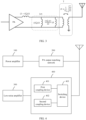
- FIG. 4 is a diagram of a radio frequency switch circuit according to an embodiment of this application.
- the radio frequency switch circuit provided in this embodiment includes: a power amplifier PA output matching network 200 and a low noise amplifier LNA input matching network 400.
- An output end of the PA output matching network 200 is configured to connect to an antenna, and an input end of the PA output matching network 200 is configured to connect to a power amplifier 100.
- the LNA input matching network 400 includes: a first coupling device 401, a second coupling device 402, and a switching device 403, where the first coupling device 401 and the second coupling device 402 are coupled to each other. It should be understood that the first coupling device 401 and the second coupling device 402 are mainly magnetically coupled.
- a first end of the first coupling device 401 is configured to connect to the antenna, a second end of the first coupling device 401 is connected to a first end of the switching device 403, the second end of the first coupling device 401 is connected to a first end of a low noise amplifier 300, a second end of the switching device 403 is connected to a first end of the second coupling device 402, a second end of the second coupling device 402 is grounded, and a third end of the second coupling device 402 is connected to a second end of the low noise amplifier 300.
- the switching device 403 is turned on, so that the first coupling device 401 and the second coupling device 402 are connected in series; and during signal reception, the switching device 403 is turned off.
- the first coupling device 401 and the second coupling device 403 are not specifically limited in this embodiment of this application.
- the first coupling device 401 includes a first inductor
- the second coupling device 402 includes a second inductor
- the first end of the first coupling device 401 and the first end of the second coupling device are dotted terminals
- the first inductor and the second inductor are magnetically coupled to each other.
- the first coupling device 401 and the second coupling device 402 may be implemented by using a coupled transmission line.
- a function of the coupled transmission line is similar to that of an inductor.
- the switching device during signal transmission, the switching device is turned on.
- the first coupling device and the second coupling device are connected in series, and therefore, overall impedance after the serial connection increases. Therefore, an equivalent coupling inductance of a transformer may be increased, and thus an equivalent coupling coefficient of the transformer is increased, so that an output power and efficiency of the PA can be improved.
- strength of a signal transferred from the PA to the antenna is greater, thereby improving work efficiency.
- a radio frequency signal output by the PA needs to pass through the PA output matching network to reach the antenna, but a part of the signal is transmitted to ground, that is, lost, by passing through the series-connected first coupling device and the second coupling device.
- the first coupling device and the second coupling device are connected in series, so that a signal loss path has high impedance, resulting in fewer signals lost from the series-connected first coupling device and the second coupling device to the ground.
- FIG. 5 is a diagram of still another radio frequency switch circuit according to an embodiment of this application.
- a coupling device provided in this embodiment of this application is implemented by an inductor.
- a first coupling device is a first inductor L3
- a second coupling device is a second inductor L4, where a first end of the first inductor L3 and a first end of the second inductor L4 are dotted terminals, and the first inductor L3 and the second inductor L4 is magnetically coupled.
- a switching device is SW 1. It can be learned from FIG. 5 that, a first end of the switching device SW 1 is connected to the first inductor L3, a second end of the switching device SW 1 is connected to a first end of the second inductor L4, a second end of the second inductor L4 is grounded, a third end of the second inductor L4 is connected to a second end of a low noise amplifier LNA, and a second end of the first inductor L3 is connected to a first end of the low noise amplifier LNA.
- the second inductor L4 is a three-terminal device, that is, the second inductor L4 includes a center tap, that is, the center tap of the second inductor L4 is connected to a source of the low noise amplifier LNA, to form a source negative feedback circuit.
- a PA output matching network 200 includes a transformer
- An output end of a power amplifier PA is connected to a first winding L1 of the transformer, a first end of a second winding L2 of the transformer is connected to an antenna, and a second end of the second winding L2 is grounded.
- the PA output matching network 200 shown in FIG. 5 includes a transformer, where the transformer may also be replaced by another component, for example, a transmission-line balun or a coupled transmission line.
- the switching device SW 1 During signal transmission, that is, when the power amplifier PA transmits a signal to the antenna, the switching device SW 1 is turned on, so that the first inductor L3 and the second inductor L4 are connected in series; and during signal reception, the switching device SW 1 is turned off.
- FIG. 6 is a diagram of a specific circuit corresponding to FIG. 5 .
- FIG. 6 an example in which the low noise amplifier includes a switching transistor NM 1 is used, and the PA output matching network 200 and the LNA input matching network 400 are improved.
- the LNA input matching network 400 further includes a direct-current blocking capacitor Cin.
- the second end of the first inductor L3 is connected to a first end of the switching transistor NM 1 through the direct-current blocking capacitor Cin, a third end of the switching transistor NM 1 is connected to the third end of the second inductor L4, and a second end of the switching transistor NM 1 serves as a signal output end (out) of the LNA.
- the PA output matching network further includes: a first matching capacitor C1 and a second matching capacitor C2.
- the first matching capacitor C1 is connected in parallel to two ends of the first winding L1
- the second matching capacitor C2 is connected in parallel to two ends of the second winding L2, that is, the PA output matching network is an LC matching network.
- the switching device SW 1 is an NMOS transistor NM 2
- the switching transistor NM 1 is also an NMOS transistor is used for description.
- the first inductor L3 and the second inductor L4 at least partially overlap in space, so that the two inductors may occupy an area of only one inductor.
- FIG. 7 is a diagram of an equivalent circuit of signal transmission corresponding to FIG. 5 .
- FIG. 7 shows a circuit during signal transmission, that is, a circuit connection relationship when the switching device SW 1 is turned on during signal transmission.
- SW 1 is turned on, and the first inductor L3 and the second inductor L4 and the L3m and the L4m are connected in series and then grounded.
- SW 1 is turned off, and a current flowing through the low noise amplifier is grounded through L4.
- FIG. 8 is a diagram of an equivalent circuit of signal reception corresponding to FIG. 5 .
- the switching device SW 1 is turned off, where Cpa is a parasitic capacitor when the power amplifier does not work, and a represents a tap position at which a source of the switching transistor NM 1 is connected to the second inductor L4.
- L3m1 and L4m1 respectively represent the coupled inductances generated by coupling of the first inductor L3 and the second inductor L4.
- a position of the tap can be adjusted to change a value of an inductance a(L4+L4m1) between the source of NM 1 and the ground, so that the source negative feedback inductance a(L4+L4m1) can also be adjusted to an optimal value, to meet a requirement of the low noise amplifier LNA input matching network.
- a manner of adjusting a position of a is not specifically limited in this embodiment of this application.
- a plurality of switches may be disposed, and a specific position of a is changed by controlling different states of the switches.
- a semiconductor process may be used for implementation.
- the inductor is implemented by using a metal wire on a circuit board, and the position of a may be changed by interrupting the metal wire by using a laser.
- the position of a may be selected based on a specific application scenario, so that an inductance value is adjusted to an optimal value. In this way, the inductance is adjusted more flexibly, facilitating a design of a circuit layout.
- the source of the low noise amplifier LNA is grounded through the inductor, so that a real part of an input impedance at a gate end of a transistor in the low noise amplifier LNA can be increased.
- a complex input matching network needs to be designed. Further, the relatively small input impedance reduces a bandwidth, and the complex input matching network increases an insertion loss and a noise.
- the source of the low noise amplifier LNA is grounded through the inductor, to form a source negative feedback, so that the real part of the input impedance at the gate end of the transistor in the low noise amplifier LNA can be increased, thereby increasing the bandwidth, and reducing the insertion loss and the noise.
- the following analyzes, with reference to formulas, how the radio frequency switch circuit provided in this embodiment of this application can increase an output power of the PA.
- L3+L3m needs to be an optimal value of an LNA input matching inductance shown in FIG. 2 .
- L m0 is an equivalent coupling inductance of the transformer shown in FIG. 2
- L m1 is an equivalent coupling inductance of the transformer shown in FIG. 5 . It can be learned by comparing the foregoing two formulas that, the equivalent coupling inductance of the transformer shown in FIG. 5 is greater than the equivalent coupling inductance of the transformer shown in FIG. 2 . Therefore, the radio frequency switch circuit provided in this embodiment of this application improves an equivalent coupling coefficient of the transformer. When the equivalent coupling coefficient of the transformer is larger, more energy is transferred by the transformer from the first winding to the second winding, that is, energy transmission efficiency is higher. Therefore, the radio frequency switch circuit provided in this embodiment of this application can improve the output power and efficiency of the PA, and can further increase a bandwidth of a wireless communication signal of an electronic device, and improve transmission efficiency.
- Q eq0 is an equivalent quality factor of FIG. 2
- Q eq1 is an equivalent quality factor of FIG. 5 .
- the formula indicates that the equivalent quality factor of FIG. 5 is greater than that of FIG. 2 . Therefore, the equivalent quality factor of the PA output matching network is improved, so that the output power and efficiency of the PA are improved.
- the radio frequency switch circuit provided in this embodiment of this application further includes a controller.
- the controller is configured to: during signal transmission, send a drive signal to a control end of the switching device to control the switching device to be turned on, so that the first coupling device and the second coupling device are connected in series; and during signal reception, send a drive signal to the control end of the switching device to control the switching device to be turned off.
- the controller may be a controller of the radio frequency switch circuit, or may be a controller of an entire wireless transceiver system.
- the controller may be a microprocessor, a single-chip microcomputer, or the like.
- the controller needs to send a driving pulse signal to a gate of the switching transistor or the switching device.
- the foregoing embodiments describe a coupling device in the radio frequency switch circuit with an example in which the coupling device is an inductor.
- FIG. 9 is a diagram of yet another radio frequency switch circuit according to an embodiment of this application.
- a coupling device in the radio frequency switch circuit provided in this embodiment is implemented by a coupled transmission line.
- the coupled transmission line includes a first coupled transmission line A and a second coupled transmission line B.
- a first end of the first coupled transmission line A is connected to an antenna, and a second end of the first coupled transmission line A is connected to a first end of a low noise amplifier NM 1 through a direct-current blocking capacitor Cin.
- the second coupled transmission line B similar to a second inductor, is also a three-terminal device.
- a first end of the second coupled transmission line B is connected to a second end of a switching device SW 1 (NM 2), a second end of the second coupled transmission line B is grounded, and a third end of the second coupled transmission line B is connected to a source of the switching transistor NM 1 to form a source negative feedback circuit.
- the coupled transmission line has the same function as an inductor, only with a different representation form.
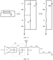
- FIG. 10 is a diagram of an equivalent model of coupled transmission lines according to an embodiment of this application.
- FIG. 10 shows the equivalent model of the coupled transmission lines, in which inductors and capacitors are included. The following describes the equivalent circuit diagram of the equivalent model shown in FIG. 10 with reference to the accompanying drawing.
- FIG. 11 is a diagram of an equivalent circuit corresponding to FIG. 10 .
- the coupled transmission lines may be equivalent to two inductors L3 and L4, which are similar to a first inductor and a second inductor described in the foregoing embodiment; L3m and L4m are coupled inductors between the two inductors L3 and L4, and are equivalent to three capacitors, which are C3, C4, and C5, respectively; and a circuit on a left side in FIG. 11 is equivalent to a circuit on a right side in FIG. 11 , that is, the three capacitors C3, C4, and C5 are equivalent to one capacitor C345.
- An equivalent radio frequency switch circuit of the coupled transmission lines may be obtained according to FIG. 11 .
- FIG. 12 is a diagram of an equivalent circuit of signal transmission corresponding to FIG. 9 .
- FIG. 12 is a diagram of an equivalent circuit diagram of signal transmission, that is, a PA transmits a radio frequency signal to an antenna.
- the switching device SW 1 is turned on, the first coupled transmission line and the second coupled transmission line are connected in series, that is, equivalent inductors and mutual inductors are all connected in series, and L3, L3m, L4m, and L4 are all connected in series, and are grounded after being connected in series.
- a first end of the equivalent capacitor C345 is connected to the antenna, and a second end of the equivalent capacitor C345 is grounded.
- C 345 C 5 + L 3 + L 3 m 2 C 3 + L 4 + L 4 m 2 C 4 L 3 + L 3 m + L 4 + L 4 m ⁇ ⁇ 2 L 3 + L 3 m L 4 + L 4 m C 3 C 4 L 3 + L 3 m + L 4 + L 4 m ⁇ ⁇ 2 L 3 + L 3 m L 4 + L 4 m C 3 + C 4
- ⁇ is an operating frequency of the circuit.
- C345 and C2 may be combined into one capacitor.
- an impact of series-connected inductors in an LNA input matching network on a PA output matching network is the same as that in the embodiment corresponding to FIG. 7 .
- the coupling device in the radio frequency switch circuit provided in this embodiment of this application is implemented by using the coupled transmission line, an effect is the same as that can be achieved by the embodiment corresponding to FIG. 7 .
- impedance of the low noise amplifier LNA input matching network can be increased, so that a radio frequency signal is prevented from leaking to ground through the low noise amplifier LNA input matching network. This increases a transmit power of the power amplifier PA, and improves transmission efficiency of the radio frequency signal of the radio frequency switch circuit.
- an embodiment of this application further provides a wireless transceiver system.
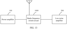
- FIG. 13 is a diagram of a wireless transceiver system according to an embodiment of this application.
- the wireless transceiver system provided in this embodiment of this application includes a radio frequency switch circuit 1000 described in the foregoing embodiments, and further includes a power amplifier 100 and a low noise amplifier 200.
- the power amplifier 100 is connected to an antenna through a power amplifier output matching network in the radio frequency switch circuit.
- the power amplifier 100 is configured to send a wireless signal to the antenna through the power amplifier output matching network, where the antenna is configured to transmit the wireless signal.
- the low noise amplifier 200 is connected to the antenna through a low noise amplifier input matching network in the radio frequency switch circuit.
- the low noise amplifier 200 is configured to receive a wireless signal from the antenna through the low noise amplifier input matching network.
- the other end of the power amplifier 100 may be connected to a frequency mixer or a phase shifter, and is configured to generate a radio frequency signal.
- the power amplifier 100 sends the radio frequency signal to the antenna through the radio frequency switch circuit 1000, and the antenna transmits the radio frequency signal.
- the radio frequency switch circuit included in the wireless transceiver system provided in this embodiment of this application can improve an output power and efficiency of a power amplifier, an overall transmit power of the wireless transceiver system is increased, and signal transmission efficiency is also improved.
- an embodiment of this application further provides an electronic device. The following describes in detail with reference to the accompanying drawing.
- FIG. 14 is a diagram of an electronic device according to an embodiment of this application.
- An electronic device 3000 provided in this embodiment of this application includes a wireless transceiver system 2000, and further includes an antenna.
- the wireless transceiver system 2000 is connected to the antenna.
- the antenna is configured to transmit a wireless signal of the wireless transceiver system 2000, and is configured to send a received wireless signal to the wireless transceiver system 2000.
- the wireless transceiver system included in the electronic device provided in this embodiment of this application includes a radio frequency switch circuit. Therefore, during signal transmission, a switching device is turned on. In this case, a first coupling device and a second coupling device are connected in series, and therefore, overall impedance after the serial connection increases. Therefore, an equivalent coupling inductance of a transformer may be increased, and thus an equivalent coupling coefficient of the transformer is increased, so that an output power and efficiency of a PA can be improved. In other words, during signal transmission, strength of a signal transferred from the PA to the antenna is greater, thereby improving work efficiency.
- a radio frequency signal output by the PA needs to pass through a PA output matching network to reach the antenna, but a part of the signal is transmitted to ground, that is, lost, by passing through the series-connected first coupling device and the second coupling device.
- the first coupling device and the second coupling device are connected in series, so that a signal loss path has high impedance, resulting in fewer signals lost from the series-connected first coupling device and the second coupling device to the ground. Therefore, transmission efficiency of a wireless signal is improved, so that a communication bandwidth of the electronic device can be increased, and communication efficiency can be improved.
- At least one (item) refers to one or more and "a plurality of” refers to two or more.
- the term “and/or” is used for describing an association relationship between associated objects, and represents that three relationships may exist.
- a and/or B may represent the following three cases: Only A exists, only B exists, and both A and B exist, where A and B may be singular or plural.
- the character “/” generally indicates an "or” relationship between the associated objects.
- At least one of the following items (pieces) or a similar expression thereof means any combination of these items, including any combination of singular items (pieces) or plural items (pieces).
- At least one of a, b, or c may indicate a, b, c, a and b, a and c, b and c, or a, b, and c, where a, b, and c may be singular or plural.
Landscapes
- Engineering & Computer Science (AREA)
- Computer Networks & Wireless Communication (AREA)
- Signal Processing (AREA)
- Power Engineering (AREA)
- Microelectronics & Electronic Packaging (AREA)
- Transmitters (AREA)
- Transceivers (AREA)
Applications Claiming Priority (2)
| Application Number | Priority Date | Filing Date | Title |
|---|---|---|---|
| CN202210603028.9A CN117200711A (zh) | 2022-05-30 | 2022-05-30 | 一种射频开关电路、无线收发系统及电子设备 |
| PCT/CN2023/095754 WO2023231832A1 (zh) | 2022-05-30 | 2023-05-23 | 一种射频开关电路、无线收发系统及电子设备 |
Publications (2)
| Publication Number | Publication Date |
|---|---|
| EP4513752A1 true EP4513752A1 (de) | 2025-02-26 |
| EP4513752A4 EP4513752A4 (de) | 2025-08-13 |
Family
ID=88996554
Family Applications (1)
| Application Number | Title | Priority Date | Filing Date |
|---|---|---|---|
| EP23815016.3A Pending EP4513752A4 (de) | 2022-05-30 | 2023-05-23 | Funkfrequenzschaltkreis, drahtloses sende-/empfangssystem und elektronische vorrichtung |
Country Status (4)
| Country | Link |
|---|---|
| US (1) | US20250096745A1 (de) |
| EP (1) | EP4513752A4 (de) |
| CN (1) | CN117200711A (de) |
| WO (1) | WO2023231832A1 (de) |
Families Citing this family (4)
| Publication number | Priority date | Publication date | Assignee | Title |
|---|---|---|---|---|
| WO2025140091A1 (zh) * | 2023-12-29 | 2025-07-03 | 德氪微电子(深圳)有限公司 | 一种高频毫米波数字隔离器 |
| US20250240039A1 (en) * | 2024-01-23 | 2025-07-24 | Qualcomm Incorporated | Concurrent matching receiver with improved noise figure |
| CN118199665B (zh) * | 2024-03-25 | 2025-12-16 | 华南理工大学 | 收发匹配网络和射频前端电路、芯片 |
| CN118826762B (zh) * | 2024-07-10 | 2025-01-28 | 优镓科技(苏州)有限公司 | 基于耦合线的射频前端 |
Family Cites Families (9)
| Publication number | Priority date | Publication date | Assignee | Title |
|---|---|---|---|---|
| US8229367B2 (en) * | 2009-04-14 | 2012-07-24 | Qualcomm, Incorporated | Low noise amplifier with combined input matching, balun, and transmit/receive switch |
| US8626084B2 (en) * | 2010-05-13 | 2014-01-07 | Qualcomm, Incorporated | Area efficient concurrent matching transceiver |
| US20140015614A1 (en) * | 2012-07-10 | 2014-01-16 | Infineon Technologies Ag | System and Method for a Low Noise Amplifier |
| US9825597B2 (en) * | 2015-12-30 | 2017-11-21 | Skyworks Solutions, Inc. | Impedance transformation circuit for amplifier |
| US10574286B2 (en) * | 2017-09-01 | 2020-02-25 | Qualcomm Incorporated | High selectivity TDD RF front end |
| CN108063600B (zh) * | 2018-01-03 | 2021-07-06 | 上海华虹宏力半导体制造有限公司 | 一种低噪声放大器及射频前端集成电路 |
| JP2020198567A (ja) * | 2019-06-04 | 2020-12-10 | 旭化成エレクトロニクス株式会社 | 低ノイズアンプ回路 |
| CN110932747B (zh) * | 2019-12-02 | 2020-08-21 | 翱捷智能科技(上海)有限公司 | 集成高性能射频收发开关 |
| CN113517869A (zh) * | 2021-06-24 | 2021-10-19 | 成都爱旗科技有限公司 | 一种低噪声放大器、信号收发设备及信号收发方法 |
-
2022
- 2022-05-30 CN CN202210603028.9A patent/CN117200711A/zh active Pending
-
2023
- 2023-05-23 WO PCT/CN2023/095754 patent/WO2023231832A1/zh not_active Ceased
- 2023-05-23 EP EP23815016.3A patent/EP4513752A4/de active Pending
-
2024
- 2024-11-28 US US18/963,547 patent/US20250096745A1/en active Pending
Also Published As
| Publication number | Publication date |
|---|---|
| EP4513752A4 (de) | 2025-08-13 |
| WO2023231832A1 (zh) | 2023-12-07 |
| US20250096745A1 (en) | 2025-03-20 |
| CN117200711A (zh) | 2023-12-08 |
Similar Documents
| Publication | Publication Date | Title |
|---|---|---|
| EP4513752A1 (de) | Funkfrequenzschaltkreis, drahtloses sende-/empfangssystem und elektronische vorrichtung | |
| CN102868419B (zh) | 收发器及集成电路 | |
| JP6163350B2 (ja) | 伝送回路、及び、信号送受信回路 | |
| EP3785374B1 (de) | Sende- und empfangsschalter und breitbandleistungsverstärkeranpassungssystem für mehrbandmillimeterwellen-5g-kommunikation | |
| US7209727B2 (en) | Integrated circuit radio front-end architecture and applications thereof | |
| US20040192230A1 (en) | Duplexer structure for coupling a transmitter and a receiver to a common antenna | |
| US20100019858A1 (en) | N:m transformer and impedance matching | |
| EP3349354B1 (de) | Anpassungsnetzwerk für klasse-f-leistungsverstärker | |
| US20220173700A1 (en) | Power amplifier with series transformer combiners and harmonic tuning | |
| CN111342860A (zh) | 一种射频收发开关集成电路及收发方法 | |
| CN219980795U (zh) | 一种巴伦结构电路及信号转换装置 | |
| WO2016202370A1 (en) | A radio frequency transformer for transforming an input radio frequency signal into an output radio frequency signal | |
| US9531339B2 (en) | Integrated circuit for transmitting and receiving an RF signal | |
| US20230022015A1 (en) | Compact Antenna Impedance Tuner | |
| US12095489B2 (en) | High-frequency circuit and communication device | |
| CN218301375U (zh) | 功率检测装置及射频前端模组 | |
| CN115211042B (zh) | 一种收发机装置、无线通信装置及芯片组 | |
| CN102130703B (zh) | 信号传收电路 | |
| US12609663B2 (en) | Radio-frequency module and communication device | |
| CN222602412U (zh) | 一种变压器输出匹配电路、射频前端模组和无线通信模组 | |
| US20250080077A1 (en) | Parallel-type tx/rx concurrent impedance matching utilizing rx mutual inductance matching | |
| US7812780B2 (en) | Antenna architecture and LC coupler | |
| CN112994728A (zh) | 一种差动收发机的共埠架构及其差动收发机 | |
| KR20250028967A (ko) | 스위치 가능 코일 및 이를 포함하는 송신 회로 | |
| CN117118361A (zh) | 一种倍频电路、倍频器及射频系统 |
Legal Events
| Date | Code | Title | Description |
|---|---|---|---|
| STAA | Information on the status of an ep patent application or granted ep patent |
Free format text: STATUS: THE INTERNATIONAL PUBLICATION HAS BEEN MADE |
|
| PUAI | Public reference made under article 153(3) epc to a published international application that has entered the european phase |
Free format text: ORIGINAL CODE: 0009012 |
|
| STAA | Information on the status of an ep patent application or granted ep patent |
Free format text: STATUS: REQUEST FOR EXAMINATION WAS MADE |
|
| 17P | Request for examination filed |
Effective date: 20241121 |
|
| AK | Designated contracting states |
Kind code of ref document: A1 Designated state(s): AL AT BE BG CH CY CZ DE DK EE ES FI FR GB GR HR HU IE IS IT LI LT LU LV MC ME MK MT NL NO PL PT RO RS SE SI SK SM TR |
|
| REG | Reference to a national code |
Ref country code: DE Ref legal event code: R079 Free format text: PREVIOUS MAIN CLASS: H03F0001260000 Ipc: H04B0001440000 |
|
| A4 | Supplementary search report drawn up and despatched |
Effective date: 20250714 |
|
| RIC1 | Information provided on ipc code assigned before grant |
Ipc: H04B 1/44 20060101AFI20250708BHEP Ipc: H04B 1/04 20060101ALI20250708BHEP Ipc: H04B 1/18 20060101ALI20250708BHEP Ipc: H03F 1/34 20060101ALI20250708BHEP Ipc: H03F 1/56 20060101ALI20250708BHEP Ipc: H03F 3/195 20060101ALI20250708BHEP Ipc: H03F 3/24 20060101ALI20250708BHEP |
|
| DAV | Request for validation of the european patent (deleted) | ||
| DAX | Request for extension of the european patent (deleted) | ||
| GRAP | Despatch of communication of intention to grant a patent |
Free format text: ORIGINAL CODE: EPIDOSNIGR1 |
|
| STAA | Information on the status of an ep patent application or granted ep patent |
Free format text: STATUS: GRANT OF PATENT IS INTENDED |
|
| INTG | Intention to grant announced |
Effective date: 20260126 |