EP4501893A1 - Ceramic structure - Google Patents
Ceramic structure Download PDFInfo
- Publication number
- EP4501893A1 EP4501893A1 EP23780493.5A EP23780493A EP4501893A1 EP 4501893 A1 EP4501893 A1 EP 4501893A1 EP 23780493 A EP23780493 A EP 23780493A EP 4501893 A1 EP4501893 A1 EP 4501893A1
- Authority
- EP
- European Patent Office
- Prior art keywords
- layer
- base
- ceramic
- ave
- ceramic structure
- Prior art date
- Legal status (The legal status is an assumption and is not a legal conclusion. Google has not performed a legal analysis and makes no representation as to the accuracy of the status listed.)
- Pending
Links
Images



Classifications
-
- C—CHEMISTRY; METALLURGY
- C04—CEMENTS; CONCRETE; ARTIFICIAL STONE; CERAMICS; REFRACTORIES
- C04B—LIME, MAGNESIA; SLAG; CEMENTS; COMPOSITIONS THEREOF, e.g. MORTARS, CONCRETE OR LIKE BUILDING MATERIALS; ARTIFICIAL STONE; CERAMICS; REFRACTORIES; TREATMENT OF NATURAL STONE
- C04B41/00—After-treatment of mortars, concrete, artificial stone or ceramics; Treatment of natural stone
- C04B41/009—After-treatment of mortars, concrete, artificial stone or ceramics; Treatment of natural stone characterised by the material treated
-
- C—CHEMISTRY; METALLURGY
- C04—CEMENTS; CONCRETE; ARTIFICIAL STONE; CERAMICS; REFRACTORIES
- C04B—LIME, MAGNESIA; SLAG; CEMENTS; COMPOSITIONS THEREOF, e.g. MORTARS, CONCRETE OR LIKE BUILDING MATERIALS; ARTIFICIAL STONE; CERAMICS; REFRACTORIES; TREATMENT OF NATURAL STONE
- C04B35/00—Shaped ceramic products characterised by their composition; Ceramics compositions; Processing powders of inorganic compounds preparatory to the manufacturing of ceramic products
- C04B35/01—Shaped ceramic products characterised by their composition; Ceramics compositions; Processing powders of inorganic compounds preparatory to the manufacturing of ceramic products based on oxide ceramics
- C04B35/10—Shaped ceramic products characterised by their composition; Ceramics compositions; Processing powders of inorganic compounds preparatory to the manufacturing of ceramic products based on oxide ceramics based on aluminium oxide
-
- C—CHEMISTRY; METALLURGY
- C04—CEMENTS; CONCRETE; ARTIFICIAL STONE; CERAMICS; REFRACTORIES
- C04B—LIME, MAGNESIA; SLAG; CEMENTS; COMPOSITIONS THEREOF, e.g. MORTARS, CONCRETE OR LIKE BUILDING MATERIALS; ARTIFICIAL STONE; CERAMICS; REFRACTORIES; TREATMENT OF NATURAL STONE
- C04B35/00—Shaped ceramic products characterised by their composition; Ceramics compositions; Processing powders of inorganic compounds preparatory to the manufacturing of ceramic products
- C04B35/01—Shaped ceramic products characterised by their composition; Ceramics compositions; Processing powders of inorganic compounds preparatory to the manufacturing of ceramic products based on oxide ceramics
- C04B35/10—Shaped ceramic products characterised by their composition; Ceramics compositions; Processing powders of inorganic compounds preparatory to the manufacturing of ceramic products based on oxide ceramics based on aluminium oxide
- C04B35/111—Fine ceramics
- C04B35/117—Composites
-
- C—CHEMISTRY; METALLURGY
- C04—CEMENTS; CONCRETE; ARTIFICIAL STONE; CERAMICS; REFRACTORIES
- C04B—LIME, MAGNESIA; SLAG; CEMENTS; COMPOSITIONS THEREOF, e.g. MORTARS, CONCRETE OR LIKE BUILDING MATERIALS; ARTIFICIAL STONE; CERAMICS; REFRACTORIES; TREATMENT OF NATURAL STONE
- C04B41/00—After-treatment of mortars, concrete, artificial stone or ceramics; Treatment of natural stone
- C04B41/45—Coating or impregnating, e.g. injection in masonry, partial coating of green or fired ceramics, organic coating compositions for adhering together two concrete elements
- C04B41/50—Coating or impregnating, e.g. injection in masonry, partial coating of green or fired ceramics, organic coating compositions for adhering together two concrete elements with inorganic materials
- C04B41/51—Metallising, e.g. infiltration of sintered ceramic preforms with molten metal
- C04B41/5133—Metallising, e.g. infiltration of sintered ceramic preforms with molten metal with a composition mainly composed of one or more of the refractory metals
-
- C—CHEMISTRY; METALLURGY
- C04—CEMENTS; CONCRETE; ARTIFICIAL STONE; CERAMICS; REFRACTORIES
- C04B—LIME, MAGNESIA; SLAG; CEMENTS; COMPOSITIONS THEREOF, e.g. MORTARS, CONCRETE OR LIKE BUILDING MATERIALS; ARTIFICIAL STONE; CERAMICS; REFRACTORIES; TREATMENT OF NATURAL STONE
- C04B41/00—After-treatment of mortars, concrete, artificial stone or ceramics; Treatment of natural stone
- C04B41/80—After-treatment of mortars, concrete, artificial stone or ceramics; Treatment of natural stone of only ceramics
- C04B41/81—Coating or impregnation
- C04B41/85—Coating or impregnation with inorganic materials
- C04B41/88—Metals
-
- C—CHEMISTRY; METALLURGY
- C04—CEMENTS; CONCRETE; ARTIFICIAL STONE; CERAMICS; REFRACTORIES
- C04B—LIME, MAGNESIA; SLAG; CEMENTS; COMPOSITIONS THEREOF, e.g. MORTARS, CONCRETE OR LIKE BUILDING MATERIALS; ARTIFICIAL STONE; CERAMICS; REFRACTORIES; TREATMENT OF NATURAL STONE
- C04B2235/00—Aspects relating to ceramic starting mixtures or sintered ceramic products
- C04B2235/02—Composition of constituents of the starting material or of secondary phases of the final product
- C04B2235/30—Constituents and secondary phases not being of a fibrous nature
- C04B2235/32—Metal oxides, mixed metal oxides, or oxide-forming salts thereof, e.g. carbonates, nitrates, (oxy)hydroxides, chlorides
- C04B2235/3205—Alkaline earth oxides or oxide forming salts thereof, e.g. beryllium oxide
- C04B2235/3206—Magnesium oxides or oxide-forming salts thereof
-
- C—CHEMISTRY; METALLURGY
- C04—CEMENTS; CONCRETE; ARTIFICIAL STONE; CERAMICS; REFRACTORIES
- C04B—LIME, MAGNESIA; SLAG; CEMENTS; COMPOSITIONS THEREOF, e.g. MORTARS, CONCRETE OR LIKE BUILDING MATERIALS; ARTIFICIAL STONE; CERAMICS; REFRACTORIES; TREATMENT OF NATURAL STONE
- C04B2235/00—Aspects relating to ceramic starting mixtures or sintered ceramic products
- C04B2235/02—Composition of constituents of the starting material or of secondary phases of the final product
- C04B2235/30—Constituents and secondary phases not being of a fibrous nature
- C04B2235/32—Metal oxides, mixed metal oxides, or oxide-forming salts thereof, e.g. carbonates, nitrates, (oxy)hydroxides, chlorides
- C04B2235/3205—Alkaline earth oxides or oxide forming salts thereof, e.g. beryllium oxide
- C04B2235/3208—Calcium oxide or oxide-forming salts thereof, e.g. lime
-
- C—CHEMISTRY; METALLURGY
- C04—CEMENTS; CONCRETE; ARTIFICIAL STONE; CERAMICS; REFRACTORIES
- C04B—LIME, MAGNESIA; SLAG; CEMENTS; COMPOSITIONS THEREOF, e.g. MORTARS, CONCRETE OR LIKE BUILDING MATERIALS; ARTIFICIAL STONE; CERAMICS; REFRACTORIES; TREATMENT OF NATURAL STONE
- C04B2235/00—Aspects relating to ceramic starting mixtures or sintered ceramic products
- C04B2235/02—Composition of constituents of the starting material or of secondary phases of the final product
- C04B2235/30—Constituents and secondary phases not being of a fibrous nature
- C04B2235/34—Non-metal oxides, non-metal mixed oxides, or salts thereof that form the non-metal oxides upon heating, e.g. carbonates, nitrates, (oxy)hydroxides, chlorides
- C04B2235/3418—Silicon oxide, silicic acids or oxide forming salts thereof, e.g. silica sol, fused silica, silica fume, cristobalite, quartz or flint
-
- C—CHEMISTRY; METALLURGY
- C04—CEMENTS; CONCRETE; ARTIFICIAL STONE; CERAMICS; REFRACTORIES
- C04B—LIME, MAGNESIA; SLAG; CEMENTS; COMPOSITIONS THEREOF, e.g. MORTARS, CONCRETE OR LIKE BUILDING MATERIALS; ARTIFICIAL STONE; CERAMICS; REFRACTORIES; TREATMENT OF NATURAL STONE
- C04B2235/00—Aspects relating to ceramic starting mixtures or sintered ceramic products
- C04B2235/65—Aspects relating to heat treatments of ceramic bodies such as green ceramics or pre-sintered ceramics, e.g. burning, sintering or melting processes
- C04B2235/652—Reduction treatment
-
- C—CHEMISTRY; METALLURGY
- C04—CEMENTS; CONCRETE; ARTIFICIAL STONE; CERAMICS; REFRACTORIES
- C04B—LIME, MAGNESIA; SLAG; CEMENTS; COMPOSITIONS THEREOF, e.g. MORTARS, CONCRETE OR LIKE BUILDING MATERIALS; ARTIFICIAL STONE; CERAMICS; REFRACTORIES; TREATMENT OF NATURAL STONE
- C04B2235/00—Aspects relating to ceramic starting mixtures or sintered ceramic products
- C04B2235/65—Aspects relating to heat treatments of ceramic bodies such as green ceramics or pre-sintered ceramics, e.g. burning, sintering or melting processes
- C04B2235/658—Atmosphere during thermal treatment
- C04B2235/6582—Hydrogen containing atmosphere
-
- C—CHEMISTRY; METALLURGY
- C04—CEMENTS; CONCRETE; ARTIFICIAL STONE; CERAMICS; REFRACTORIES
- C04B—LIME, MAGNESIA; SLAG; CEMENTS; COMPOSITIONS THEREOF, e.g. MORTARS, CONCRETE OR LIKE BUILDING MATERIALS; ARTIFICIAL STONE; CERAMICS; REFRACTORIES; TREATMENT OF NATURAL STONE
- C04B2235/00—Aspects relating to ceramic starting mixtures or sintered ceramic products
- C04B2235/70—Aspects relating to sintered or melt-casted ceramic products
- C04B2235/74—Physical characteristics
- C04B2235/78—Grain sizes and shapes, product microstructures, e.g. acicular grains, equiaxed grains, platelet-structures
- C04B2235/786—Micrometer sized grains, i.e. from 1 to 100 micron
-
- C—CHEMISTRY; METALLURGY
- C04—CEMENTS; CONCRETE; ARTIFICIAL STONE; CERAMICS; REFRACTORIES
- C04B—LIME, MAGNESIA; SLAG; CEMENTS; COMPOSITIONS THEREOF, e.g. MORTARS, CONCRETE OR LIKE BUILDING MATERIALS; ARTIFICIAL STONE; CERAMICS; REFRACTORIES; TREATMENT OF NATURAL STONE
- C04B2237/00—Aspects relating to ceramic laminates or to joining of ceramic articles with other articles by heating
- C04B2237/02—Aspects relating to interlayers, e.g. used to join ceramic articles with other articles by heating
- C04B2237/04—Ceramic interlayers
- C04B2237/06—Oxidic interlayers
- C04B2237/064—Oxidic interlayers based on alumina or aluminates
-
- C—CHEMISTRY; METALLURGY
- C04—CEMENTS; CONCRETE; ARTIFICIAL STONE; CERAMICS; REFRACTORIES
- C04B—LIME, MAGNESIA; SLAG; CEMENTS; COMPOSITIONS THEREOF, e.g. MORTARS, CONCRETE OR LIKE BUILDING MATERIALS; ARTIFICIAL STONE; CERAMICS; REFRACTORIES; TREATMENT OF NATURAL STONE
- C04B2237/00—Aspects relating to ceramic laminates or to joining of ceramic articles with other articles by heating
- C04B2237/30—Composition of layers of ceramic laminates or of ceramic or metallic articles to be joined by heating, e.g. Si substrates
- C04B2237/32—Ceramic
- C04B2237/34—Oxidic
- C04B2237/343—Alumina or aluminates
-
- C—CHEMISTRY; METALLURGY
- C04—CEMENTS; CONCRETE; ARTIFICIAL STONE; CERAMICS; REFRACTORIES
- C04B—LIME, MAGNESIA; SLAG; CEMENTS; COMPOSITIONS THEREOF, e.g. MORTARS, CONCRETE OR LIKE BUILDING MATERIALS; ARTIFICIAL STONE; CERAMICS; REFRACTORIES; TREATMENT OF NATURAL STONE
- C04B2237/00—Aspects relating to ceramic laminates or to joining of ceramic articles with other articles by heating
- C04B2237/30—Composition of layers of ceramic laminates or of ceramic or metallic articles to be joined by heating, e.g. Si substrates
- C04B2237/40—Metallic
- C04B2237/403—Refractory metals
-
- C—CHEMISTRY; METALLURGY
- C04—CEMENTS; CONCRETE; ARTIFICIAL STONE; CERAMICS; REFRACTORIES
- C04B—LIME, MAGNESIA; SLAG; CEMENTS; COMPOSITIONS THEREOF, e.g. MORTARS, CONCRETE OR LIKE BUILDING MATERIALS; ARTIFICIAL STONE; CERAMICS; REFRACTORIES; TREATMENT OF NATURAL STONE
- C04B2237/00—Aspects relating to ceramic laminates or to joining of ceramic articles with other articles by heating
- C04B2237/50—Processing aspects relating to ceramic laminates or to the joining of ceramic articles with other articles by heating
- C04B2237/59—Aspects relating to the structure of the interlayer
Definitions
- Embodiments of the present disclosure relate to a ceramic structure.
- Ceramics are widely used for structures from the perspectives of strength, insulation, heat resistance, and the like.
- a structure in which a metallization layer is provided on a surface of a base made of a ceramic is known. For example, see Patent Document 1.
- Patent Document 1 JP 4348112 B
- a ceramic structure of the present disclosure includes a base, a first layer, and a second layer.
- the base is made of a ceramic.
- the first layer is positioned to be in contact with a surface of the base and is made of a ceramic having a composition different from a composition in the base.
- the second layer is positioned to be in contact with a surface of the first layer and is made of metal.
- D B is a mean grain size of a main crystal in the base
- D 1 to D n are measured values of thicknesses of the first layer measured every 1 ⁇ m
- D AVE is a mean value of D 1 to D n
- the first layer has irregularities where
- Ceramics are widely used for structures from the perspectives of strength, insulation, heat resistance, and the like.
- As the ceramic structure a structure in which a metallization layer is provided on a surface of a base made of a ceramic is known.
- FIG. 1 is a schematic perspective view of a ceramic structure 1 according to an embodiment
- FIG. 2 is an enlarged cross-sectional view illustrating the example of the configuration of the ceramic structure 1 according to the embodiment. Note that FIG. 2 is a cross-sectional view taken along line A-A illustrated in FIG. 1 .
- the ceramic structure 1 includes a base 2, a first layer 3, and a second layer 4.
- the base 2 has, for example, a rectangular parallelepiped shape and has a surface 2a.
- the shape of the base 2 is not limited to the example illustrated in FIG. 2 , and may be any shape such as a plate shape, a frame shape, or a pillar shape.
- the base 2 is a sintered ceramic body.
- the ceramic constituting the base 2 include ceramics containing aluminum oxide (Al 2 O 3 ), silicon carbide (SiC), silicon carbonitride (SiCN), titanium carbide (TiC), and titanium carbonitride (TiCN) as main components.
- main component refers to a component that accounts for 80 mass% or more of a total 100 mass% of the components constituting the ceramic.
- Each of components contained in the ceramic may be identified with an X-ray diffractometer using CuK ⁇ rays, and a content of each component may be determined, for example, with an inductively coupled plasma (ICP) optical emission spectrometer or an X-ray fluorescence analyzer.
- ICP inductively coupled plasma
- the base 2 containing aluminum oxide as the main component exhibits excellent mechanical characteristics while being relatively inexpensive in terms of raw material cost and manufacturing cost as well among ceramics.
- the base 2 containing aluminum oxide as the main component may further contain, for example, oxides of magnesium (Mg), calcium (Ca), and silicon (Si).
- the first layer 3 is positioned to be in contact with the surface 2a of the base 2.
- the first layer 3 is made of a ceramic having a composition different from that in the base 2.
- Constituent elements of the first layer 3 may include, for example, at least one element contained in the base 2 and at least one element contained in the second layer 4.
- the second layer 4 is positioned to be in contact with a surface 3a of the first layer 3.
- the second layer 4 is made of metal and is also referred to as a metallization layer.
- the second layer 4 may be formed from, for example, a metal material such as molybdenum (Mo), manganese (Mn), tungsten (W), copper (Cu), silver (Ag), palladium (Pd), gold (Au), or platinum (Pt), or an alloy of these metal materials.
- the second layer 4 may contain, for example, molybdenum and manganese.
- the second layer 4, which is a metal layer can be formed with good adhesion to the base 2 made of a ceramic.
- the second layer 4 can be formed by, for example, applying a metal paste prepared by kneading powder of the above metal material together with an organic solvent, a binder, and the like to a ceramic green sheet that serves as the base 2, and simultaneously sintering the ceramic green sheet with the metal paste in a reducing atmosphere.
- the first layer 3, which is an intermediate layer, is formed at an interface between the base 2 and the second layer 4.
- FIGs. 1 and 2 illustrates an example in which the second layer 4 is exposed
- the present disclosure is not limited to this example, and another layer such as nickel (Ni) plating may be provided on a surface of the second layer 4.
- Ni nickel
- D B is a mean grain size of a main crystal (not illustrated) in the base 2
- D 1 to D n are measured values of thicknesses of the first layer 3 measured every 1 ⁇ m
- D AVE is a mean value of D 1 to D n .
- n in D n is an integer.
- the main crystal refers to crystals that occupy 50 area% or more in the base.
- the first layer 3 has irregularities where
- the adhesion of the first layer 3 to the base 2 can be enhanced, the adhesion between the base 2 and the second layer 4 can be improved.
- a minimum contact width between the base 2 and the first layer 3 is 1 mm or more, the adhesion is particularly high. From the viewpoint of adhesion, the minimum contact width may be 2 mm or more, and even 3 mm or more.
- the main crystal of the base 2 may be aluminum oxide. That is, the main component of the base 2 may be aluminum oxide.
- the ceramic structure 1 can exhibit excellent mechanical characteristics while being relatively inexpensive in terms of raw material cost and manufacturing cost as well.
- the constituent elements of the first layer 3 may include at least one element contained in the base 2 and at least one element contained in the second layer 4.
- the first layer 3 may contain Mg, Al, Mn, and O.
- the first layer 3, which is the intermediate layer, contains both the elements contained in the base 2 and the second layer 4, thereby the adhesion between the base 2 and the first layer 3 and the adhesion between the first layer 3 and the second layer 4 can be improved.
- the adhesion between the base 2 and the second layer 4 can be further improved.
- the first layer 3 may contain crystals having a spinel crystal structure.
- the base 2 contains Al, Mg, Ca, Si, and O
- the second layer 4 contains Mo and Mn
- the first layer 3 may contain at least either of MgO ⁇ Al 2 O 3 spinel crystals and MnO ⁇ Al 2 O 3 spinel crystals.
- a thermal expansion coefficient of the base 2 containing aluminum oxide as a main component and a thermal expansion coefficient of the first layer 3 containing the spinel crystals described above can be made close to each other. Consequently, according to the embodiment, peeling between the base 2 and the second layer 4 due to thermal cycles can be reduced.
- a thickness t of the base 2 when the second layer 4 is placed on an upper surface thereof may be 2.0 mm or more.
- the ceramic structure 1 having high insulation properties with respect to the second layer 4, which is the metallization layer, can be achieved.
- powders of aluminum oxide which is the main component of the base 2
- powders of silicon oxide (SiO 2 ), magnesium oxide (MgO), and calcium oxide (CaO) as sintering aids were prepared.
- the powders of aluminum oxide and the powders of the sintering aids were mixed so as to be Al 2 O 3 : 90 mass%, SiO 2 : 7 mass%, MgO: 2 mass%, and CaO: 1 mass%, and water and a dispersant were added, and then the mixture is mixed for a predetermined period of time using a ball mill, a bead mill, or the like to obtain a primary slurry.
- an organic binder was added to and mixed with the obtained primary slurry to obtain a secondary slurry. Then, the obtained secondary slurry was spray-dried to obtain granules containing aluminum oxide as a main component.
- the obtained granules were filled into a predetermined molding die and press-molded into a predetermined shape, for example, a rectangular parallelepiped shape, under an appropriately set pressure to obtain a green body that serves as the base 2.
- a metal paste that serves as the second layer 4 was prepared.
- powders of molybdenum and manganese that constitute the second layer 4 and powders of titanium oxide (TiO 2 ) as a sintering aid were prepared.
- the powders of molybdenum and manganese and the powders of the sintering aid were mixed so as to be Mo: 85 mass%, Mn: 10 mass%, and TiO 2 : 5 mass%, and an organic binder was further added and mixed to obtain a metal paste.
- the metal paste was printed on a surface of the green body by a screen printing method, and sintered in a reducing atmosphere, for example, an atmosphere of 20% hydrogen and 80% nitrogen, for a predetermined period of time to obtain three samples to be Examples 1 to 3.
- a sintering temperature in the sintering step was, for example, 1420°C.
- powders of aluminum oxide which is the main component of the base 2
- powders of silicon oxide (SiO 2 ), magnesium oxide (MgO), and calcium oxide (CaO) as sintering aids were prepared.
- the powders of aluminum oxide and the powders of the sintering aids were mixed so as to be Al 2 O 3 : 90 mass%, SiO 2 : 7 mass%, MgO: 2 mass%, and CaO: 1 mass%, and water and a dispersant were added, and then the mixture is mixed for a predetermined period of time using a ball mill, a bead mill, or the like to obtain a primary slurry.
- an organic binder was added to and mixed with the obtained primary slurry to obtain a secondary slurry. Then, the obtained secondary slurry was spray-dried to obtain granules containing aluminum oxide as a main component.
- the obtained granules were filled into a predetermined molding die and press-molded into a predetermined shape, for example, a rectangular parallelepiped shape, under an appropriately set pressure. Then, the obtained molded body was primarily sintered in air to obtain a primary sintered body that serves as the base 2. Note that a sintering temperature in a primary sintering step was, for example, 1420°C.
- a metal paste that serves as the second layer 4 was prepared.
- powders of molybdenum and manganese that constitute the second layer 4 and powders of titanium oxide (TiO 2 ) as a sintering aid were prepared.
- the powders of molybdenum and manganese and the powders of the sintering aid were mixed so as to be Mo: 85 mass%, Mn: 10 mass%, and TiO 2 : 5 mass%, and an organic binder was further added and mixed to obtain a metal paste.
- the metal paste was printed on a surface of the primary sintered body by a screen printing method, and secondary-sintered in a reducing atmosphere, for example, an atmosphere of 20% hydrogen and 80% nitrogen, for a predetermined period of time to obtaining three samples to be Reference Examples 1 to 3.
- a sintering temperature in the secondary sintering step was, for example, 1350°C.
- FIG. 3 is a diagram showing a SEM photograph of a base surface of the ceramic structure 1 of Example 1
- FIG. 4 is a diagram showing a SEM photograph of a base surface of the ceramic structure 1 of Reference Example 1.
- the mean grain size D B of aluminum oxide, which is the main crystal of the base 2 for each of Examples 1 to 3 and Reference Examples 1 to 3 was measured by a code method.
- lines are drawn so as to divide the SEM image to be measured into five or more equal parts in a vertical direction and a horizontal direction. For each line, the number of grains in contact with that line is then counted.
- the grain size of the grains is calculated from the counted number and a scale bar. Finally, a mean value of all the calculated grain sizes was defined as the mean grain size D B of the main crystal. Note that grains that were partially invisible in the photograph were excluded from the measurement.
- the adhesive strength of the second layer 4 to the base 2 was also measured by a peel strength measurement method.
- samples for measurement were prepared.
- nickel plating was formed on the surface of the second layer 4, and Kovar was brazed to a surface of the nickel plating with Ag solder.
- the sample with brazed Kovar was set in a jig, and one end of a Kovar lead was chucked with a jig. Then, the second layer 4 was peeled from one end, and the adhesive strength was measured at five points every 1 mm from any position during peeling, and values were read. The adhesive strength was measured using a 98 N load cell and at a crosshead speed of 10 mm/min.
- a mean value of the measured values at five points was defined as the adhesive strength per measurement. Further, this measurement was performed 5 to 10 times, and a mean value of the adhesive strengths was defined as the adhesive strength of the sample. Note that a unit of the adhesive strength is N.
- Each of the ceramic structures 1 of Examples 1 to 3 and Reference Examples 1 to 3 obtained above was cut, a cut surface was mirror-polished, and cross-sections of the base 2, the first layer 3, and the second layer 4 were observed using a SEM.
- Various elements were mapped using an electron probe micro analyzer (EPMA) in a visual field observed using a SEM.
- EPMA electron probe micro analyzer
- FIG. 5 is a diagram showing a SEM photograph in a cross-sectional view in the vicinity of a surface of the ceramic structure 1 of Example 1.
- FIGs. 6 to 8 are diagrams showing an Al distribution, a Mn distribution, and a Mg distribution, respectively, in a cross-sectional view in the vicinity of the surface of the ceramic structure 1 of Example 1.
- FIG. 9 is a diagram showing a SEM photograph in a cross-sectional view in the vicinity of a surface of the ceramic structure 1 of Reference Example 1.
- FIGs. 10 to 12 are diagrams showing an Al distribution, a Mn distribution, and a Mg distribution, respectively, in a cross-sectional view in the vicinity of the surface of the ceramic structure 1 of Reference Example 1.
- the first layer 3 which is the intermediate layer, containing Al and Mg contained in the base 2 and Mn contained in the second layer 4 is formed between the base 2 and the second layer 4.
- the first layer 3, which is the intermediate layer, is formed with a larger film thickness in the ceramic structures 1 of Examples 1 to 3 than in the ceramic structures 1 of Reference Examples 1 to 3 shown in FIGs. 10 to 12 .
- the first layer 3, which is the intermediate layer, has a complicated shape, that is, a shape with large irregularities, in the ceramic structures 1 of Examples 1 to 3 than in the ceramic structures 1 of Reference Examples 1 to 3.
- color images directly obtained from the analyzer were used as the mapping images of the Al distribution, the Mn distribution, and the Mg distribution, instead of the gray images shown in FIGs. 6 to 8 and 10 to 12 .
- a mean value D AVE of the thickness of the first layer 3 was determined using the obtained thicknesses D 1 to D n , and an absolute value
- is larger than D B /2 (where D B is the mean grain size) are shown in Table 1.
- the results in Table 1 are values obtained by manually measuring the thicknesses D 1 to D n from the color images obtained from the analyzer. In Table 1, values of the measurement points where
- Comparison of Examples 1 to 3 with Reference Examples 1 to 3 shows that the adhesive strength of the second layer 4 to the base 2 is improved in Examples 1 to 3 compared to Reference Examples 1 to 3.
- Comparison of Examples 1 to 3 with Reference Examples 1 to 3 shows that in Examples 1 to 3, compared to Reference Examples 1 to 3, the first layer 3 has more irregularities where
- the first layer 3 since the first layer 3 has many irregularities where
- Comparison of Examples 1 to 3 with Reference Examples 1 to 3 shows that the anchor effect of the first layer 3 on the surface 2a of the base 2 can be further enhanced by having three or more irregularities where
- thicknesses D 1 to D n of the first layer 3 were measured at 40 points every 1 ⁇ m, and a minimum value y1 and a maximum value y2 were measured using image analysis software Image Pro ver. 10 manufactured by Media Cybernetics, Inc.
- the minimum value y1 is a value of a minimum coordinate position in a layering direction at the interface between the base 2 and the first layer 3, here, in the vertical direction in the SEM image.
- the maximum value y2 is a value of a maximum coordinate position in a layering direction at the interface between the first layer 3 and the second layer 4.
- Comparison of Examples 1 to 3 with Reference Examples 1 to 3 shows that when the value of the difference D R is 4 ⁇ m or more, the anchor effect of the first layer 3 on the surface 2a of the base 2 can be enhanced, thereby improving the adhesion between the base 2 and the second layer 4, that is, the adhesive strength.
- Comparison of Examples 1 to 3 with Reference Examples 1 to 3 shows that when the value of the difference D R is 7 ⁇ m or more, the anchor effect of the first layer 3 on the surface 2a of the base 2 can be further enhanced, thereby further improving the adhesion between the base 2 and the second layer 4, that is, the adhesive strength.
- X-ray diffraction analysis was performed on a mirror-polished cross-sectional sample of the ceramic structure 1 of each of Examples 1 to 3 and Reference Examples 1 to 3 obtained above to evaluate crystalline states of the vicinity of the first layer 3 and the base 2.
- the base 2 contained 97.8 mass% of aluminum oxide as a main phase and 2.2 mass% of sapphirine as a different phase.
- Example 1 to 3 the vicinity of the first layer 3 contained 94.0 mass% of aluminum oxide and 6.0 mass% of spinel. On the other hand, in Reference Examples 1 to 3, the vicinity of the first layer 3 contained 98.3 mass% of aluminum oxide and 1.7 mass% of sapphirine.
- the first layer 3 contained crystals having a spinel crystal structure. This can reduce peeling between the base 2 and the second layer 4 due to thermal expansion and thermal contraction.
Landscapes
- Chemical & Material Sciences (AREA)
- Engineering & Computer Science (AREA)
- Ceramic Engineering (AREA)
- Materials Engineering (AREA)
- Structural Engineering (AREA)
- Organic Chemistry (AREA)
- Manufacturing & Machinery (AREA)
- Inorganic Chemistry (AREA)
- Composite Materials (AREA)
- Ceramic Products (AREA)
- Compositions Of Oxide Ceramics (AREA)
- Laminated Bodies (AREA)
Abstract
Description
- Embodiments of the present disclosure relate to a ceramic structure.
- Ceramics are widely used for structures from the perspectives of strength, insulation, heat resistance, and the like. As the ceramic structure, a structure in which a metallization layer is provided on a surface of a base made of a ceramic is known. For example, see
Patent Document 1. - Patent Document 1:
JP 4348112 B - A ceramic structure of the present disclosure includes a base, a first layer, and a second layer. The base is made of a ceramic. The first layer is positioned to be in contact with a surface of the base and is made of a ceramic having a composition different from a composition in the base. The second layer is positioned to be in contact with a surface of the first layer and is made of metal. In a cross section intersecting the surface of the base, when DB is a mean grain size of a main crystal in the base, D1 to Dn are measured values of thicknesses of the first layer measured every 1 µm, and DAVE is a mean value of D1 to Dn, the first layer has irregularities where |Dn - DAVE| is larger than DB/2.
-
-
FIG. 1 is a perspective view illustrating an example of a configuration of a ceramic structure according to an embodiment. -
FIG. 2 is an enlarged cross-sectional view illustrating the example of the configuration of the ceramic structure according to the embodiment. -
FIG. 3 is a diagram showing a SEM photograph of a base surface of a ceramic structure according to Example 1. -
FIG. 4 is a diagram showing a SEM photograph of a base surface of a ceramic structure according to Reference Example 1. -
FIG. 5 is a diagram showing a SEM photograph of a cross-sectional view in the vicinity of a surface of the ceramic structure according to Example 1. -
FIG. 6 is a diagram showing an Al distribution in a cross-sectional view in the vicinity of the surface of the ceramic structure according to Example 1. -
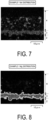
FIG. 7 is a diagram showing a Mn distribution in a cross-sectional view in the vicinity of the surface of the ceramic structure according to Example 1. -
FIG. 8 is a diagram showing a Mg distribution in a cross-sectional view in the vicinity of the surface of the ceramic structure according to Example 1. -
FIG. 9 is a diagram showing a SEM photograph of a cross-sectional view in the vicinity of a surface of the ceramic structure according to Reference Example 1. -
FIG. 10 is a diagram showing an Al distribution in a cross-sectional view in the vicinity of the surface of the ceramic structure according to Reference Example 1. -
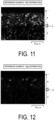
FIG. 11 is a diagram showing a Mn distribution in a cross-sectional view in the vicinity of the surface of the ceramic structure according to Reference Example 1. -
FIG. 12 is a diagram showing a Mg distribution in a cross-sectional view in the vicinity of the surface of the ceramic structure according to Reference Example 1. - Hereinafter, embodiments of a ceramic structure disclosed in the present disclosure will be described with reference to the accompanying drawings. The present disclosure is not limited by the following embodiments. Embodiments can be appropriately combined so as not to contradict each other in terms of processing content. In the following embodiments, the same portions are denoted by the same reference signs, and redundant explanations are omitted.
- In the embodiments described below, expressions such as "constant", "orthogonal", "perpendicular", or "parallel" may be used, but these expressions do not need to be strictly "constant", "orthogonal", "perpendicular", or "parallel". That is, each of the expressions described above allows deviations in, for example, manufacturing accuracy, installation accuracy, and the like.
- Ceramics are widely used for structures from the perspectives of strength, insulation, heat resistance, and the like. As the ceramic structure, a structure in which a metallization layer is provided on a surface of a base made of a ceramic is known.
- However, in the related art, there is room for further improvement in terms of improving adhesion between the base made of a ceramic and the metallization layer. Thus, a technique is expected to overcome the aforementioned problem and improve the adhesion between the base made of a ceramic and the metallization layer in the ceramic structure.
-
FIG. 1 is a schematic perspective view of aceramic structure 1 according to an embodiment, andFIG. 2 is an enlarged cross-sectional view illustrating the example of the configuration of theceramic structure 1 according to the embodiment. Note thatFIG. 2 is a cross-sectional view taken along line A-A illustrated inFIG. 1 . - As illustrated in
FIGs. 1 and 2 , theceramic structure 1 according to the embodiment includes abase 2, afirst layer 3, and asecond layer 4. Thebase 2 has, for example, a rectangular parallelepiped shape and has asurface 2a. Note that in the present disclosure, the shape of thebase 2 is not limited to the example illustrated inFIG. 2 , and may be any shape such as a plate shape, a frame shape, or a pillar shape. - The
base 2 is a sintered ceramic body. Examples of the ceramic constituting thebase 2 include ceramics containing aluminum oxide (Al2O3), silicon carbide (SiC), silicon carbonitride (SiCN), titanium carbide (TiC), and titanium carbonitride (TiCN) as main components. - Note that in the present disclosure, the term "main component" refers to a component that accounts for 80 mass% or more of a total 100 mass% of the components constituting the ceramic. Each of components contained in the ceramic may be identified with an X-ray diffractometer using CuKα rays, and a content of each component may be determined, for example, with an inductively coupled plasma (ICP) optical emission spectrometer or an X-ray fluorescence analyzer.
- The
base 2 containing aluminum oxide as the main component exhibits excellent mechanical characteristics while being relatively inexpensive in terms of raw material cost and manufacturing cost as well among ceramics. - The
base 2 containing aluminum oxide as the main component may further contain, for example, oxides of magnesium (Mg), calcium (Ca), and silicon (Si). - As illustrated in
FIG. 2 , thefirst layer 3 is positioned to be in contact with thesurface 2a of thebase 2. Thefirst layer 3 is made of a ceramic having a composition different from that in thebase 2. Constituent elements of thefirst layer 3 may include, for example, at least one element contained in thebase 2 and at least one element contained in thesecond layer 4. - The
second layer 4 is positioned to be in contact with asurface 3a of thefirst layer 3. Thesecond layer 4 is made of metal and is also referred to as a metallization layer. Thesecond layer 4 may be formed from, for example, a metal material such as molybdenum (Mo), manganese (Mn), tungsten (W), copper (Cu), silver (Ag), palladium (Pd), gold (Au), or platinum (Pt), or an alloy of these metal materials. - The
second layer 4 may contain, for example, molybdenum and manganese. Thus, thesecond layer 4, which is a metal layer, can be formed with good adhesion to thebase 2 made of a ceramic. - The
second layer 4 can be formed by, for example, applying a metal paste prepared by kneading powder of the above metal material together with an organic solvent, a binder, and the like to a ceramic green sheet that serves as thebase 2, and simultaneously sintering the ceramic green sheet with the metal paste in a reducing atmosphere. At this time, thefirst layer 3, which is an intermediate layer, is formed at an interface between thebase 2 and thesecond layer 4. - Note that although the example in
FIGs. 1 and 2 illustrates an example in which thesecond layer 4 is exposed, the present disclosure is not limited to this example, and another layer such as nickel (Ni) plating may be provided on a surface of thesecond layer 4. - In the embodiment, in a cross section intersecting the
surface 2a of thebase 2, that is, a cross section as illustrated inFIG. 2 , DB is a mean grain size of a main crystal (not illustrated) in thebase 2, D1 to Dn are measured values of thicknesses of thefirst layer 3 measured every 1 µm, and DAVE is a mean value of D1 to Dn. Note that n in Dn is an integer. Note that the main crystal refers to crystals that occupy 50 area% or more in the base. - In the embodiment, the
first layer 3 has irregularities where |Dn - DAVE| is larger than DB/2. Thus, the irregularities in thefirst layer 3, which are larger than a value based on the grain size of the main crystal in thebase 2, enhance an anchor effect of thefirst layer 3 on thesurface 2a of thebase 2. - Therefore, according to the embodiment, since the adhesion of the
first layer 3 to thebase 2 can be enhanced, the adhesion between thebase 2 and thesecond layer 4 can be improved. When a minimum contact width between thebase 2 and thefirst layer 3 is 1 mm or more, the adhesion is particularly high. From the viewpoint of adhesion, the minimum contact width may be 2 mm or more, and even 3 mm or more. - In the embodiment, the main crystal of the
base 2 may be aluminum oxide. That is, the main component of thebase 2 may be aluminum oxide. Thus, theceramic structure 1 can exhibit excellent mechanical characteristics while being relatively inexpensive in terms of raw material cost and manufacturing cost as well. - In the embodiment, the constituent elements of the
first layer 3 may include at least one element contained in thebase 2 and at least one element contained in thesecond layer 4. For example, when thebase 2 contains Al, Mg, Ca, Si, and oxygen (O) and thesecond layer 4 contains Mo and Mn, thefirst layer 3 may contain Mg, Al, Mn, and O. - Thus, the
first layer 3, which is the intermediate layer, contains both the elements contained in thebase 2 and thesecond layer 4, thereby the adhesion between thebase 2 and thefirst layer 3 and the adhesion between thefirst layer 3 and thesecond layer 4 can be improved. - Consequently, according to the embodiment, the adhesion between the
base 2 and thesecond layer 4 can be further improved. - In the embodiment, the
first layer 3 may contain crystals having a spinel crystal structure. For example, when thebase 2 contains Al, Mg, Ca, Si, and O, and thesecond layer 4 contains Mo and Mn, thefirst layer 3 may contain at least either of MgO·Al2O3 spinel crystals and MnO·Al2O3 spinel crystals. - Thus, a thermal expansion coefficient of the
base 2 containing aluminum oxide as a main component and a thermal expansion coefficient of thefirst layer 3 containing the spinel crystals described above can be made close to each other. Consequently, according to the embodiment, peeling between thebase 2 and thesecond layer 4 due to thermal cycles can be reduced. - In the embodiment, as illustrated in
FIG. 1 , a thickness t of thebase 2 when thesecond layer 4 is placed on an upper surface thereof may be 2.0 mm or more. Thus, theceramic structure 1 having high insulation properties with respect to thesecond layer 4, which is the metallization layer, can be achieved. - Examples of the present disclosure will be specifically described below. Note that in the examples described below, the
base 2 containing aluminum oxide as a main crystal is described, but the present disclosure is not limited to the following examples. - First, powders of aluminum oxide, which is the main component of the
base 2, and powders of silicon oxide (SiO2), magnesium oxide (MgO), and calcium oxide (CaO) as sintering aids, were prepared. Then, the powders of aluminum oxide and the powders of the sintering aids were mixed so as to be Al2O3: 90 mass%, SiO2: 7 mass%, MgO: 2 mass%, and CaO: 1 mass%, and water and a dispersant were added, and then the mixture is mixed for a predetermined period of time using a ball mill, a bead mill, or the like to obtain a primary slurry. - Subsequently, an organic binder was added to and mixed with the obtained primary slurry to obtain a secondary slurry. Then, the obtained secondary slurry was spray-dried to obtain granules containing aluminum oxide as a main component.
- Subsequently, the obtained granules were filled into a predetermined molding die and press-molded into a predetermined shape, for example, a rectangular parallelepiped shape, under an appropriately set pressure to obtain a green body that serves as the
base 2. - In parallel with the steps of preparing the green body that serves as the
base 2, a metal paste that serves as thesecond layer 4 was prepared. To be specific, first, powders of molybdenum and manganese that constitute thesecond layer 4 and powders of titanium oxide (TiO2) as a sintering aid were prepared. - Then, the powders of molybdenum and manganese and the powders of the sintering aid were mixed so as to be Mo: 85 mass%, Mn: 10 mass%, and TiO2: 5 mass%, and an organic binder was further added and mixed to obtain a metal paste.
- Subsequently, the metal paste was printed on a surface of the green body by a screen printing method, and sintered in a reducing atmosphere, for example, an atmosphere of 20% hydrogen and 80% nitrogen, for a predetermined period of time to obtain three samples to be Examples 1 to 3. Note that a sintering temperature in the sintering step was, for example, 1420°C.
- First, powders of aluminum oxide, which is the main component of the
base 2, and powders of silicon oxide (SiO2), magnesium oxide (MgO), and calcium oxide (CaO) as sintering aids, were prepared. Then, the powders of aluminum oxide and the powders of the sintering aids were mixed so as to be Al2O3: 90 mass%, SiO2: 7 mass%, MgO: 2 mass%, and CaO: 1 mass%, and water and a dispersant were added, and then the mixture is mixed for a predetermined period of time using a ball mill, a bead mill, or the like to obtain a primary slurry. - Subsequently, an organic binder was added to and mixed with the obtained primary slurry to obtain a secondary slurry. Then, the obtained secondary slurry was spray-dried to obtain granules containing aluminum oxide as a main component.
- Subsequently, the obtained granules were filled into a predetermined molding die and press-molded into a predetermined shape, for example, a rectangular parallelepiped shape, under an appropriately set pressure. Then, the obtained molded body was primarily sintered in air to obtain a primary sintered body that serves as the
base 2. Note that a sintering temperature in a primary sintering step was, for example, 1420°C. - In parallel with the steps of preparing the primary sintered body that serves as the
base 2, a metal paste that serves as thesecond layer 4 was prepared. To be specific, first, powders of molybdenum and manganese that constitute thesecond layer 4 and powders of titanium oxide (TiO2) as a sintering aid were prepared. - Then, the powders of molybdenum and manganese and the powders of the sintering aid were mixed so as to be Mo: 85 mass%, Mn: 10 mass%, and TiO2: 5 mass%, and an organic binder was further added and mixed to obtain a metal paste.
- Subsequently, the metal paste was printed on a surface of the primary sintered body by a screen printing method, and secondary-sintered in a reducing atmosphere, for example, an atmosphere of 20% hydrogen and 80% nitrogen, for a predetermined period of time to obtaining three samples to be Reference Examples 1 to 3. Note that a sintering temperature in the secondary sintering step was, for example, 1350°C.
- For each of the
ceramic structures 1 of Examples 1 to 3 and Reference Examples 1 to 3 obtained above, a surface of thebase 2 exposed to a side surface or the like was observed using a scanning electron microscope (SEM).FIG. 3 is a diagram showing a SEM photograph of a base surface of theceramic structure 1 of Example 1, andFIG. 4 is a diagram showing a SEM photograph of a base surface of theceramic structure 1 of Reference Example 1. - Then, using the obtained SEM photograph, the mean grain size DB of aluminum oxide, which is the main crystal of the
base 2, for each of Examples 1 to 3 and Reference Examples 1 to 3 was measured by a code method. To be specific, first, lines are drawn so as to divide the SEM image to be measured into five or more equal parts in a vertical direction and a horizontal direction. For each line, the number of grains in contact with that line is then counted. - Subsequently, the grain size of the grains is calculated from the counted number and a scale bar. Finally, a mean value of all the calculated grain sizes was defined as the mean grain size DB of the main crystal. Note that grains that were partially invisible in the photograph were excluded from the measurement.
- For each of the
ceramic structures 1 of Examples 1 to 3 and Reference Examples 1 to 3 obtained above, the adhesive strength of thesecond layer 4 to thebase 2 was also measured by a peel strength measurement method. First, samples for measurement were prepared. To be specific, nickel plating was formed on the surface of thesecond layer 4, and Kovar was brazed to a surface of the nickel plating with Ag solder. - Subsequently, the sample with brazed Kovar was set in a jig, and one end of a Kovar lead was chucked with a jig. Then, the
second layer 4 was peeled from one end, and the adhesive strength was measured at five points every 1 mm from any position during peeling, and values were read. The adhesive strength was measured using a 98 N load cell and at a crosshead speed of 10 mm/min. - Then, a mean value of the measured values at five points was defined as the adhesive strength per measurement. Further, this measurement was performed 5 to 10 times, and a mean value of the adhesive strengths was defined as the adhesive strength of the sample. Note that a unit of the adhesive strength is N.
- Each of the
ceramic structures 1 of Examples 1 to 3 and Reference Examples 1 to 3 obtained above was cut, a cut surface was mirror-polished, and cross-sections of thebase 2, thefirst layer 3, and thesecond layer 4 were observed using a SEM. Various elements were mapped using an electron probe micro analyzer (EPMA) in a visual field observed using a SEM. -
FIG. 5 is a diagram showing a SEM photograph in a cross-sectional view in the vicinity of a surface of theceramic structure 1 of Example 1.FIGs. 6 to 8 are diagrams showing an Al distribution, a Mn distribution, and a Mg distribution, respectively, in a cross-sectional view in the vicinity of the surface of theceramic structure 1 of Example 1. -
FIG. 9 is a diagram showing a SEM photograph in a cross-sectional view in the vicinity of a surface of theceramic structure 1 of Reference Example 1.FIGs. 10 to 12 are diagrams showing an Al distribution, a Mn distribution, and a Mg distribution, respectively, in a cross-sectional view in the vicinity of the surface of theceramic structure 1 of Reference Example 1. - As shown in
FIGs. 6 to 8 , in theceramic structures 1 of Examples 1 to 3, thefirst layer 3, which is the intermediate layer, containing Al and Mg contained in thebase 2 and Mn contained in thesecond layer 4 is formed between thebase 2 and thesecond layer 4. - As shown in
FIGs. 6 to 8 , thefirst layer 3, which is the intermediate layer, is formed with a larger film thickness in theceramic structures 1 of Examples 1 to 3 than in theceramic structures 1 of Reference Examples 1 to 3 shown inFIGs. 10 to 12 . - As shown in
FIGs. 6 to 8 , thefirst layer 3, which is the intermediate layer, has a complicated shape, that is, a shape with large irregularities, in theceramic structures 1 of Examples 1 to 3 than in theceramic structures 1 of Reference Examples 1 to 3. - Regarding these, it is presumed that by applying the metal paste to the surface of the green body and sintering this green body with the metal paste at the same time, movement of elements at the interface between the
base 2 and thesecond layer 4 becomes easier than by applying the metal paste to the surface of the sintered body and sintering the metal paste separately. - For each of the
ceramic structures 1 of Examples 1 to 3 and Reference Examples 1 to 3, using mapping images of the Al distribution, the Mn distribution, and the Mg distribution, a portion where the three elements were present was regarded as thefirst layer 3, and the thicknesses D1 to Dn of thefirst layer 3 were measured at 20 points every 1 µm. - Note that in this case, color images directly obtained from the analyzer were used as the mapping images of the Al distribution, the Mn distribution, and the Mg distribution, instead of the gray images shown in
FIGs. 6 to 8 and10 to 12 . - Then, a mean value DAVE of the thickness of the
first layer 3 was determined using the obtained thicknesses D1 to Dn, and an absolute value |Dn - DAVE| of a difference between each of the thicknesses D1 to Dn and the mean value DAVE was determined. - For each of Examples 1 to 3 and Reference Examples 1 to 3, the adhesive strength of the sample, the mean grain size DB of the main crystal, thicknesses Dn and |Dn - DAVE| at 20 points in the
first layer 3, mean values, maximum values, minimum values, and standard deviations σ of Dn and |Dn - DAVE|, and the number of measurement points where |Dn - DAVE| is larger than DB/2 (where DB is the mean grain size) are shown in Table 1. Note that the results in Table 1 are values obtained by manually measuring the thicknesses D1 to Dn from the color images obtained from the analyzer. In Table 1, values of the measurement points where |Dn - DAVE| is larger than DB/2 (where DB is the mean grain size) are surrounded by thick frames. -
(Table 1) Example 1 Example 2 Example 3 Reference Example 1 Reference Example 2 Reference Example 3 Adhesive strength (N) 98 95 108 48 53 58 Mean grain size DB (µm) 1.9 1.9 1.9 1.8 1.8 1.8 Measurement point Dn |Dn - DAVE| Dn |Dn - DAVE| Dn |Dn - DAVE| Dn |Dn - DAVE| Dn |Dn - DAVE| Dn |Dn - DAVE| 1 3.30 0.76 2.73 0.35 3.66 0.39 0.77 0.05 0.98 0.02 1.13 0.26 2 3.64 0.42 3.91 0.83 3.66 0.39 0.65 0.17 0.79 0.17 0.86 0.01 3 409 0.03 1.89 1.19 2.27 1.00 0.81 0.01 0.93 0.03 0.65 0.22 4 5.61 1.55 4.44 1.36 3.34 0.07 0.58 0.24 1.02 0.06 0.65 0.22 5 4.62 0.56 3.69 0.61 6.48 3.21 0.65 0.17 0.93 0.03 0.65 0.22 6 3.48 0.58 3.03 0.05 2.27 1.00 1.27 0.45 0.93 0.03 0.65 0.22 7 4.20 0.14 4.44 1.36 2.50 0.77 0.77 0.05 0.74 0.22 0.86 0.01 8 3.83 0.23 2.29 0.79 2.15 1.12 0.77 0.05 0.93 0.03 0.79 0.08 9 6.78 2.72 1.58 1.50 3.42 0.15 0.50 0.32 1.11 0.15 0.65 0.22 10 2.88 1.18 1.27 1.81 5.01 1.74 0.62 0.20 0.84 0.12 1.23 0.36 11 3.52 0.54 2.99 0.09 3.10 0.17 0.85 0.03 0.84 0.12 1.13 0.26 12 3.22 0.84 2.46 0.62 3.78 0.51 1.31 0.49 1.49 0.53 0.86 0.01 13 4.28 0.22 3.30 0.22 1.95 1.32 0.81 0.01 0.84 0.12 0.86 0.01 14 3.22 0.84 3.96 0.88 2.82 0.45 0.92 0.10 0.93 0.03 0.79 0.08 15 3.98 0.08 3.60 0.52 4.21 0.94 0.77 0.05 1.11 0.15 0.93 0.06 16 4.36 0.30 2.02 1.06 3.50 0.23 0.50 0.32 0.60 0.36 0.69 0.18 17 3.98 0.08 4.04 0.96 4.21 0.94 0.85 0.03 0.74 0.22 1.51 0.64 18 4.47 0.41 2.77 0.31 3.42 0.15 0.85 0.03 1.11 0.15 0.65 0.22 19 3.67 0.39 2.29 0.79 2.50 0.77 0.69 0.13 0.84 0.12 0.51 0.36 20 4.05 0.01 4.88 1.80 1.23 204 1.46 0.64 1.49 0.53 1.37 0.50 Mean value (µm) 4.06 0.59 3.08 0.85 3.27 0.87 0.82 0.18 0.96 0.16 0.87 0.21 Maximum value (µm) 6.78 2.72 4.88 1.81 6.48 3.21 1.46 0.64 1.49 0.53 1.51 0.64 Minimum value (µm) 2.88 0.01 1.27 0.05 1.23 0.07 0.50 0.01 0.60 0.02 0.51 0.01 σ (µm) 0.88 0.64 1.02 0.53 1.18 0.77 0.26 0.18 0.22 0.15 0.27 0.17 Number satisfying |Dn - DAVE| > DB/2 3 8 7 0 0 0 - Comparison of Examples 1 to 3 with Reference Examples 1 to 3 shows that the adhesive strength of the
second layer 4 to thebase 2 is improved in Examples 1 to 3 compared to Reference Examples 1 to 3. - Comparison of Examples 1 to 3 with Reference Examples 1 to 3 shows that in Examples 1 to 3, compared to Reference Examples 1 to 3, the
first layer 3 has more irregularities where |Dn - DAVE| is larger than DB/2. - That is, in the embodiment, since the
first layer 3 has many irregularities where |Dn - DAVE| is larger than DB/2, the anchor effect of thefirst layer 3 on thesurface 2a of thebase 2 can be enhanced. Therefore, the adhesion between thebase 2 and thesecond layer 4, that is, the adhesive strength, can be improved. - Comparison of Examples 1 to 3 with Reference Examples 1 to 3 shows that the anchor effect of the
first layer 3 on thesurface 2a of thebase 2 can be further enhanced by having three or more irregularities where |Dn - DAVE| is larger than DB/2. Therefore, the adhesion between thebase 2 and thesecond layer 4, that is, the adhesive strength, can be further improved. - For each of the
ceramic structures 1 of Examples 1 to 3 and Reference Examples 1 to 3, thicknesses D1 to Dn of thefirst layer 3 were measured at 40 points every 1 µm, and a minimum value y1 and a maximum value y2 were measured using image analysis software Image Pro ver. 10 manufactured by Media Cybernetics, Inc. - The minimum value y1 is a value of a minimum coordinate position in a layering direction at the interface between the
base 2 and thefirst layer 3, here, in the vertical direction in the SEM image. The maximum value y2 is a value of a maximum coordinate position in a layering direction at the interface between thefirst layer 3 and thesecond layer 4. - Note that in this case, a SEM image in a different visual field from the SEM image in the visual field used when obtaining the measurement results shown in Table 1 was used. The specific steps are as follows.
- First, open an image to be analyzed. Subsequently, calibrate the image according to a scale of the image using "Create Calibration Data" on the "Home" tab. As the scale of the image, a SEM photograph with a magnification of 1000 to 5000 times may be used depending on a state of the interface. Note that this time, a SEM image with a scale of 3000 times was used.
- Subsequently, create an outline of a boundary portion between the
first layer 3 and thesecond layer 4 by using a function of "Measurement Shapes-Auto Trace Freeform Curves" on the "Measurement" tab. In addition, create an outline of a boundary portion between thefirst layer 3 and thebase 2 by using the function of "Measurement Shapes-Auto Trace Freeform Curves" on the "Measurement" tab. - Subsequently, select the two created outlines using "Select" on the "Measurement" tab. Then, measure the selected two outlines using "Continuous Distance Measurement" on the "Measurement" tab. At this time, a distance of the continuous distance measurement was 1 µm.
- Subsequently, from "Measurement Items" on the "Measurement" tab, add "Line Segment Length", "Line Start Point y", and "Line End Point y" to the measurement items. Then, create a data collection table using "Collection" on the "Measurement" tab.
- Finally, "mean value DAVE", "maximum value of Dn", "minimum value of Dn", and "standard deviation of Dn" were determined from the data recorded in the data collection table. Further, a minimum value of the "Line Start Point y" was defined as a minimum value y1, a maximum value of the "Line End Point y" is defined as a maximum value y2, and a difference between the maximum value y2 and the minimum value y1 is defined as a difference DR. In other words, DR = y2 - y1.
- For each of Examples 1 to 3 and Reference Examples 1 to 3, an adhesive strength of the sample, the mean value, the maximum value, the minimum value, and the standard deviation σ of the thicknesses Dn, and the difference DR are shown in Table 2.
- For each of Examples 1 to 3 and Reference Examples 1 to 3, the adhesive strength of the sample, and a mean grain size DB of the main crystal, thicknesses Dn and |Dn - DAVE| at 40 points in the
first layer 3, the mean values, the maximum values, the minimum values, and the standard deviations σ of Dn and |Dn - DAVE|, and the number of measurement points where |Dn - DAVE| is larger than DB/2 (where DB is the mean grain size) measured using image analysis software Image Pro ver. 10 manufactured by Media Cybernetics, Inc. are shown in Table 3. Note that in Table 3, the values of the measurement points where |Dn - DAVE| is larger than DB/2 (where DB is the mean grain size) are surrounded by thick frames. -
(Table 2) Example 1 Example 2 Example 3 Reference Example 1 Reference Example 2 Reference Example 3 Adhesive strength (N) 98 95 108 48 53 58 DAVE(µm) 4.47 3.34 3.23 0.59 0.58 0.57 Maximum value Dn (µm) 7.02 5.01 6.37 1.67 1.68 2.12 Minimum value Dn (µm) 2.83 0.68 1.14 0.25 0.35 0.24 Dn σ (µm) 1.22 1.03 0.85 0.30 0.24 0.38 DR (µm) 8.63 7.15 8.10 3.11 3.19 3.25 -
(Table 3) Example 1 Example 2 Example 3 Reference Example 1 Reference Example 2 Reference Example 3 Adhesive strength (N) 98 95 108 48 53 58 Mean grain size DB (µm) 1.9 1.9 1.9 1.8 1.8 1.8 Measurement point Dn |Dn - DAVE| Dn |Dn - DAVE| Dn |Dn - DAVE| Dn |Dn - DAVE| Dn |Dn - DAVE| Dn |Dn - DAVE| 1 4.23 0.24 1.00 2.35 3.59 0.36 0.39 0.21 1.68 1.09 1.07 0.49 2 4.48 0.01 0.76 2.58 3.33 0.10 0.58 0.01 0.71 0.13 1.07 0.49 3 3.68 0.79 0.68 2.66 3.49 0.26 0.38 0.21 0.54 0.04 0.50 0.08 4 3.61 0.86 2.30 1.05 2.08 1.15 0.46 0.13 0.47 0.11 0.41 0.16 5 6.14 1.67 3.14 0.20 3.25 0.03 0.38 0.21 0.51 0.07 0.53 0.04 6 6.53 206 3.10 0.24 3.75 0.52 0.32 0.27 0.85 0.27 0.53 004 7 6.69 2.22 2.50 0.85 3.36 0.13 0.51 0.09 0.48 0.10 0.89 0.31 8 4.56 0.09 2.55 0.80 3.64 0.41 0.43 0.17 0.50 0.08 0.47 0.10 9 3.89 0.58 2.35 1.00 3.39 0.16 0.38 0.22 0.77 0.19 0.65 0.08 10 3.62 0.85 2.88 0.47 3.68 0.45 0.95 0.36 0.81 0.23 0.47 0.10 11 6.51 204 4.09 0.75 3.82 0.59 0.39 0.21 0.43 0.15 1.64 1.07 12 6.88 2.41 4.02 0.67 3.64 0.41 0.64 0.05 0.41 0.17 0.37 0.20 13 6.33 1.86 4.16 0.82 3.53 0.30 1.34 0.75 0.71 0.13 0.35 0.22 14 5.54 1.07 4.42 1.08 2.03 1.20 0.38 0.21 0.72 0.13 0.59 0.02 15 4.58 0.11 3.74 0.39 2.64 0.59 0.57 0.02 0.77 0.19 0.30 0.28 16 4.24 0.23 3.96 0.62 2.46 0.77 0.62 0.02 0.47 0.11 0.32 0.26 17 3.95 0.52 3.75 0.41 3.10 0.13 0.38 0.21 0.35 0.23 0.36 0.22 18 4.66 0.19 3.89 0.54 4.69 1.46 0.42 0.17 0.52 0.06 0.41 0.16 19 5.99 1.52 3.82 0.48 6.37 3.14 0.47 0.12 0.35 0.23 0.36 0.22 20 4.23 0.24 4.39 1.05 3.43 0.20 1.08 0.49 0.59 0.01 0.41 0.16 21 3.87 0.60 2.78 0.57 3.75 0.52 0.48 0.11 0.35 0.23 0.34 0.23 22 3.07 1.40 3.71 0.37 3.60 0.37 0.56 0.03 0.38 0.20 0.24 0.34 23 4.49 0.02 4.67 1.33 3.69 0.46 0.57 0.02 0.41 0.17 0.54 0.04 24 5.46 0.99 4.09 0.75 1.79 1.44 0.67 0.07 0.53 0.05 0.41 0.16 25 7.02 2.55 3.40 0.05 2.07 1.16 0.83 0.24 0.59 0.01 0.53 0.04 26 5.54 1.07 3.65 0.31 2.52 0.71 0.53 0.06 0.47 0.11 0.51 0.06 27 2.83 1.64 2.92 0.43 2.17 1.06 0.37 0.22 0.43 0.15 0.25 0.33 28 3.08 1.39 3.39 0.04 2.57 0.66 0.25 0.34 0.48 0.10 0.36 0.22 29 3.08 1.39 2.80 0.54 2.93 0.30 0.50 0.09 0.47 0.11 0.53 0.04 30 3.08 1.39 2.75 0.60 2.86 0.37 0.38 0.21 0.83 0.24 0.65 0.08 31 3.34 1.13 2.33 1.01 3.60 0.37 1.67 1.08 0.47 0.11 1.07 0.50 32 3.70 0.77 2.84 0.50 4.36 1.13 0.63 0.04 0.41 0.17 0.59 0.02 33 3.61 0.86 4.08 0.73 2.83 0.40 0.63 0.03 0.71 0.13 0.42 0.16 34 3.61 0.86 4.08 0.73 3.21 0.02 0.51 0.09 0.41 0.17 0.30 0.28 35 3.52 0.95 4.62 1.28 3.65 0.42 0.57 0.02 0.59 0.01 0.30 0.28 36 4.04 0.43 3.49 0.14 3.86 0.63 1.34 0.75 0.58 0.00 0.30 0.28 37 4.49 0.02 3.23 0.11 2.99 0.24 0.82 0.22 1.06 0.48 0.41 0.16 38 3.78 0.69 3.48 0.14 2.95 0.28 0.44 0.15 0.58 0.00 2.12 1.55 39 3.53 0.94 4.94 1.60 2.57 0.66 0.51 0.09 0.45 0.14 0.36 0.22 40 3.34 1.13 5.01 1.67 1.93 1.30 0.38 0.21 0.42 0.16 1.02 0.45 Mean value (µm) 4.47 0.99 3.34 0.80 3.23 0.62 0.59 0.21 0.58 0.16 0.57 0.25 Maximum value (µm) 7.02 2.55 5.01 2.66 6.37 3.14 1.67 1.08 1.68 1.09 2.12 1.55 Minimum value (µm) 2.83 0.01 0.68 0.44 1.79 0.02 0.25 0.01 0.35 0.00 0.24 0.02 σ (µm) 1.22 0.69 1.03 0.64 0.85 0.57 0.30 0.22 0.24 0.18 0.38 0.28 Number satisfying |Dn - DAVE| > DB/2 19 12 9 1 1 2 - Comparison of Examples 1 to 3 with Reference Examples 1 to 3 shows that when the value of the difference DR is 4 µm or more, the anchor effect of the
first layer 3 on thesurface 2a of thebase 2 can be enhanced, thereby improving the adhesion between thebase 2 and thesecond layer 4, that is, the adhesive strength. - Comparison of Examples 1 to 3 with Reference Examples 1 to 3 shows that when the value of the difference DR is 7 µm or more, the anchor effect of the
first layer 3 on thesurface 2a of thebase 2 can be further enhanced, thereby further improving the adhesion between thebase 2 and thesecond layer 4, that is, the adhesive strength. - X-ray diffraction analysis (XRD) was performed on a mirror-polished cross-sectional sample of the
ceramic structure 1 of each of Examples 1 to 3 and Reference Examples 1 to 3 obtained above to evaluate crystalline states of the vicinity of thefirst layer 3 and thebase 2. - As a result, it was found that in each of Examples 1 to 3 and Reference Examples 1 to 3, the
base 2 contained 97.8 mass% of aluminum oxide as a main phase and 2.2 mass% of sapphirine as a different phase. - In Examples 1 to 3, the vicinity of the
first layer 3 contained 94.0 mass% of aluminum oxide and 6.0 mass% of spinel. On the other hand, in Reference Examples 1 to 3, the vicinity of thefirst layer 3 contained 98.3 mass% of aluminum oxide and 1.7 mass% of sapphirine. - That is, in Examples 1 to 3, it was found that the
first layer 3 contained crystals having a spinel crystal structure. This can reduce peeling between thebase 2 and thesecond layer 4 due to thermal expansion and thermal contraction. - Although the embodiment of the present disclosure has been described above, the present disclosure is not limited to the embodiment described above, and various changes can be made without departing from the spirit of the present disclosure.
- Additional effects and other aspects can be easily derived by a person skilled in the art. Thus, a wide variety of aspects of the present disclosure are not limited to the specific details and representative embodiments represented and described above. Accordingly, various changes are possible without departing from the spirit or scope of the general inventive concepts defined by the appended claims and their equivalents.
-
- 1 Ceramic structure
- 2 Base
- 2a Surface
- 3 First layer
- 3a Surface
- 4 Second layer
Claims (8)
- A ceramic structure comprising:a base comprising a ceramic;a first layer positioned to be in contact with a surface of the base, the first layer comprising a ceramic having a composition different from a composition in the base; anda second layer positioned to be in contact with a surface of the first layer, the second layer comprising a metal,wherein in a cross section intersecting the surface of the base, whenDB is a mean grain size of a main crystal in the base,D1 to Dn are measured values of thicknesses of the first layer measured every 1 µm, andDAVE is a mean value of the D1 to Dn,the first layer has irregularities where |Dn - DAVE| is larger than DB/2.
- A ceramic structure comprising:a base comprising a ceramic;a first layer positioned to be in contact with a surface of the base, the first layer comprising a ceramic having a composition different from a composition in the base; anda second layer positioned to be in contact with a surface of the first layer, the second layer comprising a metal,wherein in a cross section intersecting the surface of the base, wheny1 is a minimum value of a coordinate position in a layering direction at an interface between the base and the first layer,y2 is a maximum value of a coordinate position in a layering direction at an interface between the first layer and the second layer, andDR is a difference between the y2 and the y1,the DR is 4 µm or more.
- The ceramic structure according to claim 2, wherein
the DR is 7 µm or more. - The ceramic structure according to claim 2 or 3, whereinwhen DB is a mean grain size of a main crystal in the base,D1 to Dn are measured values of thicknesses of the first layer measured every 1 µm, andDAVE is a mean value of the D1 to Dn,the first layer has irregularities where |Dn - DAVE| is larger than DB/2.
- The ceramic structure according to claim 1 or 4, wherein
in a measurement range of n = 20, the number of the irregularities is three or more. - The ceramic structure according to any one of claims 1 to 5, wherein
the main crystal in the base is aluminum oxide. - The ceramic structure according to any one of claims 1 to 6, wherein
constituent elements of the first layer comprise at least one element contained in the base and at least one element contained in the second layer. - The ceramic structure according to any one of claims 1 to 7, wherein
the first layer comprises crystals having a spinel crystal structure.
Applications Claiming Priority (2)
| Application Number | Priority Date | Filing Date | Title |
|---|---|---|---|
| JP2022052427 | 2022-03-28 | ||
| PCT/JP2023/012448 WO2023190484A1 (en) | 2022-03-28 | 2023-03-28 | Ceramic structure |
Publications (2)
| Publication Number | Publication Date |
|---|---|
| EP4501893A1 true EP4501893A1 (en) | 2025-02-05 |
| EP4501893A4 EP4501893A4 (en) | 2026-04-15 |
Family
ID=88202474
Family Applications (1)
| Application Number | Title | Priority Date | Filing Date |
|---|---|---|---|
| EP23780493.5A Pending EP4501893A4 (en) | 2022-03-28 | 2023-03-28 | CERAMIC STRUCTURE |
Country Status (4)
| Country | Link |
|---|---|
| EP (1) | EP4501893A4 (en) |
| JP (1) | JP7844624B2 (en) |
| CN (1) | CN118891240A (en) |
| WO (1) | WO2023190484A1 (en) |
Family Cites Families (13)
| Publication number | Priority date | Publication date | Assignee | Title |
|---|---|---|---|---|
| JP2742623B2 (en) * | 1990-01-22 | 1998-04-22 | 京セラ株式会社 | Alumina sintered body having metallized metal layer |
| JPH03275580A (en) * | 1990-03-22 | 1991-12-06 | Kyocera Corp | Aluminous sintered body having metallized metallic layer |
| JP3242458B2 (en) * | 1992-08-18 | 2001-12-25 | 松下電工株式会社 | Manufacturing method of metallized ceramic substrate |
| JP3700150B2 (en) * | 1995-07-31 | 2005-09-28 | 同和鉱業株式会社 | Ceramic multilayer substrate with tab electrode and method for manufacturing the same |
| JP3792283B2 (en) * | 1995-10-30 | 2006-07-05 | 京セラ株式会社 | Manufacturing method of ceramic substrate |
| JP3301914B2 (en) * | 1996-04-23 | 2002-07-15 | 京セラ株式会社 | Wiring board |
| JP3488794B2 (en) * | 1996-12-27 | 2004-01-19 | 京セラ株式会社 | Aluminum nitride metallized substrate and method of manufacturing the same |
| JP4753469B2 (en) * | 2000-12-26 | 2011-08-24 | 京セラ株式会社 | Wiring board and manufacturing method thereof |
| JP4428890B2 (en) * | 2001-06-22 | 2010-03-10 | 日本特殊陶業株式会社 | Ceramic member, joined body, and container for vacuum switch |
| JP4348112B2 (en) | 2003-05-13 | 2009-10-21 | 日本特殊陶業株式会社 | Metallized layer forming ceramic sintered body, metallized paste, and metallized layer forming ceramic sintered body manufacturing method |
| CN102049514B (en) * | 2009-11-11 | 2012-08-01 | 福建泉州万顺捷集团有限公司 | Powder for aluminum oxide ceramics nano metallized paste and preparation method thereof |
| CN110563484A (en) * | 2019-08-26 | 2019-12-13 | 泰州市光明电子材料有限公司 | Ceramic surface metallization process |
| CN110563466A (en) * | 2019-09-25 | 2019-12-13 | 深圳市辰昱科技有限公司 | porous ceramic heating element and preparation method thereof |
-
2023
- 2023-03-28 JP JP2024512548A patent/JP7844624B2/en active Active
- 2023-03-28 EP EP23780493.5A patent/EP4501893A4/en active Pending
- 2023-03-28 CN CN202380027366.5A patent/CN118891240A/en active Pending
- 2023-03-28 WO PCT/JP2023/012448 patent/WO2023190484A1/en not_active Ceased
Also Published As
| Publication number | Publication date |
|---|---|
| CN118891240A (en) | 2024-11-01 |
| WO2023190484A1 (en) | 2023-10-05 |
| EP4501893A4 (en) | 2026-04-15 |
| JPWO2023190484A1 (en) | 2023-10-05 |
| JP7844624B2 (en) | 2026-04-13 |
Similar Documents
| Publication | Publication Date | Title |
|---|---|---|
| US20140285943A1 (en) | Ceramic member and member for semiconductor manufacturing equipment | |
| KR101963521B1 (en) | Ceramic structure, member for substrate holding device, and method for manufacturing ceramic structure | |
| EP2248784B1 (en) | Zirconia sintered body and manufacturing method thereof | |
| EP2546840B1 (en) | Surface-mountable negative-characteristic ceramic thermistor based on Mn, Co, Ni and Ti compounds | |
| JP3629783B2 (en) | Circuit board | |
| KR20130121032A (en) | Alumina sintered body, member including the same, and semiconductor manufacturing apparatus | |
| KR20130118239A (en) | Composite ceramics and a component member for semiconductor manufacturing apparatus | |
| EP3247180A1 (en) | Ceramic substrate | |
| US8735309B2 (en) | Mullite-based sintered body, circuit board using same and probe card | |
| EP1582509B1 (en) | Dense cordierite based sintered body | |
| EP4501893A1 (en) | Ceramic structure | |
| JP7327065B2 (en) | Dielectric compositions and electronic components | |
| JP5725845B2 (en) | Ceramic circuit board for probe card and probe card using the same | |
| JP2021107304A (en) | Dielectric composition and electronic device | |
| JP2003163425A (en) | Wiring board | |
| JP2012047579A (en) | Ceramic wiring board for probe card and probe card employing the same | |
| JP5368052B2 (en) | Multilayer ceramic substrate and manufacturing method thereof | |
| JP5511613B2 (en) | Ceramic circuit board for probe card and probe card using the same | |
| JP5840993B2 (en) | Alumina ceramics and wiring board using the same | |
| JP3389384B2 (en) | Aluminum nitride substrate | |
| EP3831796A1 (en) | Aluminous porcelain and ceramic heater | |
| EP3277063A1 (en) | Circuit substrate and electronic device provided with same | |
| JP2010098049A (en) | Multilayer ceramic substrate and method for manufacturing the same | |
| JP7039075B2 (en) | Conductive material, conductive ceramics, conductive paste, conductive material film, composite oxide manufacturing method, conductive paste manufacturing method and conductive material film manufacturing method | |
| JP3218906B2 (en) | Thermistor element |
Legal Events
| Date | Code | Title | Description |
|---|---|---|---|
| STAA | Information on the status of an ep patent application or granted ep patent |
Free format text: STATUS: THE INTERNATIONAL PUBLICATION HAS BEEN MADE |
|
| PUAI | Public reference made under article 153(3) epc to a published international application that has entered the european phase |
Free format text: ORIGINAL CODE: 0009012 |
|
| STAA | Information on the status of an ep patent application or granted ep patent |
Free format text: STATUS: REQUEST FOR EXAMINATION WAS MADE |
|
| 17P | Request for examination filed |
Effective date: 20240916 |
|
| AK | Designated contracting states |
Kind code of ref document: A1 Designated state(s): AL AT BE BG CH CY CZ DE DK EE ES FI FR GB GR HR HU IE IS IT LI LT LU LV MC ME MK MT NL NO PL PT RO RS SE SI SK SM TR |
|
| DAV | Request for validation of the european patent (deleted) | ||
| DAX | Request for extension of the european patent (deleted) | ||
| REG | Reference to a national code |
Ref country code: DE Ref legal event code: R079 Free format text: PREVIOUS MAIN CLASS: C04B0041880000 Ipc: C04B0041510000 |
|
| A4 | Supplementary search report drawn up and despatched |
Effective date: 20260318 |
|
| RIC1 | Information provided on ipc code assigned before grant |
Ipc: C04B 41/51 20060101AFI20260312BHEP Ipc: C04B 41/88 20060101ALI20260312BHEP Ipc: C04B 41/00 20060101ALI20260312BHEP Ipc: C04B 35/10 20060101ALI20260312BHEP Ipc: C04B 35/117 20060101ALI20260312BHEP |