EP4498526A2 - Rfid-inlay mit einer massefläche - Google Patents
Rfid-inlay mit einer massefläche Download PDFInfo
- Publication number
- EP4498526A2 EP4498526A2 EP24217626.1A EP24217626A EP4498526A2 EP 4498526 A2 EP4498526 A2 EP 4498526A2 EP 24217626 A EP24217626 A EP 24217626A EP 4498526 A2 EP4498526 A2 EP 4498526A2
- Authority
- EP
- European Patent Office
- Prior art keywords
- substrate
- area
- inlay
- rfid inlay
- disposed
- Prior art date
- Legal status (The legal status is an assumption and is not a legal conclusion. Google has not performed a legal analysis and makes no representation as to the accuracy of the status listed.)
- Pending
Links
Images




Classifications
-
- H—ELECTRICITY
- H01—ELECTRIC ELEMENTS
- H01Q—ANTENNAS, i.e. RADIO AERIALS
- H01Q1/00—Details of, or arrangements associated with, antennas
- H01Q1/12—Supports; Mounting means
- H01Q1/22—Supports; Mounting means by structural association with other equipment or articles
- H01Q1/2208—Supports; Mounting means by structural association with other equipment or articles associated with components used in interrogation type services, i.e. in systems for information exchange between an interrogator/reader and a tag/transponder, e.g. in Radio Frequency Identification [RFID] systems
- H01Q1/2225—Supports; Mounting means by structural association with other equipment or articles associated with components used in interrogation type services, i.e. in systems for information exchange between an interrogator/reader and a tag/transponder, e.g. in Radio Frequency Identification [RFID] systems used in active tags, i.e. provided with its own power source or in passive tags, i.e. deriving power from RF signal
-
- G—PHYSICS
- G06—COMPUTING OR CALCULATING; COUNTING
- G06K—GRAPHICAL DATA READING; PRESENTATION OF DATA; RECORD CARRIERS; HANDLING RECORD CARRIERS
- G06K19/00—Record carriers for use with machines and with at least a part designed to carry digital markings
- G06K19/06—Record carriers for use with machines and with at least a part designed to carry digital markings characterised by the kind of the digital marking, e.g. shape, nature, code
- G06K19/067—Record carriers with conductive marks, printed circuits or semiconductor circuit elements, e.g. credit or identity cards also with resonating or responding marks without active components
- G06K19/07—Record carriers with conductive marks, printed circuits or semiconductor circuit elements, e.g. credit or identity cards also with resonating or responding marks without active components with integrated circuit chips
- G06K19/077—Constructional details, e.g. mounting of circuits in the carrier
- G06K19/07749—Constructional details, e.g. mounting of circuits in the carrier the record carrier being capable of non-contact communication, e.g. constructional details of the antenna of a non-contact smart card
- G06K19/07773—Antenna details
- G06K19/0779—Antenna details the antenna being foldable or folded
-
- H—ELECTRICITY
- H01—ELECTRIC ELEMENTS
- H01Q—ANTENNAS, i.e. RADIO AERIALS
- H01Q1/00—Details of, or arrangements associated with, antennas
- H01Q1/08—Means for collapsing antennas or parts thereof
-
- H—ELECTRICITY
- H01—ELECTRIC ELEMENTS
- H01Q—ANTENNAS, i.e. RADIO AERIALS
- H01Q1/00—Details of, or arrangements associated with, antennas
- H01Q1/36—Structural form of radiating elements, e.g. cone, spiral, umbrella; Particular materials used therewith
- H01Q1/38—Structural form of radiating elements, e.g. cone, spiral, umbrella; Particular materials used therewith formed by a conductive layer on an insulating support
-
- H—ELECTRICITY
- H01—ELECTRIC ELEMENTS
- H01Q—ANTENNAS, i.e. RADIO AERIALS
- H01Q9/00—Electrically-short antennas having dimensions not more than twice the operating wavelength and consisting of conductive active radiating elements
- H01Q9/04—Resonant antennas
- H01Q9/30—Resonant antennas with feed to end of elongated active element, e.g. unipole
- H01Q9/40—Element having extended radiating surface
Definitions
- RFID radio frequency identification
- Typical RFID tags or integrated circuits include a microprocessor, also known as a microchip, electrically connected to an antenna.
- the microchip is first attached to a pad having electrical leads that provides a larger attachment of "landing" area. This is typically referred to as a "strap" or "interposer.” The strap is then attached to the antenna.
- the microprocessor stores data, which can include identifying data unique to a specific item, which is transmitted to an external receiver for reading by an operator and processing of the item.
- RFID tags can be attached to or associated with items for inventory control, shipment control, loss prevention, and the like. RFID tags are particularly useful in identifying, tracking and controlling items such as packages, pallets, and other product containers. The location of each item can be tracked and information identifying the owner of the item or specific handling requirements, can be encoded into the chip contained in the RFID tag and later read by a scanning device or reader which is capable of decoding and displaying the information previously encoded on the chip.
- RFID tags can be attached to or associated with items entering or within a supply chain or retail environment and the identifying information received can be processed for various reasons in a variety of manners.
- RFID tags are particularly useful in identifying, tracking and controlling items such as pallets, packages, consumer goods and individual product containers.
- the tuning of an RFID tag can be dependent on the contents of the container. For example, conductive materials or materials having a high dielectric constant, for example, liquids or metals, can detune an RFID tag or substantially interfere with the RFID tag. Consequently, communications with such a tag are difficult and often ineffective.
- an RFID inlay (which is a chip connected to an antenna provided on a substrate) is disclosed.
- the RFID inlay can include a substrate having a first area and a second area, a conductive structure having a first part disposed over at least a portion of the first area and a second part disposed over at least a portion of the second area, and a dielectric material disposed over at least a portion of the conductive structure, wherein the substrate is adapted to be folded such that the first part of the conductive structure is disposed over the second part of the conductive structure and the dielectric material is disposed between the first part and the second part such that the first and second parts are not in contact with one another.
- a RFID inlay can include a first substrate having a first conductive structure disposed thereon, a second substrate having a second conductive structure disposed thereon, the second conductive structure having a first portion and at least one second portion, and a dielectric layer disposed between the first conductive structure and the first portion of the second conductive structure, wherein the at least one second portion of the second conductive structure is capacitively coupled to the first conductive structure.
- a RFID inlay can include a substrate having a first surface and a second surface, a plurality of cuts defined in the substrate so as to partition the substrate into a first area and a second area separable from the first area, a plurality of hinges coupled to the first area and the second area, a first conductive structure disposed on the first surface of the substrate and coextensive with the first area and at least a portion of the second area, and a second conductive structure disposed on the second surface of the substrate and coextensive with the first area.
- an RFID inlay includes a substrate having a conductive pattern disposed thereon, with the conductive pattern having first and second portions.
- a dielectric layer is disposed over the conductive pattern and a transfer tape diposed over a portion of the dielectric layer.
- the substrate is folded over onto itself such that the first and second portions of the conductive pattern are juxtaposed over one another and separated by the dielectric layer.
- each of the first and second patterns have first and second longitudinal edges and first and second transverse edges.
- the first and second transverse edges are in substantial alignment with one another and at least one of the first and second longitudinal edges of each of the first and second patterns is out of alignment with another of the first and second edges of the first and second portions of the conductive pattern.
- the word "exemplary” means “serving as an example, instance or illustration.”
- the embodiments described herein are not limiting, but rather are exemplary only. It should be understood that the described embodiment are not necessarily to be construed as preferred or advantageous over other embodiments.
- the terms “embodiments of the invention”, “embodiments” or “invention” do not require that all embodiments of the invention include the discussed feature, advantage or mode of operation.
- an RFID inlay incorporating a ground plane is disclosed.
- the ground plane can interact with the antenna structure of the RFID inlay so as to mitigate the effects of RFID-unfriendly materials (metals, liquids, etc.) on the performance of the RFID inlay.
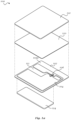
- Figs. 1a-1d show a first exemplary embodiment of an RFID inlay 100.
- the inlay 100 can include a substrate 102 having an antenna structure 104 disposed thereon.
- Substrate 102 can be any material, for example paper, coated paper, films, polyester, polyethylene terephthalate (PET), laminations of film and paper or any other suitable substrate that can be desired.
- Substrate 102 may be divided into a first portion 102a and a second portion 102b.
- Substrate 102 may have a first face 103a on which antenna structure 104 may be disposed, and a second face 103b which may be suitable for printing thereon.
- the substrate 120 is substantially quadrate in shape and is generally larger than the antenna structure104 that is disposed on the substrate. That is the antenna 104 is fully contained within the perimeter of the substrate.
- Other geometric configurations are of course possible.
- the fold line 126 runs substantially medially of the substrate such that portion 114 is has less conductive material making up the antenna portion than antenna portion 116.
- Strap 110 is also shown on portion 114. When folded over, portion 114 does not extend to a longitudinal end edge of portion 116 and portion 116 extends beyond the longitudinal end edge of portion 114. As can be seen from the figures, neither of the longitudinal edges of the antenna portions align with one another when the structure is folded on itself. The transverse edges of portions 114 and 116 are substantially aligned with one another.
- Antenna structure 104 can be any of a variety of materials, for example aluminum, copper, silver or another thin, conductive material, for example etched or hot-stamped metal foil. Antenna structure 104 may be coupled to an RFID integrated circuit 108 that may be part of a strap or interposer 106. Strap or interposer 106 may further include conductive leads 110, 112 to facilitate coupling between antenna structure 104 and integrated circuit 108. In some embodiments, strap or interposer 106 may also include a substrate to facilitate supporting integrated circuit 108 and conductive leads 110. Coupling between antenna structure 104 and strap or interposer 106 may be a direct, conductive coupling or may be an indirect coupling, such as a capacitive or inductive coupling or any combination of conductive, capacitive and inductive coupling.
- Antenna structure 104 may be a continuous, unitary layer of conductive material.
- a slot 112 defined in the antenna structure can partition antenna structure 104 into a first area 114 and a second area 116.
- First area 114 can include a radiating element 114a.
- radiating element 114a may be a monopole.
- Second area 116 of antenna structure 104 can include a first portion 116a disposed over first portion 102a of substrate 102, and a second portion 116b disposed over second portion 102b of substrate 102.
- first area 114 and second area 116 may be conductively coupled by a bridge 118 extending between first portion 116a of second area 116 and a second end 114b of first area 114 disposed opposite the radiating element 114a.
- Slot 112 may also be bridged by strap or interposer 106.
- An overlaminate layer 120 may be disposed over the first face 103a of substrate 102 and antenna structure 104.
- the overlaminate may be a film which may be formed from any suitable material, for example polyester, cellulose acetate, polyethylene, polypropylene or the like and can be adhesively applied to the substrate 102, heat bonded, sonically sealed or otherwise fused together.
- Dielectric layer 122 may be coextensive with antenna structure 104 or substrate 102.
- dielectric layer 122 may have a thickness of approximately 0.5 mm.
- the dielectric layer 122 may be formed from any suitable material.
- the dielectric layer may be formed foam, such as polypropylene foam, or any other low-density structure.
- a thickness of approximately 0.5 mm for dielectric layer 122 is sufficiently thin to allow for the inlay 100 to be received through printing apparatuses.
- both surfaces of dielectric layer 122 may be provided with a self-adhesive coating.
- an adhesive layer 124 may be disposed on the second surface 103b of substrate 102.
- Adhesive layer 124 may be disposed such that it is positioned proximate the second portion 102b of substrate 102.
- Adhesive layer 124 may be any known adhesive, for example a transfer tape, and may be provided with a release layer on the exposed surface thereof.
- RFID inlay 100 may be manufactured in a roll-to-roll manufacturing process, as discussed further below.
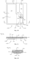
- inlay 100 may have a flat configuration, as shown in Figs. 1b-1c .
- Such a configuration can reduce issues relating to tension and stress on the inlay during the manufacturing process.
- the operation of inlay 100 is likely to be sub-optimal and inefficient if inlay 100 is affixed to an object having conductive materials or materials having a high dielectric constant.
- RFID inlay 100 may be folded along a fold axis 126, shown in Fig. 1b , such that the first portion 102a of substrate 102 is disposed over the second portion 102b of substrate 102.
- inlay 100 when folded, inlay 100 may have a thickness of about 1 mm, a length of about 21 mm and a width of about 46 mm.
- Fig. 1d shows an exemplary embodiment of RFID inlay 100 in a folded configuration.
- the second area 116b of second portion 116 of antenna structure 104 functions as a ground plane element with respect to first portion 114 of antenna structure 104.
- adhesive layer 124 is used to couple inlay 100 to an object
- the second area / ground plane element 116b is consequently disposed between the object and radiating element 114 when inlay 100 is in the folded configuration.
- the presence of a ground plane 116b between the object and radiating element 114 can mitigate the effect of conductive materials or materials having a high dielectric constant on the operation of inlay 100.
- inlay 100 can operate efficiently even when affixed to objects containing such materials.
- the dielectric layer 122 is disposed between the first area 114 of antenna structure 104 and the ground plane element 116b of antenna structure 104.
- the adhesive disposed on the face of dielectric layer 122 can serve to maintain inlay 100 in the folded configuration.
- dielectric layer 122 can serve to prevent undesired interaction between radiating element 114 and ground plane 116b.
- inlay 100 can include two main tuning elements, the first of these tuning elements being radiating element 114a.
- the second tuning element can be a loop formed by the combination of strap 106 and bridge 118. If the total thickness of the substrate drops when inlay 100 is folded, radiating element 114a can act to decrease the radio frequency radiated from antenna structure 104, while the loop can act to increase the radio frequency radiated from antenna structure 104. Consequently, the tuning elements can serve to stabilize the operating point of inlay 100 against variations in the gap between radiating element 114 and ground plane 116 caused by manufacturing tolerances and the properties of the materials used.
- each of the first and second patterns 114, 116 have first and second longitudinal edges and first and second transverse edges (see Figure 1 b) and wherein the first and second transverse edges are in substantial alignment with one another and at least one of the first and second longitudinal edges of each of the first and second patterns 114, 116 is out of alignment with another of the first and second edges of the first and second portions of the conductive pattern.
- Figs. 2a-2c show a second exemplary embodiment of RFID inlay 200.
- substantially similar elements to those in the first exemplary embodiment of inlay 100 are represented by similar numerals, with the leading digit incremented to 2. Thus, a detailed description of the similar elements may be omitted.
- the second exemplary embodiment has substantially similar structure and functionality to the first exemplary embodiment, except for the features described below.
- dielectric layer 222 may overlap a portion of substrate 202 and antenna structure 204, as shown in Figs. 2a-2b .
- dielectric layer 222 may have a thickness of approximately 0.5 mm.
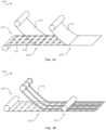
- Figs. 3a-3b show an exemplary schematic of a manufacturing process 300 for the embodiments of inlay 100, 200.
- the schematic illustrates a web to facilitate a roll to roll or continuous process.
- substrate media 102 having a plurality of antenna structures 104 disposed on a first surface 102b of the web thereof may be provided.
- the substrate media may be any suitable material, such as paper or film and as shown in the figure is provided in a continuous format. It should be understood that practice of this invention may also be done in a cut sheet configuration.
- an overlaminate layer 120 may be applied to the first surface of the substrate, on which the antenna structures 104 are disposed.
- a layer of dielectric material 122 such as foam, may be applied over the overlaminate layer.
- the dielectric material may be applied as a sheet or as strips, depending on the embodiment of the inlay that is being manufactured.
- the dielectric and overlaminate may be previously die cut such that upon attachment and alignment over the designated antenna areas, the matrix portion can be readily stripped away leaving a substantially completed assembly on the base or carrier web. Otherwise, the die cutting can occur post application such that the individual RFID inlays can be removed from the web.
- the laminated sheet resulting from step 306 is turned over with the dielectric element 122 now on the bottom of the web.
- strips of transfer tape are applied to the second surface 102b of the substrate media.
- the resulting laminated structure may be die cut into separate inlays.
- the inlays can have a flat configuration. Folding of the inlays may subsequently be performed by a suitable folding apparatus, or by an end user of the inlays.
- the liner on the transfer tape is peeled away such that the substrate can be folded onto itself and secured.
- the transfer tape is only applied to one side of the RFID inlay or covers only one portion of the antenna structure.
- FIGS 4a-4c show a third exemplary embodiment of an inlay 400.
- the inlay 400 can include a substrate 402 having a ground plane 416 disposed on a first surface 403a thereof, an adhesive layer 424 disposed over the ground plane 416, an antenna structure 404 provided separately from the ground plane 416 and disposed over the adhesive layer 424, and a dielectric layer 422 disposed between a portion of the antenna structure 404 and the dielectric layer 422.
- Substrate 402 can be any material, for example paper, coated paper, polyethylene terephthalate (PET), laminations of film and paper or any other suitable substrate that can be desired.
- a bottom surface 403b of the substrate may include an adhesive covered by a release layer so as to allow coupling of inlay 404 to a desired object.
- Antenna structure 404 and ground plane 416 can be any of a variety of materials, for example aluminum, copper, silver or another thin, conductive material, for example etched or hot-stamped metal foil.
- Antenna structure 404 may be coupled to an RFID integrated circuit that may be part of a strap or interposer 406. Strap or interposer 406 may further include conductive leads to facilitate coupling between the antenna structure and the integrated circuit. In some embodiments, strap or interposer 406 may also include a substrate to facilitate supporting the integrated circuit and the conductive leads. Coupling between antenna structure 404 and strap or interposer 406 may be a direct, conductive coupling or may be an indirect coupling, such as a capacitive or inductive coupling.
- Antenna structure 402 may be provided on a second substrate 428, shown in Fig. 4c .
- the second substrate 428 can be any material, for example paper, coated paper, polyethylene terephthalate (PET), laminations of film and paper or any other suitable substrate that can be desired.
- a first surface 429a of second substrate 428 may be suitable for printing thereon, while antenna structure 402 may be disposed on a second surface 429b of the second substrate.
- Antenna structure 404 and ground plane 416 may be a continuous, unitary layer of conductive material.
- a pair of slots 412a, 412b defined in the antenna structure can partition antenna structure 404 into three arms 414a, 414b, 414c.
- One of slots 412 may be bridged by strap or interposer 406 extending between a pair of adjacent arms 414.
- Ground plane 416 may have a non-partitioned configuration.
- the dielectric layer 422 may have a length and a width substantially similar to those of an arm 414. Dielectric layer 422 may be disposed between adhesive layer 424 and an arm 414, for example central arm 414b, as in the illustrated exemplary embodiment. In some exemplary embodiments, dielectric layer 422 may have a thickness of approximately 0.5 mm.
- the dielectric layer 422 may be formed from any suitable material. For example, the dielectric layer may be formed foam, such as polypropylene foam, or any other low-density structure.
- the dielectric layer 422 can serve to separate central arm 414b from ground plane layer 416 so as to control the coupling there between in a way that facilitates operation of the structure as an antenna for the RFID device 406. Conversely, side arms 414a, 414c may be separated from ground plane layer 416 only by the adhesive layer 424, thereby resulting in a strong capacitive coupling between ground plane 416 and arms 414a, 414c.
- Figs. 5a-5b show an exemplary manufacturing process 500 for the embodiments of inlay 400.
- substrate media 428 having a plurality of antenna structures 404 disposed on a second surface 402b thereof may be provided.
- the schematic provides a web for operation in a roll to roll or continuous format.
- a layer of transfer tape 422 may be applied over the substrate.
- the transfer tape may be applied as a sheet or as strips.
- the substrate may be cut and the unwanted matrix may be stripped, thereby leaving appropriately-sized portions of the transfer tape in the appropriate position on antenna structure 404.
- substrate media 402 having a ground plane 416 disposed on a first surface 403a thereof may be applied to the sheet output from step 506.
- the substrate media 402 may be applied such that the first surface 403a of the substrate media 402 is facing the second surface 429b of the substrate media 428.
- the resulting laminated structure may be compressed and die cut into separate inlays. The compression of the laminated structure results in the dielectric layer being pushed towards substrate media 428, thereby resulting in the configuration of inlay 400 that is shown in Fig. 4c .
- RFID inlay 600 can include a substrate 602, an antenna structure 604 disposed on a first surface 603a of substrate 602, and a ground plane 616 disposed on a second surface 603b of substrate 602.
- Substrate 602 can be any material, for example paper, coated paper, polyethylene terephthalate (PET), laminations of film and paper or any other suitable substrate that can be desired.
- Antenna structure 604 and ground plane 616 can be any of a variety of materials, for example aluminum, copper, silver or another thin, conductive material, for example etched or hot-stamped metal foil.
- Antenna structure 604 may be coupled to an RFID integrated circuit that may be part of a strap or interposer 606. Strap or interposer 606 may further include conductive leads to facilitate coupling between antenna structure 604 and the integrated circuit. In some embodiments, strap or interposer 606 may also include a substrate to facilitate supporting the integrated circuit and conductive leads. Coupling between antenna structure 604 and strap or interposer 606 may be a direct, conductive coupling or may be an indirect coupling, such as a capacitive or inductive coupling.
- Substrate 602 can be partitioned into an outer area 630 and an inner area 632.
- Outer area 630 may be physically separated from inner area 632 by a plurality of cuts, slits, or incisions 634 defined in substrate 602.
- Portions of inner area 632 may also be coupled to outer area 630 by way of hinges 636.
- the hinges 636 may be provided at an end of inner area 632 as well as adjacent a pair of tabs 638 extending from inner portion 632.
- Hinges 636 may be formed by scoring or perforating substrate 602 so as to facilitate the folding thereof.
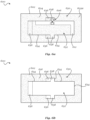
- Fig. 6a is a top plan view of inlay 600, illustrating the configuration of antenna structure 604, which is shown as the stippled area in the figure.
- Antenna structure 604 may be a continuous, unitary layer of conductive material and can be substantially coextensive with the first surface 603a of substrate 602, except for a gap 612 extending along a longitudinal edge of inner area 632 and a transverse edge of inner area 632.
- a strap or interposer 606 can bridge gap 612. In the illustrated embodiment, strap or interposer 606 can be disposed over a tab 638 and a portion of antenna structure 604 that is disposed over inner area 632.
- Fig. 6b is a bottom plan view of inlay 600, illustrating the configuration of ground plane 616, which is shown as the stippled area in the figure.
- Ground plane 616 may be a continuous, unitary layer of conductive material and can be substantially coextensive with only the outer area 630 of second surface 603b of substrate 602.
- inlay 600 may be substantially flat.
- a force may be applied to inner area 632.
- the hinges provided in substrate 602 can allow the inner area 632 to be vertically displaced from outer area 630.
- the inner area portion of antenna structure 604 consequently can act as a radiating element, while the outer area portion of antenna structure 604 is capacitively coupled to ground plane 616 and is conductively coupled to the radiating element.
- the vertical displacement of inner area 632 introduces a gap between the radiating element and the ground plane, thereby allowing air to act as a dielectric element for the inlay 600.
Landscapes
- Engineering & Computer Science (AREA)
- Computer Networks & Wireless Communication (AREA)
- Computer Hardware Design (AREA)
- Microelectronics & Electronic Packaging (AREA)
- Physics & Mathematics (AREA)
- General Physics & Mathematics (AREA)
- Theoretical Computer Science (AREA)
- Details Of Aerials (AREA)
- Structure Of Printed Boards (AREA)
- Shielding Devices Or Components To Electric Or Magnetic Fields (AREA)
Applications Claiming Priority (4)
| Application Number | Priority Date | Filing Date | Title |
|---|---|---|---|
| US13/798,557 US9172130B2 (en) | 2013-03-13 | 2013-03-13 | RFID inlay incorporating a ground plane |
| EP14719910.3A EP2973846B1 (de) | 2013-03-13 | 2014-03-11 | Rfid-einlage mit einer massefläche |
| EP19150354.9A EP3503289B1 (de) | 2013-03-13 | 2014-03-11 | Rfid-inlay mit einer massefläche |
| PCT/US2014/023593 WO2014164836A1 (en) | 2013-03-13 | 2014-03-11 | Rfid inlay incorporation a ground plane |
Related Parent Applications (3)
| Application Number | Title | Priority Date | Filing Date |
|---|---|---|---|
| EP19150354.9A Division EP3503289B1 (de) | 2013-03-13 | 2014-03-11 | Rfid-inlay mit einer massefläche |
| EP19150354.9A Division-Into EP3503289B1 (de) | 2013-03-13 | 2014-03-11 | Rfid-inlay mit einer massefläche |
| EP14719910.3A Division EP2973846B1 (de) | 2013-03-13 | 2014-03-11 | Rfid-einlage mit einer massefläche |
Publications (2)
| Publication Number | Publication Date |
|---|---|
| EP4498526A2 true EP4498526A2 (de) | 2025-01-29 |
| EP4498526A3 EP4498526A3 (de) | 2025-04-23 |
Family
ID=50588819
Family Applications (3)
| Application Number | Title | Priority Date | Filing Date |
|---|---|---|---|
| EP24217626.1A Pending EP4498526A3 (de) | 2013-03-13 | 2014-03-11 | Rfid-inlay mit einer massefläche |
| EP14719910.3A Active EP2973846B1 (de) | 2013-03-13 | 2014-03-11 | Rfid-einlage mit einer massefläche |
| EP19150354.9A Active EP3503289B1 (de) | 2013-03-13 | 2014-03-11 | Rfid-inlay mit einer massefläche |
Family Applications After (2)
| Application Number | Title | Priority Date | Filing Date |
|---|---|---|---|
| EP14719910.3A Active EP2973846B1 (de) | 2013-03-13 | 2014-03-11 | Rfid-einlage mit einer massefläche |
| EP19150354.9A Active EP3503289B1 (de) | 2013-03-13 | 2014-03-11 | Rfid-inlay mit einer massefläche |
Country Status (4)
| Country | Link |
|---|---|
| US (1) | US9172130B2 (de) |
| EP (3) | EP4498526A3 (de) |
| CN (1) | CN105229851B (de) |
| WO (1) | WO2014164836A1 (de) |
Families Citing this family (46)
| Publication number | Priority date | Publication date | Assignee | Title |
|---|---|---|---|---|
| US10518518B2 (en) | 2013-01-18 | 2019-12-31 | Féinics Amatech Teoranta | Smart cards with metal layer(s) and methods of manufacture |
| US10733494B2 (en) | 2014-08-10 | 2020-08-04 | Féinics Amatech Teoranta | Contactless metal card constructions |
| US10552722B2 (en) | 2014-08-10 | 2020-02-04 | Féinics Amatech Teoranta | Smartcard with coupling frame antenna |
| US10824931B2 (en) | 2012-08-30 | 2020-11-03 | Féinics Amatech Teoranta | Contactless smartcards with multiple coupling frames |
| US11551051B2 (en) | 2013-01-18 | 2023-01-10 | Amatech Group Limiied | Coupling frames for smartcards with various module opening shapes |
| US11341389B2 (en) | 2013-01-18 | 2022-05-24 | Amatech Group Limited | Manufacturing metal inlays for dual interface metal cards |
| US10977542B2 (en) | 2013-01-18 | 2021-04-13 | Amtech Group Limited Industrial Estate | Smart cards with metal layer(s) and methods of manufacture |
| US11928537B2 (en) | 2013-01-18 | 2024-03-12 | Amatech Group Limited | Manufacturing metal inlays for dual interface metal cards |
| US11354558B2 (en) | 2013-01-18 | 2022-06-07 | Amatech Group Limited | Contactless smartcards with coupling frames |
| US11354560B2 (en) | 2013-01-18 | 2022-06-07 | Amatech Group Limited | Smartcards with multiple coupling frames |
| US10599972B2 (en) | 2013-01-18 | 2020-03-24 | Féinics Amatech Teoranta | Smartcard constructions and methods |
| US10929835B2 (en) | 2013-08-13 | 2021-02-23 | Neology, Inc. | Detachable radio frequency identification switch tag |
| US10678382B2 (en) | 2014-04-22 | 2020-06-09 | Avery Dennison Retail Information Services, Llc | Methods and systems for monitoring medication compliance |
| WO2016046184A1 (en) * | 2014-09-22 | 2016-03-31 | Féinics Amatech Teoranta | Passive smart cards, metal cards, payment objects and smart jewelry |
| US10762753B2 (en) | 2014-12-12 | 2020-09-01 | Avery Dennison Retail Information Services, Llc | Methods and systems for determining the time at which a seal was broken |
| US11403506B2 (en) | 2015-05-21 | 2022-08-02 | Neology, Inc. | Detachable radio frequency identification switch tag |
| US10913594B2 (en) | 2015-07-07 | 2021-02-09 | Avery Dennison Retail Information Services, Llc | Smart ejection trays for use with medication containers |
| US10896301B2 (en) | 2015-07-07 | 2021-01-19 | Avery Dennison Retail Information Services, Llc | RFID-based methods and systems for monitoring medication compliance |
| DE212016000146U1 (de) * | 2015-07-21 | 2018-03-12 | Murata Manufacturing Co., Ltd. | Drahtloskommunikationsbauelement und mit demselben ausgestatteter Artikel |
| US10320053B2 (en) * | 2016-02-16 | 2019-06-11 | GM Global Technology Operations LLC | Wideband coplanar waveguide fed monopole applique antennas |
| US20180012117A1 (en) * | 2016-07-07 | 2018-01-11 | Avery Dennison Retail Information Services, Llc | Medication containers incorporating wireless communication devices and methods for manufacturing such containers |
| WO2018034449A1 (ko) * | 2016-08-17 | 2018-02-22 | 주식회사 아이씨케이 | 비접촉식 카드 기능을 갖는 메탈 카드 및 그에 사용되는 금속판과 금속판 조립체, 그리고 그 제조 방법 |
| WO2018045550A1 (en) * | 2016-09-09 | 2018-03-15 | Hong Kong R&D Centre for Logistics and Supply Chain Management Enabling Technologies Limited | A radio frequency communication device and a method for using thereof |
| US10121100B2 (en) * | 2016-12-20 | 2018-11-06 | Capital One Services, Llc | Two piece transaction card having fabric inlay |
| US9922277B1 (en) * | 2017-02-16 | 2018-03-20 | Jesse James Hess | Barrier for concealing text of a transactional card |
| USD840981S1 (en) * | 2017-10-20 | 2019-02-19 | Avery Dennison Retail Information Services, Llc | RFID inlay |
| USD840982S1 (en) * | 2017-10-20 | 2019-02-19 | Avery Dennison Retail Information Services, Llc | RFID inlay |
| USD856985S1 (en) * | 2017-10-20 | 2019-08-20 | Avery Dennison Retail Information Services, Llc | RFID inlay |
| WO2019224575A1 (en) | 2018-05-22 | 2019-11-28 | Tyco Fire & Security Gmbh | Elongate flexible tag |
| EP3583842B1 (de) | 2018-06-18 | 2022-02-16 | Assa Abloy AB | Rfid-etikett |
| WO2020047460A1 (en) * | 2018-08-30 | 2020-03-05 | Avery Dennison Retail Information Services, Llc | Method, system, and apparatus for broadband and multi-frequency antennas for rfid devices formed by folding a planar structure |
| EP3877910A4 (de) | 2018-11-07 | 2022-08-03 | Neology, Inc. | Entfernbares funkfrequenzidentifizierungsschalteretikett |
| CN211033618U (zh) * | 2019-07-19 | 2020-07-17 | 鼎贞(厦门)实业有限公司 | 一种密封瓶口的射频识别垫片 |
| US12223814B2 (en) | 2019-09-16 | 2025-02-11 | Sensormatic Electronics, LLC | Security tag for textiles using conductive thread |
| US10970613B1 (en) | 2019-09-18 | 2021-04-06 | Sensormatic Electronics, LLC | Systems and methods for providing tags adapted to be incorporated with or in items |
| US11443160B2 (en) | 2019-09-18 | 2022-09-13 | Sensormatic Electronics, LLC | Systems and methods for laser tuning and attaching RFID tags to products |
| US11055588B2 (en) | 2019-11-27 | 2021-07-06 | Sensormatic Electronics, LLC | Flexible water-resistant sensor tag |
| US12524640B2 (en) | 2019-11-27 | 2026-01-13 | Sensormatic Electronics, LLC | Flexible water-resistant sensor tag |
| WO2022126618A1 (en) * | 2020-12-18 | 2022-06-23 | Confidex Oy | Rfid tag |
| US11755874B2 (en) | 2021-03-03 | 2023-09-12 | Sensormatic Electronics, LLC | Methods and systems for heat applied sensor tag |
| US11916311B2 (en) | 2021-04-30 | 2024-02-27 | Apple Inc. | Electronic devices having folded antenna modules |
| US11869324B2 (en) | 2021-12-23 | 2024-01-09 | Sensormatic Electronics, LLC | Securing a security tag into an article |
| USD1082761S1 (en) * | 2023-10-20 | 2025-07-08 | Avery Dennison Retail Information Services Llc | Antenna |
| WO2026030274A1 (en) * | 2024-07-29 | 2026-02-05 | Avery Dennison Retail Information Services Llc | Rfid device, systems, and methods of manufacturing thereof with enhanced environmental performance |
| WO2026043592A1 (en) * | 2024-08-19 | 2026-02-26 | Sensormatic Electronics, LLC | Multi-layer radio frequency identification label and method of making same |
| WO2026064617A1 (en) * | 2024-09-20 | 2026-03-26 | Hid Global Corp. | Rfid integration into an adaptable substrate assembly |
Family Cites Families (28)
| Publication number | Priority date | Publication date | Assignee | Title |
|---|---|---|---|---|
| US6049314A (en) | 1998-11-17 | 2000-04-11 | Xertex Technologies, Inc. | Wide band antenna having unitary radiator/ground plane |
| US6693541B2 (en) * | 2001-07-19 | 2004-02-17 | 3M Innovative Properties Co | RFID tag with bridge circuit assembly and methods of use |
| DE10204884A1 (de) | 2002-02-06 | 2003-08-14 | Schreiner Gmbh & Co Kg | Transponderetikett |
| US7501984B2 (en) * | 2003-11-04 | 2009-03-10 | Avery Dennison Corporation | RFID tag using a surface insensitive antenna structure |
| JP4204371B2 (ja) * | 2003-04-17 | 2009-01-07 | トッパン・フォームズ株式会社 | Rf−idメディアの製造方法 |
| US7336243B2 (en) * | 2003-05-29 | 2008-02-26 | Sky Cross, Inc. | Radio frequency identification tag |
| CA2544736A1 (en) | 2003-11-04 | 2005-05-19 | Avery Dennison Corporation | Rfid tag with enhanced readability |
| US7573390B2 (en) | 2004-03-15 | 2009-08-11 | Iwata Label Co., Ltd. | Split-able label |
| GB0501199D0 (en) * | 2005-01-21 | 2005-03-02 | Qinetiq Ltd | Improved RF tags |
| KR100983571B1 (ko) | 2005-06-16 | 2010-09-24 | 후지쯔 가부시끼가이샤 | 태그 안테나 및 rfid 태그 |
| US7408512B1 (en) * | 2005-10-05 | 2008-08-05 | Sandie Corporation | Antenna with distributed strip and integrated electronic components |
| ES2395856T3 (es) * | 2006-07-24 | 2013-02-15 | Textilma Ag | Etiqueta RFID |
| DE102006052517A1 (de) * | 2006-11-06 | 2008-05-08 | Bielomatik Leuze Gmbh + Co.Kg | Chipmodul für ein RFID-System |
| JP4950627B2 (ja) * | 2006-11-10 | 2012-06-13 | 株式会社日立製作所 | Rficタグとその使用方法 |
| US20080122631A1 (en) * | 2006-11-29 | 2008-05-29 | Intermec Ip Corp. | Multiple band / wide band radio frequency identification (rfid) tag, such as for use as a metal mount tag |
| US20090051614A1 (en) | 2007-08-20 | 2009-02-26 | Hang Wong | Folded dipole antenna |
| TWI355610B (en) | 2007-12-21 | 2012-01-01 | Ind Tech Res Inst | Anti-metal rf identification tag and the manufactu |
| EP2182471A1 (de) | 2008-11-03 | 2010-05-05 | Schreiner Group GmbH & Co. KG | Transponderetikett auf einer Metallfläche und Verfahren zum Anordnen eines Transponderetiketts auf einer Metallfläche |
| US8424176B2 (en) * | 2008-11-25 | 2013-04-23 | Kovio, Inc. | Methods of forming tunable capacitors |
| CN101777137A (zh) * | 2009-01-08 | 2010-07-14 | 中国钢铁股份有限公司 | 利用单极天线的无线射频辨识系统标签 |
| US8833664B2 (en) | 2009-12-18 | 2014-09-16 | Yu Yung Choi | Enhanced performance and security RFID device |
| JP5170156B2 (ja) * | 2010-05-14 | 2013-03-27 | 株式会社村田製作所 | 無線icデバイス |
| JP5456598B2 (ja) | 2010-06-25 | 2014-04-02 | 富士通株式会社 | 無線タグ、及びその製造方法 |
| KR101050241B1 (ko) * | 2010-09-27 | 2011-07-19 | 충남대학교산학협력단 | 알에프아이디 금속태그용 비대칭 평면 다이폴 안테나 |
| TW201236927A (en) * | 2011-03-11 | 2012-09-16 | China Steel Corp | Anti-counterfeiting bottle |
| US8917214B2 (en) | 2011-03-16 | 2014-12-23 | Avery Dennison Corporation | Dual band RFID device and method of formulation |
| DE102011104170A1 (de) | 2011-06-14 | 2012-12-20 | Schreiner Group Gmbh & Co. Kg | Transponderetikett und Herstellungsverfahren für ein Transponderetikett |
| US8985467B2 (en) * | 2012-02-01 | 2015-03-24 | Checkpoint Systems, Inc. | Permanently deactivatable security tag |
-
2013
- 2013-03-13 US US13/798,557 patent/US9172130B2/en active Active
-
2014
- 2014-03-11 EP EP24217626.1A patent/EP4498526A3/de active Pending
- 2014-03-11 CN CN201480027338.4A patent/CN105229851B/zh active Active
- 2014-03-11 EP EP14719910.3A patent/EP2973846B1/de active Active
- 2014-03-11 EP EP19150354.9A patent/EP3503289B1/de active Active
- 2014-03-11 WO PCT/US2014/023593 patent/WO2014164836A1/en not_active Ceased
Also Published As
| Publication number | Publication date |
|---|---|
| CN105229851B (zh) | 2021-10-08 |
| EP4498526A3 (de) | 2025-04-23 |
| EP3503289B1 (de) | 2025-01-22 |
| EP3503289A2 (de) | 2019-06-26 |
| EP3503289A3 (de) | 2019-08-14 |
| US20140263655A1 (en) | 2014-09-18 |
| WO2014164836A1 (en) | 2014-10-09 |
| US9172130B2 (en) | 2015-10-27 |
| EP2973846B1 (de) | 2019-01-09 |
| CN105229851A (zh) | 2016-01-06 |
| EP2973846A1 (de) | 2016-01-20 |
Similar Documents
| Publication | Publication Date | Title |
|---|---|---|
| EP3503289B1 (de) | Rfid-inlay mit einer massefläche | |
| CN101142711B (zh) | 适用于金属的rfid标签及其rfid标签部 | |
| KR100979874B1 (ko) | 트랜스폰더를 포함하는 라벨 및 트랜스폰더를 포함하는시스템 | |
| US7501984B2 (en) | RFID tag using a surface insensitive antenna structure | |
| EP2309589B1 (de) | Rfid-etikett mit einer flächenunempfindlichen antennenstruktur | |
| CN101292272B (zh) | 带有电子元件的标签及其制作方法 | |
| EP1758050B1 (de) | RFID-Etikett und Herstellungsverfahren dafür | |
| US7598867B2 (en) | Techniques for folded tag antennas | |
| EP2960834B1 (de) | Behälter | |
| US20100265041A1 (en) | Rfid transponder | |
| EP3001394B1 (de) | Verfahren zur herstellung eines kombinationsdiebstahlsicherungs- und verfolgungsetiketts | |
| US11100378B2 (en) | Packaging paperboard and method for manufacturing same | |
| JP2022509069A (ja) | Rfidラベルの形成及び配置のための方法、システム並びに装置 | |
| JP7613861B2 (ja) | Rfidラベル及びrfidラベルの使用方法 | |
| KR20160030554A (ko) | 무선 ic 태그 부착 패키지 및 무선 ic 태그 부착 패키지의 제조 방법 | |
| JP2005196377A (ja) | Rfidタグラベル | |
| EP1620916B1 (de) | Hfid-etikett mit einer oberflächenunempfindlichen antennenstruktur | |
| EP2410604B1 (de) | UHF-RFID-Antenne und Anpassungsnetzwerk in eine Einweg-Metall-Deckel integriert | |
| JP2022029374A (ja) | Rfタグ付き物品およびrfタグ付き物品の載置方法 | |
| EP2225707B1 (de) | Verfahren zur herstellung einer antenne oder einer schlaufe auf einem substrat zur aufnahme einer integrierten schaltung |
Legal Events
| Date | Code | Title | Description |
|---|---|---|---|
| PUAI | Public reference made under article 153(3) epc to a published international application that has entered the european phase |
Free format text: ORIGINAL CODE: 0009012 |
|
| STAA | Information on the status of an ep patent application or granted ep patent |
Free format text: STATUS: THE APPLICATION HAS BEEN PUBLISHED |
|
| AC | Divisional application: reference to earlier application |
Ref document number: 2973846 Country of ref document: EP Kind code of ref document: P Ref document number: 3503289 Country of ref document: EP Kind code of ref document: P |
|
| AK | Designated contracting states |
Kind code of ref document: A2 Designated state(s): AL AT BE BG CH CY CZ DE DK EE ES FI FR GB GR HR HU IE IS IT LI LT LU LV MC MK MT NL NO PL PT RO RS SE SI SK SM TR |
|
| REG | Reference to a national code |
Ref country code: DE Ref legal event code: R079 Free format text: PREVIOUS MAIN CLASS: H01Q0009400000 Ipc: H01Q0001220000 |
|
| PUAL | Search report despatched |
Free format text: ORIGINAL CODE: 0009013 |
|
| AK | Designated contracting states |
Kind code of ref document: A3 Designated state(s): AL AT BE BG CH CY CZ DE DK EE ES FI FR GB GR HR HU IE IS IT LI LT LU LV MC MK MT NL NO PL PT RO RS SE SI SK SM TR |
|
| RIC1 | Information provided on ipc code assigned before grant |
Ipc: H01Q 1/38 20060101ALI20250317BHEP Ipc: H01Q 9/40 20060101ALI20250317BHEP Ipc: H01Q 1/08 20060101ALI20250317BHEP Ipc: G06K 19/077 20060101ALI20250317BHEP Ipc: H01Q 1/22 20060101AFI20250317BHEP |
|
| STAA | Information on the status of an ep patent application or granted ep patent |
Free format text: STATUS: REQUEST FOR EXAMINATION WAS MADE |
|
| 17P | Request for examination filed |
Effective date: 20251016 |
|
| GRAP | Despatch of communication of intention to grant a patent |
Free format text: ORIGINAL CODE: EPIDOSNIGR1 |
|
| STAA | Information on the status of an ep patent application or granted ep patent |
Free format text: STATUS: GRANT OF PATENT IS INTENDED |
|
| INTG | Intention to grant announced |
Effective date: 20260220 |