EP4495984A1 - Verfahren zur herstellung einer verbindungsdurchkontaktierung - Google Patents
Verfahren zur herstellung einer verbindungsdurchkontaktierung Download PDFInfo
- Publication number
- EP4495984A1 EP4495984A1 EP23186608.8A EP23186608A EP4495984A1 EP 4495984 A1 EP4495984 A1 EP 4495984A1 EP 23186608 A EP23186608 A EP 23186608A EP 4495984 A1 EP4495984 A1 EP 4495984A1
- Authority
- EP
- European Patent Office
- Prior art keywords
- layer
- conductive
- line
- dielectric
- hardmask
- Prior art date
- Legal status (The legal status is an assumption and is not a legal conclusion. Google has not performed a legal analysis and makes no representation as to the accuracy of the status listed.)
- Pending
Links
Images


Classifications
-
- H—ELECTRICITY
- H10—SEMICONDUCTOR DEVICES; ELECTRIC SOLID-STATE DEVICES NOT OTHERWISE PROVIDED FOR
- H10W—GENERIC PACKAGES, INTERCONNECTIONS, CONNECTORS OR OTHER CONSTRUCTIONAL DETAILS OF DEVICES COVERED BY CLASS H10
- H10W20/00—Interconnections in chips, wafers or substrates
- H10W20/01—Manufacture or treatment
- H10W20/031—Manufacture or treatment of conductive parts of the interconnections
- H10W20/0698—Local interconnections
-
- H—ELECTRICITY
- H10—SEMICONDUCTOR DEVICES; ELECTRIC SOLID-STATE DEVICES NOT OTHERWISE PROVIDED FOR
- H10W—GENERIC PACKAGES, INTERCONNECTIONS, CONNECTORS OR OTHER CONSTRUCTIONAL DETAILS OF DEVICES COVERED BY CLASS H10
- H10W10/00—Isolation regions in semiconductor bodies between components of integrated devices
- H10W10/01—Manufacture or treatment
- H10W10/021—Manufacture or treatment of air gaps
-
- H—ELECTRICITY
- H10—SEMICONDUCTOR DEVICES; ELECTRIC SOLID-STATE DEVICES NOT OTHERWISE PROVIDED FOR
- H10W—GENERIC PACKAGES, INTERCONNECTIONS, CONNECTORS OR OTHER CONSTRUCTIONAL DETAILS OF DEVICES COVERED BY CLASS H10
- H10W10/00—Isolation regions in semiconductor bodies between components of integrated devices
- H10W10/20—Air gaps
-
- H—ELECTRICITY
- H10—SEMICONDUCTOR DEVICES; ELECTRIC SOLID-STATE DEVICES NOT OTHERWISE PROVIDED FOR
- H10W—GENERIC PACKAGES, INTERCONNECTIONS, CONNECTORS OR OTHER CONSTRUCTIONAL DETAILS OF DEVICES COVERED BY CLASS H10
- H10W20/00—Interconnections in chips, wafers or substrates
- H10W20/01—Manufacture or treatment
- H10W20/021—Manufacture or treatment of interconnections within wafers or substrates
- H10W20/023—Manufacture or treatment of interconnections within wafers or substrates the interconnections being through-semiconductor vias
-
- H—ELECTRICITY
- H10—SEMICONDUCTOR DEVICES; ELECTRIC SOLID-STATE DEVICES NOT OTHERWISE PROVIDED FOR
- H10W—GENERIC PACKAGES, INTERCONNECTIONS, CONNECTORS OR OTHER CONSTRUCTIONAL DETAILS OF DEVICES COVERED BY CLASS H10
- H10W20/00—Interconnections in chips, wafers or substrates
- H10W20/01—Manufacture or treatment
- H10W20/031—Manufacture or treatment of conductive parts of the interconnections
- H10W20/056—Manufacture or treatment of conductive parts of the interconnections by filling conductive material into holes, grooves or trenches
-
- H—ELECTRICITY
- H10—SEMICONDUCTOR DEVICES; ELECTRIC SOLID-STATE DEVICES NOT OTHERWISE PROVIDED FOR
- H10W—GENERIC PACKAGES, INTERCONNECTIONS, CONNECTORS OR OTHER CONSTRUCTIONAL DETAILS OF DEVICES COVERED BY CLASS H10
- H10W20/00—Interconnections in chips, wafers or substrates
- H10W20/01—Manufacture or treatment
- H10W20/031—Manufacture or treatment of conductive parts of the interconnections
- H10W20/063—Manufacture or treatment of conductive parts of the interconnections by forming conductive members before forming protective insulating material
-
- H—ELECTRICITY
- H10—SEMICONDUCTOR DEVICES; ELECTRIC SOLID-STATE DEVICES NOT OTHERWISE PROVIDED FOR
- H10W—GENERIC PACKAGES, INTERCONNECTIONS, CONNECTORS OR OTHER CONSTRUCTIONAL DETAILS OF DEVICES COVERED BY CLASS H10
- H10W20/00—Interconnections in chips, wafers or substrates
- H10W20/01—Manufacture or treatment
- H10W20/031—Manufacture or treatment of conductive parts of the interconnections
- H10W20/063—Manufacture or treatment of conductive parts of the interconnections by forming conductive members before forming protective insulating material
- H10W20/0633—Manufacture or treatment of conductive parts of the interconnections by forming conductive members before forming protective insulating material using subtractive patterning of the conductive members
-
- H—ELECTRICITY
- H10—SEMICONDUCTOR DEVICES; ELECTRIC SOLID-STATE DEVICES NOT OTHERWISE PROVIDED FOR
- H10W—GENERIC PACKAGES, INTERCONNECTIONS, CONNECTORS OR OTHER CONSTRUCTIONAL DETAILS OF DEVICES COVERED BY CLASS H10
- H10W20/00—Interconnections in chips, wafers or substrates
- H10W20/01—Manufacture or treatment
- H10W20/031—Manufacture or treatment of conductive parts of the interconnections
- H10W20/069—Manufacture or treatment of conductive parts of the interconnections by forming self-aligned vias or self-aligned contact plugs
-
- H—ELECTRICITY
- H10—SEMICONDUCTOR DEVICES; ELECTRIC SOLID-STATE DEVICES NOT OTHERWISE PROVIDED FOR
- H10W—GENERIC PACKAGES, INTERCONNECTIONS, CONNECTORS OR OTHER CONSTRUCTIONAL DETAILS OF DEVICES COVERED BY CLASS H10
- H10W20/00—Interconnections in chips, wafers or substrates
- H10W20/01—Manufacture or treatment
- H10W20/031—Manufacture or treatment of conductive parts of the interconnections
- H10W20/069—Manufacture or treatment of conductive parts of the interconnections by forming self-aligned vias or self-aligned contact plugs
- H10W20/0693—Manufacture or treatment of conductive parts of the interconnections by forming self-aligned vias or self-aligned contact plugs by forming self-aligned vias
-
- H—ELECTRICITY
- H10—SEMICONDUCTOR DEVICES; ELECTRIC SOLID-STATE DEVICES NOT OTHERWISE PROVIDED FOR
- H10W—GENERIC PACKAGES, INTERCONNECTIONS, CONNECTORS OR OTHER CONSTRUCTIONAL DETAILS OF DEVICES COVERED BY CLASS H10
- H10W20/00—Interconnections in chips, wafers or substrates
- H10W20/01—Manufacture or treatment
- H10W20/071—Manufacture or treatment of dielectric parts thereof
- H10W20/072—Manufacture or treatment of dielectric parts thereof of dielectric parts comprising air gaps
-
- H—ELECTRICITY
- H10—SEMICONDUCTOR DEVICES; ELECTRIC SOLID-STATE DEVICES NOT OTHERWISE PROVIDED FOR
- H10W—GENERIC PACKAGES, INTERCONNECTIONS, CONNECTORS OR OTHER CONSTRUCTIONAL DETAILS OF DEVICES COVERED BY CLASS H10
- H10W20/00—Interconnections in chips, wafers or substrates
- H10W20/01—Manufacture or treatment
- H10W20/071—Manufacture or treatment of dielectric parts thereof
- H10W20/081—Manufacture or treatment of dielectric parts thereof by forming openings in the dielectric parts
-
- H—ELECTRICITY
- H10—SEMICONDUCTOR DEVICES; ELECTRIC SOLID-STATE DEVICES NOT OTHERWISE PROVIDED FOR
- H10W—GENERIC PACKAGES, INTERCONNECTIONS, CONNECTORS OR OTHER CONSTRUCTIONAL DETAILS OF DEVICES COVERED BY CLASS H10
- H10W20/00—Interconnections in chips, wafers or substrates
- H10W20/01—Manufacture or treatment
- H10W20/071—Manufacture or treatment of dielectric parts thereof
- H10W20/092—Manufacture or treatment of dielectric parts thereof by smoothing the dielectric parts
-
- H—ELECTRICITY
- H10—SEMICONDUCTOR DEVICES; ELECTRIC SOLID-STATE DEVICES NOT OTHERWISE PROVIDED FOR
- H10W—GENERIC PACKAGES, INTERCONNECTIONS, CONNECTORS OR OTHER CONSTRUCTIONAL DETAILS OF DEVICES COVERED BY CLASS H10
- H10W20/00—Interconnections in chips, wafers or substrates
- H10W20/40—Interconnections external to wafers or substrates, e.g. back-end-of-line [BEOL] metallisations or vias connecting to gate electrodes
- H10W20/41—Interconnections external to wafers or substrates, e.g. back-end-of-line [BEOL] metallisations or vias connecting to gate electrodes characterised by their conductive parts
- H10W20/42—Vias, e.g. via plugs
-
- H—ELECTRICITY
- H10—SEMICONDUCTOR DEVICES; ELECTRIC SOLID-STATE DEVICES NOT OTHERWISE PROVIDED FOR
- H10W—GENERIC PACKAGES, INTERCONNECTIONS, CONNECTORS OR OTHER CONSTRUCTIONAL DETAILS OF DEVICES COVERED BY CLASS H10
- H10W20/00—Interconnections in chips, wafers or substrates
- H10W20/40—Interconnections external to wafers or substrates, e.g. back-end-of-line [BEOL] metallisations or vias connecting to gate electrodes
- H10W20/45—Interconnections external to wafers or substrates, e.g. back-end-of-line [BEOL] metallisations or vias connecting to gate electrodes characterised by their insulating parts
- H10W20/46—Interconnections external to wafers or substrates, e.g. back-end-of-line [BEOL] metallisations or vias connecting to gate electrodes characterised by their insulating parts comprising air gaps
-
- H—ELECTRICITY
- H10—SEMICONDUCTOR DEVICES; ELECTRIC SOLID-STATE DEVICES NOT OTHERWISE PROVIDED FOR
- H10W—GENERIC PACKAGES, INTERCONNECTIONS, CONNECTORS OR OTHER CONSTRUCTIONAL DETAILS OF DEVICES COVERED BY CLASS H10
- H10W20/00—Interconnections in chips, wafers or substrates
- H10W20/40—Interconnections external to wafers or substrates, e.g. back-end-of-line [BEOL] metallisations or vias connecting to gate electrodes
- H10W20/495—Capacitive arrangements or effects of, or between wiring layers
Definitions
- the present invention is related to semiconductor processing, in particular to the formation of interconnect vias between two levels of conductors of a multi-level interconnect structure of a semiconductor chip.
- Multilayer conductive structures are typically built as layers of conductive lines, with interconnect vias formed between lines of the respective layers.
- interconnect vias formed between lines of the respective layers.
- traditional lithography and etch processes are no longer able to ensure acceptable alignment between an interconnect via and the underlying line to which the via is connected.
- Patent publication document US2017256451 discloses a method wherein the metal lines of the lower level are formed by a patterning step using a hardmask in the form of a line array, and wherein the hardmask lines are maintained on the metal lines except at the via locations. At these locations, the hardmask is locally removed by lithography and selective etching to create a self-aligned via opening, which is subsequently filled by a damascene-type metal fill process.
- the hardmask lines are however reduced in size and/or oxidized after the metal line patterning, which can make it difficult to produce the via opening, especially at the deepest levels of a multi-level interconnect structure where the in-plane dimensions of the via opening may be in the order of a few nanometres.
- the remaining hardmask material is likely to increase the interlayer capacitance so there is an interest in using a hardmask material having low relative permittivity.
- the invention aims to provide a solution to the problems indicated hereabove. This aim is achieved by a method according to the appended claims.
- the invention is thus related to a method for producing an interconnect via for connecting a lower conductive line to an upper conductive line overlying the lower line.
- 'conductive' is intended to refer to 'electrically conductive'.
- the method is especially useful for the formation of interconnect vias which are nano-sized in three orthogonal directions, i.e. in terms of their width, length and height.
- the term 'nano-sized' in the present context is to be understood as: having at least one dimension of a few nanometres up to a few tens of nanometres.
- a nano-sized conductive line is a line having a nano-sized width and height.
- a nano-sized interconnect via is a via having a nano-sized width, length and height.
- a conductive layer is produced on a substrate having an upper surface formed of a dielectric material with electrical conductors or contacts embedded in said dielectric material.
- the substrate may for example be a process wafer whereon a FEOL portion and one or more layers of a BEOL portion have been produced according to a given layout for a number of integrated circuits arranged on the wafer.
- a dielectric layer is then produced on the conductive layer.
- An opening is formed in the dielectric layer and subsequently filled with a conductive material, after which the conductive material is planarized to the level of the dielectric material so that a conductive via is formed in the opening.
- the dielectric material, the conductive material of the via, and of the conductive layer are then removed in the areas not covered by the hardmask line, resulting in a conductive line, having an interconnect via on its top surface.
- the interconnect via is formed by the removal of said shoulders of the original via, so that the interconnect via is aligned to the width of the conductive line.
- a second dielectric material is then produced and planarized to the top level of the hardmask line.
- the hardmask line and an upper portion of the second dielectric material are then removed (simultaneously or consecutively) so that a planar dielectric surface is produced with the top of the interconnect via coplanar therewith.
- the conductive lines of the next level of the interconnect structure can be formed on the planar surface.
- a set of parallel conductive lines is formed with several self-aligned interconnect vias on one or more of said lines, said interconnect vias being produced in accordance with the method of the invention.
- said second dielectric material is deposited in the spaces between the lines. According to preferred embodiments, this is done in such a manner that airgaps are formed between adjacent lines.
- the method of the invention differs from existing methods by the specific order of the steps: etching of the conductive lines of the lower level is done after the formation of an initial via on top of a blanket conductive layer.
- the initial via obtained by filling the opening becomes the interconnect via which is therefore self-aligned to the width of the underlying conductive line.
- the formation (including etching and cleaning steps) and filling of the opening for producing the initial via is easier because the width of the opening in the direction perpendicular to the conductive line is larger than said line width. This results in good via to underlying conductive line contact formation and thus, lower across-wafer nonuniformity, lower via resistance and superior reliability properties.
- interlayer capacitance of the resulting multilevel interconnect structure is that the hardmask lines are removed after the formation of the interconnect via.
- inter-line airgaps can be extended to the level of the interconnect via thus providing significant further improvement in terms of capacitance.
- the invention is in particular related to a method for producing an interconnect via for connecting a lower electrically conductive line in a first level of a multi-level interconnect structure to an upper electrically conductive line in a second level overlying said first level.
- first level and second level refer to any two consecutive levels of the interconnect structure. The method comprises the steps of:
- the hardmask line is one of an array of parallel lines.
- the second dielectric material is deposited in such a manner that airgaps are created between adjacent conductive lines.
- an airgap is formed on each side of the conductive line on top of which the interconnect via is formed, and said two airgaps have a top portion that overlaps a lower portion of the height of the interconnect via.
- the height (H1) of said top portion of the two airgaps is at least 50% of the height of the interconnect via.
- the interconnect via has nano-sized dimensions in three orthogonal directions.
- the height of the interconnect via is between 10 nm and 30 nm.
- the opening is filled by a bottom-up fill technique and wherein the step of planarizing the surface of the dielectric layer is done without a CMP (chemical mechanical polishing) step.
- CMP chemical mechanical polishing
- the first and second conductive material are chosen from the group consisting of Ru, W and Mo.
- the first and second dielectric material is SiO 2 or a low-K material.
- an adhesion layer is produced on the substrate prior to forming the layer of the first conductive material, and/or wherein an adhesion layer is produced on the layer of the first conductive material, prior to forming the dielectric layer.
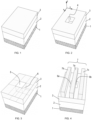
- Figure 1 shows a small section of a substrate comprising a base portion 1 which may be a nano-sized upper slice of a silicon process wafer after the front end of line (FEOL) processing and part of the back end of line (BEOL) processing.
- FEOL front end of line
- BEOL back end of line
- the FEOL process constitutes a sequence of processing steps for producing large numbers of semiconductor devices such as transistors and diodes on usually a silicon wafer, according to the layout of several integrated circuit chips.
- BEOL processing adds a multi-level interconnect structure on top of the FEOL portion of the chips, said interconnect structure comprising multiple levels of electrically conductive lines, interconnected according to a predefined interconnection scheme by vertical interconnects, referred to in the present description as 'interconnect vias'.
- the interconnect levels are usually labelled Metal0, Metal1, Metal2, etc (in short M0, M1, M2, etc), as the line material is usually a metal such as Cu, W or Ru.
- the deepest level M0 includes connections in direct contact with the active devices in the FEOL and is also referred to as the Middle of Line portion (MOL) of an integrated circuit.
- MOL Middle of Line portion
- the top surface of the base portion 1 is formed of a dielectric material, for example SiO 2 or low-K dielectric onto which surface the conductive lines of an interconnect level Mi are to be formed.
- a dielectric material for example SiO 2 or low-K dielectric onto which surface the conductive lines of an interconnect level Mi are to be formed.
- electrical conductors or contacts embedded in said dielectric layer are electrical conductors or contacts, which may include conductive lines in level Mi-1 or interconnect vias intended to connect the lines of level Mx to the lines of level Mi-1, or connections to source or drain electrodes of transistors of the FEOL portion if level Mi-1 is the M0 level (MOL).
- the first layer 2 is a conductive layer.
- this may for example be a layer of Ru, W or Mo.
- an adhesion layer such as a thin TiN layer between the base substrate 1 and the Ru layer 2.
- a layer 3 of dielectric material for example SiO 2 or a low-K dielectric, is deposited.
- An adhesion layer may again be required between the conductive layer 2 and the dielectric layer 3, depending on the material of layer 2. The exemplary case is shown however wherein no adhesion layers are applied.
- the thickness of the various layers depends on the metallization levels to which the method is applied, i.e. the value of i.
- the method of the invention is applicable down to the deepest levels and provides the most benefits at these levels given the importance of controlling the via alignment at the nano-sized dimensions applicable at these deep levels.
- the thickness of layer 2 may be in the order of 25 nm while the thickness of layer 3 may be in the order of 15 nm.
- an opening 4 is now formed in the dielectric layer 3.
- the opening 4 is a cavity that is open to the surface of the dielectric layer 3.
- the opening 4 is represented as having a rectangular cross-section, but the opening may be shaped differently, for example having an ellipse-shaped or circular cross-section.
- the lateral dimensions of the opening may for example be in the order of 18 nm in the x-direction and y-direction, with reference to the orthogonal axes included in Figure 2 .
- a known way of producing openings of these dimensions is to a apply a hardmask formed of a stack of SOC (spin-on-carbon), SOG (spin-on-glass) and photoresist.
- the photoresist is patterned to form openings which are larger than the targeted dimensions and shrink technology is applied to arrive at the desired dimensions of the opening 4.
- shrink technology is known as such and details thereof are not required here.
- a more straightforward lithography and etch process may be used as the lateral dimensions of the opening will be larger at those levels.
- the bottom of the opening 4 is formed of the conductive material of layer 2. Therefore, if an adhesion layer is present between layer 2 and layer 3, the adhesion layer needs to be removed selectively with respect to the material of layer 2.
- the opening 4 is then filled with a second conductive material, which may or may not be the same as the conductive material of layer 2.
- a second conductive material which may or may not be the same as the conductive material of layer 2.
- An additional conductive adhesion liner on the bottom of the opening 4 may be required before the opening is filled with the second material.
- Filling the opening 4 may be done by a known technique such as CVD (Chemical Vapour Deposition) or ALD (Atomic Layer Deposition), which will result in a thick layer of the second conductive material on top of the dielectric layer 3.
- This layer is then removed by grinding and CMP (chemical mechanical polishing), until a planarized surface is obtained as shown in Figure 3 : the planarized surface is formed of the dielectric material of layer 3, with an island 5 of conductive material coplanar therewith.
- the island 5 forms the top surface of a via 6 of conductive material that is in electrical contact with the underlying conductive layer 2.
- the via 6 is represented in Figure 3 with the help of a number of auxiliary lines which help to visualize the position of the via relative to layers 2 and 3.
- Another way of filling the opening 4 is by a bottom-up fill technique (known as such) wherein the via 6 is built up from the bottom of the opening 4 and the via material is not deposited on the dielectric layer 3 until the opening is filled.
- a hardmask layer is then produced on the planarized surface and patterned according to a regular pattern of parallel lines 7 oriented in the x-direction and having essentially the same width and height.
- one line 7a is overlapping the via 6, so that lateral shoulders 6a and 6bof the via 6 extend on both sides of said line 7a without overlapping the adjacent lines 7b and 7c.
- the lithography and etch steps applied for producing the lines 7 are configured to produce the line 7a concentrically with respect to said y-dimension of the via 6.
- an unavoidable overlay error of 1 or 2 nm may result in a slight deviation of this theoretical case.
- the lines 7 are formed in such a way that two shoulders 6a and 6b of the conductive via 6 are exposed on both sides of the hardmask line 7a.
- etch steps are performed for transferring the hardmask line pattern to the underlying layers.
- the images shown in Figures 5 and 6 illustrate a 2-step process but depending on the applied materials and dimensions, a single step process may also be applicable.
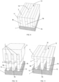
- the dielectric layer 3 is removed selectively with respect to the conductive via 6, in the areas not covered by the hardmask lines 7, resulting in dielectric lines 3 on the conductive layer 2, and the exposure of the shoulders 6a and 6b of the via 6.
- a second etch step illustrated in Figure 6 the conductive materials of the via 6 and of the underlying layer 2 are etched in the areas not covered by the hardmask lines 7, thereby creating parallel conductive lines 8a, 8b and 8c.
- the shoulders 6a and 6b of the conductive via 6 are removed. What remains of the initial via 6 is an interconnect via 10 that is aligned to the width of the underlying conductive line 8a.
- the dielectric line 3 on top of the conductive line 8a is interrupted by the interconnect via 10.
- the alignment of the interconnect via 10 to the y-dimension of the conductive line 8a is in fact a self-alignment: due to the nature of the production process, the interconnect via 10 is automatically aligned to the line 8a.
- the dimension of the interconnect via 10 is essentially the same as the x-dimension of the original via 6.
- the hardmask lines 7 are shown at their original thickness prior to the etch steps illustrated in these images, which represents the ideal case wherein the etch selectivity is about 100%. In reality the hardmask lines 7 may be reduced somewhat in thickness and/or become partially oxidized. These eventualities do not however influence the execution of the subsequent method steps according to the invention. Also, the invention is explained for embodiments wherein a set of parallel lines 7 is formed, which is almost always going to be the case especially at the deeper BEOL levels, but the invention is theoretically applicable to a single line 7a configured to form a single conductive line with a self-aligned interconnect via formed thereon.
- the remainder of the method includes the removal of the hardmask lines 7 and the embedding of the interconnect via 10 in a dielectric layer ready to produce thereon the next interconnect level. Two alternative ways of realizing this are described with reference respectively to Figures 7-9 and 10-12 .
- a dielectric material 11 is produced on the obtained conductive lines 8a-8c and the interconnect via 10.
- the dielectric material 11 is produced in such a way that it fills the spaces between the conductive lines 8a-8c completely and fully envelops the conductive lines 8a-8c, the dielectric lines 3 and the hardmask lines 7.
- the dielectric material 11 may or may not be the same material as the material of layer 3, for example SiO 2 or a low-K dielectric material.
- the hardmask material is completely removed, which is an advantage compared to a number of prior art methods, both in terms of the avoidance of the parasitic capacitance that may be caused by the hardmask material and in terms of the possibility of selecting the hardmask material only on the basis of etch-related characteristics, such as the etch selectivity relative to the materials of layers 2 and 3 and of the via 6, and the capability of simultaneously removing the hardmask lines 7 and the second dielectric material 11.
- the result of the method of the invention is a dielectric surface 12 with the top surface of the interconnect via 10 coplanar therewith.
- This surface is ready to receive thereon a further conductive layer that is thereafter patterned to form the conductive lines of the next BEOL level Mi+1.
- These M3 lines may be oriented in the y-direction and have a width in the order of the x-dimension of the interconnect via 10.
- the production of these M3 lines (or generally Mi+1 lines) can be realized according to known methods.
- FIGs 10 and 11 illustrate another embodiment, according to which the dielectric material 11 is deposited in such a manner that it does not completely fill the spaces between adjacent conductive lines 8a-8c. Instead of this, so-called airgaps 15 are formed. This is a known phenomenon, and methods of deliberately forming these airgaps are well-known in the prior art. After depositing the dielectric material 11 in this way, the planarization step and the removal of the hardmask lines 7 takes place in the same way as described above, resulting in the image shown in Figure 11 .
- the airgaps 15 are represented as though no dielectric material whatsoever is deposited beneath a given level in the z-direction, but this is merely a symbolic representation. In reality, some dielectric material is deposited on the sidewalls of the lines 8a-8c and on the substrate 1, while an air-filled cavity of more or less ellipse-shaped cross-section remains in the spaces between the conductive lines. This more realistic representation is illustrated in a section view in Figure 12 .
- airgaps between adjacent conductive lines reduces significantly the capacitance of the insulation material of the interconnect structure.
- the formation of airgaps in a structure wherein the interconnect vias are produced by a method according to the invention is particularly advantageous. This is because the particular order of the process step enables the creation of airgaps which are higher compared to other processing methods.
- Figure 12 the airgaps between adjacent lines 8a/8b and 8a/8c have a top portion 15a that is directly adjacent the interconnect via 10. This arrangement of the airgaps results in a significant reduction of the fringe capacitance between the via and neighbouring conductors in the interconnect structure.
- the overlap between the airgaps 15 and the interconnect via 10 is represented as the height H1 in Figure 12 , with H2 representing the thickness of the remaining dielectric material above the airgap 15, and with H1 + H2 essentially corresponding to the height of the interconnect via 10.
- H2 is required to be large enough to ensure that the planarized surface 12 is homogenous.
- the via height is tuned to enable H1 to be as high as possible relative to the via height.
- the overlap height H1 is preferably at least 50% of the via height.
- H2 is preferably at least 5 nm, and the via height may be configured to be between 10 nm and 30nm, so that H1 can be 50% or up to 83% depending on the via height.
- the invention is applicable in the production process of any multilevel interconnect structure, such as the BEOL portion of a semiconductor chip or the back side power delivery network of a chip.
- the description of a layer being present, deposited or produced 'on' another layer or substrate includes the options of
Landscapes
- Internal Circuitry In Semiconductor Integrated Circuit Devices (AREA)
Priority Applications (3)
| Application Number | Priority Date | Filing Date | Title |
|---|---|---|---|
| EP23186608.8A EP4495984A1 (de) | 2023-07-20 | 2023-07-20 | Verfahren zur herstellung einer verbindungsdurchkontaktierung |
| CN202410736958.0A CN119340273A (zh) | 2023-07-20 | 2024-06-07 | 用于制作互连通孔的方法 |
| US18/762,318 US20250029872A1 (en) | 2023-07-20 | 2024-07-02 | Method for producing an interconnect via |
Applications Claiming Priority (1)
| Application Number | Priority Date | Filing Date | Title |
|---|---|---|---|
| EP23186608.8A EP4495984A1 (de) | 2023-07-20 | 2023-07-20 | Verfahren zur herstellung einer verbindungsdurchkontaktierung |
Publications (1)
| Publication Number | Publication Date |
|---|---|
| EP4495984A1 true EP4495984A1 (de) | 2025-01-22 |
Family
ID=87426706
Family Applications (1)
| Application Number | Title | Priority Date | Filing Date |
|---|---|---|---|
| EP23186608.8A Pending EP4495984A1 (de) | 2023-07-20 | 2023-07-20 | Verfahren zur herstellung einer verbindungsdurchkontaktierung |
Country Status (3)
| Country | Link |
|---|---|
| US (1) | US20250029872A1 (de) |
| EP (1) | EP4495984A1 (de) |
| CN (1) | CN119340273A (de) |
Cited By (1)
| Publication number | Priority date | Publication date | Assignee | Title |
|---|---|---|---|---|
| EP4632802A1 (de) * | 2024-03-29 | 2025-10-15 | Samsung Electronics Co., Ltd. | Halbleiterbauelement mit verbindungsstruktur mit abdeckstruktur |
Citations (5)
| Publication number | Priority date | Publication date | Assignee | Title |
|---|---|---|---|---|
| US20170256451A1 (en) | 2016-03-07 | 2017-09-07 | Imec Vzw | Self-aligned interconnects |
| US20210098287A1 (en) * | 2019-10-01 | 2021-04-01 | International Business Machines Corporation | Structure and method to fabricate fully aligned via with reduced contact resistance |
| US20210358803A1 (en) * | 2020-05-18 | 2021-11-18 | Taiwan Semiconductor Manufacturing Co., Ltd. | Interconnect strucutre with protective etch-stop |
| US20210391215A1 (en) * | 2020-06-10 | 2021-12-16 | Applied Materials, Inc. | Fully self-aligned subtractive etch |
| US20220139823A1 (en) * | 2020-11-02 | 2022-05-05 | Intel Corporation | Subtractively patterned interconnect structures for integrated circuits |
-
2023
- 2023-07-20 EP EP23186608.8A patent/EP4495984A1/de active Pending
-
2024
- 2024-06-07 CN CN202410736958.0A patent/CN119340273A/zh active Pending
- 2024-07-02 US US18/762,318 patent/US20250029872A1/en active Pending
Patent Citations (5)
| Publication number | Priority date | Publication date | Assignee | Title |
|---|---|---|---|---|
| US20170256451A1 (en) | 2016-03-07 | 2017-09-07 | Imec Vzw | Self-aligned interconnects |
| US20210098287A1 (en) * | 2019-10-01 | 2021-04-01 | International Business Machines Corporation | Structure and method to fabricate fully aligned via with reduced contact resistance |
| US20210358803A1 (en) * | 2020-05-18 | 2021-11-18 | Taiwan Semiconductor Manufacturing Co., Ltd. | Interconnect strucutre with protective etch-stop |
| US20210391215A1 (en) * | 2020-06-10 | 2021-12-16 | Applied Materials, Inc. | Fully self-aligned subtractive etch |
| US20220139823A1 (en) * | 2020-11-02 | 2022-05-05 | Intel Corporation | Subtractively patterned interconnect structures for integrated circuits |
Cited By (1)
| Publication number | Priority date | Publication date | Assignee | Title |
|---|---|---|---|---|
| EP4632802A1 (de) * | 2024-03-29 | 2025-10-15 | Samsung Electronics Co., Ltd. | Halbleiterbauelement mit verbindungsstruktur mit abdeckstruktur |
Also Published As
| Publication number | Publication date |
|---|---|
| US20250029872A1 (en) | 2025-01-23 |
| CN119340273A (zh) | 2025-01-21 |
Similar Documents
| Publication | Publication Date | Title |
|---|---|---|
| TWI797304B (zh) | 使用完全自對準方案的消去式互連線形成 | |
| US4576900A (en) | Integrated circuit multilevel interconnect system and method | |
| US9984919B1 (en) | Inverted damascene interconnect structures | |
| EP3312882B1 (de) | Verfahren zur strukturierung einer zielschicht | |
| JPH1174356A (ja) | 改良二重ダマスク構造体 | |
| US10199270B2 (en) | Multi-directional self-aligned multiple patterning | |
| CN103839881A (zh) | 具有自对准端对端导线结构的半导体器件及其制造方法 | |
| EP4080556B1 (de) | Halbleiterbauelement mit feinen metallischen linien für beol-struktur und verfahren zur herstellung desselben | |
| US20250029872A1 (en) | Method for producing an interconnect via | |
| US9741614B1 (en) | Method of preventing trench distortion | |
| US12456675B2 (en) | Method for producing an interconnect via | |
| US11315872B1 (en) | Self-aligned top via | |
| KR100772251B1 (ko) | 반도체 소자의 더미 콘택 및 그 제조 방법 | |
| US20240170328A1 (en) | Method for Forming an Interconnection Structure | |
| EP4675675A1 (de) | Verfahren zur herstellung von leiterbahnen in einer verbindungsstruktur eines halbleiterchips | |
| JP4376030B2 (ja) | Mim容量素子を備えた半導体装置の製造方法 | |
| CN113035774A (zh) | 集成电路的互连结构 | |
| EP4475171A1 (de) | Verfahren zur herstellung einer verbindungsdurchkontaktierung | |
| CN111211095A (zh) | 导电互连线的制造方法 | |
| US20250372451A1 (en) | Planarization method for back-end-of-line region of integrated circuit device | |
| US11804406B2 (en) | Top via cut fill process for line extension reduction | |
| US11101170B2 (en) | Dual airgap structure | |
| KR20050033110A (ko) | 반도체 소자의 금속배선 형성방법 | |
| KR20250162299A (ko) | 인접한 금속 라인을 연결하는 금속 점프 구조와 인터커넥트 구조를 포함하는반도체 장치 | |
| TW202612104A (zh) | 包括具有連接相鄰金屬線的金屬跳位結構的互連結構的半導體裝置及其製造方法 |
Legal Events
| Date | Code | Title | Description |
|---|---|---|---|
| PUAI | Public reference made under article 153(3) epc to a published international application that has entered the european phase |
Free format text: ORIGINAL CODE: 0009012 |
|
| STAA | Information on the status of an ep patent application or granted ep patent |
Free format text: STATUS: THE APPLICATION HAS BEEN PUBLISHED |
|
| AK | Designated contracting states |
Kind code of ref document: A1 Designated state(s): AL AT BE BG CH CY CZ DE DK EE ES FI FR GB GR HR HU IE IS IT LI LT LU LV MC ME MK MT NL NO PL PT RO RS SE SI SK SM TR |
|
| STAA | Information on the status of an ep patent application or granted ep patent |
Free format text: STATUS: REQUEST FOR EXAMINATION WAS MADE |
|
| 17P | Request for examination filed |
Effective date: 20250908 |