EP4490780B1 - Leistungsmodul für festkörper-leistungsschutzschalter - Google Patents
Leistungsmodul für festkörper-leistungsschutzschalter Download PDFInfo
- Publication number
- EP4490780B1 EP4490780B1 EP24713379.6A EP24713379A EP4490780B1 EP 4490780 B1 EP4490780 B1 EP 4490780B1 EP 24713379 A EP24713379 A EP 24713379A EP 4490780 B1 EP4490780 B1 EP 4490780B1
- Authority
- EP
- European Patent Office
- Prior art keywords
- power
- electrically conductive
- heat sink
- power electronics
- connection
- Prior art date
- Legal status (The legal status is an assumption and is not a legal conclusion. Google has not performed a legal analysis and makes no representation as to the accuracy of the status listed.)
- Active
Links
Images

Classifications
-
- H—ELECTRICITY
- H10—SEMICONDUCTOR DEVICES; ELECTRIC SOLID-STATE DEVICES NOT OTHERWISE PROVIDED FOR
- H10W—GENERIC PACKAGES, INTERCONNECTIONS, CONNECTORS OR OTHER CONSTRUCTIONAL DETAILS OF DEVICES COVERED BY CLASS H10
- H10W42/00—Arrangements for protection of devices
- H10W42/80—Arrangements for protection of devices protecting against overcurrent or overload, e.g. fuses or shunts
-
- G—PHYSICS
- G01—MEASURING; TESTING
- G01R—MEASURING ELECTRIC VARIABLES; MEASURING MAGNETIC VARIABLES
- G01R19/00—Arrangements for measuring currents or voltages or for indicating presence or sign thereof
- G01R19/25—Arrangements for measuring currents or voltages or for indicating presence or sign thereof using digital measurement techniques
- G01R19/2513—Arrangements for monitoring electric power systems, e.g. power lines or loads; Logging
-
- H—ELECTRICITY
- H02—GENERATION; CONVERSION OR DISTRIBUTION OF ELECTRIC POWER
- H02H—EMERGENCY PROTECTIVE CIRCUIT ARRANGEMENTS
- H02H3/00—Emergency protective circuit arrangements for automatic disconnection directly responsive to an undesired change from normal electric working condition with or without subsequent reconnection ; integrated protection
- H02H3/08—Emergency protective circuit arrangements for automatic disconnection directly responsive to an undesired change from normal electric working condition with or without subsequent reconnection ; integrated protection responsive to excess current
- H02H3/087—Emergency protective circuit arrangements for automatic disconnection directly responsive to an undesired change from normal electric working condition with or without subsequent reconnection ; integrated protection responsive to excess current for DC applications
-
- H—ELECTRICITY
- H10—SEMICONDUCTOR DEVICES; ELECTRIC SOLID-STATE DEVICES NOT OTHERWISE PROVIDED FOR
- H10W—GENERIC PACKAGES, INTERCONNECTIONS, CONNECTORS OR OTHER CONSTRUCTIONAL DETAILS OF DEVICES COVERED BY CLASS H10
- H10W70/00—Package substrates; Interposers; Redistribution layers [RDL]
- H10W70/60—Insulating or insulated package substrates; Interposers; Redistribution layers
- H10W70/62—Insulating or insulated package substrates; Interposers; Redistribution layers characterised by their interconnections
- H10W70/65—Shapes or dispositions of interconnections
- H10W70/658—Shapes or dispositions of interconnections for devices provided for in groups H10D8/00 - H10D48/00
-
- H—ELECTRICITY
- H10—SEMICONDUCTOR DEVICES; ELECTRIC SOLID-STATE DEVICES NOT OTHERWISE PROVIDED FOR
- H10W—GENERIC PACKAGES, INTERCONNECTIONS, CONNECTORS OR OTHER CONSTRUCTIONAL DETAILS OF DEVICES COVERED BY CLASS H10
- H10W72/00—Interconnections or connectors in packages
- H10W72/60—Strap connectors, e.g. thick copper clips for grounding of power devices
-
- H—ELECTRICITY
- H10—SEMICONDUCTOR DEVICES; ELECTRIC SOLID-STATE DEVICES NOT OTHERWISE PROVIDED FOR
- H10W—GENERIC PACKAGES, INTERCONNECTIONS, CONNECTORS OR OTHER CONSTRUCTIONAL DETAILS OF DEVICES COVERED BY CLASS H10
- H10W90/00—Package configurations
-
- H—ELECTRICITY
- H10—SEMICONDUCTOR DEVICES; ELECTRIC SOLID-STATE DEVICES NOT OTHERWISE PROVIDED FOR
- H10W—GENERIC PACKAGES, INTERCONNECTIONS, CONNECTORS OR OTHER CONSTRUCTIONAL DETAILS OF DEVICES COVERED BY CLASS H10
- H10W90/00—Package configurations
- H10W90/401—Package configurations characterised by multiple insulating or insulated package substrates, interposers or RDLs
-
- H—ELECTRICITY
- H10—SEMICONDUCTOR DEVICES; ELECTRIC SOLID-STATE DEVICES NOT OTHERWISE PROVIDED FOR
- H10W—GENERIC PACKAGES, INTERCONNECTIONS, CONNECTORS OR OTHER CONSTRUCTIONAL DETAILS OF DEVICES COVERED BY CLASS H10
- H10W90/00—Package configurations
- H10W90/701—Package configurations characterised by the relative positions of pads or connectors relative to package parts
-
- H—ELECTRICITY
- H10—SEMICONDUCTOR DEVICES; ELECTRIC SOLID-STATE DEVICES NOT OTHERWISE PROVIDED FOR
- H10W—GENERIC PACKAGES, INTERCONNECTIONS, CONNECTORS OR OTHER CONSTRUCTIONAL DETAILS OF DEVICES COVERED BY CLASS H10
- H10W40/00—Arrangements for thermal protection or thermal control
- H10W40/10—Arrangements for heating
-
- H—ELECTRICITY
- H10—SEMICONDUCTOR DEVICES; ELECTRIC SOLID-STATE DEVICES NOT OTHERWISE PROVIDED FOR
- H10W—GENERIC PACKAGES, INTERCONNECTIONS, CONNECTORS OR OTHER CONSTRUCTIONAL DETAILS OF DEVICES COVERED BY CLASS H10
- H10W40/00—Arrangements for thermal protection or thermal control
- H10W40/20—Arrangements for cooling
- H10W40/25—Arrangements for cooling characterised by their materials
- H10W40/255—Arrangements for cooling characterised by their materials having a laminate or multilayered structure, e.g. direct bond copper [DBC] ceramic substrates
-
- H—ELECTRICITY
- H10—SEMICONDUCTOR DEVICES; ELECTRIC SOLID-STATE DEVICES NOT OTHERWISE PROVIDED FOR
- H10W—GENERIC PACKAGES, INTERCONNECTIONS, CONNECTORS OR OTHER CONSTRUCTIONAL DETAILS OF DEVICES COVERED BY CLASS H10
- H10W42/00—Arrangements for protection of devices
- H10W42/60—Arrangements for protection of devices protecting against electrostatic charges or discharges, e.g. Faraday shields
-
- H—ELECTRICITY
- H10—SEMICONDUCTOR DEVICES; ELECTRIC SOLID-STATE DEVICES NOT OTHERWISE PROVIDED FOR
- H10W—GENERIC PACKAGES, INTERCONNECTIONS, CONNECTORS OR OTHER CONSTRUCTIONAL DETAILS OF DEVICES COVERED BY CLASS H10
- H10W70/00—Package substrates; Interposers; Redistribution layers [RDL]
- H10W70/60—Insulating or insulated package substrates; Interposers; Redistribution layers
- H10W70/611—Insulating or insulated package substrates; Interposers; Redistribution layers for connecting multiple chips together
-
- H—ELECTRICITY
- H10—SEMICONDUCTOR DEVICES; ELECTRIC SOLID-STATE DEVICES NOT OTHERWISE PROVIDED FOR
- H10W—GENERIC PACKAGES, INTERCONNECTIONS, CONNECTORS OR OTHER CONSTRUCTIONAL DETAILS OF DEVICES COVERED BY CLASS H10
- H10W72/00—Interconnections or connectors in packages
- H10W72/50—Bond wires
- H10W72/541—Dispositions of bond wires
- H10W72/547—Dispositions of multiple bond wires
- H10W72/5475—Dispositions of multiple bond wires multiple bond wires connected to common bond pads at both ends of the wires
-
- H—ELECTRICITY
- H10—SEMICONDUCTOR DEVICES; ELECTRIC SOLID-STATE DEVICES NOT OTHERWISE PROVIDED FOR
- H10W—GENERIC PACKAGES, INTERCONNECTIONS, CONNECTORS OR OTHER CONSTRUCTIONAL DETAILS OF DEVICES COVERED BY CLASS H10
- H10W72/00—Interconnections or connectors in packages
- H10W72/851—Dispositions of multiple connectors or interconnections
- H10W72/874—On different surfaces
- H10W72/884—Die-attach connectors and bond wires
-
- H—ELECTRICITY
- H10—SEMICONDUCTOR DEVICES; ELECTRIC SOLID-STATE DEVICES NOT OTHERWISE PROVIDED FOR
- H10W—GENERIC PACKAGES, INTERCONNECTIONS, CONNECTORS OR OTHER CONSTRUCTIONAL DETAILS OF DEVICES COVERED BY CLASS H10
- H10W90/00—Package configurations
- H10W90/20—Configurations of stacked chips
- H10W90/288—Configurations of stacked chips characterised by arrangements for thermal management of the stacked chips
-
- H—ELECTRICITY
- H10—SEMICONDUCTOR DEVICES; ELECTRIC SOLID-STATE DEVICES NOT OTHERWISE PROVIDED FOR
- H10W—GENERIC PACKAGES, INTERCONNECTIONS, CONNECTORS OR OTHER CONSTRUCTIONAL DETAILS OF DEVICES COVERED BY CLASS H10
- H10W90/00—Package configurations
- H10W90/701—Package configurations characterised by the relative positions of pads or connectors relative to package parts
- H10W90/731—Package configurations characterised by the relative positions of pads or connectors relative to package parts of die-attach connectors
- H10W90/734—Package configurations characterised by the relative positions of pads or connectors relative to package parts of die-attach connectors between a chip and a stacked insulating package substrate, interposer or RDL
-
- H—ELECTRICITY
- H10—SEMICONDUCTOR DEVICES; ELECTRIC SOLID-STATE DEVICES NOT OTHERWISE PROVIDED FOR
- H10W—GENERIC PACKAGES, INTERCONNECTIONS, CONNECTORS OR OTHER CONSTRUCTIONAL DETAILS OF DEVICES COVERED BY CLASS H10
- H10W90/00—Package configurations
- H10W90/701—Package configurations characterised by the relative positions of pads or connectors relative to package parts
- H10W90/751—Package configurations characterised by the relative positions of pads or connectors relative to package parts of bond wires
- H10W90/753—Package configurations characterised by the relative positions of pads or connectors relative to package parts of bond wires between laterally-adjacent chips
-
- H—ELECTRICITY
- H10—SEMICONDUCTOR DEVICES; ELECTRIC SOLID-STATE DEVICES NOT OTHERWISE PROVIDED FOR
- H10W—GENERIC PACKAGES, INTERCONNECTIONS, CONNECTORS OR OTHER CONSTRUCTIONAL DETAILS OF DEVICES COVERED BY CLASS H10
- H10W90/00—Package configurations
- H10W90/701—Package configurations characterised by the relative positions of pads or connectors relative to package parts
- H10W90/751—Package configurations characterised by the relative positions of pads or connectors relative to package parts of bond wires
- H10W90/754—Package configurations characterised by the relative positions of pads or connectors relative to package parts of bond wires between a chip and a stacked insulating package substrate, interposer or RDL
-
- Y—GENERAL TAGGING OF NEW TECHNOLOGICAL DEVELOPMENTS; GENERAL TAGGING OF CROSS-SECTIONAL TECHNOLOGIES SPANNING OVER SEVERAL SECTIONS OF THE IPC; TECHNICAL SUBJECTS COVERED BY FORMER USPC CROSS-REFERENCE ART COLLECTIONS [XRACs] AND DIGESTS
- Y02—TECHNOLOGIES OR APPLICATIONS FOR MITIGATION OR ADAPTATION AGAINST CLIMATE CHANGE
- Y02E—REDUCTION OF GREENHOUSE GAS [GHG] EMISSIONS, RELATED TO ENERGY GENERATION, TRANSMISSION OR DISTRIBUTION
- Y02E10/00—Energy generation through renewable energy sources
- Y02E10/50—Photovoltaic [PV] energy
Definitions
- the present invention relates to a power module for solid-state circuit breakers.
- the power module comprises a power electronics circuit and non-power electronics devices, which provide an appropriate method for control of the power module components.
- the fully solid-state circuit breakers belong to the technical field currently undergoing intense development, especially in the field of DC electrical circuits. This is related to a massive deployment of DC energy storages, DC distribution grids, and, last but not least, the expansion of the battery-supplied higher power applications.
- the direct current protections and related circuit breakers improve the level of operation safety.
- the fully solid-state DC circuit breaker is characterized by an absence of a mechanical switching apparatus.
- the function is conducted by a power electronics circuit with self-commutating power semiconductor devices, usually IGBT or MOSFET-type transistors that provide safe current tripping according to tripping characteristics of the circuit breaker.
- Generally known topologies of the power electronics circuit for direct current tripping in both directions include, among others, a bridge rectifier with one transistor switch, an anti-serial connection of reverse conducting transistor switches, or an anti-parallel connection of reverse blocking transistor switches. Considering the required high nominal currents of the fully solid-state circuit breakers, it is necessary to arrange a certain number of transistors in parallel within one switch in order to achieve acceptable thermal loss under circuit breaker operation.
- Document US2020/0365346 discloses a simple arrangement of a solid-state circuit breaker, to which a mechanical apparatus may be added, if galvanic load insulation is required for safety reasons.
- the controlling section of the circuit breaker should provide a proper sequence of turning on and off both the mechanical apparatus and a power electronics circuit so that no current is loaded onto the mechanical apparatus upon turning on and tripping the circuit breaker.
- a controlling section shall also provide a proper control sequence when the circuit breaker is turned off manually.
- the power electronics circuit having bi-directional current tripping may be used in the circuit breaker not only to disconnect the load, i.e., to disconnect electrically conductive paths between mains input terminals and output terminals for a protected device, but it may also be used when circuit breaker tripping to produce an electrically conductive path between the mains input terminals. As disclosed in document US2021/0226441 , the grid current flowing through this path causes the tripping of the superior protective device.
- a power electronics circuit of a circuit breaker may be provided with discrete power semiconductor devices.
- the power electronic circuit may also be included in a power semiconductor module.
- Its structural components include a supporting base that provides a mechanical support to electronic components and permits dissipation of heat caused by power losses.
- Further included are electronic components for switching and creating a current pathway for a protected circuit, and electrically conductive patterns being created on at least one of the base surfaces and used for electrically conductive connection between the electronic components.
- this solution is disclosed in document WO2009127179A1 .
- a common method for implementation of the power modules is use of the DBC technology. It is based on a ceramic substrate made from a material having high thermal conductivity while also providing electrical insulation. The substrate is provided with a copper layer fixed thereto using eutectic Cu and CuO 2 alloy on both sides. An electrically conductive pattern is etched in the copper layer. Etching of the pattern has a disadvantage with respect to wasting of materials, speed, and production safety. In addition, the etching method does not allow to achieve fine electrically conductive patterns. For example, this solution is disclosed in document KR20130139011A .
- the ceramic substrate of the DBC technology may be layered by soldering to create sandwich structures.
- the power semiconductor bare dies may themselves be placed in a recess in the copper layer on a small ceramic substrate either individually or in small groups in a way to level up the upper side of the semiconductor bare die with the top side of the copper layer of the ceramic substrate.
- the bottom bare die electrode may be electrically connected to the lower side of the ceramic substrate via a passage in the ceramic substrate filled with a conductive material. The passage may be then used as a shunt resistor to measure the electric current.
- Each substrate may be put on a big ceramic substrate with the DBC technology according to requirements for total electric connection.
- non-power electronics devices require sufficiently fine electrically conductive pattern to be created correctly.
- the latter in a power module with a common substrate may not be feasible with etch-based technologies as the use of thick layers in the power circuit is required.
- the placement of the non-power electronics devices onto the same substrate with the power circuit limits the usable area of the power module surface for the electrically conductive patterns of the power circuit. This contributes to the increase of current density and power losses in the electrically conductive pattern of the power circuit.
- the reduced surface of the electrically conductive pattern of the power circuit increases the power module's thermal resistance and the power module's internal operating temperature is increased thereby.
- Document US2011/297964 discloses a power module for a solid-state circuit breaker comprising an insulating material in which there is arranged a bi-directional power electronics switch and non-power electronics circuits with protective elements, circuits controlling the power electronics switch and sensor circuits, further comprising a heat sink made of a dielectric material having thermal conductivity over 20 W/m/K, having on its surface an electrically conductive power pattern made of copper, wherein the electrically conductive power pattern comprises at least two electrically insulated sections, the bi-directional power electronics switch comprising power semiconductor bare dies mutually interconnected with a power conductive connection is placed on the electrically conductive power pattern and connected by the electrically conductive power connection, wherein the power electronics switch is positioned on longitudinal axis of the module, the electrically conductive power pattern is interconnected with output power electric terminals, the non-power electronics circuits are interconnected with output non-power electric terminals and with the power electronics switch via a non-power conductive connection, the output non-power electric terminals are interconnected with
- Document WO2022/189241 discloses a power module, in particular a commutation cell for an inverter.
- the power module has a ceramic circuit carrier and at least one semiconductor switch half-bridge having two semiconductor switches which are connected to the circuit carrier.
- the power module has a flexible printed circuit board which is connected to the circuit carrier in the region of the semiconductor switches.
- the power module has a temperature sensor which is connected to the flexible printed circuit board and is designed and arranged to capture a temperature of the circuit carrier in the region of the semiconductor switches.
- Document US2016/056132 discloses a circuit arrangement including at least two semiconductor chips having first and second mutually connected load terminals, a first load current collecting conductor track, and an external terminal connected thereto. For each of the semiconductor chips, there is at least one electrical connection conductor connected to the first load terminal of the relevant semiconductor chip and also to the first load current collecting conductor track.
- the total inductance of all the connection conductors with which the first load terminal of the second of the semiconductor chips is connected to the first load current collecting conductor track has at least twice the inductance of that section of the first load current collecting conductor track which is formed between the second connection location of the first of the semiconductor chips and the second connection location of the second of the semiconductor chips.
- Document US2021/226441 discloses a circuit interrupter device including line hot, line neutral, load hot, and load neutral terminals, a solid-state switch, internal short-circuit switch circuitry, and control circuitry.
- the solid-state switch is connected in an electrical path between the line hot and load hot terminals.
- the internal short-circuit switch circuitry comprises an internal short-circuit switch and a shunt resistor serially connected between the line hot and line neutral terminals.
- the control circuitry is configured to detect for an occurrence of a fault condition.
- control circuitry In response to detecting the occurrence of a fault condition, the control circuitry is configured to drive the solid-state switch into a switched-off state, and activate the internal short-circuit switch to generate an internal short-circuit path between the line hot and line neutral terminals and allow short-circuit current to flow through the shunt resistor between the line hot terminal and the line neutral terminal of the circuit interrupter device.
- the object of the present invention is to provide a power module for the fully solid-state circuit breakers, which allows power loss (heat) dissipation to the maximum extent from the power circuit components, allows implementation of excellent construction design symmetry of the power circuit, contains non-power electronics devices for optimum driving conditions and protection of the power electronics switches, and which may be manufactured without etching with maximum level of details of electrically conductive patterns by the thick printed copper layer method known as TPC.
- the present invention relates to the construction design of a power module for a solid-state circuit breaker.
- the module includes an insulating material in which at least bi-directional power electronics switch and non-power electronics circuits are arranged.
- the insulating material may be placed in a package. Alternatively, the insulating material may be self-supporting and its surface operates as the package, or the material itself is the package.
- the function of the package is known in the art, and it includes in particular mechanical durability (impact resistance, abrasion resistance) and resistance to environmental influences.
- the insulating material is preferably a dielectric potting material.
- the non-power electronics circuits include at least protective elements, circuits controlling the power electronics switch and circuits of the sensors.
- the module includes a dielectric material heat sink having thermal conductivity over 20 W/m/K. It can be made, for example, of aluminium nitride or other suitable ceramics with suitable thermal conductivity and expansion properties.
- the electrically conductive power pattern of copper, silver, or combination thereof, is applied directly on the heat sink and comprises at least two electrically insulated sections, and it is applied preferably using a method of additive deposition.
- the bi-directional power electronics switch is placed on the electrically conductive power pattern and connected by an electrically conductive power connection.
- the power electronics switch comprises non-encapsulated power semiconductor bare dies mutually interconnected by a power conductive connection.
- the power electronics switch is located on longitudinal axis of the module. Favourably, the power electronics switch is placed in the exact centre; however, a small deviation defined by the fit-out width of the power electronics switch causes no significant deterioration of the properties.
- the centric mounting of the power electronics switch results in optimum use of the die area and minimized inductance of a commutation loop.
- the dies of the power electronics switch may be mounted either by soldering or sintering.
- the electrically conductive power pattern is interconnected with output power electric terminals. Furthermore, the electrically conductive power pattern is interconnected with auxiliary dielectric substrates through a contact layer. There are electrically conductive non-power patterns of silver, copper, or combination thereof, placed on the auxiliary dielectric substrates to interconnect the non-power electronics circuits. Favourably, the non-power electric patterns are applied by additive technology.
- the non-power electronics circuits are interconnected with the output non-power electric terminals and with the power electronics switch via the non-power conductive connection.
- Both the output power electric terminals and the output non-power electric terminals may be embodied as soldering pins, press-fit pins, or ultrasound-welded electrodes.
- the output power electric terminals and the output non-power electric terminals are conductively connected with the protective circuits (e.g., by soldering).
- the protective circuits protect against overheating of the module.
- hazardous overvoltage occurs upon turning the power electronics switch off, which is managed using the protective circuits as well (overvoltage protection).
- the protective circuits may comprise a varistor (MOV), or TVS, or an active overvoltage circuit.
- the protective circuits are placed on their own substrate and it may be a ceramic-based one. It may be a printed circuit board based on a glass-epoxide material.
- the substrate is placed above the power electronics switch and forms a sandwich arrangement having a minimum commutation loop. Said structure may be implemented to create a fully integrated power module for a solid-state circuit breaker. Alternatively, the protective circuits may be located outside the power module. However, the fully integrated design of the circuit breaker is not attainable in this case.
- At least the heat sink, the power electronics switch, the auxiliary dielectric substrates, and the non-power electronics circuits are jointly included in a monolithic multilayer structure, elements of which are connected through entire contact surfaces.
- the contact surfaces between the components are desirably continuous and flat so that they fit together well for efficient heat transfer.
- the heat sink may be mechanically and heat-conductively connected with an auxiliary heat sink made of electrically conductive material having heat conductivity over 180 W/m/K.
- the auxiliary heat sink may be made of aluminium, copper, or other metal or metal alloy.
- a contact layer eligible to compensate differential thermal expansivity properties of the heat sink and of the auxiliary heat sink is made as a connection.
- the contact layer of the heat sink may be a multilayer one.
- the layer may comprise an electrically conductive layer applied on the heat sink, and an electrically conductive connection of which full contact surfaces interconnect the electrically conductive layer and the auxiliary heat sink in a monolithic way.
- the contact layer of the auxiliary dielectric substrate is a multilayer.
- the layer comprises an electrically conductive layer applied on the auxiliary dielectric substrate, and electrically conductive power connection of which full contact surfaces interconnect the electrically conductive layer and the electrically conductive power pattern in a monolithic way.
- a dielectric material of which the heat sink and/or auxiliary dielectric substrates are made may be ceramics in particular.
- the electrically conductive power connection on the electrically conductive power pattern and/or electrically conductive connection of the auxiliary heat sink may be in particular a solder layer or a sintered material layer.
- the power electronics switch may be embodied either as comprising power semiconductor bare dies arranged in anti-serial order with reverse conducting transistor switches, or in an anti-parallel arrangement of reverse blocking transistor.
- the power conductive connection between the power semiconductor bare dies of the bi-directional switch and/or the non-power conductive connection between the power semiconductor bare dies of the bi-directional switch and the non-power electronics circuit may comprise aluminium and/or copper wires and/or electrically conductive ribbons.
- auxiliary substrates within the power module according to the present invention.
- the use of the auxiliary substrates will allow axially symmetrical arrangement because the conductive patterns for the transistor control and parameters sensing are made in above-crossing way.
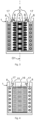
- Fig. 1 shows the cross-section view on a power module of a fully solid-state circuit breaker.
- the power module for the solid-state circuit breaker includes insulating material 12.
- the insulating material 12 is placed in a package 11 made of a thermally resistant plastic.
- the insulating material 12 is a silicone dielectric gel.
- the module includes a dielectric material heat sink 1 having thermal conductivity over 20 W/m/K. Aluminium nitride is suitable material for the heat sink 1. On its surface, the heat sink 1 is provided with an electrically conductive power pattern 3. An electrically conductive power pattern 3 comprises two electrically insulated sections.
- the electrically conductive power pattern 3 is applied directly on the heat sink 1 and no electric insulation needs to be used between the electrically conductive power pattern 3 and the heat sink 1 being made of electrically conductive material in known designs.
- a bi-directional power electronics switch 5 is placed on the electrically conductive power pattern 3 and connected by an electrically conductive power connection 2.
- the bi-directional power electronics switch 5 comprises power semiconductor bare dies being mutually interconnected with a power conductive connection 4.
- the power electronics switch 5 is located on longitudinal axis O1 of the module.
- the power circuit comprises anti-serial arrangement of semiconductor bare dies of the power electronics switch 5. These are two groups of six of SiC MOSFET transistor dies connected in parallel, and they are placed axially symmetrically as closest as possible to the centre of the power module on the heat sink 1 as shown in Fig. 3
- the electrically conductive power pattern 3 is interconnected with output power electric terminals 8. In addition, it is joined to the auxiliary dielectric substrates 9 via a contact layer 21.
- the contact layer 21 of the auxiliary dielectric substrate 9 comprises an electrically conductive layer 13 applied on the auxiliary dielectric substrate 9, and the electrically conductive power connection 2 of which full contact surfaces link the electrically conductive layer 13 and the electrically conductive power pattern 3 in a monolithic way.
- the non-power electric patterns 18 interconnect the non-power electronics circuits 7.
- the non-power electronics circuits 7 are interconnected with the output non-power electric terminals 17 and in addition, with the power electronics switch 5 via the non-power conductive connection 6.
- the heat sink 1, the power electronics switch 5, the auxiliary dielectric substrates 9, and the non-power electronics circuits 7 are jointly included in a monolithic multilayer structure elements of which are connected through entire contact surfaces.
- Optimum control of the power electronics switch 5 bare dies arranged in parallel is provided by a suitable electric connection with the non-power electronics circuits 7 .
- a suitable electric connection with the non-power electronics circuits 7 Thanks to thin layer of the electrically conductive non-power patterns 18 a necessary thin gap between the elements of the electrically conductive non-power pattern 18 is achieved allowing the use of the non-power electronics devices of SMD type with down to 0603 size.
- the non-power electronics circuit 7 is used for symmetric and electrically identical driving of the transistors connected in parallel, for attenuation of undesired oscillations that occur by the power electronics circuit operation, or for protection of the gate electrodes of the transistors.
- Use of the auxiliary dielectric substrate 9 causes that a multilayer interconnection structure is formed.
- the structure allows full use of heat sink 1 obverse side to carry high current load by the electrically conductive power patterns 3 and axially symmetrical placement of the semiconductor bare dies of the power electronics switch 5 (refer to Fig. 3 ).
- the structure allows placement and interconnection of the non-power electronics circuit 7 on the auxiliary dielectric substrate 9 to be at distance as shortest as possible from the power electronics switch 5.
- the auxiliary dielectric substrates 9 have the quality of electric insulation, thermal expansion properties and thermal conductivity properties identical to the heat sink 1 and therefore, the resulting properties of the power module are not influenced in any way.
- balancing (protective) resistors of Gate and Source electrodes are placed on the auxiliary dielectric substrates 9 separately for each power semiconductor bare die.
- auxiliary dielectric substrate 9 permits maximization of the surface of the electrically conductive power pattern 3 on the heat sink 1. This is favourable, in particular with respect to minimization of the current density, minimization of power losses, and thermal impedance of the power module. At the same time, higher volume of the electrically conductive pattern 3 allow accumulation of more thermal energy in case of transient phenomena.
- the output power electric terminals 8 and the output non-power electric terminals 17 are interconnected with the protective circuits 15 arranged on the substrate 16.
- the output terminals 8, 17 are provided as soldering pins.
- the electrically conductive power pattern 3, the electrically conductive non-power patterns 18 and electrically conductive layer 13 of the auxiliary dielectric substrate 9 are applied by an additive technology (printing technique). As illustrated in Fig. 1 , the electrically conductive power pattern 3 and the electrically conductive non-power patterns 18 have different thicknesses. The electrically conductive non-power pattern 18 is thinner than the electrically conductive power pattern 3 . Thicknesses of the layers range from 20 ⁇ m to 300 ⁇ m.
- the electrically conductive power connection 2 on the electrically conductive power pattern 3 and electrically conductive connection 10 of the auxiliary heat sink is a layer of solder.
- the power conductive connection 4 between the semiconductor bare dies of the bi-directional switch 5 and/or the non-power conductive connection 6 between the semiconductor bare dies of the bi-directional switch 5 and the non-power electronics circuit 7 are provided in the form of electrically conductive ribbons. More specifically, these are silver-plated copper ribbons.
- the power conductive connection 4 includes ribbons 4 mm wide and 200 ⁇ m thick. Compared to the wire-bonding technology, maximum transmitted current and reduction of the current density is permitted thereby not only in the power conductive connection 4 but also in the metallized area of the semiconductor bare die.
- the interconnection between the driving electrodes of the power electronics switch 5 bare dies and the non-power electronics circuit 7 is provided by 0.8 mm wide and 200 ⁇ m thick ribbons.
- FIG. 2 Another contemplated embodiment is shown in Fig. 2 and it differs from the one described above by that the dielectric material heat sink 1 is mechanically and thermally connected to the auxiliary heat sink 14 made of electrically conductive material having thermal conductivity over 180 W/m/K.
- a heat sink contact layer 20 is interconnecting the heat sink 1 and the auxiliary heat sink 14 while compensating their different thermal expansion properties.
- the contact layer 20 of the heat sink comprises an electrically conductive layer 19 applied on the heat sink 1 , and an electrically conductive connection 10 of which full contact surfaces interconnect the electrically conductive layer 19 and the auxiliary heat sink 14 in a monolithic way.
- the auxiliary heat sink 14 is made of aluminium
- the heat sink 1 is made of Al 2 O 3 .
- a power module of a solid-state circuit breaker finds its use in power applications in industry, services, or research and development, and where electricity is used with the need for safe operation.
Landscapes
- Engineering & Computer Science (AREA)
- Power Engineering (AREA)
- Physics & Mathematics (AREA)
- General Physics & Mathematics (AREA)
- Cooling Or The Like Of Semiconductors Or Solid State Devices (AREA)
Claims (9)
- Leistungsmodul für einen Halbleiter-Leistungsschutzschalter, das ein Isoliermaterial (12) umfasst, in dem ein bidirektionaler Leistungselektronik-Schalter (5) sowie nicht-leistungselektronische Schaltungen (7) mit Schutzelementen, Steuerkreisen für den Leistungselektronik-Schalter (5) und Sensorschaltungen angeordnet sind,ferner einen Kühlkörper (1) aus einem dielektrischen Material mit einer Wärmeleitfähigkeit von über 20 W/m/K, auf dessen Oberfläche ein elektrisch leitfähiges Leistungsmuster (3) aus Silber und/oder Kupfer angeordnet ist, wobei das elektrisch leitfähige Leistungsmuster (3) mindestens zwei elektrisch isolierte Abschnitte umfasst,wobei der bidirektionale Leistungselektronik-Schalter (5) Halbleiter-Chips in Form von Leistungshalbleitern umfasst, die durch eine leistungsleitende Verbindung (4) miteinander verbunden sind, und auf dem elektrisch leitfähigen Leistungsmuster (3) platziert sowie durch die elektrisch leitfähige Leistungsanschlussverbindung (2) verbunden ist, wobei der Leistungselektronik-Schalter (5) auf der Längsachse (O1) des Moduls positioniert ist, das elektrisch leitfähige Leistungsmuster (3) mit den elektrischen Ausgangsklemmen für die Leistung (8) verbunden ist und über eine Kontaktschicht (21) mit zusätzlichen dielektrischen Substraten (9) verbunden ist, auf denen elektrisch leitfähige nicht-leistungselektronische Muster (18) aus Silber und/oder Kupfer angeordnet sind, die die nicht-leistungselektronischen Schaltungen (7) auf den zusätzlichen dielektrischen Substraten (9) verbinden, wobei die genannte Kontaktschicht (21) der zusätzlichen dielektrischen Substrate (9) eine elektrisch leitfähige Schicht (13) umfasst, die auf die zusätzlichen dielektrischen Substrate (9) aufgebracht ist, und die elektrisch leitfähige Leistungsanschlussverbindung (2), deren vollständige Kontaktflächen die elektrisch leitfähige Schicht (13) und das elektrisch leitfähige Leistungsmuster (3) monolithisch verbinden,die nicht-leistungselektronischen Schaltungen (7) mit den nicht-leistungselektrischen Ausgangsklemmen (17) und mit dem Leistungselektronik-Schalter (5) über eine nicht-leistungsleitende Verbindung (6) verbunden sind,die elektrischen Ausgangsklemmen für die Leistung (8) und die nicht-leistungselektrischen Ausgangsklemmen (17) mit Schutzschaltungen (15) verbunden sind,wobei mindestens der Kühlkörper (1), der Leistungselektronik-Schalter (5), die zusätzlichen dielektrischen Substrate (9) und die nicht-leistungselektronischen Schaltungen (7) gemeinsam in eine monolithische mehrschichtige Struktur integriert sind, deren Teile durch vollständige Kontaktflächen verbunden sind.
- Leistungsmodul gemäß Anspruch 1, wobei der Kühlkörper (1) mechanisch und thermisch mit einem zusätzlichen Kühlkörper (14) aus elektrisch leitfähigem Material mit einer Wärmeleitfähigkeit von über 180 W/m/K durch eine Kontaktlage (20) verbunden ist, um unterschiedliche Wärmeausdehnungen des Kühlkörpers (1) und des zusätzlichen Kühlkörpers (14) auszugleichen.
- Leistungsmodul gemäß Anspruch 2, wobei die Kontaktlage (20) des Kühlkörpers eine elektrisch leitfähige Schicht (19) umfasst, die auf den Kühlkörper (1) aufgebracht ist, sowie eine elektrisch leitfähige Verbindung (10), deren vollständige Kontaktflächen die elektrisch leitfähige Schicht (19) und den zusätzlichen Kühlkörper (14) monolithisch verbinden.
- Leistungsmodul gemäß einem der vorhergehenden Ansprüche, wobei der Kühlkörper (1) und/oder die zusätzlichen dielektrischen Substrate (9) aus Keramik bestehen.
- Leistungsmodul gemäß einem der vorhergehenden Ansprüche, wobei der Leistungselektronik-Schalter (5) aus blanken Chips von rückleitenden Transistoren besteht, die in einer Antiserienschaltung angeordnet sind, oder aus blanken Chips mit rücksperrenden Transistoren, die in einer Antiparallelschaltung angeordnet sind.
- Leistungsmodul gemäß einem der vorhergehenden Ansprüche, wobei die elektrisch leitfähige Leistungsanschlussverbindung (2) auf dem elektrisch leitfähigen Leistungsmuster (3) und/oder die elektrisch leitfähige Verbindung (10) des zusätzlichen Kühlkörpers eine Lötverbindung oder eine gesinterte Materialschicht ist.
- Leistungsmodul gemäß einem der vorhergehenden Ansprüche, wobei die leistungsleitende Verbindung (4) zwischen den Halbleiter-Chips des bidirektionalen Leistungselektronik-Schalters (5) und/oder die nicht leistungsleitende Verbindung (6) zwischen den Halbleiter-Chips des bidirektionalen Leistungselektronik-Schalters (5) und der nicht leistungselektronischen Schaltung (7) in Form von Aluminium- und/oder Kupferdrähten und/oder elektrisch leitfähigen Bändern ausgeführt ist.
- Leistungsmodul gemäß einem der vorhergehenden Ansprüche, wobei das Isoliermaterial (12) in einem Gehäuse (11) untergebracht ist.
- Leistungsmodul gemäß einem der Ansprüche 1 bis 7, wobei das Isoliermaterial (12) selbsttragend ist und das Gehäuse (11) bildet.
Applications Claiming Priority (2)
| Application Number | Priority Date | Filing Date | Title |
|---|---|---|---|
| CZ2023-41A CZ310213B8 (cs) | 2023-01-31 | 2023-01-31 | Výkonový modul pro polovodičový jistič |
| PCT/CZ2024/050005 WO2024160308A1 (en) | 2023-01-31 | 2024-01-31 | Power module for solid-state circuit breaker |
Publications (3)
| Publication Number | Publication Date |
|---|---|
| EP4490780A1 EP4490780A1 (de) | 2025-01-15 |
| EP4490780B1 true EP4490780B1 (de) | 2025-05-14 |
| EP4490780C0 EP4490780C0 (de) | 2025-05-14 |
Family
ID=90417433
Family Applications (1)
| Application Number | Title | Priority Date | Filing Date |
|---|---|---|---|
| EP24713379.6A Active EP4490780B1 (de) | 2023-01-31 | 2024-01-31 | Leistungsmodul für festkörper-leistungsschutzschalter |
Country Status (3)
| Country | Link |
|---|---|
| EP (1) | EP4490780B1 (de) |
| CZ (1) | CZ310213B8 (de) |
| WO (1) | WO2024160308A1 (de) |
Citations (1)
| Publication number | Priority date | Publication date | Assignee | Title |
|---|---|---|---|---|
| WO2022056679A1 (zh) * | 2020-09-15 | 2022-03-24 | 华为技术有限公司 | 功率模组及其制造方法、转换器和电子设备 |
Family Cites Families (9)
| Publication number | Priority date | Publication date | Assignee | Title |
|---|---|---|---|---|
| US8018056B2 (en) * | 2005-12-21 | 2011-09-13 | International Rectifier Corporation | Package for high power density devices |
| JP2011254387A (ja) * | 2010-06-03 | 2011-12-15 | Rohm Co Ltd | 交流スイッチ |
| US9095054B1 (en) * | 2012-10-12 | 2015-07-28 | Arkansas Power Electronics International, Inc. | High temperature equalized electrical parasitic power packaging method for many paralleled semiconductor power devices |
| DE102014111931B4 (de) * | 2014-08-20 | 2021-07-08 | Infineon Technologies Ag | Niederinduktive Schaltungsanordnung mit Laststromsammelleiterbahn |
| US9839146B2 (en) * | 2015-10-20 | 2017-12-05 | Cree, Inc. | High voltage power module |
| US11373831B2 (en) * | 2019-05-18 | 2022-06-28 | Amber Solutions, Inc. | Intelligent circuit breakers |
| EP4088125A4 (de) * | 2020-01-21 | 2024-03-06 | Amber Semiconductor, Inc. | Intelligente schaltungsunterbrechung |
| WO2022005134A1 (ko) * | 2020-07-03 | 2022-01-06 | 주식회사 아모센스 | 파워모듈 |
| DE102021202197A1 (de) * | 2021-03-08 | 2022-09-08 | Robert Bosch Gesellschaft mit beschränkter Haftung | Leistungsmodul mit einem keramischen Schaltungsträger, einer flexiblen Leiterplatte und einem Temperatursensor |
-
2023
- 2023-01-31 CZ CZ2023-41A patent/CZ310213B8/cs unknown
-
2024
- 2024-01-31 WO PCT/CZ2024/050005 patent/WO2024160308A1/en not_active Ceased
- 2024-01-31 EP EP24713379.6A patent/EP4490780B1/de active Active
Patent Citations (2)
| Publication number | Priority date | Publication date | Assignee | Title |
|---|---|---|---|---|
| WO2022056679A1 (zh) * | 2020-09-15 | 2022-03-24 | 华为技术有限公司 | 功率模组及其制造方法、转换器和电子设备 |
| US20230215788A1 (en) * | 2020-09-15 | 2023-07-06 | Huawei Technologies Co., Ltd. | Power module and manufacturing method thereof, converter, and electronic device |
Also Published As
| Publication number | Publication date |
|---|---|
| WO2024160308A1 (en) | 2024-08-08 |
| EP4490780A1 (de) | 2025-01-15 |
| CZ310213B6 (cs) | 2024-11-27 |
| CZ202341A3 (cs) | 2024-08-07 |
| EP4490780C0 (de) | 2025-05-14 |
| CZ310213B8 (cs) | 2025-02-05 |
Similar Documents
| Publication | Publication Date | Title |
|---|---|---|
| CN110199388B (zh) | 用于并联功率装置的具有低电感和快速切换的高功率多层模块 | |
| US9116532B2 (en) | Power semiconductor device module | |
| US5463252A (en) | Modular solid state relay | |
| EP1160866B1 (de) | Halbleiterelement mit Leistungsverdrahtungsstruktur | |
| US5574312A (en) | Low-inductance power semiconductor module | |
| KR102792173B1 (ko) | 통합형 신호 보드를 구비한 상승된 전력 평면을 갖는 전력 모듈 및 이를 구현하는 방법 | |
| US11527456B2 (en) | Power module with organic layers | |
| CN111048491A (zh) | 电力用半导体模块以及电力变换装置 | |
| US20240258196A1 (en) | Inverter power module | |
| US11652091B2 (en) | Solid state switching device including nested control electronics | |
| US20210400815A1 (en) | Solid state switching device including heat sinks and control electronics construction | |
| WO2020229052A1 (en) | Power semiconductor module with low inductance gate crossing | |
| EP4490780B1 (de) | Leistungsmodul für festkörper-leistungsschutzschalter | |
| CN101809741B (zh) | 用于大电流的功率控制的具有至少一个半导体器件、尤其是功率半导体器件的装置 | |
| EP0431586B1 (de) | Hochleistungshalbleiterbauelement | |
| JP6305362B2 (ja) | 電力用半導体モジュール | |
| JP7156155B2 (ja) | 半導体モジュール | |
| JP2007096311A (ja) | 過電流防護装置を備えたパワー半導体モジュール | |
| CN108885940B (zh) | 模块 | |
| US20220199492A1 (en) | Semiconductor cooling arrangement with improved baffle | |
| CZ36911U1 (cs) | Výkonový modul pro polovodičový jistič | |
| US20240136343A1 (en) | Semiconductor module | |
| EP3660896A1 (de) | Halbleiteranordnung | |
| CN119314974B (zh) | 功率半导体封装结构 | |
| US20250174514A1 (en) | Power semiconductor switching module |
Legal Events
| Date | Code | Title | Description |
|---|---|---|---|
| STAA | Information on the status of an ep patent application or granted ep patent |
Free format text: STATUS: UNKNOWN |
|
| STAA | Information on the status of an ep patent application or granted ep patent |
Free format text: STATUS: THE INTERNATIONAL PUBLICATION HAS BEEN MADE |
|
| PUAI | Public reference made under article 153(3) epc to a published international application that has entered the european phase |
Free format text: ORIGINAL CODE: 0009012 |
|
| STAA | Information on the status of an ep patent application or granted ep patent |
Free format text: STATUS: REQUEST FOR EXAMINATION WAS MADE |
|
| 17P | Request for examination filed |
Effective date: 20241007 |
|
| AK | Designated contracting states |
Kind code of ref document: A1 Designated state(s): AL AT BE BG CH CY CZ DE DK EE ES FI FR GB GR HR HU IE IS IT LI LT LU LV MC ME MK MT NL NO PL PT RO RS SE SI SK SM TR |
|
| RIC1 | Information provided on ipc code assigned before grant |
Ipc: H01L 23/373 20060101ALN20241219BHEP Ipc: H01L 23/60 20060101ALN20241219BHEP Ipc: H01L 23/538 20060101ALN20241219BHEP Ipc: H01L 23/36 20060101ALN20241219BHEP Ipc: H01L 25/16 20230101ALI20241219BHEP Ipc: H01L 23/498 20060101ALI20241219BHEP Ipc: H01L 25/07 20060101ALI20241219BHEP Ipc: H01L 23/00 20060101ALI20241219BHEP Ipc: H01L 23/62 20060101AFI20241219BHEP |
|
| GRAP | Despatch of communication of intention to grant a patent |
Free format text: ORIGINAL CODE: EPIDOSNIGR1 |
|
| STAA | Information on the status of an ep patent application or granted ep patent |
Free format text: STATUS: GRANT OF PATENT IS INTENDED |
|
| RIC1 | Information provided on ipc code assigned before grant |
Ipc: H01L 23/373 20060101ALN20250114BHEP Ipc: H01L 23/60 20060101ALN20250114BHEP Ipc: H01L 23/538 20060101ALN20250114BHEP Ipc: H01L 23/36 20060101ALN20250114BHEP Ipc: H01L 25/16 20230101ALI20250114BHEP Ipc: H01L 23/498 20060101ALI20250114BHEP Ipc: H01L 25/07 20060101ALI20250114BHEP Ipc: H01L 23/00 20060101ALI20250114BHEP Ipc: H01L 23/62 20060101AFI20250114BHEP |
|
| INTG | Intention to grant announced |
Effective date: 20250124 |
|
| GRAS | Grant fee paid |
Free format text: ORIGINAL CODE: EPIDOSNIGR3 |
|
| GRAA | (expected) grant |
Free format text: ORIGINAL CODE: 0009210 |
|
| STAA | Information on the status of an ep patent application or granted ep patent |
Free format text: STATUS: THE PATENT HAS BEEN GRANTED |
|
| AK | Designated contracting states |
Kind code of ref document: B1 Designated state(s): AL AT BE BG CH CY CZ DE DK EE ES FI FR GB GR HR HU IE IS IT LI LT LU LV MC ME MK MT NL NO PL PT RO RS SE SI SK SM TR |
|
| DAV | Request for validation of the european patent (deleted) | ||
| DAX | Request for extension of the european patent (deleted) | ||
| REG | Reference to a national code |
Ref country code: GB Ref legal event code: FG4D |
|
| REG | Reference to a national code |
Ref country code: CH Ref legal event code: EP |
|
| REG | Reference to a national code |
Ref country code: DE Ref legal event code: R096 Ref document number: 602024000133 Country of ref document: DE |
|
| REG | Reference to a national code |
Ref country code: IE Ref legal event code: FG4D |
|
| U01 | Request for unitary effect filed |
Effective date: 20250612 |
|
| U07 | Unitary effect registered |
Designated state(s): AT BE BG DE DK EE FI FR IT LT LU LV MT NL PT RO SE SI Effective date: 20250624 |
|
| PG25 | Lapsed in a contracting state [announced via postgrant information from national office to epo] |
Ref country code: ES Free format text: LAPSE BECAUSE OF FAILURE TO SUBMIT A TRANSLATION OF THE DESCRIPTION OR TO PAY THE FEE WITHIN THE PRESCRIBED TIME-LIMIT Effective date: 20250514 |
|
| PG25 | Lapsed in a contracting state [announced via postgrant information from national office to epo] |
Ref country code: GR Free format text: LAPSE BECAUSE OF FAILURE TO SUBMIT A TRANSLATION OF THE DESCRIPTION OR TO PAY THE FEE WITHIN THE PRESCRIBED TIME-LIMIT Effective date: 20250815 Ref country code: NO Free format text: LAPSE BECAUSE OF FAILURE TO SUBMIT A TRANSLATION OF THE DESCRIPTION OR TO PAY THE FEE WITHIN THE PRESCRIBED TIME-LIMIT Effective date: 20250814 |
|
| PG25 | Lapsed in a contracting state [announced via postgrant information from national office to epo] |
Ref country code: PL Free format text: LAPSE BECAUSE OF FAILURE TO SUBMIT A TRANSLATION OF THE DESCRIPTION OR TO PAY THE FEE WITHIN THE PRESCRIBED TIME-LIMIT Effective date: 20250514 |
|
| PG25 | Lapsed in a contracting state [announced via postgrant information from national office to epo] |
Ref country code: HR Free format text: LAPSE BECAUSE OF FAILURE TO SUBMIT A TRANSLATION OF THE DESCRIPTION OR TO PAY THE FEE WITHIN THE PRESCRIBED TIME-LIMIT Effective date: 20250514 |
|
| PG25 | Lapsed in a contracting state [announced via postgrant information from national office to epo] |
Ref country code: RS Free format text: LAPSE BECAUSE OF FAILURE TO SUBMIT A TRANSLATION OF THE DESCRIPTION OR TO PAY THE FEE WITHIN THE PRESCRIBED TIME-LIMIT Effective date: 20250814 |
|
| PG25 | Lapsed in a contracting state [announced via postgrant information from national office to epo] |
Ref country code: IS Free format text: LAPSE BECAUSE OF FAILURE TO SUBMIT A TRANSLATION OF THE DESCRIPTION OR TO PAY THE FEE WITHIN THE PRESCRIBED TIME-LIMIT Effective date: 20250914 |
|
| PG25 | Lapsed in a contracting state [announced via postgrant information from national office to epo] |
Ref country code: SM Free format text: LAPSE BECAUSE OF FAILURE TO SUBMIT A TRANSLATION OF THE DESCRIPTION OR TO PAY THE FEE WITHIN THE PRESCRIBED TIME-LIMIT Effective date: 20250514 |
|
| PG25 | Lapsed in a contracting state [announced via postgrant information from national office to epo] |
Ref country code: CZ Free format text: LAPSE BECAUSE OF FAILURE TO SUBMIT A TRANSLATION OF THE DESCRIPTION OR TO PAY THE FEE WITHIN THE PRESCRIBED TIME-LIMIT Effective date: 20250514 |
|
| PG25 | Lapsed in a contracting state [announced via postgrant information from national office to epo] |
Ref country code: SK Free format text: LAPSE BECAUSE OF FAILURE TO SUBMIT A TRANSLATION OF THE DESCRIPTION OR TO PAY THE FEE WITHIN THE PRESCRIBED TIME-LIMIT Effective date: 20250514 |
|
| U20 | Renewal fee for the european patent with unitary effect paid |
Year of fee payment: 3 Effective date: 20260128 |
|
| PLBE | No opposition filed within time limit |
Free format text: ORIGINAL CODE: 0009261 |
|
| STAA | Information on the status of an ep patent application or granted ep patent |
Free format text: STATUS: NO OPPOSITION FILED WITHIN TIME LIMIT |
|
| REG | Reference to a national code |
Ref country code: CH Ref legal event code: L10 Free format text: ST27 STATUS EVENT CODE: U-0-0-L10-L00 (AS PROVIDED BY THE NATIONAL OFFICE) Effective date: 20260325 |
|
| PGFP | Annual fee paid to national office [announced via postgrant information from national office to epo] |
Ref country code: MC Payment date: 20260128 Year of fee payment: 3 |
|
| PGFP | Annual fee paid to national office [announced via postgrant information from national office to epo] |
Ref country code: IE Payment date: 20260128 Year of fee payment: 3 |
|
| 26N | No opposition filed |
Effective date: 20260217 |