EP4489554A1 - Organisches lichtemittierendes element, verfahren zur beurteilung von verzögertem fluoreszenzmaterial, verfahren zum entwurf von verzögertem fluoreszenzmaterial - Google Patents
Organisches lichtemittierendes element, verfahren zur beurteilung von verzögertem fluoreszenzmaterial, verfahren zum entwurf von verzögertem fluoreszenzmaterial Download PDFInfo
- Publication number
- EP4489554A1 EP4489554A1 EP23763530.5A EP23763530A EP4489554A1 EP 4489554 A1 EP4489554 A1 EP 4489554A1 EP 23763530 A EP23763530 A EP 23763530A EP 4489554 A1 EP4489554 A1 EP 4489554A1
- Authority
- EP
- European Patent Office
- Prior art keywords
- delayed fluorescent
- fluorescent material
- formula
- light emitting
- group
- Prior art date
- Legal status (The legal status is an assumption and is not a legal conclusion. Google has not performed a legal analysis and makes no representation as to the accuracy of the status listed.)
- Pending
Links
Images


Classifications
-
- H—ELECTRICITY
- H10—SEMICONDUCTOR DEVICES; ELECTRIC SOLID-STATE DEVICES NOT OTHERWISE PROVIDED FOR
- H10K—ORGANIC ELECTRIC SOLID-STATE DEVICES
- H10K85/00—Organic materials used in the body or electrodes of devices covered by this subclass
- H10K85/60—Organic compounds having low molecular weight
- H10K85/649—Aromatic compounds comprising a hetero atom
- H10K85/657—Polycyclic condensed heteroaromatic hydrocarbons
- H10K85/6572—Polycyclic condensed heteroaromatic hydrocarbons comprising only nitrogen in the heteroaromatic polycondensed ring system, e.g. phenanthroline or carbazole
-
- C—CHEMISTRY; METALLURGY
- C09—DYES; PAINTS; POLISHES; NATURAL RESINS; ADHESIVES; COMPOSITIONS NOT OTHERWISE PROVIDED FOR; APPLICATIONS OF MATERIALS NOT OTHERWISE PROVIDED FOR
- C09K—MATERIALS FOR MISCELLANEOUS APPLICATIONS, NOT PROVIDED FOR ELSEWHERE
- C09K11/00—Luminescent materials, e.g. electroluminescent or chemiluminescent
- C09K11/06—Luminescent materials, e.g. electroluminescent or chemiluminescent containing organic luminescent materials
-
- G—PHYSICS
- G01—MEASURING; TESTING
- G01N—INVESTIGATING OR ANALYSING MATERIALS BY DETERMINING THEIR CHEMICAL OR PHYSICAL PROPERTIES
- G01N21/00—Investigating or analysing materials by the use of optical means, i.e. using sub-millimetre waves, infrared, visible or ultraviolet light
- G01N21/62—Systems in which the material investigated is excited whereby it emits light or causes a change in wavelength of the incident light
- G01N21/63—Systems in which the material investigated is excited whereby it emits light or causes a change in wavelength of the incident light optically excited
- G01N21/64—Fluorescence; Phosphorescence
- G01N21/6408—Fluorescence; Phosphorescence with measurement of decay time, time resolved fluorescence
-
- G—PHYSICS
- G06—COMPUTING OR CALCULATING; COUNTING
- G06F—ELECTRIC DIGITAL DATA PROCESSING
- G06F30/00—Computer-aided design [CAD]
- G06F30/20—Design optimisation, verification or simulation
-
- H—ELECTRICITY
- H10—SEMICONDUCTOR DEVICES; ELECTRIC SOLID-STATE DEVICES NOT OTHERWISE PROVIDED FOR
- H10K—ORGANIC ELECTRIC SOLID-STATE DEVICES
- H10K71/00—Manufacture or treatment specially adapted for the organic devices covered by this subclass
- H10K71/70—Testing, e.g. accelerated lifetime tests
-
- H—ELECTRICITY
- H10—SEMICONDUCTOR DEVICES; ELECTRIC SOLID-STATE DEVICES NOT OTHERWISE PROVIDED FOR
- H10K—ORGANIC ELECTRIC SOLID-STATE DEVICES
- H10K85/00—Organic materials used in the body or electrodes of devices covered by this subclass
- H10K85/60—Organic compounds having low molecular weight
- H10K85/615—Polycyclic condensed aromatic hydrocarbons, e.g. anthracene
-
- H—ELECTRICITY
- H10—SEMICONDUCTOR DEVICES; ELECTRIC SOLID-STATE DEVICES NOT OTHERWISE PROVIDED FOR
- H10K—ORGANIC ELECTRIC SOLID-STATE DEVICES
- H10K85/00—Organic materials used in the body or electrodes of devices covered by this subclass
- H10K85/60—Organic compounds having low molecular weight
- H10K85/649—Aromatic compounds comprising a hetero atom
- H10K85/654—Aromatic compounds comprising a hetero atom comprising only nitrogen as heteroatom
-
- H—ELECTRICITY
- H10—SEMICONDUCTOR DEVICES; ELECTRIC SOLID-STATE DEVICES NOT OTHERWISE PROVIDED FOR
- H10K—ORGANIC ELECTRIC SOLID-STATE DEVICES
- H10K85/00—Organic materials used in the body or electrodes of devices covered by this subclass
- H10K85/60—Organic compounds having low molecular weight
- H10K85/649—Aromatic compounds comprising a hetero atom
- H10K85/657—Polycyclic condensed heteroaromatic hydrocarbons
-
- C—CHEMISTRY; METALLURGY
- C09—DYES; PAINTS; POLISHES; NATURAL RESINS; ADHESIVES; COMPOSITIONS NOT OTHERWISE PROVIDED FOR; APPLICATIONS OF MATERIALS NOT OTHERWISE PROVIDED FOR
- C09K—MATERIALS FOR MISCELLANEOUS APPLICATIONS, NOT PROVIDED FOR ELSEWHERE
- C09K2211/00—Chemical nature of organic luminescent or tenebrescent compounds
- C09K2211/10—Non-macromolecular compounds
- C09K2211/1003—Carbocyclic compounds
- C09K2211/1007—Non-condensed systems
-
- C—CHEMISTRY; METALLURGY
- C09—DYES; PAINTS; POLISHES; NATURAL RESINS; ADHESIVES; COMPOSITIONS NOT OTHERWISE PROVIDED FOR; APPLICATIONS OF MATERIALS NOT OTHERWISE PROVIDED FOR
- C09K—MATERIALS FOR MISCELLANEOUS APPLICATIONS, NOT PROVIDED FOR ELSEWHERE
- C09K2211/00—Chemical nature of organic luminescent or tenebrescent compounds
- C09K2211/10—Non-macromolecular compounds
- C09K2211/1003—Carbocyclic compounds
- C09K2211/1011—Condensed systems
-
- C—CHEMISTRY; METALLURGY
- C09—DYES; PAINTS; POLISHES; NATURAL RESINS; ADHESIVES; COMPOSITIONS NOT OTHERWISE PROVIDED FOR; APPLICATIONS OF MATERIALS NOT OTHERWISE PROVIDED FOR
- C09K—MATERIALS FOR MISCELLANEOUS APPLICATIONS, NOT PROVIDED FOR ELSEWHERE
- C09K2211/00—Chemical nature of organic luminescent or tenebrescent compounds
- C09K2211/10—Non-macromolecular compounds
- C09K2211/1018—Heterocyclic compounds
-
- H—ELECTRICITY
- H10—SEMICONDUCTOR DEVICES; ELECTRIC SOLID-STATE DEVICES NOT OTHERWISE PROVIDED FOR
- H10K—ORGANIC ELECTRIC SOLID-STATE DEVICES
- H10K2101/00—Properties of the organic materials covered by group H10K85/00
- H10K2101/10—Triplet emission
-
- H—ELECTRICITY
- H10—SEMICONDUCTOR DEVICES; ELECTRIC SOLID-STATE DEVICES NOT OTHERWISE PROVIDED FOR
- H10K—ORGANIC ELECTRIC SOLID-STATE DEVICES
- H10K2101/00—Properties of the organic materials covered by group H10K85/00
- H10K2101/20—Delayed fluorescence emission
-
- H—ELECTRICITY
- H10—SEMICONDUCTOR DEVICES; ELECTRIC SOLID-STATE DEVICES NOT OTHERWISE PROVIDED FOR
- H10K—ORGANIC ELECTRIC SOLID-STATE DEVICES
- H10K2101/00—Properties of the organic materials covered by group H10K85/00
- H10K2101/27—Combination of fluorescent and phosphorescent emission
-
- H—ELECTRICITY
- H10—SEMICONDUCTOR DEVICES; ELECTRIC SOLID-STATE DEVICES NOT OTHERWISE PROVIDED FOR
- H10K—ORGANIC ELECTRIC SOLID-STATE DEVICES
- H10K2101/00—Properties of the organic materials covered by group H10K85/00
- H10K2101/30—Highest occupied molecular orbital [HOMO], lowest unoccupied molecular orbital [LUMO] or Fermi energy values
-
- H—ELECTRICITY
- H10—SEMICONDUCTOR DEVICES; ELECTRIC SOLID-STATE DEVICES NOT OTHERWISE PROVIDED FOR
- H10K—ORGANIC ELECTRIC SOLID-STATE DEVICES
- H10K50/00—Organic light-emitting devices
- H10K50/10—OLEDs or polymer light-emitting diodes [PLED]
- H10K50/11—OLEDs or polymer light-emitting diodes [PLED] characterised by the electroluminescent [EL] layers
- H10K50/12—OLEDs or polymer light-emitting diodes [PLED] characterised by the electroluminescent [EL] layers comprising dopants
Definitions
- the present invention relates to an organic light emitting device having high durability, a method for designing the organic light emitting device, a method for evaluating a delayed fluorescent material that is useful as a material for the organic light emitting device, a method for designing the delayed fluorescent material, and a program for carrying out these methods.
- organic light emitting devices such as organic electroluminescent devices (organic EL devices) are being conducted actively.
- various kinds of efforts have been made to increase the light emission efficiency of organic light-emitting devices by newly developing the materials constituting the devices.
- a delayed fluorescent material is a compound which, in an excited state, undergoes reverse intersystem crossing from an excited triplet state to an excited singlet state and then emits fluorescence when returning back from the excited singlet state to a ground state thereof. Fluorescence emitted through such a route is observed later than fluorescence from the excited singlet state directly occurring from the ground state (ordinary fluorescence), and is therefore referred to as delayed fluorescence.
- delayed fluorescence for example, in a case where an organic molecule is excited through carrier injection, the probability of occurrence of the excited singlet state to that of the excited triplet state is statistically 25% : 75%. Therefore, in conventional fluorescent materials that utilize only the energy of the excited singlet state occurring directly from the ground state, there is a limitation in the improvement of light emission efficiency.
- PBHT value index values that indicate the degree of overlap of the HOMO orbital and the LUMO orbital
- NPL 1 J. Chem. Phys. 128, 044118 (2008 )
- the present inventors conducted intensive investigations for the purpose of providing an organic light emitting device that contains a delayed fluorescent material in a light emitting layer and has excellent light emission efficiency.
- an organic light emitting device having high light emission efficiency can be provided when a delayed fluorescent material whose PBHT value in consideration of a higher triplet state and whose transition dipole moment satisfy specific conditions is used.
- the invention has been proposed based on these findings and specifically has the following configurations.
- an organic light emitting device having excellent light emission characteristics can be realized by using a delayed fluorescent material having a transition dipole moment of greater than 1 and a ⁇ PBHT(Tn-T2) of 0.02 or more. Furthermore, according to the method for evaluating a delayed fluorescent material of the invention, the light emission characteristics of a delayed fluorescent material, such as the light emission efficiency, can be easily evaluated. In addition, according to the method for designing a delayed fluorescent material of the invention, a delayed fluorescent material having satisfactory light emission characteristics can be designed.
- a numerical value range expressed herein using the term “to” means a range that includes the numerical values described before and after the term “to” as the lower limit value and the upper limit value.
- the term “consisting of” as used herein means consisting of only those items described after the term “consisting of", and does not include anything else.
- a hydrogen atom is expressed as H, or expression thereof is omitted.
- H is bonded to the ring skeleton-constituting carbon atom at the site where the expression is omitted.
- substituted as used in the present specification means an atom or an atomic group other than a hydrogen atom and a deuterium atom.
- the expressions "substituted or unsubstituted” and “may be substituted” mean that a hydrogen atom may be substituted with a deuterium atom or a substituted.
- the term "transparent” as used herein means that the transmittance to visible light is 50% or higher, preferably 80% or higher, more preferably 90% or higher, and even more preferably 99% or higher.
- the transmittance to visible light can be measured using an ultraviolet and visible spectrophotometer.
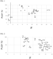
- An organic light emitting device of the invention has a light emitting layer containing a delayed fluorescent material that satisfies the following formula (I) and the following formula (II): ⁇ > 1 ⁇ PBHT Tn ⁇ T 2 > 0.02
- ⁇ represents the transition dipole moment of a delayed fluorescent material.
- a transition dipole moment indicates the degree of charge imbalance due to transition. As the value is larger, the degree of charge imbalance is greater, and the speed at which excitons return from an excited state to the ground state tends to be faster.
- the transition dipole moment is determined by molecular orbital calculation using quantum chemical calculation B3LYP/6-31G.
- ⁇ is greater than 1, preferably greater than 2, more preferably greater than 3, and even more preferably greater than 4. Furthermore, ⁇ is preferably less than 20, more preferably less than 17, and for example, ⁇ may be selected from the range of 13 or less or may be selected from the range of less than 8. In an aspect of the invention, ⁇ is selected from the range of greater than 4 and less than 8. In an aspect of the invention, ⁇ is selected from the range of greater than 9 and less than 13.
- ⁇ PBHT(Tn-T2) is represented by the following formula.
- ⁇ PBHT Tn ⁇ T 2 PBHT Tn ⁇ PBHT T2
- PBHT(T2) is a PBHT value of a second excited triplet state of a delayed fluorescent material
- PBHT(Tn) is a PBHT value of an n-th excited triplet state of a delayed fluorescent material.
- n represents 3 or 4.
- E T2 - E S1 ⁇ 0.1 eV, E T3 - E T2 ⁇ 0.1 eV, or both of these formulae are satisfied, n is 4, while otherwise, n is 3.
- E T2 represents the energy of a second excited triplet state T2
- E S1 represents the energy of the lowest excited singlet state S1
- E T3 represents the energy of a third excited triplet state T3.
- the energy of the lowest excited singlet state S1 and the energy of the lowest excited triplet state T1 can be determined by the following procedure. Furthermore, the energy of higher excited triplet states Tn such as a second excited triplet state T2, a third excited triplet state T3, and a fourth excited triplet state T4 can be determined by molecular orbital calculation using quantum chemical calculation B3LYP/6-31G.
- the "PBHT value” is a value proposed by Michael J. Peach, Peter Benfield, Trygve Helgaker, and David J. Tozer, and is a value named after the initials of the four surnames.
- the PBHT value is a numerical value that represents the orbital properties of an excited state.
- a small PBHT value indicates that the excited state is charge-transfer (CT)-related, and a large PBHT value indicates that the excited state is localized electron (LE)-related.
- the PBHT value indicates the degree of overlap between the highest occupied molecular orbital (HOMO) and the lowest unoccupied molecular orbital (LUMO) and takes a value of 0 or greater and 1 or less.
- a PBHT value of 0 indicates that there is no overlap between the HOMO and the LUMO, and a PBHT value of 1 indicates that the HOMO and the LUMO overlap completely.
- a delayed fluorescent material having a ⁇ PBHT(Tn-T2) of greater than 0.02 is used.
- the ⁇ PBHT(Tn-T2) of the delayed fluorescent material is preferably less than 0.40, more preferably less than 0.30, even more preferably less than 0.20, and still more preferably less than 0.11.
- a delayed fluorescent material having a ⁇ PBHT(Tn-T2) of greater than 0.02 and less than 0.10 is used.
- a delayed fluorescent material having a ⁇ PBHT(Tn-T2) of greater than 0.02 and less than 0.09 is used.
- a delayed fluorescent material having a ⁇ PBHT(Tn-T2) of greater than 0.02 and less than 0.05 can be used.
- a delayed fluorescent material having a ⁇ PBHT(Tn-T2) of greater than 0.05 and less than 0.09 can be used.
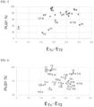
- the delayed fluorescent material used in the invention satisfies formula (I) and formula (II) and also further satisfies the following formula (III): E Tn ⁇ E T2 > 0.2 eV in formula (III), E Tn represents the energy of an n-th excited triplet state Tn, and E T2 represents the energy of a second excited triplet state T2.
- n as used herein has the same value as the n employed in formula (II) and is either 3 or 4. It is more preferable that the delayed fluorescent material used in the invention has an E Tn - E T2 value of greater than 0.2 eV and less than 0.5 eV
- the delayed fluorescent material used in the invention satisfies formula (I) and formula (II) and also further satisfies the following conditions.
- ⁇ PBHT(T2-T1) may be selected from the range of greater than 0 and less than 0.04, or may be selected from the range of greater than 0.04 and less than 0.08.
- ⁇ PBHT(T3-T1) may be selected from the range of greater than 0 and less than 0.04, or may be selected from the range of greater than 0.04 and less than 0.08.
- a delayed fluorescent material satisfying formula (I) and formula (II), which can be used in the invention, will be described in detail below.
- the “delayed fluorescent material” is an organic compound that undergoes reverse intersystem crossing from an excited triplet state to an excited singlet state in an excited state, and emanates fluorescence (delayed fluorescence) when returning from the excited singlet state to the ground state.
- a material in which when the emission lifetime is measured using a fluorescence lifetime measurement system such as a streak camera system manufactured by HAMAMATSU PHOTONICS K.K.
- fluorescence with an emission lifetime of 100 ns (nanoseconds) or more is observed is referred to as a delayed fluorescent material.
- a delayed fluorescent material having a ⁇ of greater than 1 and less than 20 and a ⁇ PBHT(Tn-T2) of greater than 0.02 and less than 0.40 is used.
- a delayed fluorescent material having a ⁇ of greater than 1 and less than 17 and a ⁇ PBHT(Tn-T2) of greater than 0.02 and less than 0.20 is used.
- a delayed fluorescent material having a ⁇ of greater than 4 and less than 17 and a ⁇ PBHT(Tn-T2) of greater than 0.02 and less than 0.11 is used.
- a delayed fluorescent material having a ⁇ of greater than 4 and less than 8 and a ⁇ PBHT(Tn-T2) of greater than 0.02 and less than 0.09 is used.
- the difference ⁇ E ST between the lowest excited singlet energy and the lowest excited triplet energy at 77 K is 0.3 eV or less, more preferably 0.25 eV or less, more preferably 0.2 eV or less, more preferably 0.15 eV or less, even more preferably 0.1 eV or less, still more preferably 0.07 eV or less, even more preferably 0.05 eV or less, still more preferably 0.03 eV or less, and particularly preferably 0.01 eV or less.
- the delayed fluorescent material satisfying formula (I) and formula (II) does not contain a metal atom.
- a compound consisting of atoms selected from the group consisting of a carbon atom, a hydrogen atom, a nitrogen atom, an oxygen atom, and a sulfur atom can be selected.
- a compound consisting of atoms selected from the group consisting of a carbon atom, a hydrogen atom, a nitrogen atom, and an oxygen atom can be selected.
- a compound consisting of a carbon atom, a hydrogen atom, and a nitrogen atom can be selected.
- the delayed fluorescent material satisfying formula (I) and formula (II) can be selected from, for example, a group of compounds having a structure in which an aromatic hydrocarbon is substituted with one or more electron-withdrawing groups and one or more electron-donating groups.
- the aromatic ring constituting the aromatic hydrocarbon may be a monocyclic ring or a fused ring in which two or more rings are fused.
- a preferred example of the aromatic ring may be a benzene ring.
- the electron-withdrawing group is a group having a property of withdrawing electrons from the ring to which the electron-withdrawing group is bonded, and can be selected from, for example, groups having a positive Hammett ⁇ p value.
- the electron-donating group is a group having a property of donating electrons to the ring to which the electron-donating group is bonded, and can be selected from, for example, groups having a negative Hammett ⁇ p value.
- the "Hammett ⁇ p value” is a value proposed by L.P. Hammett to quantify the effect of substituents on the reaction rate or equilibrium of para-substituted benzene derivatives.
- the "Hammett ⁇ p value” and the numerical value of each substituent in the present invention reference can be made to the description on the ⁇ p value in Hansch, C. et. al., Chem. Rev., 91, 165-195 (1991 ).
- Examples of an acceptor group include a cyano group and a six-membered aromatic heterocyclic group containing a nitrogen atom as a ring skeleton-constituting atom.
- Examples of the 6-membered aromatic heterocyclic group containing a nitrogen atom as a ring skeleton-constituting atom include a substituted or unsubstituted pyridyl group, a substituted or unsubstituted pyrimidyl group, a substituted or unsubstituted pyridazyl group, a substituted or unsubstituted pyrazyl group, and a substituted or unsubstituted triazyl group.
- Examples of a donor group include a substituted or unsubstituted diphenylamino group and a group represented by general formula (7) that will be described below.
- D 1 to D 10 each independently represent a group represented by the following general formula (7).
- each of the combinations of D 1 and D 2 , D 3 and D 4 , D 6 and D 7 , and D 9 and D 10 have chemical structures that are different from each other, and each combination of two D 1 , three D 2 , two D 3 , two D 4 , three D 5 , two D 6 , two D 8 , and two D 9 have chemical structures that are identical with each other.
- At least one hydrogen atom in the general formulae (1) to (6) and the following general formulae (7) to (13) may be substituted with a deuterium atom.
- the group represented by general formula (7) is a group represented by any of the following general formulae (8) to (13).
- L 11 and L 21 to L 26 each represent a single bond or a divalent linking group.
- the divalent linking group include a substituted or unsubstituted arylene group and a substituted or unsubstituted heteroarylene group.
- R 41 to R 110 each independently represent a hydrogen atom or a substituent.
- the cyclic structure formed by bonding to each other may be an aromatic ring or an aliphatic ring and may contain a heteroatom, and the cyclic structure may be a fused ring of two or more rings.
- the heteroatom as used herein is preferably selected from the group consisting of a nitrogen atom, an oxygen atom, and a sulfur atom.
- Examples of the cyclic structure to be formed include a benzene ring, a naphthalene ring, a pyridine ring, a pyridazine ring, a pyrimidine ring, a pyrazine ring, a pyrrole ring, an imidazole ring, a pyrazole ring, an imidazoline ring, an oxazole ring, an isoxazole ring, a thiazole ring, an isothiazole, ring, a cyclohexadiene ring, a cyclohexene ring, a cyclopentene ring, a cycloheptatriene ring, a cycloheptadiene ring, a cycloheptene ring, a furan ring, a thiophene ring, a naphthyridine ring, a quinoxaline ring, and a
- a ring in which a number of rings are fused such as a phenanthrene ring or a triphenylene ring, may be formed.
- the number of rings included in the group represented by general formula (7) may be selected from the range of 3 to 5, or may be selected from the range of 5 to 7.
- the number of rings included in the group represented by any of general formulae (8) to (13) may be selected from the range of 5 to 7, or may be 5.
- R 41 to R 110 examples include groups in the following substituent group B, and the substituent is preferably an unsubstituted alkyl group having 1 to 10 carbon atoms, or an aryl group having 6 to 10 carbon atoms which may be substituted with an unsubstituted alkyl group having 1 to 10 carbon atoms.
- R 41 to R 110 are each a hydrogen atom or an unsubstituted alkyl group having 1 to 10 carbon atoms.
- R 41 to R 110 are each a hydrogen atom or an unsubstituted aryl group having 6 to 10 carbon atoms.
- all of R 41 to R 110 are hydrogen atoms.
- the carbon atoms to which R 41 to R 110 are bonded (ring skeleton-constituting carbon atoms) in general formulae (7) to (13) may be each independently substituted with a nitrogen atom. That is, C-R 41 to C-R 110 in general formulae (7) to (13) may be each independently substituted with N.
- the number of substitutions with a nitrogen atom is preferably 0 to 4, and more preferably 1 or 2, in the group represented by any of general formulae (7) to (13). According to an aspect of the invention, the number of substitutions with a nitrogen atom is 0. Furthermore, when there are two or more substitutions with a nitrogen atom, the number of substitutions with a nitrogen atom in one ring is preferably 1.
- X 1 to X 6 each represent an oxygen atom, a sulfur atom, or N-R. According to an aspect of the invention, X 1 to X 6 are each an oxygen atom. According to an aspect of the invention, X 1 to X 6 are each a sulfur atom. According to an aspect of the invention, X 1 to X 6 are each N-R. R represents a hydrogen atom or a substituent, and is preferably a substituent. Examples of the substituent include substituents selected from the above-described substituent group A.
- an unsubstituted phenyl group, or a phenyl group substituted with one group, or a group obtained by combining two or more groups, selected from the group consisting of an alkyl group and an aryl group can be preferably employed.
- the symbol * represents a bonding position.
- the group represented by general formula (7) may be a substituted or unsubstituted 9-carbazolyl group, or may be an aryl group substituted with a substituted or unsubstituted 9-carbazolyl group, or a heteroaryl group substituted with a substituted or unsubstituted 9-carbazolyl group.
- a preferred position of the substituent in the 9-carbazolyl group is at least one of the 3-position and the 6-position.
- At least one of the groups represented by general formula (7) is preferably a group represented by any of general formulae (8) to (13). That is, it is preferable that at least one of D 1 and D 2 in general formula (1), at least one of D 3 and D 4 in general formula (2), D 5 in general formula (3), at least one of D 6 and D 7 in general formula (4), D 8 in general formula (5), and at least one of D 9 and D 10 in general formula (6) is a group represented by any of general formulae (8) to (13).
- D 2 , D 4 , D 6 , and D 9 are each a group represented by any of general formulae (8) to (13), and D 1 , D 3 , D 7 , and D 10 are each a substituted or unsubstituted 9-carbazolyl group, an aryl group substituted with a substituted or unsubstituted 9-carbazolyl group, or a heteroaryl group substituted with a substituted or unsubstituted 9-carbazolyl group.
- Ar 1 and Ar 2 each independently represent a substituted or unsubstituted aryl group or a substituted or unsubstituted heteroaryl group (provided that a group represented by general formula (7) is excluded).
- Ar 1 and Ar 2 are each preferably a substituted or unsubstituted aryl group, more preferably a substituted or unsubstituted phenyl group, and even more preferably an unsubstituted phenyl group or a phenyl group having at least one hydrogen atom substituted with a deuterium atom.
- the delayed fluorescent material is a compound represented by general formula (2), in which the PBHT(Tn) is PBHT(T3) of the third excited triplet state.
- the delayed fluorescent material is a compound represented by general formula (2), in which D 4 is a group represented by general formula (13), and the PBHT(Tn) is PBHT(T3) of the third excited triplet state.
- the delayed fluorescent material is a compound represented by general formula (4) or (5).
- the delayed fluorescent material is a compound represented by general formula (4), in which D 6 is a group represented by general formula (13).
- the delayed fluorescent material is a compound represented by general formula (5), in which D 8 is a group represented by general formula (13).
- the delayed fluorescent material has a symmetric structure.
- the delayed fluorescent material has an axisymmetric structure.
- delayed fluorescent material satisfying formula (I) and formula (II), which can be used in the present invention will be described below.
- the delayed fluorescent material that can be used in the invention should not be construed as being limited to these specific examples.
- alkyl group can be any of linear, branched or cyclic ones. Two or more of a linear moiety, a cyclic moiety and a branched moiety can be in the group as mixed.
- the carbon number of the alkyl group can be, for example, 1 or more, 2 or more, or 4 or more. The carbon number can also be 30 or less, 20 or less, 10 or less, 6 or less, or 4 or less.
- alkyl group examples include a methyl group, an ethyl group, an n-propyl group, an isopropyl group, an n-butyl group, an isobutyl group, a tert-butyl group, an n-pentyl group, an isopentyl group, an n-hexyl group, an isohexyl group, a 2-ethylhexyl group, an n-heptyl group, an isoheptyl group, an n-octyl group, an isooctyl group, an n-nonyl group, an isononyl group, an n-decanyl group, an isodecanyl group, a cyclopentyl group, a cyclohexyl group, and a cycloheptyl group.
- the alkyl group as a substituent may be further substituted with an aryl group.
- alkenyl group can be linear, branched or cyclic. Two or more of a linear moiety, a cyclic moiety and a branched moiety can be in the group as mixed.
- the carbon number of the alkenyl group can be, for example, 2 or more, or 4 or more. The carbon number can also be 30 or less, 20 or less, 10 or less, 6 or less, or 4 or less.
- alkenyl group examples include an ethenyl group, an n-propenyl group, an isopropenyl group, an n-butenyl group, an isobutenyl group, an n-pentenyl group, an isopentenyl group, an n-hexenyl group, an isohexenyl group, and a 2-ethylhexenyl group.
- the alkenyl group which is the substituent can be further substituted with a substituent.
- the "aryl group” and the “heteroaryl group” may be each a monocyclic ring or may be each a fused ring in which two or more rings are fused.
- the number of rings that are fused is preferably 2 to 6, and for example, the number of rings can be selected from 2 to 4.
- the ring include a benzene ring, a pyridine ring, a pyrimidine ring, a triazine ring, a naphthalene ring, an anthracene ring, a phenanthrene ring, a triphenylene ring, a quinoline ring, a pyrazine ring, a quinoxaline ring, and a naphthyridine ring, and the ring may be a fused ring of these.
- aryl group or a heteroaryl group examples include a phenyl group, a 1-naphthyl group, a 2-naphthyl group, a 1-anthracenyl group, a 2-anthracenyl group, a 9-anthracenyl group, a 2-pyridyl group, a 3-pyridyl group, and a 4-pyridyl group.
- the number of ring skeleton-constituting atoms of the aryl group is preferably 6 to 40, and more preferably 6 to 20, and may be selected from the range of 6 to 14 or may be selected from the range of 6 to 10.
- the number of ring skeleton-constituting atoms of the heteroaryl group is preferably 4 to 40, and more preferably 5 to 20, and may be selected from the range of 5 to 14 or may be selected from the range of 5 to 10.
- arylene group and heteroarylene group can be understood to mean groups in which the valence in the description of the aryl group and the heteroaryl group is changed from 1 to 2.
- the "substituent group A" in the present specification means one group, or a group obtained by combining two or more groups, selected from the group consisting of a hydroxyl group, a halogen atom (for example, a fluorine atom, a chlorine atom, a bromine atom, or an iodine atom), an alkyl group (for example, having 1 to 40 carbon atoms), an alkoxy group (for example, having 1 to 40 carbon atoms), an alkylthio group (for example, having 1 to 40 carbon atoms), an aryl group (for example, having 6 to 30 carbon atoms), an aryloxy group (for example, having 6 to 30 carbon atoms), an arylthio group (for example, having 6 to 30 carbon atoms), a heteroaryl group (for example, the number of ring skeleton-constituting atoms is 5 to 30), a heteroaryloxy group (for example, the number of ring skeleton-const
- the "substituent group B" in the present specification means one group, or a group obtained by combining two or more groups, selected from the group consisting of an alkyl group (for example, having 1 to 40 carbon atoms), an alkoxy group (for example, having 1 to 40 carbon atoms), an aryl group (for example having 6 to 30 carbon atoms), an aryloxy group (for example, having 6 to 30 carbon atoms), a heteroaryl group (for example, the number of ring skeleton-constituting atoms is 5 to 30), a heteroaryloxy group (for example, the number of ring skeleton-constituting atoms is 5 to 30), and a diarylaminoamino group (for example, the number of carbon atoms is 0 to 20).
- an alkyl group for example, having 1 to 40 carbon atoms
- an alkoxy group for example, having 1 to 40 carbon atoms
- an aryl group for example having 6 to 30 carbon
- substituted group C in the present specification means one group, or a group obtained by combining two or more groups, selected from the group consisting of an alkyl group (for example, having 1 to 20 carbon atoms), an aryl group (for example, having 6 to 22 carbon atoms), a heteroaryl group (for example, the number of ring skeleton-constituting atoms is 5 to 20), and a diarylamino group (for example, the number of carbon atoms is 12 to 20).
- an alkyl group for example, having 1 to 20 carbon atoms
- an aryl group for example, having 6 to 22 carbon atoms
- a heteroaryl group for example, the number of ring skeleton-constituting atoms is 5 to 20
- a diarylamino group for example, the number of carbon atoms is 12 to 20.
- substituted group D in the present specification means one group, or a group obtained by combining two or more groups, selected from the group consisting of an alkyl group (for example, having 1 to 20 carbon atoms), an aryl group (for example, having 6 to 22 carbon atoms), and a heteroaryl group (for example, the number of ring skeleton-constituting atoms is 5 to 20).
- substituted group E in the present specification means one group, or a group obtained by combining two or more groups, selected from the group consisting of an alkyl group (for example, having 1 to 20 carbon atoms) and an aryl group (for example, having 6 to 22 carbon atoms).
- the substituent described as a "substituent” or a “substituted or unsubstituted” in the present specification may be selected from, for example, the substituent group A, may be selected from the substituent group B, may be selected from the substituent group C, may be selected from the substituent group D, or may be selected from the substituent group E.
- the lowest excited singlet energy (E S1 ) and the lowest excited triplet energy (E T1 ) of a compound are values determined by the following procedure.
- ⁇ E ST is a value determined by calculating E S1 - E T1 .
- a thin film or a toluene solution (concentration 10 -5 mol/L) of a compound to be measured is prepared as a sample.
- the fluorescence spectrum of this sample is measured at normal temperature (300 K).
- the vertical axis represents light emission
- the horizontal axis represents wavelength.
- a tangent line is drawn to the rising edge of the short wavelength side of this emission spectrum, and the wavelength value ⁇ edge [nm] at the intersection between the tangent line and the horizontal axis is determined.
- This wavelength value is converted to an energy value using the following conversion formula, and the converted value is designated as E S1 .
- E S1 eV 1239.85 / ⁇ edge
- the tangent line to the rising edge on the short wavelength side of the phosphorescence spectrum is drawn as follows.
- a tangent line at each point on the curve toward the long wavelength side is considered.
- This tangent line increases in slope as the curve rises (that is, as a value of the vertical axis increases).
- a tangent line drawn at the point where this slope value has the maximum value is defined as a tangent line to the rising edge on the short wavelength side of the phosphorescence spectrum.
- a maximum point having a peak intensity of 10% or less of the maximum peak intensity of the spectrum is not included in the above-mentioned maximum value closest to the short wavelength side, and a tangent line drawn at the point that is the closest to the maximum value closest to the short wavelength side, where the slope value is the maximum value, is regarded as a tangent line to the rising edge on the short wavelength side of the phosphorescence spectrum.
- the light emitting layer may be composed only of a delayed fluorescent material satisfying formula (I) and formula (II), or may contain other components. Examples of the other components include a host material.
- the host material has a function of transporting a carrier. Furthermore, it is preferable that the host material has a function of trapping the energy of the delayed fluorescent material satisfying formula (I) and formula (II) within the compound. As a result, the delayed fluorescent material satisfying formula (I) and formula (II) can efficiently convert the energy generated by recombination of holes and electrons in the molecule and the energy received from the host material, into light emission.
- the host material has a higher lowest excited singlet energy than the delayed fluorescent material satisfying formula (I) and formula (II), and it is more preferable that the host material has both a higher lowest excited singlet energy and a higher lowest excited triplet energy than the delayed fluorescent material satisfying formula (I) and formula (II).
- the host material is preferably an organic compound that has a hole transporting ability and an electron transporting ability, prevents the emission wavelength from becoming longer, and has a high glass transition temperature. Furthermore, according to a preferred aspect of the invention, the host material is selected from compounds that do not emanate delayed fluorescence.
- the light emission from the host material is preferably less than 1%, and more preferably less than 0.1%, of the light emission from the organic electroluminescent device of the invention, and the light emission may be, for example, less than 0.01%, or below the detection limit.
- the host material does not contain a metal atom.
- a compound consisting of atoms selected from the group consisting of a carbon atom, a hydrogen atom, a nitrogen atom, an oxygen atom, and a sulfur atom can be selected as the host material.
- a compound consisting of atoms selected from the group consisting of a carbon atom, a hydrogen atom, a nitrogen atom, and an oxygen atom can be selected as the host material.
- a compound consisting of a carbon atom, a hydrogen atom, and a nitrogen atom can be selected as the host material.
- the amount of the delayed fluorescent material satisfying formula (I) and formula (II) contained in the light emitting layer is preferably 0.1% by weight or more, and more preferably 1% by weight or more, and is preferably 50% by weight or less, more preferably 20% by weight or less, and even more preferably 10% by weight or less.
- the organic light emitting device of the invention may be an organic photoluminescent device or an organic electroluminescent device.
- An organic photoluminescent device (organic PL device) has a structure in which at least a light emitting layer is formed on a substrate.
- An organic electroluminescent device has an anode, a cathode, and at least one organic layer including a light emitting layer between the anode and the cathode.
- the organic layer constituting the organic electroluminescent device may be composed only of a light emitting layer, or may include an organic layer other than the light emitting layer. For example, an organic layer may or may not be interposed between the anode and the light emitting layer and between the light emitting layer and the cathode.
- the anode and the light emitting layer may be laminated so as to be in direct contact with each other, or may be laminated so as not to be in direct contact with each other.
- the light emitting layer and the cathode may be laminated so as to be in direct contact with each other, or may be laminated so as not to be in direct contact with each other.
- the light emitting layer is located between the anode and the cathode, and it is preferable that the light emitting layer is disposed so that the entire light emitting layer is not protruding into the area between the anode and the cathode.
- the organic electroluminescent device of the invention may have a substrate that supports an anode, a cathode, and at least one organic layer including a light emitting layer.
- the substrate may be disposed on the anode on the opposite side of the light emitting layer, or may be disposed on the cathode on the opposite side of the light emitting layer.
- the organic electroluminescent device of the invention may be a top emission type device in which most of the light is emitted through the side opposite from the substrate, or may be a bottom emission type device in which most of the light is emitted through the substrate side.
- the phrase "most of the light” means 60% or more of the amount of light emitted from the device.
- the constituent members and layers of the organic electroluminescent device will be described below.
- the description of the substrate and the light emitting layer also applies to the substrate and the light emitting layer of the organic photoluminescent device.
- the light emitting layer of the organic light emitting device of the invention contains a delayed fluorescent material satisfying formula (I) and formula (II).
- the light emitting layer may further contain a host material.
- a host material for the description of the delayed fluorescent material satisfying formula (I) and formula (II), reference can be made to the description in the above-described section [Delayed Fluorescent Material], and for the description of the host material, reference can be made to the description in the above-described section (Host Material).
- the light emitting layer can be configured not to contain any compound that transfers electric charge or energy or any metal element other than boron, in addition to the delayed fluorescent material satisfying formula (I) and formula (II) and the host material.
- the light emitting layer may be composed only of a compound consisting of atoms selected from the group consisting of a carbon atom, a hydrogen atom, a deuterium atom, a nitrogen atom, a boron atom, an oxygen atom, and a sulfur atom.
- the light emitting layer can be composed only of a compound consisting of atoms selected from the group consisting of a carbon atom, a hydrogen atom, a deuterium atom, a nitrogen atom, a boron atom, and an oxygen atom.
- the light emitting layer can be composed only of a compound consisting of atoms selected from the group consisting of a carbon atom, a hydrogen atom, a deuterium atom, a nitrogen atom, a boron atom, and a sulfur atom.
- the light emitting layer can be composed only of a compound consisting of atoms selected from the group consisting of a carbon atom, a hydrogen atom, a deuterium atom, a nitrogen atom, and a boron atom.
- the light emitting layer can be composed only of a compound consisting of atoms selected from the group consisting of a carbon atom, a hydrogen atom, a deuterium atom, a nitrogen atom, an oxygen atom, and a sulfur atom.
- the light emitting layer can be composed only of a compound consisting of atoms selected from the group consisting of a carbon atom, a hydrogen atom, a deuterium atom, and a nitrogen atom.
- the light emitting layer may contain a delayed fluorescent material composed of atoms selected from the group consisting of a carbon atom, a hydrogen atom, a deuterium atom, a nitrogen atom, an oxygen atom, and a sulfur atom.
- the light emitting layer may contain a delayed fluorescent material composed of atoms selected from the group consisting of a carbon atom, a hydrogen atom, a deuterium atom, and a nitrogen atom.
- the light emitting layer may contain a host material composed of atoms selected from the group consisting of a carbon atom, a hydrogen atom, a nitrogen atom, and an oxygen atom, and a delayed fluorescent material composed of atoms selected from the group consisting of a carbon atom, a hydrogen atom, a deuterium atom, a nitrogen atom, an oxygen atom, and a sulfur atom.
- the light emitting layer may contain a host material composed of atoms selected from the group consisting of a carbon atom, a hydrogen atom, a nitrogen atom, and an oxygen atom, and a delayed fluorescent material composed of atoms selected from the group consisting of a carbon atom, a hydrogen atom, a deuterium atom, and a nitrogen atom.
- the light emitting layer may be formed by vapor depositing a delayed fluorescent material satisfying formula (I) and formula (II), may be formed by codepositing a delayed fluorescent material satisfying formula (I) and formula (II) and a host material, may be formed by mixing in advance a delayed fluorescent material satisfying formula (I) and formula (II) and a host material to prepare a mixture and vapor depositing the mixture as a deposition source, or may be formed using a solution obtained by dissolving a delayed fluorescent material satisfying formula (I) and formula (II), or a solution obtained by dissolving a delayed fluorescent material satisfying formula (I) and formula (II) and a host material, by a coating method.
- the organic electroluminescent device of the invention is supported by a substrate, wherein the substrate is not particularly limited and can be any of those that have been commonly used in an organic electroluminescent device, for example those formed of glass, transparent plastics, quartz and silicon.
- the anode of the organic electroluminescent device is made of a metal, an alloy, an electroconductive compound, or a combination thereof.
- the metal, alloy, or electroconductive compound has a large work function (4 eV or more).
- the metal is Au.
- the electroconductive transparent material is selected from CuI, indium tin oxide (ITO), SnO 2 , and ZnO.
- an amorphous material capable of forming a transparent electroconductive film such as IDIXO (In 2 O 3 -ZnO), is be used.
- the anode is a thin film.
- the thin film is made by vapor deposition or sputtering.
- the film is patterned by a photolithography method.
- the pattern may not require high accuracy (for example, approximately 100 ⁇ m or more)
- the pattern can be formed with a mask having a desired shape on vapor deposition or sputtering of the electrode material.
- a wet film forming method such as a printing method or a coating method is used.
- the anode when the emitted light goes through the anode, the anode has a transmittance of more than 10%, and the anode has a sheet resistance of several hundred Ohm per unit area or less.
- the thickness of the anode is from 10 to 1000 nm. In some embodiments, the thickness of the anode is from 10 to 200 nm. In some embodiments, the thickness of the anode varies depending on the material used.
- the cathode is made of an electrode material such as a metal having a small work function (4 eV or less) (referred to as an electron injection metal), an alloy, an electroconductive compound, or a combination thereof.
- the electrode material is selected from sodium, a sodium-potassium alloy, magnesium, lithium, a magnesium-copper mixture, a magnesium-silver mixture, a magnesium-aluminum mixture, a magnesium-indium mixture, an aluminum-aluminum oxide (Al 2 O 3 ) mixture, indium, a lithium-aluminum mixture, and a rare earth element.
- a mixture of an electron injection metal and a second metal that is a stable metal having a larger work function than the electron injection metal is used.
- the mixture is selected from a magnesium-silver mixture, a magnesium-aluminum mixture, a magnesium-indium mixture, an aluminum-aluminum oxide (Al 2 O 3 ) mixture, a lithium-aluminum mixture, and aluminum.
- the mixture increases the electron injection property and the durability against oxidation.
- the cathode is produced by forming the electrode material into a thin film by vapor deposition or sputtering. In some embodiments, the cathode has a sheet resistance of several hundred Ohm per unit area or less.
- the thickness of the cathode ranges from 10 nm to 5 ⁇ m. In some embodiments, the thickness of the cathode ranges from 50 to 200 nm. In some embodiments, for transmitting the emitted light, any one of the anode and the cathode of the organic electroluminescent device is transparent or translucent. In some embodiments, the transparent or translucent electroluminescent devices enhances the light emission luminance.
- the cathode is formed with an electroconductive transparent material, as described for the anode, to form a transparent or translucent cathode.
- a device comprises an anode and a cathode, both being transparent or translucent.
- An injection layer is a layer between the electrode and the organic layer.
- the injection layer decreases the drive voltage and enhances the light emission luminance.
- the injection layer includes a hole injection layer and an electron injection layer. The injection layer can be positioned between the anode and the light emitting layer or the hole transporting layer, and between the cathode and the light emitting layer or the electron transporting layer.
- an injection layer is present. In some embodiments, no injection layer is present.
- Preferred compound examples for use as a hole injection material are shown below.
- a barrier layer is a layer capable of inhibiting charges (electrons or holes) and/or excitons present in the light emitting layer from being diffused outside the light emitting layer.
- the electron barrier layer is between the light emitting layer and the hole transporting layer, and inhibits electrons from passing through the light emitting layer toward the hole transporting layer.
- the hole barrier layer is between the light emitting layer and the electron transporting layer, and inhibits holes from passing through the light emitting layer toward the electron transporting layer.
- the barrier layer inhibits excitons from being diffused outside the light emitting layer.
- the electron barrier layer and the hole barrier layer are exciton barrier layers.
- the term "electron barrier layer" or "exciton barrier layer” includes a layer that has both the function of an electron barrier layer and the function of an exciton barrier layer.
- a hole barrier layer acts as an electron transporting layer.
- the hole barrier layer inhibits holes from reaching the electron transporting layer while transporting electrons.
- the hole barrier layer enhances the recombination probability of electrons and holes in the light emitting layer.
- the material used for the hole barrier layer can be the same materials as the ones described for the electron transporting layer.
- Preferred compound examples for use for the hole barrier layer are shown below.
- An electron barrier layer transports holes.
- the electron barrier layer inhibits electrons from reaching the hole transporting layer while transporting holes.
- the electron barrier layer enhances the recombination probability of electrons and holes in the light emitting layer.
- the material used for the electron barrier layer can be the same material as the ones described above for the hole transporting layer.
- Preferred compound examples for use as the electron barrier material are shown below.
- An exciton barrier layer inhibits excitons generated through recombination of holes and electrons in the light emitting layer from being diffused to the charge transporting layer.
- the exciton barrier layer enables effective confinement of excitons in the light emitting layer.
- the light emission efficiency of the device is enhanced.
- the exciton barrier layer is adjacent to the light emitting layer on any of the side of the anode and the side of the cathode, and on both the sides. In some embodiments, where the exciton barrier layer is on the side of the anode, the layer can be between the hole transporting layer and the light emitting layer and adjacent to the light emitting layer.
- the layer can be between the light emitting layer and the cathode and adjacent to the light emitting layer.
- a hole injection layer, an electron barrier layer, or a similar layer is between the anode and the exciton barrier layer that is adjacent to the light emitting layer on the side of the anode.
- a hole injection layer, an electron barrier layer, a hole barrier layer, or a similar layer is between the cathode and the exciton barrier layer that is adjacent to the light emitting layer on the side of the cathode.
- the exciton barrier layer comprises excited singlet energy and excited triplet energy, at least one of which is higher than the excited singlet energy and the excited triplet energy of the light emitting material, respectively.
- the hole transporting layer comprises a hole transporting material.
- the hole transporting layer is a single layer.
- the hole transporting layer comprises a plurality of layers.
- the hole transporting material has one of injection or transporting property of holes and barrier property of electrons.
- the hole transporting material is an organic material.
- the hole transporting material is an inorganic material. Examples of known hole transporting materials that can be used in the present invention include but are not limited to a triazole derivative, an oxadiazole derivative, an imidazole derivative, a carbazole derivative, an indolocarbazole derivative, a polyarylalkane derivative, a pyrazoline derivative, a pyrazolone derivative, a phenylenediamine derivative, an allylamine derivative, an amino-substituted chalcone derivative, an oxazole derivative, a styrylanthracene derivative, a fluorenone derivative, a hydrazone derivative, a stilbene derivative, a silazane derivative, an aniline copolymer and an electroconductive polymer oligomer (particularly, a thiophenone derivative, a hydra
- the hole transporting material is selected from a porphyrin compound, an aromatic tertiary amine compound, and a styrylamine compound. In some embodiments, the hole transporting material is an aromatic tertiary amine compound. Preferred compound examples for use as the hole transporting material are shown below.
- the electron transporting layer comprises an electron transporting material.
- the electron transporting layer is a single layer.
- the electron transporting layer comprises a plurality of layers.
- the electron transporting material needs only to have a function of transporting electrons, which are injected from the cathode, to the light emitting layer.
- the electron transporting material also function as a hole barrier material.
- the electron transporting layer that can be used in the present invention include but are not limited to a nitro-substituted fluorene derivative, a diphenylquinone derivative, a thiopyran dioxide derivative, carbodiimide, a fluorenylidene methane derivative, anthraquinodimethane, an anthrone derivatives, an oxadiazole derivative, an azole derivative, an azine derivative, or a combination thereof, or a polymer thereof.
- the electron transporting material is a thiadiazole derivative, or a quinoxaline derivative.
- the electron transporting material is a polymer material. Preferred compound examples for use as the electron transporting material are shown below.
- a light emitting layer is incorporated into a device.
- the device includes, but is not limited to an OLED bulb, an OLED lamp, a television screen, a computer monitor, a mobile phone, and a tablet.
- an electronic device includes an OLED comprising an anode, a cathode, and at least one organic layer comprising a light emitting layer between the anode and the cathode.
- compositions described herein can be incorporated into various light-sensitive or light-activated devices, such as OLEDs or opto-electronic devices.
- the composition can be useful in facilitating charge transfer or energy transfer within a device and/or as a hole-transport material.
- the device can be, for example, an organic light emitting diode (OLED), an organic integrated circuit (O-IC), an organic field-effect transistor (O-FET), an organic thin-film transistor (O-TFT), an organic light emitting transistor (O-LET), an organic solar cell (O-SC), an organic optical detector, an organic photoreceptor, an organic field-quench device (O-FQD), a light emitting electrochemical cell (LEC) or an organic laser diode (O-laser).
- OLED organic light emitting diode
- O-IC organic integrated circuit
- O-FET organic field-effect transistor
- OFTFT organic thin-film transistor
- O-LET organic light emitting transistor
- O-SC organic solar cell
- O-SC organic optical detector
- O-FQD organic field-quench device
- LEC light emitting electrochemical cell
- O-laser organic laser diode
- an electronic device includes an OLED comprising an anode, a cathode, and at least one organic layer comprising a light emitting layer between the anode and the cathode.
- a device comprises OLEDs that differ in color.
- a device comprises an array comprising a combination of OLEDs.
- the combination of OLEDs is a combination of three colors (e.g., RGB).
- the combination of OLEDs is a combination of colors that are not red, green, or blue (for example, orange and yellow green).
- the combination of OLEDs is a combination of two, four, or more colors.
- a device is an OLED light comprising:
- the OLED light comprises a plurality of OLEDs mounted on a circuit board such that light emanates in a plurality of directions. In some embodiments, a portion of the light emanated in a first direction is deflected to emanate in a second direction. In some embodiments, a reflector is used to deflect the light emanated in a first direction.
- the light emitting layer of the invention can be used in a screen or a display.
- the compounds of the invention are deposited onto a substrate using a process including, but not limited to, vacuum evaporation, deposition, vapor deposition, or chemical vapor deposition (CVD).
- the substrate is a photoplate structure useful in a two-sided etching that provides a unique aspect ratio pixel.
- the screen (which can also be referred to as a mask) is used in a process in the manufacturing of OLED displays.
- the corresponding artwork pattern design facilitates a very steep and narrow tie-bar between the pixels in the vertical direction and a large, sweeping bevel opening in the horizontal direction. This allows the fine patterning of pixels needed for high resolution displays while optimizing the chemical deposition onto a TFT backplane.
- the internal patterning of the pixel allows the construction of a three-dimensional pixel opening with varying aspect ratios in the horizontal and vertical directions. Additionally, the use of imaged "stripes" or halftone circles within the pixel area inhibits etching in specific areas until these specific patterns are undercut and fall off the substrate. At that point the entire pixel area is subjected to a similar etching rate but the depths are varying depending on the halftone pattern. Varying the size and spacing of the halftone pattern allow etching to be inhibited at different rates within the pixel and allow a localized deeper etch needed to create steep vertical bevels.
- a preferred material for the deposition mask is invar.
- Invar is a metal alloy that is cold rolled into a long thin sheet in a steel mill. Invar cannot be electrodeposited onto a rotating mandrel as the nickel mask.
- a preferred and more cost feasible method for forming the opening areas in the mask used for deposition is through a wet chemical etching.
- a screen or display pattern is a pixel matrix on a substrate.
- a screen or display pattern is fabricated using lithography (e.g., photolithography and e-beam lithography).
- a screen or display pattern is fabricated using a wet chemical etching.
- a screen or display pattern is fabricated using plasma etching.
- An OLED display is generally manufactured by forming a large mother panel and then cutting the mother panel in units of cell panels.
- each of the cell panels on the mother panel is formed by forming a thin film transistor (TFT) including an active layer and a source/drain electrode on a base substrate, applying a planarization film to the TFT, and sequentially forming a pixel electrode, a light emitting layer, a counter electrode, and an encapsulation layer, and then is cut from the mother panel.
- TFT thin film transistor
- OLED organic light emitting diode
- the barrier layer is an inorganic film formed of, for example, SiNx, and an edge portion of the barrier layer is covered with an organic film formed of polyimide or acryl.
- the organic film helps the mother panel to be softly cut in units of the cell panel.
- the thin film transistor (TFT) layer includes a light emitting layer, a gate electrode, and a source/drain electrode.
- Each of the plurality of display units may include a thin film transistor (TFT) layer, a planarization film formed on the TFT layer, and a light emitting unit formed on the planarization film, wherein the organic film applied to the interface portion is formed of a same material as a material of the planarization film and is formed at a same time as the planarization film is formed.
- a light emitting unit is connected to the TFT layer with a passivation layer and a planarization film therebetween and an encapsulation layer that covers and protects the light emitting unit.
- the organic film contacts neither the display units nor the encapsulation layer.
- each of the organic film and the planarization film can include any one of polyimide and acryl.
- the barrier layer can be an inorganic film.
- the base substrate can be formed of polyimide. The method can further include, before the forming of the barrier layer on one surface of the base substrate formed of polyimide, attaching a carrier substrate formed of a glass material to another surface of the base substrate, and before the cutting along the interface portion, separating the carrier substrate from the base substrate.
- the OLED display is a flexible display.
- the passivation layer is an organic film disposed on the TFT layer to cover the TFT layer.
- the planarization film is an organic film formed on the passivation layer.
- the planarization film is formed of polyimide or acryl, like the organic film formed on the edge portion of the barrier layer.
- the planarization film and the organic film are simultaneously formed when the OLED display is manufactured.
- the organic film can be formed on the edge portion of the barrier layer such that a portion of the organic film directly contacts the base substrate and a remaining portion of the organic film contacts the barrier layer while surrounding the edge portion of the barrier layer.
- the light emitting layer includes a pixel electrode, a counter electrode, and an organic light emitting layer disposed between the pixel electrode and the counter electrode.
- the pixel electrode is connected to the source/drain electrode of the TFT layer.
- an image forming unit including the TFT layer and the light emitting unit is referred to as a display unit.
- the encapsulation layer that covers the display unit and prevents penetration of external moisture can be formed to have a thin film encapsulation structure in which an organic film and an inorganic film are alternately stacked.
- the encapsulation layer has a thin film encapsulation structure in which a plurality of thin films are stacked.
- the organic film applied to the interface portion is spaced apart from each of the plurality of display units.
- the organic film is formed such that a portion of the organic film directly contacts the base substrate and a remaining portion of the organic film contacts the barrier layer while surrounding an edge portion of the barrier layer.
- the OLED display is flexible and uses the soft base substrate formed of polyimide.
- the base substrate is formed on a carrier substrate formed of a glass material, and then the carrier substrate is separated.
- the barrier layer is formed on a surface of the base substrate opposite to the carrier substrate. In one embodiment, the barrier layer is patterned according to a size of each of the cell panels. For example, while the base substrate is formed over the entire surface of a mother panel, the barrier layer is formed according to a size of each of the cell panels, and thus a groove is formed at an interface portion between the barrier layers of the cell panels. Each of the cell panels can be cut along the groove.
- the method of manufacture further comprises cutting along the interface portion, wherein a groove is formed in the barrier layer, wherein at least a portion of the organic film is formed in the groove, and wherein the groove does not penetrate into the base substrate.
- the TFT layer of each of the cell panels is formed, and the passivation layer which is an inorganic film and the planarization film which is an organic film are disposed on the TFT layer to cover the TFT layer.
- the planarization film formed of, for example, polyimide or acryl is formed, the groove at the interface portion is covered with the organic film formed of, for example, polyimide or acryl.
- each of the cell panels can be softly cut and cracks can be prevented from occurring in the barrier layer.
- the organic film covering the groove at the interface portion and the planarization film are spaced apart from each other.
- the organic film and the planarization film are connected to each other as one layer, since external moisture may penetrate into the display unit through the planarization film and a portion where the organic film remains, the organic film and the planarization film are spaced apart from each other such that the organic film is spaced apart from the display unit.
- the display unit is formed by forming the light emitting unit, and the encapsulation layer is disposed on the display unit to cover the display unit.
- the carrier substrate that supports the base substrate is separated from the base substrate.
- the carrier substrate is separated from the base substrate due to a difference in a thermal expansion coefficient between the carrier substrate and the base substrate.
- the mother panel is cut in units of the cell panels. In some embodiments, the mother panel is cut along an interface portion between the cell panels by using a cutter. In some embodiments, since the groove at the interface portion along which the mother panel is cut is covered with the organic film, the organic film absorbs an impact during the cutting. In some embodiments, cracks can be prevented from occurring in the barrier layer during the cutting.
- the methods reduce a defect rate of a product and stabilize its quality.
- an OLED display including: a barrier layer that is formed on a base substrate; a display unit that is formed on the barrier layer; an encapsulation layer that is formed on the display unit; and an organic film that is applied to an edge portion of the barrier layer.
- the method for evaluating a delayed fluorescent material of the invention includes evaluating the light emission characteristics of a delayed fluorescent material based on the following formula (I) and the following formula (II): ⁇ > 1 ⁇ PBHT Tn ⁇ T 2 > 0.02
- the delayed fluorescent material to be evaluated by the evaluation method of the invention is not particularly limited, and may be a known delayed fluorescent material or an unknown delayed fluorescent material. Furthermore, the delayed fluorescent material to be evaluated by the evaluation method of the invention may be a delayed fluorescent material satisfying formula (I) and formula (II), or may be a delayed fluorescent material that does not satisfy either one or both of formula (I) and formula (II).
- the light emission characteristics of a delayed fluorescent material satisfying formula (I) and formula (II) are evaluated to be higher than the light emission characteristics of a delayed fluorescent material that does not satisfy at least one of formula (I) and formula (II).
- the ⁇ PBHT(Tn-T2) of a delayed fluorescent material as a target for evaluation can be calculated, and light emission characteristics corresponding to the ⁇ and ⁇ PBHT(Tn-T2) of a target for evaluation can be determined based on the correlation between the ⁇ and ⁇ PBHT(Tn-T2) and the light emission characteristics.
- the light emission characteristics such as the light emission efficiency of the target for evaluation can be evaluated.
- the method for evaluating a delayed fluorescent material includes: determining the relationship between ⁇ and ⁇ PBHT(Tn-T2) and the light emission characteristics based on the ⁇ and ⁇ PBHT(Tn-T2) and the light emission characteristics of a plurality of kinds of reference delayed fluorescent materials having different ⁇ and ⁇ PBHT(Tn-T2) values; determining the ⁇ and ⁇ PBHT(Tn-T2) of a delayed fluorescent material as a target for evaluation, and predicting the light emission characteristics of the delayed fluorescent material as the target for evaluation from those values; and evaluating the light emission characteristics of the delayed fluorescent material as the target for evaluation based on the predicted light emission characteristics.
- the light emission characteristics (for example, light emission efficiency) of the reference delayed fluorescent materials may be measured values or calculated values; however, it is preferable that the light emission characteristics are measured values that have been actually measured for the delayed fluorescent materials.
- the reference delayed fluorescent materials may be classified into groups each having a common ring skeleton, and the light emission characteristics may be obtained for each classified group.
- the delayed fluorescence rate of a target for evaluation can be predicted with high accuracy by using the correlation obtained for a group of reference delayed fluorescent materials having a ring skeleton that is common or similar to that of the target for evaluation.
- the above-described formula (III) is also taken into consideration at the time of evaluation. For example, a higher rating can be achieved when formula (III) is also satisfied.
- ⁇ PBHT(T2-T1) is taken into consideration as an index
- E T2 - E S1 ⁇ 0, ⁇ PBHT(T3-T1) is taken into consideration as an index.
- an even higher rating can be achieved in a case where when E T2 - E S1 > 0, ⁇ PBHT(T2-T1) > 0, and when E T2 - E S1 ⁇ 0, ⁇ PBHT(T3-T1) > 0.
- a method for designing a delayed fluorescent material of the present invention includes performing molecular design of a delayed fluorescent material based on the relationship between the structure and the ⁇ and ⁇ PBHT(Tn-T2) of a delayed fluorescent material.
- ⁇ and ⁇ PBHT(Tn-T2) for the explanation and a preferred range of the ⁇ and ⁇ PBHT(Tn-T2), reference can be made to the description of the above-described section ⁇ Organic Light Emitting Device>.
- the delayed fluorescent material that is designed in the present invention may be a delayed fluorescent material satisfying formula (I) and formula (II), or may be a delayed fluorescent material that does not satisfy either one or both of formula (I) and formula (II). It is preferable to design a delayed fluorescent material satisfying formula (I) and formula (II). By designing the delayed fluorescent material so as to satisfy formula (I) and formula (II), a delayed fluorescent material that can provide an organic light emitting device having satisfactory light emission characteristics can be obtained.
- the delayed fluorescent material and the explanation and a preferred range of a delayed fluorescent material satisfying formula (I) and formula (II)
- the "relationship between the structure and the ⁇ and ⁇ PBHT(Tn-T2) of a delayed fluorescent material" in the present invention is a corresponding relationship between the structure and the ⁇ and ⁇ PBHT(Tn-T2) of a specific delayed fluorescent material, the corresponding relationship being determined based on the ⁇ and ⁇ PBHT(Tn-T2) values of the specific delayed fluorescent material and a plurality of kinds of compounds in which a part of the structure of the specific delayed fluorescent material has been changed. It is preferable that the partial change in the structure of the delayed fluorescent material is a quantifiable change.
- the "relationship between the structure and the ⁇ and ⁇ PBHT(Tn-T2) of a delayed fluorescent material" can be expressed as the relationship between the quantity and the ⁇ and ⁇ PBHT(Tn-T2).
- the structural change that can be quantified include a change in the number of carbon atoms, a change in the number of substituents or substituted deuterium atoms, a change in the number of fused rings, a change in the Hammett ⁇ p value of a substituent, a change in the substitution arrangement of substituents or deuterium atoms, and substitution of the number of atoms such as nitrogen, oxygen, and sulfur.
- the method for designing a delayed fluorescent material includes, as shown in FIG. 7 : a first step (S 1) of calculating ⁇ and ⁇ PBHT(Tn-T2) of a specific delayed fluorescent material; a second step (S2) of designing a modified compound in which a part of the structure of the specific delayed fluorescent material is changed, and calculating the ⁇ and ⁇ PBHT(Tn-T2) of the modified compound; a third step (S3) of designing a remodified compound in which a part of the structure of the modified compound is changed, and calculating the ⁇ and ⁇ PBHT(Tn-T2) of the remodified compound; a fourth step (S4) of determining the relationship between the compound structure and the ⁇ and ⁇ PBHT(Tn-T2) based on the structures of the specific delayed fluorescent material, the modified compound, and the remodified compound and the calculated ⁇ and ⁇ PBHT(Tn-T2) values; and a fifth step (S5) of extracting a compound structure satisfying
- the structures of the specific delayed fluorescent material to be used in the first step, the modified compound to be designed in the second step, and the remodified compound to be designed in the third step can be selected, for example, from structures represented by any of the above-described general formulae (1) to (6), but are not limited to these.
- the first to fifth steps may be carried out in this order, or may be carried out in a different order.
- the calculation of the ⁇ and ⁇ PBHT(Tn-T2) in each step may be performed each time the compound is designed, in line with the compound design, or after the modified compound or remodified compound is designed, the ⁇ and ⁇ PBHT(Tn-T2) may be calculated collectively for the specific delayed fluorescent material, the modified compound, and the remodified compound.
- the above-described formula (III) is also taken into consideration at the time of designing the delayed fluorescent material.
- the modified compound can be selected by evaluating a compound as having a more preferable structure when the compound also satisfies formula (III).
- at the time of evaluation when E T2 - Esi > 0, ⁇ PBHT(T2-T1) is taken into consideration of an index, and when E T2 - Esi ⁇ 0, ⁇ PBHT(T3-T1) is taken into consideration as an index.
- the modified compound can be selected by evaluating a compound as having an even more preferable structure in a case where when E T2 - E S1 > 0, ⁇ PBHT(T2-T1) > 0, and when E T2 - E S1 ⁇ 0, ⁇ PBHT(T3-T1) > 0.
- a method for designing an organic light emitting device of the present invention includes selecting a delayed fluorescent material satisfying the above-described formula (I) and formula (II), and designing an organic light emitting device using the selected delayed fluorescent material.
- a delayed fluorescent material satisfying the above-described formula (I) and formula (II) for the explanation and a preferred range of the ⁇ and ⁇ PBHT(Tn-T2), reference can be made to the description of the above-described section ⁇ Organic Light Emitting Device>.
- an organic light emitting device having satisfactory light emission characteristics can be realized by selecting a delayed fluorescent material having a ⁇ of greater than 1 and a ⁇ PBHT(Tn-T2) of greater than 0.02, and using the delayed fluorescent material for the design of an organic light emitting device.
- delayed fluorescent material For the definition of the delayed fluorescent material and the explanation and a preferred range of the delayed fluorescent material having a ⁇ of greater than 1 and a ⁇ PBHT(Tn-T2) of greater than 0.02, reference can be made to the description in the above-described section [Delayed Fluorescent Material].
- the configuration of the organic light emitting device reference can be made to the description of the above-described section [Overall Configuration of Organic Light Emitting Device].
- the method for designing an organic light emitting device includes: searching for a delayed fluorescent material having a ⁇ of greater than 1 and a ⁇ PBHT(Tn-T2) of greater than 0.02 from a database of delayed fluorescent materials storing the ⁇ and ⁇ PBHT(Tn-T2) of a plurality of kinds of delayed fluorescent materials as data; selecting a delayed fluorescent material to be used in an organic light emitting device from the group of delayed fluorescent materials found in the search; and designing an organic light emitting device using the selected delayed fluorescent material.
- This database may further store the respective energies of the lowest excited singlet state S1, the lowest excited triplet state T1, and the higher triplet states Tn.
- the database may also store the PBHT values of the lowest excited triplet state T1 and the higher triplet states Tn.
- ⁇ PBHT(T2-T1) and ⁇ PBHT(T3-T1) may be calculated and used for determination based on this database.
- a program of the present invention is a program for carrying out at least one of the method for evaluating a delayed fluorescent material of the invention, the method for designing a delayed fluorescent material of the invention, and the method for designing an organic light emitting device of the invention.
- the program of the invention may be a program for carrying out any one of the method for evaluating a delayed fluorescent material of the invention, the method for designing a delayed fluorescent material of the invention, and the method for designing an organic light emitting device of the invention, or may be a program for carrying out two or more of these methods.
- an aspect including a step of carrying out the method for evaluating a delayed fluorescent material of the invention and a step of carrying out the method for designing a delayed fluorescent material of the invention, in which a delayed fluorescent material designed by the method for designing a delayed fluorescent material of the invention is evaluated by the method for evaluating a delayed fluorescent material of the invention may be mentioned.
- the light emission performance was evaluated using a source meter (available from Keithley Instruments: 2400 series), a semiconductor parameter analyzer (available from Agilent Technologies Japan, E5273A), an optical power meter device (available from Newport Corporation, 1930C), an optical spectroscope (available from Ocean Optics Corporation, USB2000), a spectroradiometer (available from Topcon Corporation, SR-3), and a streak camera (available from HAMAMATSU PHOTONICS K.K., Model C4334).
- a source meter available from Keithley Instruments: 2400 series
- a semiconductor parameter analyzer available from Agilent Technologies Japan, E5273A
- an optical power meter device available from Newport Corporation, 1930C
- an optical spectroscope available from Ocean Optics Corporation, USB2000
- a spectroradiometer available from Topcon Corporation, SR-3
- a streak camera available from HAMAMATSU PHOTONICS K.K., Model C4334.
- FIG. 1 and FIG. 2 The relationship between the transition dipole moment ⁇ of each compound and the measured PLQY is shown in FIG. 1 and FIG. 2 . Furthermore, the relationship between the ⁇ PBHT(Tn-T2) of each compound and the measured PLQY is shown in FIG. 3 and FIG. 4 .
- FIG. 1 and FIG. 2 when a delayed fluorescent material having a transition dipole moment ⁇ of greater than 1 was used, results with a high PLQY were obtained.
- FIGS. 1 to 4 when a delayed fluorescent material having a transition dipole moment ⁇ of greater than 1 and a ⁇ PBHT(Tn-T2) of greater than 0.02 was used, results with a high PLQY were obtained. Above all, when a delayed fluorescent material having a transition dipole moment ⁇ of greater than 1 and a ⁇ PBHT(Tn-T2) of greater than 0.02 and less than 0.11 was used, a particularly high PLQY was obtained.
- each thin film was laminated by a vacuum vapor deposition method at a degree of vacuum of 5.0 ⁇ 10 -5 Pa.
- HATCN was formed to a thickness of 10 nm on the ITO, and NPD was formed thereon to a thickness of 30 nm.
- TrisPCz was formed to a thickness of 10 nm, and PYD2Cz was formed thereon to a thickness of 5 nm.
- the compound PYD2Cz and the compound T1 were co-deposited from different vapor deposition sources to form a light emitting layer having a thickness of 30 nm. At this time, the concentration of the compound T1 was 35% by weight.
- SF3TRZ was formed to a thickness of 10 nm. Subsequently, SF3TRZ and Liq were co-deposited from different vapor deposition sources and were formed to a thickness of 30 nm. At this time, the concentration of Liq was 30% by weight.
- Liq was formed to a thickness of 2 nm, aluminum (Al) was vapor-deposited thereon to a thickness of 100 nm to form a cathode, and an organic electroluminescent device was obtained. The produced organic electroluminescent device had a long device lifetime.
- Organic electroluminescent devices were produced in the same manner as in Example 1, except that light emitting layers were formed using Compounds T2 to T28 instead of Compound T1.
- the light emission characteristics of an organic light emitting device can be improved by using a delayed fluorescent material having a transition dipole moment of greater than 1 and a ⁇ PBHT(Tn-T2) of greater than 0.02. Therefore, according to the present invention, a delayed fluorescent type organic light emitting device having excellent practical usability can be provided. Thus, the present invention has high industrial applicability.
Landscapes
- Engineering & Computer Science (AREA)
- Chemical & Material Sciences (AREA)
- Physics & Mathematics (AREA)
- Materials Engineering (AREA)
- Spectroscopy & Molecular Physics (AREA)
- Health & Medical Sciences (AREA)
- Theoretical Computer Science (AREA)
- General Physics & Mathematics (AREA)
- Organic Chemistry (AREA)
- Pathology (AREA)
- Evolutionary Computation (AREA)
- General Health & Medical Sciences (AREA)
- Biochemistry (AREA)
- Analytical Chemistry (AREA)
- Life Sciences & Earth Sciences (AREA)
- Computer Hardware Design (AREA)
- Immunology (AREA)
- Geometry (AREA)
- General Engineering & Computer Science (AREA)
- Nuclear Medicine, Radiotherapy & Molecular Imaging (AREA)
- Manufacturing & Machinery (AREA)
- Optics & Photonics (AREA)
- Electroluminescent Light Sources (AREA)
Applications Claiming Priority (2)
| Application Number | Priority Date | Filing Date | Title |
|---|---|---|---|
| JP2022033874A JP7780191B2 (ja) | 2022-03-04 | 2022-03-04 | 有機発光素子、遅延蛍光材料の評価方法、遅延蛍光材料の設計方法、有機発光素子の設計方法、およびプログラム |
| PCT/JP2023/007740 WO2023167273A1 (ja) | 2022-03-04 | 2023-03-02 | 有機発光素子、遅延蛍光材料の評価方法、遅延蛍光材料の設計方法、有機発光素子の設計方法、およびプログラム |
Publications (2)
| Publication Number | Publication Date |
|---|---|
| EP4489554A1 true EP4489554A1 (de) | 2025-01-08 |
| EP4489554A4 EP4489554A4 (de) | 2025-06-11 |
Family
ID=87883815
Family Applications (1)
| Application Number | Title | Priority Date | Filing Date |
|---|---|---|---|
| EP23763530.5A Pending EP4489554A4 (de) | 2022-03-04 | 2023-03-02 | Organisches lichtemittierendes element, verfahren zur beurteilung von verzögertem fluoreszenzmaterial, verfahren zum entwurf von verzögertem fluoreszenzmaterial |
Country Status (7)
| Country | Link |
|---|---|
| US (1) | US20250185507A1 (de) |
| EP (1) | EP4489554A4 (de) |
| JP (1) | JP7780191B2 (de) |
| KR (1) | KR20240161112A (de) |
| CN (1) | CN118830345A (de) |
| TW (1) | TW202342697A (de) |
| WO (1) | WO2023167273A1 (de) |
Families Citing this family (2)
| Publication number | Priority date | Publication date | Assignee | Title |
|---|---|---|---|---|
| JP2024148114A (ja) * | 2023-04-04 | 2024-10-17 | 株式会社Kyulux | 化合物、発光材料、遅延蛍光体および有機発光素子 |
| JP2024171218A (ja) * | 2023-05-29 | 2024-12-11 | 株式会社Kyulux | 有機エレクトロルミネッセンス素子、有機エレクトロルミネッセンス素子の設計方法およびプログラム |
Family Cites Families (6)
| Publication number | Priority date | Publication date | Assignee | Title |
|---|---|---|---|---|
| US10700288B2 (en) * | 2015-07-24 | 2020-06-30 | Semiconductor Energy Laboratory Co., Ltd. | Light-emitting element, light-emitting device, electronic device, lighting device, and lighting system |
| JP2023007515A (ja) | 2019-12-10 | 2023-01-19 | 国立大学法人京都大学 | 発光材料、有機発光素子および化合物 |
| JP7728589B2 (ja) * | 2020-05-29 | 2025-08-25 | 株式会社Kyulux | 有機発光素子 |
| CN116194458B (zh) | 2020-07-31 | 2025-07-22 | 九州有机光材股份有限公司 | 化合物、发光材料及发光元件 |
| CN114685355B (zh) | 2020-12-28 | 2025-03-21 | 北京鼎材科技有限公司 | 用于有机电致发光器件的有机化合物、有机电致发光器件 |
| JP2022129192A (ja) | 2021-02-24 | 2022-09-05 | 国立大学法人九州大学 | 遅延蛍光分子の物理量導出方法、遅延蛍光分子の設計方法、量子化学計算法の改良方法およびプログラム |
-
2022
- 2022-03-04 JP JP2022033874A patent/JP7780191B2/ja active Active
-
2023
- 2023-03-02 WO PCT/JP2023/007740 patent/WO2023167273A1/ja not_active Ceased
- 2023-03-02 US US18/844,034 patent/US20250185507A1/en active Pending
- 2023-03-02 CN CN202380025296.XA patent/CN118830345A/zh active Pending
- 2023-03-02 KR KR1020247030089A patent/KR20240161112A/ko active Pending
- 2023-03-02 EP EP23763530.5A patent/EP4489554A4/de active Pending
- 2023-03-03 TW TW112107734A patent/TW202342697A/zh unknown
Also Published As
| Publication number | Publication date |
|---|---|
| CN118830345A (zh) | 2024-10-22 |
| EP4489554A4 (de) | 2025-06-11 |
| JP2023129094A (ja) | 2023-09-14 |
| KR20240161112A (ko) | 2024-11-12 |
| WO2023167273A1 (ja) | 2023-09-07 |
| JP7780191B2 (ja) | 2025-12-04 |
| US20250185507A1 (en) | 2025-06-05 |
| TW202342697A (zh) | 2023-11-01 |
Similar Documents
| Publication | Publication Date | Title |
|---|---|---|
| EP4102588A1 (de) | Wirtsmaterial, zusammensetzung und organisches elektrolumineszentes element | |
| EP4369886A1 (de) | Organisches lichtemittierendes element und entwurfsverfahren dafür | |
| JP7728589B2 (ja) | 有機発光素子 | |
| US20250185507A1 (en) | Organic light-emitting element, method for evaluating delayed fluorescence material, method for designing delayed fluorescence material, method for designing organic light-emitting element, and program | |
| JP7829912B2 (ja) | 有機エレクトロルミネッセンス素子、発光組成物の設計方法およびプログラム | |
| EP4489552A1 (de) | Organisches lichtemittierendes element, verfahren zur beurteilung von verzögertem fluoreszenzmaterial, verfahren zum entwurf von verzögertem fluoreszenzmaterial | |
| EP4489553A1 (de) | Organisches lichtemittierendes element, verfahren zur beurteilung von verzögertem fluoreszenzmaterial, verfahren zum entwurf von verzögertem fluoreszenzmaterial | |
| KR102959132B1 (ko) | 유기 발광 소자 | |
| EP4343875A1 (de) | Organisches lichtemittierendes element | |
| JP7630160B2 (ja) | 有機発光素子 | |
| JP7461095B1 (ja) | 有機発光素子、その設計方法およびプログラム | |
| US20240251670A1 (en) | Organic light-emitting device and method for making same |
Legal Events
| Date | Code | Title | Description |
|---|---|---|---|
| STAA | Information on the status of an ep patent application or granted ep patent |
Free format text: STATUS: THE INTERNATIONAL PUBLICATION HAS BEEN MADE |
|
| PUAI | Public reference made under article 153(3) epc to a published international application that has entered the european phase |
Free format text: ORIGINAL CODE: 0009012 |
|
| STAA | Information on the status of an ep patent application or granted ep patent |
Free format text: STATUS: REQUEST FOR EXAMINATION WAS MADE |
|
| 17P | Request for examination filed |
Effective date: 20241001 |
|
| AK | Designated contracting states |
Kind code of ref document: A1 Designated state(s): AL AT BE BG CH CY CZ DE DK EE ES FI FR GB GR HR HU IE IS IT LI LT LU LV MC ME MK MT NL NO PL PT RO RS SE SI SK SM TR |
|
| A4 | Supplementary search report drawn up and despatched |
Effective date: 20250509 |
|
| DAV | Request for validation of the european patent (deleted) | ||
| DAX | Request for extension of the european patent (deleted) | ||
| RIC1 | Information provided on ipc code assigned before grant |
Ipc: H10K 101/30 20230101ALI20250502BHEP Ipc: H10K 101/20 20230101ALI20250502BHEP Ipc: H10K 71/70 20230101ALI20250502BHEP Ipc: H10K 50/12 20230101ALI20250502BHEP Ipc: C09K 11/06 20060101ALI20250502BHEP Ipc: H10K 85/60 20230101AFI20250502BHEP |