EP4485017A1 - Wellenlängenumwandlungselement und lichtemittierende vorrichtung - Google Patents
Wellenlängenumwandlungselement und lichtemittierende vorrichtung Download PDFInfo
- Publication number
- EP4485017A1 EP4485017A1 EP22928962.4A EP22928962A EP4485017A1 EP 4485017 A1 EP4485017 A1 EP 4485017A1 EP 22928962 A EP22928962 A EP 22928962A EP 4485017 A1 EP4485017 A1 EP 4485017A1
- Authority
- EP
- European Patent Office
- Prior art keywords
- light
- wavelength
- fissures
- substrate
- phosphor layer
- Prior art date
- Legal status (The legal status is an assumption and is not a legal conclusion. Google has not performed a legal analysis and makes no representation as to the accuracy of the status listed.)
- Pending
Links
Images




Classifications
-
- F—MECHANICAL ENGINEERING; LIGHTING; HEATING; WEAPONS; BLASTING
- F21—LIGHTING
- F21V—FUNCTIONAL FEATURES OR DETAILS OF LIGHTING DEVICES OR SYSTEMS THEREOF; STRUCTURAL COMBINATIONS OF LIGHTING DEVICES WITH OTHER ARTICLES, NOT OTHERWISE PROVIDED FOR
- F21V9/00—Elements for modifying spectral properties, polarisation or intensity of the light emitted, e.g. filters
- F21V9/30—Elements containing photoluminescent material distinct from or spaced from the light source
- F21V9/32—Elements containing photoluminescent material distinct from or spaced from the light source characterised by the arrangement of the photoluminescent material
- F21V9/35—Elements containing photoluminescent material distinct from or spaced from the light source characterised by the arrangement of the photoluminescent material at focal points, e.g. of refractors, lenses, reflectors or arrays of light sources
-
- F—MECHANICAL ENGINEERING; LIGHTING; HEATING; WEAPONS; BLASTING
- F21—LIGHTING
- F21V—FUNCTIONAL FEATURES OR DETAILS OF LIGHTING DEVICES OR SYSTEMS THEREOF; STRUCTURAL COMBINATIONS OF LIGHTING DEVICES WITH OTHER ARTICLES, NOT OTHERWISE PROVIDED FOR
- F21V9/00—Elements for modifying spectral properties, polarisation or intensity of the light emitted, e.g. filters
- F21V9/30—Elements containing photoluminescent material distinct from or spaced from the light source
-
- C—CHEMISTRY; METALLURGY
- C09—DYES; PAINTS; POLISHES; NATURAL RESINS; ADHESIVES; COMPOSITIONS NOT OTHERWISE PROVIDED FOR; APPLICATIONS OF MATERIALS NOT OTHERWISE PROVIDED FOR
- C09K—MATERIALS FOR MISCELLANEOUS APPLICATIONS, NOT PROVIDED FOR ELSEWHERE
- C09K11/00—Luminescent materials, e.g. electroluminescent or chemiluminescent
- C09K11/02—Use of particular materials as binders, particle coatings or suspension media therefor
-
- F—MECHANICAL ENGINEERING; LIGHTING; HEATING; WEAPONS; BLASTING
- F21—LIGHTING
- F21K—NON-ELECTRIC LIGHT SOURCES USING LUMINESCENCE; LIGHT SOURCES USING ELECTROCHEMILUMINESCENCE; LIGHT SOURCES USING CHARGES OF COMBUSTIBLE MATERIAL; LIGHT SOURCES USING SEMICONDUCTOR DEVICES AS LIGHT-GENERATING ELEMENTS; LIGHT SOURCES NOT OTHERWISE PROVIDED FOR
- F21K9/00—Light sources using semiconductor devices as light-generating elements, e.g. using light-emitting diodes [LED] or lasers
- F21K9/60—Optical arrangements integrated in the light source, e.g. for improving the colour rendering index or the light extraction
- F21K9/64—Optical arrangements integrated in the light source, e.g. for improving the colour rendering index or the light extraction using wavelength conversion means distinct or spaced from the light-generating element, e.g. a remote phosphor layer
-
- F—MECHANICAL ENGINEERING; LIGHTING; HEATING; WEAPONS; BLASTING
- F21—LIGHTING
- F21S—NON-PORTABLE LIGHTING DEVICES; SYSTEMS THEREOF; VEHICLE LIGHTING DEVICES SPECIALLY ADAPTED FOR VEHICLE EXTERIORS
- F21S2/00—Systems of lighting devices, not provided for in main groups F21S4/00 - F21S10/00 or F21S19/00, e.g. of modular construction
-
- H—ELECTRICITY
- H01—ELECTRIC ELEMENTS
- H01S—DEVICES USING THE PROCESS OF LIGHT AMPLIFICATION BY STIMULATED EMISSION OF RADIATION [LASER] TO AMPLIFY OR GENERATE LIGHT; DEVICES USING STIMULATED EMISSION OF ELECTROMAGNETIC RADIATION IN WAVE RANGES OTHER THAN OPTICAL
- H01S5/00—Semiconductor lasers
- H01S5/02—Structural details or components not essential to laser action
- H01S5/022—Mountings; Housings
- H01S5/0225—Out-coupling of light
-
- H—ELECTRICITY
- H10—SEMICONDUCTOR DEVICES; ELECTRIC SOLID-STATE DEVICES NOT OTHERWISE PROVIDED FOR
- H10H—INORGANIC LIGHT-EMITTING SEMICONDUCTOR DEVICES HAVING POTENTIAL BARRIERS
- H10H20/00—Individual inorganic light-emitting semiconductor devices having potential barriers, e.g. light-emitting diodes [LED]
- H10H20/80—Constructional details
- H10H20/85—Packages
- H10H20/851—Wavelength conversion means
-
- F—MECHANICAL ENGINEERING; LIGHTING; HEATING; WEAPONS; BLASTING
- F21—LIGHTING
- F21V—FUNCTIONAL FEATURES OR DETAILS OF LIGHTING DEVICES OR SYSTEMS THEREOF; STRUCTURAL COMBINATIONS OF LIGHTING DEVICES WITH OTHER ARTICLES, NOT OTHERWISE PROVIDED FOR
- F21V7/00—Reflectors for light sources
- F21V7/22—Reflectors for light sources characterised by materials, surface treatments or coatings, e.g. dichroic reflectors
- F21V7/28—Reflectors for light sources characterised by materials, surface treatments or coatings, e.g. dichroic reflectors characterised by coatings
- F21V7/30—Reflectors for light sources characterised by materials, surface treatments or coatings, e.g. dichroic reflectors characterised by coatings the coatings comprising photoluminescent substances
-
- F—MECHANICAL ENGINEERING; LIGHTING; HEATING; WEAPONS; BLASTING
- F21—LIGHTING
- F21Y—INDEXING SCHEME ASSOCIATED WITH SUBCLASSES F21K, F21L, F21S and F21V, RELATING TO THE FORM OR THE KIND OF THE LIGHT SOURCES OR OF THE COLOUR OF THE LIGHT EMITTED
- F21Y2115/00—Light-generating elements of semiconductor light sources
- F21Y2115/10—Light-emitting diodes [LED]
-
- F—MECHANICAL ENGINEERING; LIGHTING; HEATING; WEAPONS; BLASTING
- F21—LIGHTING
- F21Y—INDEXING SCHEME ASSOCIATED WITH SUBCLASSES F21K, F21L, F21S and F21V, RELATING TO THE FORM OR THE KIND OF THE LIGHT SOURCES OR OF THE COLOUR OF THE LIGHT EMITTED
- F21Y2115/00—Light-generating elements of semiconductor light sources
- F21Y2115/30—Semiconductor lasers
Definitions
- the present invention relates to a wavelength-converting member, and to a light-emitting device.
- a light-emitting device employing a wavelength-converting member that can convert light emitted by a light source such as an LED (light-emitting diode) or an LD (laser diode), serving as a light-emitting element, to light having a different wavelength by the mediation of a phosphor layer.
- a light source such as an LED (light-emitting diode) or an LD (laser diode)
- LD laser diode
- phosphor particles are dispersed in a resin, typically an epoxy resin or a silicone resin.
- a resin typically an epoxy resin or a silicone resin.
- the LD locally emits high-energy light, degradation/deterioration of the resin due to heat generation may occur, conceivably resulting in a drop in performance of a light-emitting device.
- Patent Document 1 discloses a wavelength-converting member which contains a particulate phosphor material and a binder, wherein the binder can be prepared by causing to react at room temperature or heat-treating at 500°C or lower a binder material containing at least one species of the group consisting of an oxide precursor converting to the corresponding oxide through hydrolysis or oxidation, a silicate compound, silica, and amorphous silica.
- Patent Document 1 Japanese Patent Application Laid-Open (kokai) No. 2015-038960
- the problems include shortening of service life and breakage of a wavelength-converting member, such as a drop in performance due to heat generation or accumulation in the wavelength-converting member (i.e., a phosphor layer), delamination of a phosphor layer from a substrate sustaining the phosphor layer, etc.
- the present invention has been made under such circumstances, and an object of the invention is to provide a wavelength-converting member and a light-emitting device, each having excellent durability to an increased energy of the light emitted from a light source.
- the light-emitting device can be adapted to high-output light-emitting elements such as an LD.
- a light-emitting device can be employed as a laser light, a headlight, a laser projector, etc.
- a wavelength-converting member provided with excellent resistance to high-energy light emitted from a light source can be yielded.
- each component element is conceptually drawn, and the dimensions thereof are not based on an actually scale.
- FIG. 1 is a cross-section of a wavelength-converting member 10 according to the present embodiment, showing an example of the structure as observed in the cross-section.
- a phosphor layer 14 is formed on a substrate 12.
- the wavelength-converting member 10 transmits or reflects incident light radiated from a light source, and also emits light having a wavelength modulated through excitation by incident light. For example, while blue incident light is transmitted or reflected, light having a wavelength converted to green, red, yellow, etc. in the phosphor layer 14 is emitted.
- Light of various colors can be realized through wavelength conversion, by combining the converted light and the incident light, or employing only the converted light.
- the substrate 12 may have any of various shapes such as a circle, a rectangle, an ellipse, and a polygon, so long as the shape is fitted to the light-emitting device 40.
- the material of the substrate 12 is appropriately selected in accordance with purpose of use.
- an inorganic material such as sapphire or glass may be used.
- sapphire having high thermal conductivity, is particularly preferably used.
- accumulation of heat in the phosphor layer 14 is suppressed, whereby deterioration in characteristics of the phosphor particles 16 due to a rise in temperature can be suppressed.
- a metal such as aluminum, iron, or copper, or a ceramic may be used.
- aluminum is particularly preferably used, since aluminum has high thermal conductivity and high reflectance in the whole range of visible light.
- a material that can reflect light e.g., silver
- a reflection-enhancing layer may be formed from, for example, TiO 2 .
- the phosphor layer 14 is provided as a film on the substrate 12.
- the phosphor layer 14 is formed of the phosphor particles 16 and the light-transmitting ceramic 18 and includes the voids 20.
- the light-transmitting ceramic 18 binds the phosphor particles 16 to one another and the phosphor particles 16 to the substrate 12.
- the phosphor particles 16 join to the substrate 12, which functions as a heat-radiating member with respect to radiation of high energy-density light.
- the thickness of the phosphor layer 14 is preferably 15 ⁇ m or more and 300 ⁇ m or less, more preferably 50 ⁇ m or more and 200 ⁇ m or less.
- the phosphor particles 16 may be formed of, for example, an yttrium aluminum garnet-type phosphor (a YAG-type phosphor) or a lutetium aluminum garnet-type phosphor (a LAG-type phosphor). Other than the two phosphors, the material of the phosphor particles 16 may be selected from the following members, in accordance with the color design of target emission.
- the phosphor material examples include blue phosphors such as BaMgAl 10 O 17 :Eu, ZnS:Ag,Cl, BaAl 2 S 4 :Eu, and CaMgSi 2 O 6 :Eu; Zn 2 SiO 4 :Mn, yellow or green phosphors such as (Y,Gd)BO 3 :Tb, ZnS:Cu,Al, (M1) 2 SiO 4 :Eu, (M1) (M2) 2 S:Eu, (M3) 3 Al 5 O 12 :Ce, SiAlON:Eu, CaSiAlON:Eu, (M1)Si 2 O 2 N:Eu, and (Ba,Sr,Mg) 2 SiO 4 :Eu,Mn; yellow to orange or red phosphors such as (M1) 3 SiO 5 :Eu and (M1)S:Eu; and red phosphors such as (Y,Gd)BO 3 :Eu,Y 2 O 2 S:E
- M1 includes at least one element selected from the group consisting of Ba, Ca, Sr, and Mg; M2 includes at least one of Ga and Al; and M3 includes at least one element selected from the group consisting of Y, Gd, Lu, and Te.
- the aforementioned materials of the phosphor particles 16 are merely examples, and the phosphor particles 16 employed in the wavelength-converting member 10 are not limited to the above examples.
- the mean particle size of the phosphor particles 16 is preferably 5 ⁇ m or more and 50 ⁇ m or less, more preferably 7 ⁇ m or more and 30 ⁇ m or less.
- the mean particle size is 5 ⁇ m or more, the emission intensity of the converted light increases, whereby the wavelength-converting member 10 can provide an increased emission intensity.
- the mean particle size is 50 ⁇ m or less, the thickness of the phosphor layer 14 can be easily adjusted, whereby the risk of separation/removal of the phosphor particles 16 decreases.
- the temperature of the individual phosphor particles 16 can be maintained to be low, thereby suppressing temperature quenching.
- the "mean particle size" refers to a median diameter (D50).
- the mean particle size may be determined by means of a laser diffraction/scattering particle size distribution meter in a dry or wet format.
- the light-transmitting ceramic 18 is formed by hydrolyzing or oxidizing an inorganic binder and composed of a light-transmitting inorganic material.
- the light-transmitting ceramic 18 is formed of, for example, silica (SiO 2 ) or aluminum phosphate. Since the light-transmitting ceramic 18 has optical transparency, the ceramic allows light emitted from a light source (i.e., incident light) or converted light to transmit. Since the light-transmitting ceramic 18 is formed of an inorganic material, heat resistance increases, and deterioration can be prevented even when the ceramic is used under irradiation with high-energy light such as light emitted from an LD.
- inorganic binder examples include ethyl silicate and aqueous aluminum phosphate solution.
- light-transmitting substance i.e., a substance having optical transparency
- a substance of interest 0.5 mm
- the radiation flux of light transmitted to the surface on the other side is higher than 80% that of the incident light
- the voids 20 are provided between the phosphor particles 16 and the light-transmitting ceramic 18.
- the voids 20 are accompanied by fissures 22 each having an aspect ratio of 1:3 or greater in an SEM image observed in any cross-section orthogonal to the substrate 12.
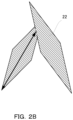
- FIGs. 2A to 2C are schematic views each showing the methods for measuring the length and width of a fissure.
- the length of a fissure 22 corresponds to a length of a line connecting tips in the longitudinal direction of the fissure.
- the width of the fissure 22 corresponds to the maximum length thereof in a direction orthogonal to the longitudinal direction of the fissure (i.e., short direction).
- the width of the fissure 22 is preferably 5 ⁇ m or less. In this case, a risk of direct transmission of light emitted from a light source decreases. Thus, the stress generated by heat accumulated in the phosphor layer can be relaxed, while a risk of impairment of emission characteristics of the phosphor layer decreases.
- the length of the fissure 22 is defined as the length of a line connecting the remaining tip of the fissure 22 to the center of the joining face of the other fissure 22.
- the length of the fissure 22 is defined as the length of a line connecting the center of a line connecting two points of contact between the surface of the phosphor layer and the outer surface of the fissure to the tip of the fissure 22.
- the area ratio of the fissures 22 having a width of 5 mm or less is preferably 5% or more and 10% or less of a vision field of 15 ⁇ m ⁇ 30 ⁇ m in an SEM image observed in any cross-section orthogonal to the substrate 12.
- a vision field 15 ⁇ m ⁇ 30 ⁇ m in an SEM image observed in any cross-section orthogonal to the substrate 12.
- possible cracking of the phosphor layer 14 originating from the fissures 22 and delamination of the phosphor layer 14 from the substrate 12 can be reduced.
- high-energy light emitted from a light source can be employed, while the mechanical strength of the phosphor layer 14 is maintained.
- the area ratio of the fissure 22 tends to increase by elevating the heat elevating rate in the belowmentioned heat treatment step.
- the area ratio of the voids 20 with respect to a vision field of 15 ⁇ m ⁇ 30 ⁇ m in an SEM image observed in any cross-section orthogonal to the substrate 12 is preferably 5% or more and 15% or less, the area of the voids not including the fissures 22 having a width of 5 ⁇ m or less. In this case, even when propagation of the fissures 22 starts by thermal stress generated by heat accumulated in the phosphor layer 14 during irradiation with high-energy light emitted from a light source, propagation of the fissures 22 can be terminated by the voids 20.
- the area ratio of the voids 20 can fall within a specific range by modifying the ratio of a solvent or an inorganic binder added to the phosphor paste.
- the phosphor layer 14 may further contain additional inorganic particles.
- inorganic particles suited for various purposes may be employed. Examples of the purpose include adjusting the viscosity of the phosphor paste, adjusting the phosphor particle density of the phosphor paste, scattering light in the phosphor layer, enhancing thermal conductivity of the phosphor layer, and reducing the number of voids in the phosphor layer.
- the mean particle size of the inorganic particles is preferably equivalent to or smaller than the mean particle size of the phosphor particles contained in the phosphor layer 14.
- the area ratio of voids and that of fissures can be determined through, for example, the following procedure. Firstly, an SEM image is taken in any cross-section orthogonal to the substrate 12 at a magnification of 2,000. Then, the thus-obtained SEM image is subjected to image analysis such as binarization. In this procedure, the image employed for calculating the area ratio is preferably analyzed such that the area ratio values obtained from five vision fields selected at random are averaged so as to cover the entirety of the phosphor layer. Also, a plurality of cross-sectional images (e.g., 5 images) are preferably taken from the phosphor layer.
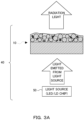
- FIGs. 3A and 3B are schematic views showing a transmission-type light-emitting device and a reflection-type light-emitting device, respectively falling within the scope of the present invention.
- the light-emitting device 40 has a light source 50 and a wavelength-converting member 10.
- the light source 50 is a light-emitting element that can emit light having a specific wavelength from the light source, and an LED, an LD, or the like may be employed. Since the wavelength-converting member 10 achieves efficient wavelength conversion even when a high-power light source is employed, the light source 50 is preferably an LD.
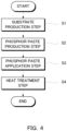
- FIG. 4 is a flowchart showing the method of producing the wavelength-converting member of the present invention. Firstly, a substrate 12 having a specific shape suited for the purpose of use is formed (step S1).
- a phosphor paste is prepared by mixing phosphor particles 16 and an inorganic binder (step S2).
- phosphor particles having a specific mean particle size are provided.
- Various types of the phosphor particles 16 may be used in accordance with designing of the wavelength-converting member 10, and two or more types may be used.
- the thus-provided phosphor particles 16 are weighed, dispersed in a solvent, and mixed with the inorganic binder, to thereby prepare a phosphor paste to be printed.
- the relative amount of a solvent or the inorganic binder added is tuned to adjust the area ratio of voids or fissures to fall within a corresponding range.
- the volume of the binder in the phosphor layer to be formed is tuned to, for example, about 60% or less the phosphor particles, although the ratio varies depending on the type and concentration of the solvent or the inorganic binder.
- the area ratio of the voids or fissures successfully increases.
- Mixing may be conducted by means of a ball mill, a propeller agitator, or the like.
- the mixing time is preferably 3 minutes to 30 minutes.
- propeller agitation the mixing time is preferably 5 minutes to 120 minutes.
- variation in the thickness of the phosphor layer can be reduced.
- the solvent high-boiling-point solvents such as ⁇ -terpineol, butanol, isophoron, and glycerin may be used.
- step S3 onto the surface of the substrate 12 produced in the substrate production step (step S1), the phosphor paste is applied, to thereby form a paste layer (step S3).
- Application of the phosphor paste may be conducted through screen printing, spraying, drawing with a dispenser, or inkjetting. Of these, screen printing is preferred, since a paste layer having a uniform thickness can be consistently formed.
- the thickness of the paste layer is adjusted so as to attain a target thickness after firing.
- the paste layer is preferably formed so as to follow the contour of the substrate 12.
- the heat treatment temperature is preferably 150°C or higher and 300°C or lower, particularly preferably 200°C or higher and 250°C or lower.
- a holding time of 20 minutes or longer is preferably provided.
- the heat treatment time is preferably 0.5 hours or longer and 2.0 hours or shorter.
- the temperature elevation rate is preferably 2°C/min or more, more preferably 2°C/min or more and 10°C/min or less. The temperature elevation rate is appropriately tuned so as to adjust the area ratio of fissures to fall within a specific range.
- an increase in temperature elevation rate results in an increase in the area ratio of fissures, although the effect varies depending on the type and concentration of the solvent or the inorganic binder, the relative amount of addition, and the thickness of the phosphor paste.
- a drying step may be provided before the heat treatment.
- the drying temperature is preferably 100°C or higher and 150°C or lower, and the drying time is more preferably 20 minutes or longer and 60 minutes or shorter.
- a disk-like substrate made of sapphire (diameter ( ⁇ ) 50 mm, thickness (t) 0.5 mm) was provided.
- a YAG-type phosphor (mean particle size: 15 ⁇ m), ⁇ -terpineol (solvent), and ethyl silicate (inorganic binder) were weighed, and the materials were mixed by means of a propeller agitator for 30 minutes, to thereby prepare a phosphor paste.
- the relative amount of the inorganic binder added was tuned by weighing such that the volume of the binder in the phosphor layer to be formed was adjusted to 60% with respect to the amount of the phosphor particles.
- the thus-prepared phosphor paste was applied onto the substrate through screen printing so that the average thickness of the phosphor layer after the heat treatment was adjusted to 50 ⁇ m.
- the coated substrate was dried at 100°C for 20 minutes and then, subjected to a heat treatment in an non-oxidizing atmosphere by means of an electric furnace.
- the heating temperature was elevated to 150°C at a rate of 2°C/min, and the heat treatment was conducted at the temperature for 30 minutes, to thereby fabricate a wavelength-converting member of Example 1-1.
- the area ratio of fissures having a width of 5 ⁇ m or less and the area ratio of the voids (excluding the fissures) in a vision field of 15 ⁇ m ⁇ 30 ⁇ m in an SEM image observed in any cross-section orthogonal to the substrate were determined.
- the area ratio of fissures and the area ratio of the voids (excluding the fissures) were found to be 5% and 10%, respectively.
- Example 1-1 The procedure of Example 1-1 was performed under the same conditions, except that the temperature elevation rate was modified to 5°C/min, to thereby fabricate a wavelength-converting member of Example 1-2.
- the area ratio of fissures and the area ratio of the voids (excluding the fissures) were found to be 7% and 9%, respectively.
- Example 1-1 The procedure of Example 1-1 was performed under the same conditions, except that the temperature elevation rate was modified to 10°C/min, to thereby fabricate a wavelength-converting member of Example 1-3.
- the area ratio of fissures and the area ratio of the voids (excluding the fissures) were found to be 10% and 8%, respectively.
- Example 1-1 The procedure of Example 1-1 was performed under the same conditions, except that the temperature elevation rate was modified to 1.5°C/min for reducing the area ratio of fissures to be smaller than that of Example 1-1, to thereby fabricate a wavelength-converting member of Example 1-4.
- the area ratio of fissures and the area ratio of the voids (excluding the fissures) were found to be 3% and 10%, respectively.
- Example 1-1 The procedure of Example 1-1 was performed under the same conditions, except that the temperature elevation rate was modified to 12°C/min for elevating the area ratio of fissures to be greater than that of Example 1-3, to thereby fabricate a wavelength-converting member of Example 1-5.
- the area ratio of fissures and the area ratio of the voids (excluding the fissures) were found to be 12% and 8%, respectively.
- Example 1-1 The procedure of Example 1-1 was performed under the same conditions, except that the relative amount of the inorganic binder to be added was changed to 90% for adjusting the area ratio of the voids (excluding the fissures) to be smaller than that of Example 1-1, to thereby fabricate a wavelength-converting member of Example 2-1.
- the area ratio of fissures and the area ratio of the voids (excluding the fissures) were found to be 5% and 3%, respectively.
- Example 1-1 The procedure of Example 1-1 was performed under the same conditions, except that the relative amount of the inorganic binder to be added was changed to 50% for adjusting the area ratio of the voids (excluding the fissures) to be greater than that of Example 1-1, to thereby fabricate a wavelength-converting member of Example 2-2.
- the area ratio of fissures and the area ratio of the voids (excluding the fissures) were found to be 5% and 18%, respectively.
- Each of the above-produced wavelength-converting members was irradiated with light emitted from a light source at different levels A to C for 60 minutes. Delamination of a phosphor layer was checked. The light emitted from the light source, which was a blue LD, had a wavelength of 450 nm. The output levels were 0.5 W (level A), 1.0 W (level B), and 2.0 W (level C). Irradiation was conducted from the weak level to the strong level in laser light output. At the timing when delamination occurred, the test of the phosphor layer in the trial was finished.
- Example 1-5 the phosphor layer was partially defoliated through irradiation with light emitted from a light source at a level B.
- the strength of the phosphor layer itself decreased, to thereby cause delamination of the phosphor layer by high-energy light emitted from a light source.
- Example 1-1 to 1-3 and 2-2 no delamination of the phosphor layer occurred through irradiation with light emitted from a light source at a level C.
- the phosphor layer was partially defoliated through irradiation with light emitted from a light source at a level C.
- the area ratio of fissures was low in Example 1-4, delamination of the phosphor layer occurred from a part where sufficient relaxation of thermal stress by fissures was not achieved at a higher output of light emitted from a light source.
- Example 2-1 since the area ratio of voids was low in Example 2-1, delamination of the phosphor layer occurred as a result of propagation of fissures in a part having few voids at a higher output of light emitted from a light source.
- the wavelength-converting member 10 was irradiated with blue LD laser (wavelength: 450 nm) as laser light with an output of 0.5 W.
- the chromaticity of light transmitted to the face opposite the incident side face was determined by means of a spectroradiometer (CL-500A, product of Konica Minolta, Inc.). In each Example, chromaticity was measured at 5 points, and the values were averaged.
- Chromaticity is defined as a numerical index for color characteristics including hue, chroma, and brightness (but excluding brightness).
- chromaticity is represented by an international representation defined by Commission Internationale de l'Eclairage (CIE) in 1931, with a combination of (x,y) according to an X-Y chromaticity chart based on the CIE-XYZ color system.
- CIE Commission Internationale de l'Eclairage
- X-Y chromaticity chart the greater the x-axis value, the greater the ratio of "red” sense.
- the smaller the x-axis value the greater the ratio of "blue” sense.
- the greater the y-axis value the greater the ratio of "green” sense.
- the smaller the y-axis value the greater the ratio of "blue” sense.
- the maximum value and average value of the deviation of chromaticity measurements in the X-axis direction were calculated.
- the score was "good.”
- the score was "excellent emission performance.”
- the maximum value of the deviation in the X-axis direction was 10% or less the average value of the deviation in the X-axis direction. Also, in Examples 1-1 to 1-5 and 2-1, the maximum value of the deviation in the X-axis direction was 5% or less the average value of the deviation in the X-axis direction. Conceivably, since the area ratio of voids was high in Example 2-2, break-through of light emitted from a light source increased as compared with the other Examples, resulting in intense blue sensation.
- thermal stress generated by heat accumulated in the phosphor layer during irradiation with high-energy light emitted from a light source was conceived to be relaxed by voids and fissures, to thereby provide excellent durability to against higher-energy light emitted from a light source.
- possible adverse effect on the light-emission characteristics of the phosphor layer was found to be reduced by voids and fissures, to thereby relax the stress generated by heat accumulated in the phosphor layer.
Landscapes
- Engineering & Computer Science (AREA)
- Physics & Mathematics (AREA)
- General Engineering & Computer Science (AREA)
- Spectroscopy & Molecular Physics (AREA)
- Optics & Photonics (AREA)
- Chemical & Material Sciences (AREA)
- Electromagnetism (AREA)
- Condensed Matter Physics & Semiconductors (AREA)
- General Physics & Mathematics (AREA)
- Microelectronics & Electronic Packaging (AREA)
- Organic Chemistry (AREA)
- Materials Engineering (AREA)
- Luminescent Compositions (AREA)
- Led Device Packages (AREA)
- Optical Filters (AREA)
Applications Claiming Priority (2)
| Application Number | Priority Date | Filing Date | Title |
|---|---|---|---|
| JP2022027809A JP7773923B2 (ja) | 2022-02-25 | 2022-02-25 | 波長変換部材、および発光装置 |
| PCT/JP2022/047270 WO2023162445A1 (ja) | 2022-02-25 | 2022-12-22 | 波長変換部材、および発光装置 |
Publications (2)
| Publication Number | Publication Date |
|---|---|
| EP4485017A1 true EP4485017A1 (de) | 2025-01-01 |
| EP4485017A4 EP4485017A4 (de) | 2026-03-04 |
Family
ID=87765594
Family Applications (1)
| Application Number | Title | Priority Date | Filing Date |
|---|---|---|---|
| EP22928962.4A Pending EP4485017A4 (de) | 2022-02-25 | 2022-12-22 | Wellenlängenumwandlungselement und lichtemittierende vorrichtung |
Country Status (6)
| Country | Link |
|---|---|
| EP (1) | EP4485017A4 (de) |
| JP (1) | JP7773923B2 (de) |
| KR (1) | KR20240158273A (de) |
| CN (1) | CN118715401A (de) |
| TW (1) | TW202335321A (de) |
| WO (1) | WO2023162445A1 (de) |
Family Cites Families (5)
| Publication number | Priority date | Publication date | Assignee | Title |
|---|---|---|---|---|
| JP2015038960A (ja) | 2013-05-16 | 2015-02-26 | 株式会社日本セラテック | 発光装置 |
| CN108369982A (zh) * | 2015-12-11 | 2018-08-03 | 松下知识产权经营株式会社 | 波长转换体、波长转换构件及发光装置 |
| JP7019496B2 (ja) * | 2017-04-11 | 2022-02-15 | 日本特殊陶業株式会社 | 波長変換部材およびその製造方法 |
| CN114766009A (zh) * | 2019-12-04 | 2022-07-19 | 夏普株式会社 | 波长转换元件、波长转换装置及发光系统 |
| JP2023058756A (ja) * | 2020-03-10 | 2023-04-26 | シャープ株式会社 | 光学素子および発光システム |
-
2022
- 2022-02-25 JP JP2022027809A patent/JP7773923B2/ja active Active
- 2022-12-07 TW TW111146897A patent/TW202335321A/zh unknown
- 2022-12-22 EP EP22928962.4A patent/EP4485017A4/de active Pending
- 2022-12-22 KR KR1020247032004A patent/KR20240158273A/ko active Pending
- 2022-12-22 CN CN202280091919.9A patent/CN118715401A/zh active Pending
- 2022-12-22 WO PCT/JP2022/047270 patent/WO2023162445A1/ja not_active Ceased
Also Published As
| Publication number | Publication date |
|---|---|
| KR20240158273A (ko) | 2024-11-04 |
| JP7773923B2 (ja) | 2025-11-20 |
| TW202335321A (zh) | 2023-09-01 |
| CN118715401A (zh) | 2024-09-27 |
| JP2023124190A (ja) | 2023-09-06 |
| EP4485017A4 (de) | 2026-03-04 |
| WO2023162445A1 (ja) | 2023-08-31 |
Similar Documents
| Publication | Publication Date | Title |
|---|---|---|
| EP3451031B1 (de) | Wellenlängenumwandlungselement, herstellungsverfahren dafür und lichtemittierende vorrichtung | |
| EP3407101B1 (de) | Wellenlängenumwandlungselement und lichtemittierende vorrichtung | |
| JP2014241431A (ja) | 発光装置の製造方法 | |
| JP6516271B2 (ja) | 波長変換部材および発光装置 | |
| JP7019496B2 (ja) | 波長変換部材およびその製造方法 | |
| US11060020B2 (en) | Wavelength conversion member | |
| EP4485017A1 (de) | Wellenlängenumwandlungselement und lichtemittierende vorrichtung | |
| JP6934316B2 (ja) | 波長変換部材 | |
| JP7685454B2 (ja) | 波長変換部材、その製造方法、および発光装置 | |
| JP6775429B2 (ja) | 波長変換部材の製造方法 | |
| JP7833380B2 (ja) | 波長変換部材、その製造方法、および発光装置 | |
| JP2025088371A (ja) | 波長変換部材、および発光装置 | |
| JP2021099415A (ja) | 波長変換部材および発光装置 | |
| JP7519743B2 (ja) | 波長変換部材および発光装置 | |
| JP2024083805A (ja) | 波長変換部材、その製造方法、および発光装置 |
Legal Events
| Date | Code | Title | Description |
|---|---|---|---|
| STAA | Information on the status of an ep patent application or granted ep patent |
Free format text: STATUS: THE INTERNATIONAL PUBLICATION HAS BEEN MADE |
|
| PUAI | Public reference made under article 153(3) epc to a published international application that has entered the european phase |
Free format text: ORIGINAL CODE: 0009012 |
|
| STAA | Information on the status of an ep patent application or granted ep patent |
Free format text: STATUS: REQUEST FOR EXAMINATION WAS MADE |
|
| 17P | Request for examination filed |
Effective date: 20240906 |
|
| AK | Designated contracting states |
Kind code of ref document: A1 Designated state(s): AL AT BE BG CH CY CZ DE DK EE ES FI FR GB GR HR HU IE IS IT LI LT LU LV MC ME MK MT NL NO PL PT RO RS SE SI SK SM TR |
|
| DAV | Request for validation of the european patent (deleted) | ||
| DAX | Request for extension of the european patent (deleted) | ||
| A4 | Supplementary search report drawn up and despatched |
Effective date: 20260204 |
|
| RIC1 | Information provided on ipc code assigned before grant |
Ipc: G02B 5/20 20060101AFI20260129BHEP Ipc: F21S 2/00 20160101ALI20260129BHEP Ipc: F21V 7/30 20180101ALI20260129BHEP Ipc: F21V 9/35 20180101ALI20260129BHEP Ipc: F21Y 115/10 20160101ALI20260129BHEP Ipc: F21Y 115/30 20160101ALI20260129BHEP |