EP4468043A1 - Beugungsgitter und form zur herstellung eines beugungsgitters - Google Patents
Beugungsgitter und form zur herstellung eines beugungsgitters Download PDFInfo
- Publication number
- EP4468043A1 EP4468043A1 EP23743267.9A EP23743267A EP4468043A1 EP 4468043 A1 EP4468043 A1 EP 4468043A1 EP 23743267 A EP23743267 A EP 23743267A EP 4468043 A1 EP4468043 A1 EP 4468043A1
- Authority
- EP
- European Patent Office
- Prior art keywords
- diffraction grating
- grating
- height
- steps
- pattern
- Prior art date
- Legal status (The legal status is an assumption and is not a legal conclusion. Google has not performed a legal analysis and makes no representation as to the accuracy of the status listed.)
- Pending
Links
Images




Classifications
-
- G—PHYSICS
- G02—OPTICS
- G02B—OPTICAL ELEMENTS, SYSTEMS OR APPARATUS
- G02B5/00—Optical elements other than lenses
- G02B5/18—Diffraction gratings
- G02B5/1814—Diffraction gratings structurally combined with one or more further optical elements, e.g. lenses, mirrors, prisms or other diffraction gratings
- G02B5/1819—Plural gratings positioned on the same surface, e.g. array of gratings
- G02B5/1823—Plural gratings positioned on the same surface, e.g. array of gratings in an overlapping or superposed manner
-
- G—PHYSICS
- G02—OPTICS
- G02B—OPTICAL ELEMENTS, SYSTEMS OR APPARATUS
- G02B5/00—Optical elements other than lenses
- G02B5/18—Diffraction gratings
- G02B5/1814—Diffraction gratings structurally combined with one or more further optical elements, e.g. lenses, mirrors, prisms or other diffraction gratings
- G02B5/1819—Plural gratings positioned on the same surface, e.g. array of gratings
-
- G—PHYSICS
- G02—OPTICS
- G02B—OPTICAL ELEMENTS, SYSTEMS OR APPARATUS
- G02B5/00—Optical elements other than lenses
- G02B5/18—Diffraction gratings
- G02B5/1847—Manufacturing methods
- G02B5/1852—Manufacturing methods using mechanical means, e.g. ruling with diamond tool, moulding
-
- G—PHYSICS
- G02—OPTICS
- G02B—OPTICAL ELEMENTS, SYSTEMS OR APPARATUS
- G02B5/00—Optical elements other than lenses
- G02B5/18—Diffraction gratings
- G02B5/1876—Diffractive Fresnel lenses; Zone plates; Kinoforms
-
- G—PHYSICS
- G02—OPTICS
- G02B—OPTICAL ELEMENTS, SYSTEMS OR APPARATUS
- G02B5/00—Optical elements other than lenses
- G02B5/18—Diffraction gratings
- G02B5/1866—Transmission gratings characterised by their structure, e.g. step profile, contours of substrate or grooves, pitch variations, materials
Definitions
- the present disclosure relates to a diffraction grating and a mold for forming a diffraction grating.
- a diffraction grating with a step-like cross-sectional shape As a diffraction grating, a diffraction grating with a step-like cross-sectional shape has been known.
- a diffraction grating with a step-like cross-sectional shape of the Nth power of 2 steps is formed by repeating lithography and etching for N times. Also, when plural types of diffraction grating portions with different grating periods are formed, the diffraction grating portion with short grating period is formed in smaller number of steps than the diffraction grating portion with long grating period, in view of manufacturing limitations. This method is described, for example, in Non-Patent Document 1.
- the diffraction efficiency of the diffraction grating portion with short grating period decreases since the number of steps is decreased.
- the grating height of the diffraction grating portion with short grating period may be lower than that of the diffraction grating portion with long grating period, depending on, for example, the characteristics of the etching device and the etching conditions. Similarly, in such a case, the grating height may be uneven, and the diffraction efficiency decreases.
- Patent Document 1 and Patent Document 2 disclose a method wherein an etching stopper layer is placed for each step.
- this method since it is necessary to form an etching stopper layer in advance for each step, the production process gets more complicated and requires a longer time.
- Non-Patent Document 1 Zhiyu Zhang and et al., "Hybrid-level Fresnel zone plate for diffraction efficiency enhancement" Optics Express Vol. 25, Issue 26, pp. 33676-33687 (2017 )
- the present disclosure has been made in view of the above circumstances, and a main object of the present disclosure is to provide a diffraction grating capable of improving the evenness of the grating height without using an etching stopper layer.
- a diffraction grating comprising: an optically transparent substrate; and a diffraction grating structure, with a step-like cross-sectional shape, on a surface of the optically transparent substrate, wherein the diffraction grating structure is formed of a single member, the diffraction grating structure includes a first diffraction grating portion and a second diffraction grating portion with different grating periods and different numbers of steps, a grating period of the second diffraction grating portion is shorter than a grating period of the first diffraction grating portion, a number of steps of the second diffraction grating portion is more than a number of steps of the first diffraction grating portion, and a difference between a grating height of the first diffraction grating portion and a grating height of the second diffraction grating portion is less than a minimum height of one step of the first diffraction
- the difference between the grating height of the first diffraction grating portion and the grating height of the second diffraction grating portion is preferably 15% or less with respect to 100% of the grating height of the first diffraction grating portion.
- the number of steps of the first diffraction grating portion is preferably 7 or more.
- One embodiment of the present disclosure provides a mold for forming a diffraction grating comprising a pattern structure configured to duplicate the diffraction grating described above.
- One embodiment of the present disclosure provides a mold for forming a diffraction grating comprising: an optically transparent substrate; and a pattern structure, with a step-like cross-sectional shape, on a surface of the optically transparent substrate, wherein the pattern structure is formed of a single member, the pattern structure includes a first pattern portion and a second pattern portion with different pattern periods and different numbers of steps, a pattern period of the second pattern portion is shorter than a pattern period of the first pattern portion, a number of steps of the second pattern portion is more than a number of steps of the first pattern portion, and a difference between a pattern height of the first pattern portion and a pattern height of the second pattern portion is less than a minimum height of one step of the first pattern portion.
- the difference between the pattern height of the first pattern portion and the pattern height of the second pattern portion is preferably 15% or less with respect to 100% of the pattern height of the first pattern portion.
- the number of steps of the first pattern portion is preferably 7 or more.
- One embodiment of the present disclosure provides a diffraction grating comprising a diffraction grating structure duplicated by the mold for forming a diffraction grating described above.
- the diffraction grating in the present disclosure exhibits an effect of improving the evenness of the grating height, and improving diffraction efficiency.
- the diffraction grating in the present disclosure is hereinafter described.
- the diffraction grating in the present disclosure comprises: a diffraction grating structure, with a step-like cross-sectional shape, on a surface of an optically transparent substrate, wherein the diffraction grating structure is formed of a single member; the diffraction grating structure includes a first diffraction grating portion and a second diffraction grating portion with different grating periods and different numbers of steps; a grating period of the second diffraction grating portion is shorter than a grating period of the first diffraction grating portion; a number of steps of the second diffraction grating portion is more than a number of steps of the first diffraction grating portion; and a difference between a grating height of the first diffraction grating portion and a grating height of the second diffraction grating portion is less than a minimum height of one step of the first diffraction grating portion.
- FIG. 1 is a schematic cross-sectional view illustrating an example of a diffraction grating in the present disclosure.
- a diffraction grating 1 in FIG. 1 comprises a diffraction grating structure 3, with a step-like cross-sectional shape, on the surface of an optically transparent substrate 2.
- the step-like shape is a shape with a number of steps of two steps or more.
- the diffraction grating structure 3 is formed of a single member, and includes a first diffraction grating portion 4 and a second diffraction grating portion 5 with different grating periods and numbers of steps.
- the grating period P2 of the second diffraction grating portion 5 is shorter than the grating period P1 of the first diffraction grating portion 4. Also, the number of steps of the second diffraction grating portion 5 is more than the number of steps of the first diffraction grating portion 4. For example, in FIG. 1 , the number of steps of the first diffraction grating portion 4 is eight steps, and the number of steps of the second diffraction grating portion 5 is nine steps.
- the difference between the grating height H1 of the first diffraction grating portion 4 and the grating height H2 of the second diffraction grating portion 5 is less than the minimum height D1 of one step of the first diffraction grating portion 4.
- the minimum height D1 of one step of the first diffraction grating portion 4 is the minimum height among the heights of the steps of the first diffraction grating portion 4.
- FIG. 1 shows the case where the height of one step of the first diffraction grating portion 4 is the same for all steps. In this case, the height of every one step of the first diffraction grating portion 4 is the minimum height D1. That is, the minimum height D1 of one step of the first diffraction grating portion 4 may be the height of one step of the first diffraction grating portion 4. In FIG. 1 , for example, the height of one step of the lowest step of the first diffraction grating portion 4 is regarded as the minimum height D1.
- FIGS. 2A to 2J and FIGS. 3A and 3B are process drawings illustrating an example of a conventional method for producing a diffraction grating.
- a resist layer 103a is formed on a substrate 102, and a pattern exposure is carried out by irradiating energy rays 105 such as ultraviolet rays via a mask 104.
- a resist pattern 103b is formed.
- FIG. 2A a resist layer 103a is formed on a substrate 102, and a pattern exposure is carried out by irradiating energy rays 105 such as ultraviolet rays via a mask 104.
- a resist pattern 103b is formed.
- FIG. 1 As shown in FIG.
- the substrate 102 is etched.
- the resist pattern 103b is removed. Thereby, a step-like shape with 2 steps is formed.
- the formation of the resist layer 103a, the pattern exposure, the etching of the substrate 102, and the removal of the resist pattern 103b are further carried out to form a step-like shape with 4 steps.
- the formation of the resist layer 103a, the pattern exposure, the etching of the substrate 102, and the removal of the resist pattern 103b are further carried out to form a step-like shape with 8 steps.
- a diffraction grating structure with a step-like shape with the 3rd power of 2, that is, 8 steps may be formed.
- the diffraction grating portion with short grating period is formed in smaller number of steps than the diffraction grating portion with long grating period, in view of manufacturing limitations.
- the number of steps of the diffraction grating portion with short grating period is, for example, the (N-1)th power of 2.
- the number of steps of the diffraction grating portion 111 with long grating period is the 3rd power of 2, that is, 8 steps
- the number of steps of the diffraction grating portion 112 with short grating period is the 2nd power of 2, that is, 4 steps.
- the number of steps of the diffraction grating portion 111 with long grating period is 16 steps (the 4th power of 2)
- the number of steps of the diffraction grating portion 112 with short grating period is the 3rd power of 2, that is, 8 steps.
- the grating height h2 of the diffraction grating portion 112 with a short grating period is lower than the grating height h1 of the diffraction grating portion 111 with long grating period by the height d1 of one step of the diffraction grating portion 111 with long grating period. Therefore, in the diffraction grating portion 112 with short grating period, since the number of steps is reduced, the diffraction efficiency is reduced.
- the grating height of the diffraction grating portion with short grating period may be lower than that of the diffraction grating portion with long grating period, depending on, for example, the characteristics of the etching device and the etching conditions. In such a case, the grating height may be uneven, and the diffraction efficiency decreases.
- the grating period of the second diffraction grating portion is shorter than the grating period of the first diffraction grating portion, the number of steps of the second diffraction grating portion is more than the number of steps of the first diffraction grating portion.
- the difference between the grating height of the first diffraction grating portion and the grating height of the second diffraction grating portion may be made less than the minimum height of one step of the first diffraction grating portion, and the grating height may be made even. Therefore, the diffraction efficiency may be improved.
- the diffraction grating in the present disclosure comprises a diffraction grating structure, with a step-like cross-sectional shape, on a surface of an optically transparent substrate.
- the diffraction grating structure includes a first diffraction grating portion and a second diffraction grating portion with different grating periods and numbers of steps; the grating period of the second diffraction grating portion is shorter than the grating period of the first diffraction grating portion; the number of steps of the second diffraction grating portion is more than the number of steps of the first diffraction grating portion; and a difference between a grating height of the first diffraction grating portion and a grating height of the second diffraction grating portion is less than a minimum height of one step of the first diffraction grating portion.
- the difference between the grating height of the first diffraction grating portion and the grating height of the second diffraction grating portion is preferably, for example, 15% or less, more preferably 9% or less, and further preferably 6% or less, with respect to 100% of the grating height of the first diffraction grating portion.
- the difference described above is 15% or less, the uniformity of the grating height of the diffraction grating structure may be improved so that the diffraction efficiency may be improved.
- the difference described above is 9% or less, or 6% or less, the diffraction efficiency may further be improved.
- the grating height of the first diffraction grating portion is set appropriately according to the use application of the diffraction grating. In general, when the height of one step is the same for all steps, the height may be set to the grating height H1 determined from the following formulas (1) and (2).
- H1 D1 ⁇ (L - 1)
- D1 2 ⁇ ⁇ / ( L ⁇ 2 ⁇ ⁇ n)
- the grating height H1 is 1645 nm.
- the grating height of the second diffraction grating portion may be similar to the grating height of the first diffraction grating portion described above.
- the grating height of the second diffraction grating portion may be higher than, or lower than the grating height of the first diffraction grating portion, and may be the same as the grating height of the first diffraction grating portion.
- the height of one step of the second diffraction grating portion is lower than the height of one step of the first diffraction grating portion.
- the number of steps of the second diffraction grating portion is nine, and the heights D2a of the first step to eighth step are the same.
- the height D2b of the ninth step is lower than the heights D2a of the first step to the eighth step.
- the height D2b of the ninth step is higher than the heights D2a of the first step to the eighth step.
- the grating period of the second diffraction grating portion is shorter than the grating period of the first diffraction grating portion.
- the difference between the grating period of the first diffraction grating portion and the grating period of the second diffraction grating portion is not particularly limited as long as the grating period of the second diffraction grating portion is shorter than the grating period of the first diffraction grating portion, and is set appropriately according to the use application of the diffraction grating.
- the production of the diffraction grating may be difficult in view of manufacturing limitations.
- the grating period of the second diffraction grating portion has only to be shorter than the grating period of the first diffraction grating portion described above.
- the production of the diffraction grating may be difficult in view of manufacturing limitations.
- the grating period of each diffraction grating portion is the distance from the outer end point of the top portion surface to the outer end point of the bottom portion surface in the surface direction of the diffraction grating.
- the grating height P1 of the first diffraction grating portion 4 is the distance from the outer end point of the top portion surface to the outer end point of the bottom portion surface of the first diffraction grating portion 4; and the grating height P2 of the second diffraction grating portion 5 is the distance from the outer end point of the top portion surface to the outer end point of the bottom portion surface of the second diffraction grating portion 5.
- the grating period is regarded as P1, P2, and P.
- the period is not considered as a grating period.
- the width of one step of the first diffraction grating portion and the second diffraction grating portion is respectively set appropriately according to the grating period, and number of steps of the first diffraction grating portion and the second diffraction grating portion.
- the width of one step is too short, the production of the diffraction grating may be difficult in view of manufacturing limitations.
- the width of one step of the second diffraction grating portion is usually less than the width of one step of the first diffraction grating portion.
- the width of one step may be, for example, the same for all steps, and may be different for each step.
- the number of steps of the second diffraction grating portion is more than the number of steps of the first diffraction grating portion.
- the difference between the number of steps of the first diffraction grating portion and the number of steps of the second diffraction grating portion is not particularly limited as long as the number of steps of the second diffraction grating portion is more than the number of steps of the first diffraction grating portion, and may be, for example, 1 or more, and may be 1 or more and 4 or less.
- the difference between the number of steps of the first diffraction grating portion and the number of steps of the second diffraction grating portion is usually 1.
- the number of steps of the first diffraction grating portion and the second diffraction grating portion is preferably, for example, 7 or more, more preferably 12 or more, and further preferably 16 or more.
- the number of steps is 7 or more, the diffraction efficiency may be improved.
- the number of steps is 12 or more, or 16 or more, the diffraction efficiency may further be improved. Meanwhile, there is a limit to the effect of improving diffraction efficiency by increasing the number of steps.
- the number of steps of the first diffraction grating portion and the second diffraction grating portion is preferably, for example, 16 or less, from the viewpoint of the number of processing steps.
- the number of steps of each diffraction grating portion is the number of planes parallel to the surface of the optically transparent substrate in each diffraction grating portion.
- the number of steps of the first diffraction grating portion 4 is eight, and the number of steps of the second diffraction grating portion 5 is nine.
- the diffraction grating structure has only to include at least a first diffraction grating portion and a second diffraction grating portion with different grating periods and numbers of steps.
- the diffraction grating structure may include plural types of the first diffraction grating portions with same number of steps and different grating periods.
- the grating period of the second diffraction grating portion is shorter than the grating period of all the first diffraction grating portions, and the number of steps of the second diffraction grating portion is more than the number of steps of all the first diffraction grating portions. For example, in FIG.
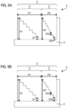
- the diffraction grating structure 3 includes plural types of the first diffraction grating portions 4a, 4b with the same number of steps of 8 steps and different grating periods P1a, P1b.
- the diffraction grating structure 3 includes plural types of the first diffraction grating portions 4a, 4b, 4c with the same number of steps of 8 steps and different grating periods P1a, P1b, P1c.
- the design values for the grating heights H1a, H1b, or H1a, H1b, H1c for each first diffraction grating portion 4a, 4b or 4a, 4b, 4c are usually the same value.
- FIG. 8B is a cross-sectional view of FIG. 8A , and is an example wherein the diffraction grating is a diffraction type Fresnel lens.
- the diffraction grating structure includes, as the first diffraction grating portion, plural types of the first diffraction grating portions with the same number of steps and different grating periods, the number of types of the first diffraction grating portion is not particularly limited as long as it is two or more, and is selected appropriately according to the use application of the diffraction grating.
- the diffraction grating structure may include plural types of the second diffraction grating portions with the same or different numbers of steps and different grating periods.
- the grating periods of all the second diffraction grating portions are shorter than the grating periods of the first diffraction grating portions, and the numbers of steps of all the second diffraction grating portions are more than the numbers of steps of the first diffraction grating portions. For example, in FIG.
- the diffraction grating structure 3 includes plural types of the second diffraction grating portions 5a, 5b with the same number of steps of 9 steps and different grating periods P2a, P2b.
- the grating height H2a, H2b of each second diffraction grating portion 5a, 5b may or may not be the same, as long as the difference between the grating height H1 of the first diffraction grating portion 4 and the grating height H2a, H2b of each second diffraction grating portion 5a, 5b is respectively in a predetermined range.
- the diffraction grating structure includes, as the second diffraction grating portion, plural types of the second diffraction grating portions with the same or different numbers of steps and different grating periods, the number of types of the second diffraction grating portions is not particularly limited as long as it is two or more, and is usually 2 or more and 4 or less.
- the diffraction grating structure has a step-like cross-sectional shape.
- the diffraction grating structure may be an approximation of a slope to the step-like shape.
- the diffraction grating structure may be, for example, an approximation of a smooth surface to the step-like shape, and may be an approximation of a curved surface to the step-like shape.
- the diffraction grating structure is formed of a single member, that is, one member. Therefore, the diffraction grating structure is not formed of multiple members as a conventional structure including an etching stopper layer.
- the diffraction grating in the present disclosure is not particularly limited as long as the diffraction grating structure is formed of a single member, and the optically transparent substrate and the diffraction grating structure may be integrated, and may be separate members.
- the optically transparent substrate and the diffraction grating structure being integrated means that the optically transparent substrate and the diffraction grating structure are constituted with one layer.
- the diffraction grating may include an optically transparent substrate, and an optically transparent layer, placed on one surface of the optically transparent substrate, constituting a diffraction grating structure.
- the optically transparent substrate is not particularly limited as long as it has transparency to the light of the objective wavelength.
- the material of the optically transparent substrate capable of transmitting visible light may be, for example, glass, quartz, and resin.
- the material of the optically transparent substrate capable of transmitting infrared light may be, for example, silicon.
- the optically transparent layer is not particularly limited as long as it has transparency to the light of the objective wavelength.
- the material of the optically transparent layer capable of transmitting visible light may be, for example, silicon oxide, silicon nitride, silicon oxide/nitride, and resin.
- the resin may include ultraviolet curable resins, thermosetting resins, electron beam curable resins, and spin-on glass of ultraviolet curable type or thermosetting type.
- the ultraviolet curable resin may include resins including, for example, urethane acrylate, polyester acrylate, epoxy acrylate, polyether acrylate, polythiol, or butadiene acrylate as a main component.
- a cohesiveness layer may be formed between the optically transparent substrate and the optically transparent layer.
- the cohesiveness layer may be, for example, a silane coupling agent.
- close adhesiveness between the optically transparent substrate and the optically transparent layer may be improved.
- the optically transparent substrate and the optically transparent layer may be suppressed from being peeled off in the imprinting method. Further, when used as a diffraction grating for a long time, improved close adhesiveness is often advantageous.
- the diffraction grating in the present disclosure may be, for example, a transmission type diffraction grating.
- the diffraction grating in the present disclosure is preferably, for example, a diffraction type Fresnel lens.
- a diffraction type Fresnel lens As shown in FIGS. 8A and 8B for example, in the diffraction type Fresnel lens, the grating period of the diffraction grating portion is shortened from the center to the outer periphery. For this reason, the diffraction grating portion at the outer periphery portion of a conventional diffraction type Fresnel lens is formed by reducing the number of steps, from the viewpoint of manufacturing limitations.
- the grating height is reduced as described above.
- the diffraction type Fresnel lens is also called a harmonic Fresnel lens, for example.
- the diffraction grating structure in the present disclosure described above may also be used as a pattern structure for a mold for forming a diffraction grating in the imprinting method.
- each term is read as follows.
- the diffraction grating structure is read in a different way as pattern structure.
- the diffraction grating is read in a different way as mold for forming a diffraction grating.
- the grating period is read in a different way as pattern period.
- the first diffraction grating portion is read in a different way as first pattern portion.
- the second diffraction grating portion is read in a different way as second pattern portion.
- the grating height is read in a different way as pattern height.
- the mold for forming a diffraction grating in the present disclosure comprises a pattern structure, with a step-like cross-sectional shape, on a surface of an optically transparent substrate, wherein the pattern structure is formed of a single member; the pattern structure includes a first pattern portion and a second pattern portion with different pattern periods and different numbers of steps; a pattern period of the second pattern portion is shorter than a pattern period of the first pattern portion; a number of steps of the second pattern portion is more than a number of steps of the first pattern portion; and a difference between a pattern height of the first pattern portion and a pattern height of the second pattern portion is less than a minimum height of one step of the first pattern portion.
- the pattern structure includes a first pattern portion and a second pattern portion with different pattern periods and numbers of steps; the pattern period of the second pattern portion is shorter than the pattern period of the first pattern portion; the number of steps of the second pattern portion is more than the number of steps of the first pattern portion; and a difference between a pattern height of the first pattern portion and a pattern height of the second pattern portion is less than a minimum height of one step of the first pattern portion.
- the difference between the pattern height of the first pattern portion and the pattern height of the second pattern portion is less than a minimum height of one step of the first pattern portion.
- the difference between the pattern height of the first pattern portion and the pattern height of the second pattern portion is preferably, for example, 15% or less, more preferably 9% or less, and further preferably 6% or less, with respect to 100% of the pattern height of the first pattern portion.
- the difference described above is 15% or less, in the diffraction grating formed by the imprinting method, the uniformity of the grating height of the diffraction grating structure may be improved so that the diffraction efficiency may be improved.
- the difference described above is 9% or less, or 6% or less, the diffraction efficiency in the diffraction grating formed by the imprinting method may further be improved.
- the number of steps of the first pattern portion and the second pattern portion is preferably, for example, 7 or more, more preferably 12 or more, and further preferably 16 or more, respectively.
- the number of steps is 7 or more, the diffraction efficiency in the diffraction grating formed by the imprinting method may be improved.
- the number of steps is 12 or more, or 16 or more, the diffraction efficiency in the diffraction grating formed by the imprinting method may further be improved. Meanwhile, there is a limit to the effect of improving diffraction efficiency by increasing the number of steps.
- the number of steps of the first pattern portion and the second pattern portion is preferably, for example, 16 or less respectively, from the viewpoint of the number of processing steps.
- the optically transparent substrate and the pattern structure may be integrated, and may be separate members. Examples of the embodiment wherein the optically transparent substrate and the pattern structure are integrated, may include a master mold. Examples pf the embodiment wherein the optically transparent substrate and the pattern structure are separate members, may include a replica mold.
- the method for producing a diffraction grating in the present disclosure is not particularly limited as long as it is capable of producing a diffraction grating including the diffraction grating structure described above on the surface of an optically transparent substrate, and a method wherein each step is formed by repeating lithography and etching, is preferable.
- FIGS. 9A to 9J and FIGS. 10A and 10F are process drawings illustrating an example of a method for producing a diffraction grating in the present disclosure.
- a resist layer 11a is formed on an optically transparent substrate 2, and a pattern exposure is carried out by irradiating energy rays 13 such as ultraviolet rays via a mask 12.
- a resist pattern 11b is formed.
- the optically transparent substrate 2 is etched.
- the resist pattern 11b is removed. Thereby, the first step is formed.
- FIGS. 9A to 9J and FIGS. 10A and 10F are process drawings illustrating an example of a method for producing a diffraction grating in the present disclosure.
- FIG. 9A a resist layer 11a is formed on an optically transparent substrate 2, and a pattern exposure is carried out by irradiating energy rays 13 such as ultraviolet rays via a mask 12.
- a resist pattern 11b is formed.
- the optically transparent substrate 2 is etched.
- the formation of the resist layer 11a, the pattern exposure, the etching of the optically transparent substrate 2, and the removal of the resist pattern 11b are further carried out.
- the second step is formed.
- the formation of the resist layer 11a, the pattern exposure, the etching of the optically transparent substrate 2, and the removal of the resist pattern 11b are carried out repeatedly.
- the third to seventh steps are formed.
- FIGS. 9I to 9J and FIGS. 10A to 10B the formation of the resist layer 11a, the pattern exposure, the etching of the optically transparent substrate 2, and the removal of the resist pattern 11b are further carried out.
- the eighth step is formed, and the first diffraction grating portion 4 is formed.
- the formation of the resist layer 11a, the pattern exposure, the etching of the optically transparent substrate 2, and the removal of the resist pattern 11b are further carried out.
- the ninth step is formed, and the second diffraction grating portion 5 is formed.
- a diffraction grating structure including the first diffraction grating portion with N steps, and the second diffraction grating portion with (N + 1) steps may be formed.
- the difference between the grating height of the first diffraction grating portion and the grating height of the second diffraction grating portion may be made less than the minimum height of one step of the first diffraction grating portion, by etching the optically transparent substrate so that the difference of the grating height of the obtained second diffraction grating portion with respect to the grating height of the first diffraction grating portion is less than the minimum height of one step of the first diffraction grating portion.
- a diffraction grating for example, by forming a diffraction grating structure on the surface of an optically transparent substrate in advance, a diffraction grating portion wherein the difference with respect to the grating height of the first diffraction grating portion is the minimum height, of one step of the first diffraction grating portion, or more (Hereinafter, it may be referred to as a specific diffraction grating portion, in some cases.) may be specified, and the specific diffraction grating portion may be designed.
- the difference with respect to the grating height of the first diffraction grating portion may be made smaller than the minimum height of one step of the first diffraction grating portion, by decreasing the width of one step and increasing the number of steps.
- the diffraction grating in the present disclosure may be duplicated by an imprinting method using a mold for forming a diffraction grating.
- the method for duplicating a diffraction grating by an imprinting method will be described.
- An optically transparent substrate for example, is coated with an ultraviolet curable resin.
- a mold for forming a diffraction grating is pressed onto the not cured ultraviolet curable resin, and the ultraviolet curable resin is filled into the pattern structure. Ultraviolet rays are irradiated via a mold for forming a diffraction grating to cure the ultraviolet curable resin.
- the mold for forming a diffraction grating is removed from the ultraviolet curable resin and the diffraction grating is completed.
- the completed diffraction grating includes a diffraction grating structure duplicated by the mold for forming a diffraction grating.
- the diffraction grating in the present disclosure may include a diffraction grating structure duplicated by the mold for forming a diffraction grating.
- the diffraction grating structure duplicated by the mold for forming a diffraction grating is a structure wherein the pattern structure is inverted. Inversion means that the concave of the diffraction grating structure corresponds to the convex of the pattern structure, and the convex of the diffraction grating structure corresponds to the concave of the pattern structure.
- the diffraction grating structure is a structure wherein the pattern structure is inverted.
- a total of two duplications may be carried out via a production of a replica mold.
- the diffraction grating may be duplicated by further imprinting method using a replica mold duplicated by the imprinting method.
- the mold for forming a diffraction grating in the present disclosure may include a pattern structure configured to duplicate the diffraction grating.
- the pattern structure configured to duplicate the diffraction grating is a structure wherein the diffraction grating structure is inverted.
- a structure wherein the diffraction grating structure is inverted may be designed as the pattern structure.
- a desired diffraction grating may be prepared by a duplication for one time.
- the present disclosure is not limited to the embodiments.
- the embodiments are exemplification. Any other variations are intended to be included in the technical scope of the present disclosure if they have substantially the same constitution as the technical idea described in the claim of the present disclosure and offer similar operation and effect thereto.
- D is the height of one step.
- L is the number of steps.
- ⁇ is the wavelength of the incident light.
- ⁇ n is the difference between the refractive index n1 of the diffraction grating portion and the refractive index n2 of the medium in contact with the diffraction grating portion, and that is a value obtained by subtracting the refractive index n2 of the medium in contact with the diffraction grating portion from the refractive index n1 of the diffraction grating portion. Since the wavelength ⁇ of the incident light was 940 nm, the number of steps L was 16, and the refractive index difference ⁇ n was 0.5, the grating height H 16L was 1762.5 nm. For example, as shown in FIGS.
- FIGS. 11A to 11C a model of a diffraction grating portion including N steps, when the grating height H 16L was the value described above, was used.
- the number of steps N was 2 or more and 16 or less.
- the models in FIGS. 11A to 11C were respectively models of 16 steps, 8 steps, and 4 steps, and the grating height H 16L of all models were set to the values described above.
- This simulation analyzed, when the grating height was determined setting the number of steps as 16, how the diffraction efficiency varied when the number of steps N was varied. The results of the simulation are shown in FIG. 12 .
- the diffraction efficiency was 85% or more, when the number of steps N of the diffraction grating portion was 7 or more. It was confirmed that by increasing the number of steps, the uniformity of the grating height was increased and the diffraction efficiency was increased.
- the number of steps N was 2 or more and 16 or less.
- the results of the simulation are shown in FIG. 13 . As shown in FIG.13 , it was shown that the diffraction efficiency was high when the number of steps M was 8 or more, that is, when the grating height was determined designing the number of steps as 8 or more.
- the present disclosure provides, for example, the following inventions.
Landscapes
- Physics & Mathematics (AREA)
- General Physics & Mathematics (AREA)
- Optics & Photonics (AREA)
- Engineering & Computer Science (AREA)
- Manufacturing & Machinery (AREA)
- Diffracting Gratings Or Hologram Optical Elements (AREA)
Priority Applications (1)
| Application Number | Priority Date | Filing Date | Title |
|---|---|---|---|
| EP25208582.4A EP4657125A3 (de) | 2022-01-20 | 2023-01-18 | Beugungsgitter und form zur herstellung eines beugungsgitters |
Applications Claiming Priority (2)
| Application Number | Priority Date | Filing Date | Title |
|---|---|---|---|
| JP2022006968A JP2023105933A (ja) | 2022-01-20 | 2022-01-20 | 回折格子、および回折格子形成用モールド |
| PCT/JP2023/001282 WO2023140273A1 (ja) | 2022-01-20 | 2023-01-18 | 回折格子、および回折格子形成用モールド |
Related Child Applications (1)
| Application Number | Title | Priority Date | Filing Date |
|---|---|---|---|
| EP25208582.4A Division EP4657125A3 (de) | 2022-01-20 | 2023-01-18 | Beugungsgitter und form zur herstellung eines beugungsgitters |
Publications (2)
| Publication Number | Publication Date |
|---|---|
| EP4468043A1 true EP4468043A1 (de) | 2024-11-27 |
| EP4468043A4 EP4468043A4 (de) | 2025-04-23 |
Family
ID=87348312
Family Applications (2)
| Application Number | Title | Priority Date | Filing Date |
|---|---|---|---|
| EP23743267.9A Pending EP4468043A4 (de) | 2022-01-20 | 2023-01-18 | Beugungsgitter und form zur herstellung eines beugungsgitters |
| EP25208582.4A Pending EP4657125A3 (de) | 2022-01-20 | 2023-01-18 | Beugungsgitter und form zur herstellung eines beugungsgitters |
Family Applications After (1)
| Application Number | Title | Priority Date | Filing Date |
|---|---|---|---|
| EP25208582.4A Pending EP4657125A3 (de) | 2022-01-20 | 2023-01-18 | Beugungsgitter und form zur herstellung eines beugungsgitters |
Country Status (6)
| Country | Link |
|---|---|
| US (1) | US20250093559A1 (de) |
| EP (2) | EP4468043A4 (de) |
| JP (1) | JP2023105933A (de) |
| CN (1) | CN118525229A (de) |
| TW (1) | TW202346910A (de) |
| WO (1) | WO2023140273A1 (de) |
Family Cites Families (10)
| Publication number | Priority date | Publication date | Assignee | Title |
|---|---|---|---|---|
| JPS6266204A (ja) * | 1985-09-19 | 1987-03-25 | Pioneer Electronic Corp | フレネルレンズ及びその製造方法 |
| JPH0815510A (ja) | 1994-06-30 | 1996-01-19 | Nikon Corp | バイナリーオプティクス及びその製造方法 |
| US6187211B1 (en) | 1998-12-15 | 2001-02-13 | Xerox Corporation | Method for fabrication of multi-step structures using embedded etch stop layers |
| DE19936328B4 (de) * | 1999-08-02 | 2006-01-26 | Siemens Ag | Mikrooptische Linse und Verfahren zu deren Herstellung |
| JP3547665B2 (ja) * | 1999-10-13 | 2004-07-28 | 日本電信電話株式会社 | 光学素子 |
| JP2003004924A (ja) * | 2001-06-22 | 2003-01-08 | Minolta Co Ltd | 回折光学素子および光学装置 |
| JP2003337216A (ja) * | 2002-05-20 | 2003-11-28 | Matsushita Electric Ind Co Ltd | 回折素子 |
| KR100624414B1 (ko) * | 2003-12-06 | 2006-09-18 | 삼성전자주식회사 | 회절 렌즈 어레이 몰드의 제조 방법 및 uv 디스펜서 |
| KR101055342B1 (ko) * | 2006-04-26 | 2011-08-09 | 가부시키가이샤 리코 | 광 픽업 및 광학 정보 처리 장치 |
| WO2020080169A1 (ja) * | 2018-10-15 | 2020-04-23 | Agc株式会社 | 回折光学素子および照明光学系 |
-
2022
- 2022-01-20 JP JP2022006968A patent/JP2023105933A/ja active Pending
-
2023
- 2023-01-18 EP EP23743267.9A patent/EP4468043A4/de active Pending
- 2023-01-18 CN CN202380016762.8A patent/CN118525229A/zh active Pending
- 2023-01-18 WO PCT/JP2023/001282 patent/WO2023140273A1/ja not_active Ceased
- 2023-01-18 US US18/728,361 patent/US20250093559A1/en active Pending
- 2023-01-18 EP EP25208582.4A patent/EP4657125A3/de active Pending
- 2023-01-19 TW TW112102619A patent/TW202346910A/zh unknown
Also Published As
| Publication number | Publication date |
|---|---|
| EP4468043A4 (de) | 2025-04-23 |
| EP4657125A2 (de) | 2025-12-03 |
| WO2023140273A1 (ja) | 2023-07-27 |
| US20250093559A1 (en) | 2025-03-20 |
| EP4657125A3 (de) | 2026-02-18 |
| JP2023105933A (ja) | 2023-08-01 |
| TW202346910A (zh) | 2023-12-01 |
| CN118525229A (zh) | 2024-08-20 |
Similar Documents
| Publication | Publication Date | Title |
|---|---|---|
| US20220317347A1 (en) | Waveguide and method for fabricating a waveguide master grating tool | |
| CN101313234B (zh) | 制造衍射光栅元件的方法 | |
| US7400809B2 (en) | Optical waveguide devices and method of making the same | |
| EP1506440A2 (de) | Planarer optischer wellenleiter | |
| Hatakoshi et al. | Grating lenses for integrated optics | |
| EP3757628B1 (de) | Diffusionsplatte | |
| EP4468043A1 (de) | Beugungsgitter und form zur herstellung eines beugungsgitters | |
| JP2005316414A (ja) | 回折光学素子及び回折光学素子の製造方法 | |
| Drieschner et al. | High quality diffractive optical elements (DOEs) using SMILE imprint technique | |
| Chen et al. | Fabrication of slanted gratings with high refractive index starting from master nanoimprint mold | |
| CN117666280A (zh) | 衍射光波导的制备方法、衍射光波导及ar显示设备 | |
| Kleemann et al. | Area-coded effective medium structures, a new type of grating design | |
| CN219039564U (zh) | 光栅压印母版 | |
| EP4025830B1 (de) | Wellenleiter und verfahren zur herstellung eines wellenleiters | |
| EP3809039A1 (de) | Wellenleiter und verfahren zur herstellung eines wellenleiter-mastergitterwerkzeugs | |
| US20230417964A1 (en) | Diffractive optical elements and methods for manufacturing diffractive optical elements | |
| KR102958939B1 (ko) | 도파로 및 도파로 제조 방법 | |
| GB2586851A (en) | Waveguide and method for fabricating a waveguide master grating tool | |
| JP4798284B2 (ja) | 光導波路の製造方法 | |
| JP4462028B2 (ja) | 光導波路の製造方法及びそれに用いる露光マスク | |
| Kathman et al. | Efficiency considerations for diffractive optical elements | |
| EP3809038A1 (de) | Wellenleiter und verfahren zur herstellung eines wellenleiters | |
| JP2003307608A (ja) | 回折光学素子の製造方法 | |
| GB2586850A (en) | Waveguide and method for fabricating a waveguide | |
| Liao et al. | Integrated waveguide diffractive doublet for guided-wave manipulation |
Legal Events
| Date | Code | Title | Description |
|---|---|---|---|
| STAA | Information on the status of an ep patent application or granted ep patent |
Free format text: STATUS: THE INTERNATIONAL PUBLICATION HAS BEEN MADE |
|
| PUAI | Public reference made under article 153(3) epc to a published international application that has entered the european phase |
Free format text: ORIGINAL CODE: 0009012 |
|
| STAA | Information on the status of an ep patent application or granted ep patent |
Free format text: STATUS: REQUEST FOR EXAMINATION WAS MADE |
|
| 17P | Request for examination filed |
Effective date: 20240711 |
|
| AK | Designated contracting states |
Kind code of ref document: A1 Designated state(s): AL AT BE BG CH CY CZ DE DK EE ES FI FR GB GR HR HU IE IS IT LI LT LU LV MC ME MK MT NL NO PL PT RO RS SE SI SK SM TR |
|
| A4 | Supplementary search report drawn up and despatched |
Effective date: 20250326 |
|
| DAV | Request for validation of the european patent (deleted) | ||
| DAX | Request for extension of the european patent (deleted) | ||
| RIC1 | Information provided on ipc code assigned before grant |
Ipc: G02B 5/18 20060101AFI20250320BHEP |