EP4465786A1 - Halbleiterstruktur und herstellungsverfahren dafür - Google Patents
Halbleiterstruktur und herstellungsverfahren dafür Download PDFInfo
- Publication number
- EP4465786A1 EP4465786A1 EP23915486.7A EP23915486A EP4465786A1 EP 4465786 A1 EP4465786 A1 EP 4465786A1 EP 23915486 A EP23915486 A EP 23915486A EP 4465786 A1 EP4465786 A1 EP 4465786A1
- Authority
- EP
- European Patent Office
- Prior art keywords
- trench
- bit line
- active pillar
- substrate
- active
- Prior art date
- Legal status (The legal status is an assumption and is not a legal conclusion. Google has not performed a legal analysis and makes no representation as to the accuracy of the status listed.)
- Pending
Links
Images


Classifications
-
- H—ELECTRICITY
- H10—SEMICONDUCTOR DEVICES; ELECTRIC SOLID-STATE DEVICES NOT OTHERWISE PROVIDED FOR
- H10B—ELECTRONIC MEMORY DEVICES
- H10B12/00—Dynamic random access memory [DRAM] devices
- H10B12/30—DRAM devices comprising one-transistor - one-capacitor [1T-1C] memory cells
- H10B12/33—DRAM devices comprising one-transistor - one-capacitor [1T-1C] memory cells the capacitor extending under the transistor
-
- H—ELECTRICITY
- H10—SEMICONDUCTOR DEVICES; ELECTRIC SOLID-STATE DEVICES NOT OTHERWISE PROVIDED FOR
- H10B—ELECTRONIC MEMORY DEVICES
- H10B12/00—Dynamic random access memory [DRAM] devices
- H10B12/01—Manufacture or treatment
- H10B12/02—Manufacture or treatment for one transistor one-capacitor [1T-1C] memory cells
- H10B12/05—Making the transistor
-
- H—ELECTRICITY
- H10—SEMICONDUCTOR DEVICES; ELECTRIC SOLID-STATE DEVICES NOT OTHERWISE PROVIDED FOR
- H10B—ELECTRONIC MEMORY DEVICES
- H10B12/00—Dynamic random access memory [DRAM] devices
- H10B12/01—Manufacture or treatment
- H10B12/02—Manufacture or treatment for one transistor one-capacitor [1T-1C] memory cells
- H10B12/03—Making the capacitor or connections thereto
- H10B12/036—Making the capacitor or connections thereto the capacitor extending under the transistor
Definitions
- the disclosure relates to the field of semiconductor technologies, and in particular, to a semiconductor structure and a method for manufacturing the same.
- DRAM dynamic random access memory
- the DRAM includes multiple storage cells, and each storage cell includes a transistor and a capacitor.
- a source of the transistor is connected to a bit line
- a drain of the transistor is connected to the capacitor
- a gate of the transistor is connected to a word line.
- the transistor writes data information on the bit line into the capacitor, or reads data information stored in the capacitor through the bit line.
- a part of the transistor is formed in a substrate of the DRAM, an active region is formed in the substrate through doping, and a source region, a channel, and a drain region are formed at different positions of the active region.
- the channel corresponds to the gate, and a gate dielectric layer is disposed between the channel and the gate.
- the disclosure provides a semiconductor structure and a method for manufacturing the same, which can effectively reduce difficulty in alignment between an active pillar and a bit line, improve precision of alignment between the active pillar and the bit line, and help improve storage performance of a memory having the semiconductor structure.
- the disclosure provides a semiconductor structure, which includes a substrate, an active pillar, a bit line, and a trench isolation structure.
- the substrate has a first surface and a second surface that are opposite to each other.
- the trench isolation structure is located in the substrate, the trench isolation structure includes a first trench isolation structure and a second trench isolation structure that extend from the first surface to the second surface, the first trench isolation structure is exposed by the first surface and the second surface, and the second trench isolation structure is exposed by the first surface.
- the active pillar is defined by the first trench isolation structure and the second trench isolation structure, a first end of the active pillar is exposed by the first surface, a second end of the active pillar is opposite to the first end, and the second end is connected to the bit line.
- the bit line is defined by the first trench isolation structure, a plane extension direction of the bit line is the same as a plane extension direction of the first trench isolation structure, and the bit line is exposed by the second surface.
- the disclosure provides a method for manufacturing a semiconductor structure, which includes: providing a substrate, where the substrate has a first initial surface and a second initial surface that are opposite to each other; processing the substrate from the first initial surface, to form an active pillar, a first trench and a second trench that define the active pillar, and an initial trench isolation structure filling the first trench and the second trench in the substrate, where a plane extension direction of the first trench and a plane extension direction of the second trench are intersected with each other, a depth of the second trench is less than a depth of the first trench, and the first initial surface serves as a first surface of the substrate; thinning the substrate from the second initial surface, until the initial trench isolation structure in the first trench is exposed, where a surface, opposite to the first surface, of the thinned substrate serves as a second surface of the substrate; etching the substrate from the second surface, to form a third trench, where a plane extension direction of the third trench is the same as the plane extension direction of the first trench; and forming
- the trench isolation structure is disposed in the substrate, the active pillar is defined by the first trench isolation structure and the second trench isolation structure of the trench isolation structure, the first end of the active pillar is exposed by the first surface of the substrate, the second end of the active pillar is opposite to the first end, and the second end is connected to the bit line.
- the bit line is defined by the first trench isolation structure, the plane extension direction of the bit line is the same as the plane extension direction of the first trench isolation structure, and the bit line is exposed by the second surface.
- both the bit line and the active pillar may be defined by the first trench isolation structure, so as to reduce difficulty in alignment between the active pillar and the bit line, and improve precision of alignment between the active pillar and the bit line.
- the foregoing structure helps reduce parasitic capacitance of the bit line and manufacturing difficulty of the bit line, reduce contact resistance at a joint of the bit line and the active pillar, and improve stability of signal transmission on the bit line, thereby helping improve storage performance of a memory having the semiconductor structure.
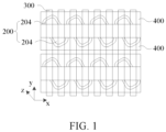
- FIG. 1 is a schematic structural diagram of a bit line, a word line, and an active pillar of a semiconductor structure in a related art. As shown in FIG. 1 , active pillars 200 in the related art are arranged in a hexagonal close-packed form. In this way, capacitor arrangement density in the DRAM device can be improved.
- An extension direction of a word line 400 and an extension direction of a bit line 300 are intersected with each other, and an included angle between the word line 400 and the bit line 300 may be a right angle.
- word lines 400 may extend in a direction x in FIG. 1 , and are arranged at intervals in a direction y; and bit lines 300 extend in the direction y, and are arranged at intervals in the direction x.
- An extension direction of the active pillar 200 is a direction z, and there is an included angle of less than 90 degrees between the direction z and the direction y. In the arrangement manner in FIG.
- one active pillar 200 has two storage node contacts 204 (SNC), and the two storage node contacts 204 are disconnected from each other and have a cut (AA Cut). Each storage node contact is correspondingly connected to one capacitor.
- SNC storage node contacts 204
- AA Cut cut
- Each storage node contact is correspondingly connected to one capacitor.
- two adjacent bit lines 300 are respectively connected to two storage node contacts 204 formed by breaking off one active pillar 200.
- a trench isolation structure is disposed in a substrate, an active pillar is defined by a first trench isolation structure and a second trench isolation structure of the trench isolation structure, a first end of the active pillar is exposed by a first surface of the substrate, a second end of the active pillar is opposite to the first end, and the second end is connected to a bit line.
- the bit line is defined by the first trench isolation structure, a plane extension direction of the bit line is the same as a plane extension direction of the first trench isolation structure, and the bit line is exposed by a second surface.
- both the bit line and the active pillar may be defined by the first trench isolation structure, to reduce difficulty in alignment between the active pillar and the bit line, and improve precision of alignment between the active pillar and the bit line.
- the foregoing structure helps reduce parasitic capacitance of the bit line and manufacturing difficulty, reduce contact resistance at a joint of the bit line and the active pillar, and improve stability of signal transmission on the bit line, thereby helping improve storage performance of a memory having the semiconductor structure.
- FIG. 2 is a schematic flowchart of a method for manufacturing a semiconductor structure according to an embodiment of the disclosure. As shown in FIG. 2 , for example, the manufacturing method includes the steps as follows.
- a substrate is provided.
- the substrate has a first initial surface and a second initial surface that are opposite to each other.
- FIG. 3 is a schematic structural diagram of forming a first isolation layer 1021 in a substrate 100 of a semiconductor structure according to an embodiment of the disclosure.
- the substrate 100 may be made of monocrystalline silicon, polysilicon, amorphous silicon, a silicon-germanium compound, silicon on insulator (SOI), or another material known to a person skilled in the art.
- the substrate 100 may be a structural basis supporting a trench isolation structure 101, a bit line 300, and a word line 400 that are disposed subsequently.
- the substrate 100 may be formed through deposition, e.g., chemical vapor deposition (CVD), physical vapor deposition (PVD), or atomic layer deposition (ALD).
- CVD chemical vapor deposition
- PVD physical vapor deposition
- ALD atomic layer deposition
- the substrate 100 may include a first initial surface 100a and a second initial surface 100b that are opposite to each other.
- the top surface of the substrate 100 is the first initial surface 100a
- the bottom surface is the second initial surface 100b.
- the substrate is processed from the first initial surface, to form an active pillar, a first trench and a second trench that define the active pillar, and an initial trench isolation structure filling the first trench and the second trench in the substrate.
- a plane extension direction of the first trench and a plane extension direction of the second trench are intersected with each other, the depth of the second trench is less than the depth of the first trench, and the first initial surface serves as a first surface of the substrate.
- a method for forming the first trench 102 and the second trench 103 in the substrate 100 may include the implementations as follows.
- that the substrate 100 is processed from the first initial surface 100a includes the step as follows.
- the substrate 100 is patterned from the first initial surface 100a, to form the first trench 102 and an active strip 203 defined by the first trench 102.
- the first trench 102 may extend in a first direction.
- the first isolation layer 1021 is filled in the first trench 102.
- a material of the first isolation layer 1021 may be silicon oxide, silicon nitride, silicon oxynitride, or the like.
- the first isolation layer 1021 fills the first trench 102, and is located between adjacent active strips 203, to effectively isolate the active strips 203.
- FIG. 4 is a schematic structural diagram of forming a first isolation layer and a second isolation layer in a substrate of a semiconductor structure according to an embodiment of the disclosure.
- FIG. 5 is a schematic structural diagram of forming an active pillar in a substrate of a semiconductor structure according to an embodiment of the disclosure.
- the second trench 103 extends in a second direction, and the first direction and the second direction are intersected with each other.
- the depth of the first trench 102 may be a as shown in FIG.
- the depth of the second trench 103 may be b as shown in FIG. 5 , and a is greater than b.
- the first trench 102 and the second trench 103 define the active pillar 200, and active pillars 200 are arranged in an array.
- the depth a of the first trench 102 may range from 150 nm to 200 nm, and the depth of the second trench 103 may range from 100 nm to 150 nm.
- a second isolation layer 1031 is filled in the second trench 103.
- the first trench 102 and the second trench 103 are communicated with each other, and the initial trench isolation structure includes the first isolation layer 1021 retained in the first trench 102 and the second isolation layer 1031 located in the second trench 103.
- a material of the second isolation layer 1031 may be silicon oxide, silicon nitride, silicon oxynitride, or the like, and the second isolation layer 1031 may isolate adjacent active pillars 200.
- the first isolation layer 1021 is filled in the first trench 102, to form a first trench isolation structure.
- the second isolation layer 1031 is filled in the second trench 103, to form a second trench isolation structure.
- the first trench isolation structure and the second trench isolation structure may jointly form the trench isolation structure 101.
- the material of the first isolation layer 1021 and the material of the second isolation layer 1031 are the same. In this way, manufacturing difficulty of the trench isolation structure 101 can be effectively reduced.
- the material of the first isolation layer 1021 and the material of the second isolation layer 1031 may alternatively be set to be different according to a requirement.
- that the substrate 100 is processed from the first initial surface 100a includes the step as follows.
- a mask layer is formed on the first initial surface 100a of the substrate 100.
- the mask layer has a first opening and a second opening that are communicated with each other, an extension direction of the first opening and an extension direction of the second opening are intersected with each other, and the width of the first opening is greater than the width of the second opening.
- first opening may extend in the first direction
- second opening may extend in the second direction.
- the substrate 100 is etched along the first opening and the second opening, to form the first trench 102 corresponding to the first opening and the second trench 103 corresponding to the second opening.
- the width of the first opening is greater than the width of the second opening. In an etching process, because of an etching loading effect, the depth of the formed first trench 102 is relatively large, and the depth of the second trench 103 is relatively small.
- the isolation material is filled in the first trench 102 and the second trench 103, to form the initial trench isolation structure.
- the isolation material may be silicon oxide, silicon nitride, silicon oxynitride, or the like.
- the isolation material filled in the first trench 102 forms the first trench isolation structure
- the isolation material filled in the second trench 103 forms the second trench isolation structure.
- the isolation material filled in the first trench 102 and the isolation material filled in the second trench 103 may alternatively be set to be different according to a requirement.
- the method for manufacturing a semiconductor structure further includes the step as follows.
- a vertical channel transistor is formed based on the active pillar 200.
- the active pillar 200 extends in a direction perpendicular to the substrate 100, and a transistor formed based on the active pillar 200 is a vertical channel transistor.
- the vertical channel transistor is formed based on the active pillar 200.
- the initial trench isolation structure is etched from the first surface 100c, to form a fourth trench.
- a depth of the fourth trench is less than the depth of the second trench 103, and a plane extension direction of the fourth trench is intersected with the first direction.
- the word line 400 is formed in the fourth trench.
- the word line 400 covers a partial sidewall of the active pillar 200.
- An isolation material is filled in the fourth trench in which the word line 400 is formed, to form a filling layer.
- the vertical channel transistor includes the active pillar 200 and the word line 400.
- the plane extension direction of the fourth trench is the same as the plane extension direction of the second trench 103.
- the initial trench isolation structure is etched from the first surface 100c, to form the fourth trench.
- the fourth trench may be located on one side of the active pillar 200, and the active pillar 200 is not exposed by the fourth trench; or the fourth trench may be located on one side of the active pillar 200, and the active pillar 200 may be exposed by the fourth trench in a partial plane direction; or the active pillar 200 is located in the fourth trench, and the active pillar 200 may be exposed by the fourth trench in any plane direction.
- the word line 400 is formed in the fourth trench, and in an extension direction of the active pillar 200, a channel region 200c is formed at a middle position in the extension direction of the active pillar 200, and a source region and a drain region are respectively formed at two ends of the extension direction of the active pillar 200. Therefore, the fourth trench corresponds to the middle position in the extension direction of the active pillar 200, and the depth of the fourth trench is less than the depth of the second trench 103.
- the extension direction of the fourth trench is an extension direction of the subsequently formed word line 400. To ensure that the plane extension direction of the word line 400 and a plane extension direction of the bit line 300 are intersected with each other, the plane extension direction of the fourth trench and the plane extension direction of the bit line 300 are intersected with each other.
- FIG. 6 is a schematic structural diagram of an active pillar of a semiconductor structure according to an embodiment of the disclosure.
- FIG. 6 shows a structure of a single active pillar 200.
- the word line 400 may cover at least a partial sidewall of the active pillar 200, to form the vertical channel transistor.
- a material of the word line 400 may be tungsten, and the word line 400 is formed in the fourth trench through deposition. It should be explained that active pillars 200 are on two sides of the second trench 103. Therefore, two fourth trenches corresponding to the active pillars 200 on the two sides may be formed in the second trench 103, and two word lines 400 are respectively formed in the two fourth trenches, and respectively correspond to the two active pillars 200.
- An isolation material is filled in the fourth trench in which the word line 400 is formed.
- the isolation material may be silicon oxide, silicon nitride, silicon oxynitride, or the like.
- the isolation material may be filled in the fourth trench through deposition. The isolation material may ensure structural stability of the word line 400 and stability of signal transmission in the word line 400.
- a manner in which the word line 400 covers the active pillar 200 may include the following implementations.
- one word line 400 may cover only one side of the channel region 200c of the active pillar 200, to form a single-sided gate structure of the vertical channel transistor.
- one word line 400 may cover two sides of the channel region 200c of the active pillar 200, to form a dual-sided gate structure of the vertical channel transistor.
- one word line 400 may surround a periphery of the channel region 200c of the active pillar 200, to form a gate-partially-around structure or a gate-all-around structure of the vertical channel transistor.
- a trench wall of the fourth trench may be of an initial trench isolation structure of a specific thickness, and the word line 400 and the channel region 200c of the active pillar 200 may be isolated by the initial trench isolation structure on the trench wall of the fourth trench, to form a gate dielectric layer of the vertical channel transistor (that is, the gate dielectric layer does not need to be specifically formed).
- the gate dielectric layer needs to be specifically formed when the word line 400 is formed.
- the initial trench isolation structure located in the second trench 103 is etched from the first surface 100c, to form a fifth trench.
- the depth of the fifth trench is less than the depth of the second trench 103, and a plane extension direction of the fifth trench is the same as the plane extension direction of the second trench 103.
- the word line 400 is formed in the fifth trench.
- the word line 400 covers a partial sidewall of the active pillar 200, and each active pillar 200 corresponds to two word lines 400.
- An isolation material is filled in the fifth trench in which the word line 400 is formed, to form a filling layer.
- the active pillar 200 and the initial trench isolation structure are etched from the first surface 100c, to form a sixth trench.
- the depth of the sixth trench is less than the depth of the second trench 103, a plane extension direction of the sixth trench being the same as the plane extension direction of the second trench 103, and the sixth trench divides the active pillar 200 into two active sub-pillars 201 and a connecting portion 202 connecting the two active sub-pillars 201.
- a dielectric layer is filled in the sixth trench, and an air gap 104 is formed.
- the vertical channel transistor includes one active sub-pillar 201 and one word line 400.
- the initial trench isolation structure is etched from the first surface 100c, to form the fifth trench.
- the second trench isolation structure in the second trench 103 may be etched, to form the fifth trench in the second trench 103.
- the word line 400 is formed in the fifth trench. Therefore, the fifth trench corresponds to the channel region 200c of the active pillar 200, and the depth of the fifth trench is less than the depth of the second trench 103.
- the plane extension direction of the word line 400 may be a plane extension direction of a fifth trench. Therefore, the plane extension direction of the fifth trench and the plane extension direction of the bit line 300 are intersected with each other.
- a specific material and a function of the isolation material filled in the fifth trench are the same as those of the isolation material filled in the fourth trench. Details are not described herein again.
- the active pillar 200 and the initial trench isolation structure are etched from the first surface 100c.
- the first trench isolation structure is etched, to form the sixth trench, and the sixth trench divides the active pillar 200 into the two active sub-pillars 201.
- the depth of the sixth trench is less than the depth of the second trench 103. In this way, the sixth trench may be prevented from cutting off the active pillar 200 in the extension direction of the active pillar 200 through etching, to ensure that the active pillar 200 with a partial extended length is retained at end portions of the two active sub-pillars 201, so as to form a connecting portion 202 connecting the two active sub-pillars 201.
- the dielectric layer is filled in the sixth trench through deposition.
- a material of the dielectric layer may be silicon oxide, silicon nitride, or silicon oxynitride.
- the material of the dielectric layer may be the same as the material of the isolation material, the material of the first isolation layer 1021, and the material of the second isolation layer 1031. In this way, manufacturing difficulty of the semiconductor structure can be reduced.
- a deposition process parameter of the dielectric layer may be controlled, to form the air gap 104 in the sixth trench.
- the air gap 104 may improve an effect of isolation between the two active sub-pillars 201, to avoid or reduce electrical interference between the active sub-pillars 201.
- FIG. 7 is a schematic structural diagram of another active pillar of a semiconductor structure according to an embodiment of the disclosure.
- FIG. 8 is a cross-sectional view of forming an active pillar in a substrate of a semiconductor structure according to an embodiment of the disclosure.
- the cross-sectional view shown in FIG. 8 is a cross-sectional view in the extension direction of the first trench 102 in FIG. 7 .
- a subsequent cross-sectional view is a cross-sectional view in the extension direction of the first trench 102.
- FIG. 7 and FIG. 8 show structures of the active pillar 200 with the air gap 104 and the word line 400.
- Two word lines 400 respectively cover at least partial sidewalls of the two active sub-pillars 201, to form two vertical channel transistors.
- one active sub-pillar 201 and one word line 400 form a vertical trench transistor.
- the subsequently formed bit line 300 is connected to the connecting portion 202, and the two active sub-pillars 201 are respectively connected to subsequently formed different storage structures 600.
- the bit line 300 inputs signals to the two active sub-pillars 201 through the connecting portion 202, and the word lines 400 corresponding to the two active sub-pillars 201 respectively control conduction and cutoff of the two active sub-pillars 201, to control the two active sub-pillars 201 to separately store signals in different storage structures 600 or read signals from different storage structures 600. In this way, a signal storage capability and signal transmission efficiency of the semiconductor structure can be effectively improved.
- the vertical channel transistor is formed based on the active pillar 200, and the active pillar 200 includes the source region, the drain region, and the channel region 200c.
- the word line 400 covers the outside of the channel region 200c of the active pillar 200.
- the source region and the drain region are respectively formed on two sides of the channel region 200c of the active pillar 200, and a formation process may include the step as follows. After the initial trench isolation structure is formed, an end portion that is of the active pillar 200 and that is exposed by the first surface 100c is doped from the first surface 100c, to form a first doped region 200a.
- the end portion that is of the active pillar 200 and that is exposed by the first surface 100c may be a first end of the active pillar 200, and the first doped region 200a formed at the first end may be one of the source region and the drain region of the active pillar 200.
- an end portion that is of the active pillar 200 and that is close to the second surface 100d is doped from the second surface 100d, to form a second doped region 200b.
- the end portion that is of the active pillar 200 and that is close to the second surface 100d may be a second end opposite to the first end, and the second doped region 200b formed at the second end may be the other one of the source region and the drain region of the active pillar 200.
- the method for manufacturing a semiconductor structure further includes the step as follows.
- the storage structure 600 is formed.
- the storage structure 600 is located on the first surface 100c of the substrate 100, and the storage structure 600 is coupled to the vertical channel transistor.
- FIG. 9 is a cross-sectional view of forming a storage structure and an auxiliary substrate on a substrate of a semiconductor structure according to an embodiment of the disclosure. As shown in FIG. 9 , the storage structure 600 may be located on the first surface 100c of the substrate 100. In other words, in a direction shown in FIG. 9 , the storage structure 600 is located on the top of the substrate 100 with the vertical channel transistor.
- the storage structure 600 may be a capacitor, or may be a magnetic tunnel junction (MTJ).
- a specific type of the storage structure 600 is not limited in the disclosure.
- An example in which the storage structure 600 is a capacitor is utilized for description in this embodiment of the disclosure.
- the capacitor may include multiple capacitors 601.
- the multiple capacitors 601 are arranged in an array.
- a capacitor isolation layer 602 made of an insulating material is disposed between adjacent capacitors 601. The capacitor isolation layer 602 may prevent electrical interference between the adjacent capacitors 601.
- the first end of the active pillar 200 may be coupled to the capacitor.
- one active sub-pillar 201 of the active pillar 200 is correspondingly connected to one capacitor, and a vertical channel transistor formed based on the active sub-pillar 201 may control signal input or signal reading of the corresponding connected capacitor.
- an auxiliary substrate 100e may be formed on the top of the storage structure 600, and the auxiliary substrate 100e may have a support effect.
- the auxiliary substrate 100e may support the substrate 100 and the vertical channel transistor in the substrate 100.
- a material of the auxiliary substrate 100e may be the same as a material of the substrate 100, to reduce complexity of a manufacturing process of the semiconductor structure.
- the thickness of the auxiliary substrate 100e may be set according to a requirement. This is not limited in the disclosure.
- the bit line 300 is formed.
- a specific method for forming the bit line 300 includes the step as follows. In the step of S300, the substrate is thinned from the second initial surface, until the initial trench isolation structure in the first trench is exposed. A surface, opposite to the first surface, of the thinned substrate serves as the second surface of the substrate.
- FIG. 10 is a schematic structural diagram of a semiconductor structure with a substrate flipped over according to an embodiment of the disclosure.
- FIG. 11 is a cross-sectional view of a semiconductor structure with a substrate flipped over according to an embodiment of the disclosure.
- the substrate 100 may be flipped over, so that the second initial surface 100b of the substrate 100 is located on the top surface of the substrate 100. In this way, difficulty in processing the second initial surface 100b can be reduced. That is, directions of structures shown in FIG. 10 and FIG. 11 are directions obtained after a structure shown in FIG. 9 is turned upside down.
- FIG. 12 is a schematic structural diagram of a semiconductor structure with a substrate thinned according to an embodiment of the disclosure.
- FIG. 13 is a cross-sectional view of a semiconductor structure with a substrate thinned according to an embodiment of the disclosure. As shown in FIG. 12 and FIG. 13 , the second initial surface 100b is thinned. Such processing may be completed with a chemical mechanical polishing (CMP) process.
- CMP chemical mechanical polishing
- the first trench 102 is exposed before the second trench 103 in a process of thinning the second surface 100d of the substrate 100, and correspondingly, the first isolation layer 1021 in the first trench 102 is also exposed.
- the top surface of the thinned substrate 100 namely, a surface opposite to the first surface 100c forms the second surface 100d of the substrate 100.
- the substrate is etched from the second surface, to form a third trench.
- a plane extension direction of the third trench is the same as the plane extension direction of the first trench.
- FIG. 14 is a schematic structural diagram of forming a third trench in a semiconductor structure according to an embodiment of the disclosure.
- FIG. 15 is a cross-sectional view of forming a third trench in a semiconductor structure according to an embodiment of the disclosure.
- the substrate 100 of a partial thickness between adjacent first trenches 102 is removed, to form the third trench 105.
- the first trench 102 and the second trench 103 define the active pillar 200. Therefore, both the first trench 102 and the second trench 103 expose a part of the active pillar 200. Based on this, the depth of the third trench 105 may be relatively large, to ensure that the third trench 105 may expose the second trench 103 and the second isolation layer 1031 in the second trench 103.
- the depth of the third trench 105 may alternatively be relatively small, to ensure that the third trench 105 exposes only the first trench 102 and the first isolation layer 1021 in the first trench 102. Both the foregoing two depths of the third trench 105 can ensure that the third trench 105 exposes the active pillar 200.
- the plane extension direction of the third trench 105 is parallel to the plane extension direction of the first trench 102, and the third trench 105 is located between the adjacent first trenches 102.
- bit line 300 is formed in the third trench 105.
- the step as follows is further included.
- a bit line contact structure 500 is formed.
- the bit line contact structure 500 is configured to connect the second doped region 200b of the active pillar 200 and the bit line 300.
- FIG. 16 is a schematic structural diagram of forming a contact material in a semiconductor structure according to an embodiment of the disclosure.
- FIG. 17 is a cross-sectional view of forming a contact material in a semiconductor structure according to an embodiment of the disclosure.
- that the bit line contact structure 500 is formed includes the step as follows.
- a contact material 501 is deposited in the third trench 105.
- the contact material 501 may be cobalt.
- the contact material 501 and the substrate 100 react through heat treatment.
- the substrate 100 is silicon
- the contact material 501 is cobalt. Cobalt and silicon react through heat treatment, to generate a cobalt-silicon compound.
- FIG. 18 is a schematic structural diagram of forming a bit line contact structure in a semiconductor structure according to an embodiment of the disclosure.
- FIG. 19 is a cross-sectional view of forming a bit line contact structure in a semiconductor structure according to an embodiment of the disclosure. As shown in FIG. 18 and FIG. 19 , the cobalt-silicon compound forms the bit line contact structure 500.
- bit line contact structure 500 After the bit line contact structure 500 is formed, the step as follows is further included.
- the bit line is formed in the third trench.
- the bit line is connected to the end portion that is of the active pillar and that is close to the second surface, and the bit line is defined by the initial trench isolation structure located in the first trench.
- FIG. 20 is a schematic structural diagram of forming a bit line material in a semiconductor structure according to an embodiment of the disclosure.
- FIG. 21 is a schematic structural diagram of forming a bit line in a semiconductor structure according to an embodiment of the disclosure.
- FIG. 22 is a cross-sectional view of forming a bit line in a semiconductor structure according to an embodiment of the disclosure.
- the bit line 300 may be formed through deposition.
- a bit line material 301 is deposited, and the bit line material 301 may be at least one of titanium nitride and tungsten.
- the bit line material 301 may completely cover the second surface 100d of the substrate 100, and is filled in the third trench 105.
- a structure of the bit line material 301 refer to FIG. 20 .
- a bit line material 301 outside the third trench 105 is removed with the CMP process or an etching back process, the bit line material 301 located in the third trench 105 is retained, and the bit line 300 is formed.
- the bit line material 301 includes titanium nitride and tungsten.
- the formed bit line 300 includes a titanium nitride layer and a tungsten layer.
- the third trench 105 is located between adjacent first trenches 102. Therefore, the bit line 300 is formed in the third trench 105, and the bit line 300 may be defined by the first trench 102. In this way, it can be ensured that the bit line 300 and the active pillar 200 are precisely aligned, to reduce difficulty in alignment between the bit line 300 and the active pillar 200, and improve precision of alignment between the bit line 300 and the active pillar 200, thereby helping improve an effect of signal transmission between the bit line 300 and the active pillar 200.
- the disclosure provides a semiconductor structure.
- the semiconductor structure may be manufactured through the foregoing method for manufacturing a semiconductor structure.
- the semiconductor structure includes a substrate 100, an active pillar 200, a bit line 300, and a trench isolation structure 101.
- the substrate 100 has a first surface 100c and a second surface 100d that are opposite to each other.
- the trench isolation structure 101 is located in the substrate 100, the trench isolation structure 101 includes a first trench isolation structure and a second trench isolation structure that extend from the first surface 100c to the second surface 100d, the first trench isolation structure is exposed by the first surface 100c and the second surface 100d, and the second trench isolation structure is exposed by the first surface 100c.
- the active pillar 200 is defined by the first trench isolation structure and the second trench isolation structure, a first end of the active pillar 200 is exposed by the first surface 100c, a second end of the active pillar 200 is opposite to the first end, and the second end is connected to the bit line 300.
- the bit line 300 is defined by the first trench isolation structure, a plane extension direction of the bit line 300 is the same as a plane extension direction of the first trench isolation structure, and the bit line 300 is exposed by the second surface 100d.
- the active pillar 200, the bit line 300, and a word line 400 in the disclosure may be located in the substrate 100, and the substrate 100 may provide a structural basis for the active pillar 200, the bit line 300, and the word line 400.
- the active pillar 200 may be defined by the first trench isolation structure and the second trench isolation structure, and the first trench isolation structure and the second trench isolation structure can effectively isolate adjacent active pillars 200, to ensure stability of electrical signal transmission in the active pillar 200.
- the first trench isolation structure and the second trench isolation structure may support the active pillar 200 from sidewalls of the active pillar 200, to prevent the active pillar 200 from being tilted or collapsed during manufacturing and utilization, thereby improving structural stability of the active pillar 200.
- the first trench isolation structure is exposed by the first surface 100c and the second surface 100d of the substrate 100 that are opposite to each other, and the second trench isolation structure is exposed by the first surface 100c.
- the first end of the active pillar 200 is exposed on the first surface 100c. Therefore, the first end of the active pillar 200 is defined by the first trench isolation structure and the second trench isolation structure.
- the second end of the active pillar 200 extends to the second surface 100d, and the bit line 300 is located on the second surface 100d of the substrate 100, and is defined by the first trench isolation structure.
- the bit line 300 is connected to the second end of the active pillar 200.
- the second end of the active pillar 200 and the bit line 300 are jointly defined by the first trench isolation structure, difficulty in alignment between the bit line 300 and the active pillar 200 is effectively reduced, and precision of alignment between the bit line 300 and the active pillar 200 is improved, to ensure electrical signal transmission between the bit line 300 and the active pillar 200.
- the semiconductor structure further includes a storage structure 600.
- the storage structure 600 is located on the first surface 100c of the substrate 100, and the storage structure 600 is coupled to a vertical channel transistor.
- the semiconductor structure provided in the disclosure forms a memory array 700, and multiple memory arrays 700 jointly form a memory.
- FIG. 23 is a schematic structural diagram of a memory array formed based on a semiconductor structure according to an embodiment of the disclosure.
- FIG. 24 is a partially enlarged view of a portion B in FIG. 23.
- FIG. 25 is a schematic structural diagram of a bit line and an active pillar of a semiconductor structure according to an embodiment of the disclosure.
- a substrate 100 of each memory array 700 in this embodiment of the disclosure includes multiple active pillars 200 and multiple storage structures 600.
- the multiple active pillars 200 are arranged in an array in the substrate 100, the multiple storage structures 600 are arranged in an array on the substrate 100, and the multiple storage structures 600 and the multiple active pillars 200 are coupled in one-to-one correspondence.
- the memory array 700 further includes multiple word lines 400 and multiple bit lines 300, plane extension directions of the multiple word lines 400 are parallel to each other, plane extension directions of the multiple bit lines 300 are parallel to each other, and the plane extension direction of the word line 400 and the plane extension direction of the bit line 300 are intersected with each other.
- One bit line 300 is connected to second ends of the multiple active pillars 200, and one word line 400 corresponds to channel regions 200c of active sub-pillars 201 of the multiple active pillars 200.
- the multiple memory arrays 700 may jointly form the memory, and the multiple memory arrays 700 are arranged in an array.
- a sub-word line driver 701 is disposed between two adjacent memory arrays 700, and the sub-word line driver circuit 701 is connected to word lines 400 of the corresponding adjacent memory arrays 700, and is configured to drive the word line 400.
- a sense amplifier 702 is disposed between two adjacent memory arrays 700, and the sense amplifier 702 is connected to bit lines 300 of the corresponding adjacent memory arrays 700, and is configured to process an electrical signal on the bit line 300.
- the active pillars 200 are arranged in a hexagonal close-packed form, and the storage structures 600 may have the same arrangement manner as the active pillars 200, to not only reduce difficulty in connecting the storage structure 600 and the active pillar 200, but also reduce manufacturing difficulty of the semiconductor structure.
- a hexagonal close-packed arrangement manner can effectively improve arrangement density of the storage structure 600, thereby improving a storage amount of the semiconductor structure and helping improve storage performance of the semiconductor structure.
- FIG. 24 shows the active pillar 200, or may show a storage node contact structure of the active pillar 200.
- the plane extension direction of the bit line 300 is a direction z shown in FIG. 24
- the plane extension direction of the word line 400 is a direction x shown in FIG. 24
- an included angle between the bit line 300 and the word line 400 ranges from 20° to 90°.
- the included angle between the bit line 300 and the word line 400 may be 30°, 60°, or 75°.
- a specific value of the included angle is not limited in the disclosure.
- the included angle between the bit line 300 and the word line 400 may be 60°, so that the storage structure 600 is set to be in a hexagonal close-packed form.
- both the second end of the active pillar 200 and the bit line 300 are defined by the first trench isolation structure, and a plane extension direction of the second end of the active pillar 200 and the plane extension direction of the bit line 300 are the same.
- An orthographic projection of the second end of the active pillar 200 in a plane in which the bit line 300 is located may be covered by the bit line 300. In this way, precision of alignment between the active pillar 200 and the bit line 300 can be effectively improved, and an effect of alignment between the active pillar 200 and the bit line 300 is ensured.
- the disclosure has the advantages as follows.
- the disclosure can reduce a quantity of bit lines 300 while ensuring stable signal transmission of the active pillar 200. In this way, manufacturing difficulty of the bit line 300 can be reduced, and adjacent bit lines 300 are prevented from being short-circuited.
- the width of a single bit line 300 is prevented from being too small, to help reduce parasitic capacitance of the bit line 300, avoid excessive contact resistance between the bit line 300 and the active pillar 200, and improve an effect of electric signal transmission between the bit line 300 and the active pillar 200, thereby ensuring storage performance of a memory including the semiconductor structure.
- the active pillar 200 includes a first doped region 200a exposed by the first surface 100c, a second doped region 200b close to the second surface 100d, and a channel region 200c located between the first doped region 200a and the second doped region 200b.
- the semiconductor structure further includes the word line 400.
- the word line 400 is located in the trench isolation structure 101, and covers the channel region 200c of the active pillar 200.
- the active pillar 200 and the word line 400 form the vertical channel transistor.
- the first doped region 200a may be one of a source region and a drain region of the vertical channel transistor, and the second doped region 200b may be the other one.
- the word line 400 covers the channel region 200c, and a gate dielectric layer may exist between the word line 400 and the channel region 200c, to ensure a gate control capability of the vertical channel transistor.
- the plane extension direction of the word line 400 is the same as a plane extension direction of the second trench isolation structure.
- adjacent word lines 400 may be isolated by the second trench isolation structure, to avoid electrical interference between the adjacent word lines 400.
- the second trench isolation structure may support the word line 400, to avoid damage to a structure of the word line 400, and improve structural stability of the word line 400.
- the active pillar 200 and the word line 400 may jointly form the vertical channel transistor, and a position relationship between the word line 400 and the active pillar 200 is adjusted, so that the vertical channel transistor forms a single-sided gate structure, a dual-sided gate structure, or a gate-all-around structure. A specific position relationship is described in detail in the foregoing embodiment of the method for manufacturing a semiconductor structure. Details are not described herein again.
- the active pillar 200 includes two active sub-pillars 201 and a connecting portion 202 connecting the two active sub-pillars 201, an air gap 104 is formed between the two active sub-pillars 201, and each active sub-pillar 201 includes a first doped region 200a exposed by the first surface 100c, a second doped region 200b close to the second surface 100d, and a channel region 200c located between the first doped region 200a and the second doped region 200b.
- the semiconductor structure further includes the word line 400.
- the word line 400 is located in the trench isolation structure 101, and covers the channel region 200c of the active sub-pillar 201.
- Each active sub-pillar 201 and one word line 400 form the vertical channel transistor.
- the connecting portion 202 may be close to the second surface 100d of the substrate 100, form the second end of the active pillar 200, and is doped to form the second doped region 200b.
- the second doped region 200b may be one of a source region and a drain region of the active pillar 200, and the second doped region 200b is connected to the bit line 300.
- First ends that are of the two active sub-pillars 201 and that are close to the first surface 100c are doped to form first doped regions 200a, and the first doped region 200a may be the other one in the source region and the drain region of the active pillar 200.
- the first doped regions 200a of the two active sub-pillars 201 are separately connected to different storage structures 600.
- one active pillar 200 includes two active sub-pillars 201, and one active sub-pillar 201 corresponds to one word line 400 to form the vertical channel transistor.
- a quantity of vertical channel transistors in the semiconductor structure may be effectively improved, and storage performance of the memory including the semiconductor structure is improved.
- the semiconductor structure in the disclosure further includes a bit line contact structure 500, and the bit line contact structure 500 is located between the active pillar 200 and the bit line 300, and connects the second end of the active pillar 200 and the bit line 300.
- the bit line contact structure 500 can effectively reduce contact resistance between the bit line 300 and the active pillar 200.
- multiple bit line contact structures 500 connected to the same bit line 300 are discrete or integrated. Integrally disposed multiple bit line contact structures 500 may be simultaneously connected to multiple active pillars 200 corresponding to the same bit line 300, to effectively reduce manufacturing difficulty of the bit line contact structure 500, and ensure stability of connecting the multiple active pillars 200 and the same bit line 300. Separately disposed bit line contact structures 500 may be located in different third trenches 105 defined by the first trench isolation structure. When a bit line contact structure 500 at a joint of a specific active pillar 200 and the bit line 300 is adjusted, a connection between the retained active pillars 200 and the bit line 300 is not affected, so that structural flexibility of the bit line contact structure 500 can be improved.
- the disclosure provides a memory.
- the memory may include the foregoing semiconductor structure.
- the memory may include a DRAM, a static random access memory (SRAM), a flash memory, an electrically erasable programmable read-only memory (EEPROM), a phase change random access memory (PRAM), or a magneto-resistive random access memory (MRAM).
- DRAM dynamic random access memory
- SRAM static random access memory
- EEPROM electrically erasable programmable read-only memory
- PRAM phase change random access memory
- MRAM magneto-resistive random access memory
Landscapes
- Engineering & Computer Science (AREA)
- Manufacturing & Machinery (AREA)
- Semiconductor Memories (AREA)
- Element Separation (AREA)
Applications Claiming Priority (2)
| Application Number | Priority Date | Filing Date | Title |
|---|---|---|---|
| CN202310070761.3A CN118382288A (zh) | 2023-01-13 | 2023-01-13 | 半导体结构及其制备方法 |
| PCT/CN2023/092777 WO2024148722A1 (zh) | 2023-01-13 | 2023-05-08 | 半导体结构及其制备方法 |
Publications (2)
| Publication Number | Publication Date |
|---|---|
| EP4465786A1 true EP4465786A1 (de) | 2024-11-20 |
| EP4465786A4 EP4465786A4 (de) | 2025-06-25 |
Family
ID=91897847
Family Applications (1)
| Application Number | Title | Priority Date | Filing Date |
|---|---|---|---|
| EP23915486.7A Pending EP4465786A4 (de) | 2023-01-13 | 2023-05-08 | Halbleiterstruktur und herstellungsverfahren dafür |
Country Status (4)
| Country | Link |
|---|---|
| US (1) | US20240422962A1 (de) |
| EP (1) | EP4465786A4 (de) |
| CN (1) | CN118382288A (de) |
| WO (1) | WO2024148722A1 (de) |
Family Cites Families (11)
| Publication number | Priority date | Publication date | Assignee | Title |
|---|---|---|---|---|
| DE19843979C1 (de) * | 1998-09-24 | 2000-03-02 | Siemens Ag | Speicherzellenanordnung mit ferroelektrischem oder dynamischen Speicherzellen und entsprechendes Herstellungsverfahren |
| US7746680B2 (en) * | 2007-12-27 | 2010-06-29 | Sandisk 3D, Llc | Three dimensional hexagonal matrix memory array |
| US9245893B1 (en) * | 2014-11-19 | 2016-01-26 | Micron Technology, Inc. | Semiconductor constructions having grooves dividing active regions |
| CN115172370A (zh) * | 2021-04-07 | 2022-10-11 | 芯盟科技有限公司 | 半导体结构及其形成方法 |
| CN113611667B (zh) * | 2021-07-02 | 2024-09-10 | 芯盟科技有限公司 | 晶体管阵列及其制造方法、半导体器件及其制造方法 |
| CN113488468A (zh) * | 2021-07-07 | 2021-10-08 | 芯盟科技有限公司 | 半导体结构及半导体结构的形成方法 |
| CN114141715B (zh) * | 2021-11-30 | 2023-06-23 | 长鑫存储技术有限公司 | 半导体结构的制作方法及半导体结构 |
| CN114373720A (zh) * | 2022-01-19 | 2022-04-19 | 芯盟科技有限公司 | 动态随机存取存储器的形成方法 |
| CN114783954B (zh) * | 2022-04-08 | 2026-02-10 | 芯盟科技有限公司 | 半导体结构及其制造方法、存储器 |
| CN115117064A (zh) * | 2022-06-24 | 2022-09-27 | 长鑫存储技术有限公司 | 半导体结构及其形成方法 |
| CN115295496A (zh) * | 2022-08-26 | 2022-11-04 | 长江存储科技有限责任公司 | 半导体器件及其制备方法、存储器以及存储系统 |
-
2023
- 2023-01-13 CN CN202310070761.3A patent/CN118382288A/zh active Pending
- 2023-05-08 WO PCT/CN2023/092777 patent/WO2024148722A1/zh not_active Ceased
- 2023-05-08 EP EP23915486.7A patent/EP4465786A4/de active Pending
-
2024
- 2024-08-27 US US18/817,191 patent/US20240422962A1/en active Pending
Also Published As
| Publication number | Publication date |
|---|---|
| US20240422962A1 (en) | 2024-12-19 |
| WO2024148722A1 (zh) | 2024-07-18 |
| CN118382288A (zh) | 2024-07-23 |
| EP4465786A4 (de) | 2025-06-25 |
Similar Documents
| Publication | Publication Date | Title |
|---|---|---|
| US11488956B2 (en) | Semiconductor memory device | |
| US7569878B2 (en) | Fabricating a memory cell array | |
| US20070224753A1 (en) | Vertical wrap-around-gate field-effect-transistor for high density, low voltage logic and memory array | |
| US20020137271A1 (en) | Flash memory with ultra thin vertical body transistors | |
| WO2023272881A1 (zh) | 晶体管阵列及其制造方法、半导体器件及其制造方法 | |
| JP2011211153A (ja) | 半導体装置及びその製作方法 | |
| CN115295496A (zh) | 半导体器件及其制备方法、存储器以及存储系统 | |
| US6492221B1 (en) | DRAM cell arrangement | |
| CN113270413A (zh) | 半导体存储器件 | |
| KR102642487B1 (ko) | 반도체 장치 및 그 제조 방법 | |
| TW202418949A (zh) | 半導體元件 | |
| EP4465786A1 (de) | Halbleiterstruktur und herstellungsverfahren dafür | |
| WO2014126214A1 (ja) | 半導体装置 | |
| US12369313B2 (en) | Semiconductor structure and method for fabricating the same | |
| JP7652938B2 (ja) | メモリ及びその製造方法 | |
| US12046630B2 (en) | Manufacturing method of semiconductor structure and semiconductor structure | |
| CN116406164A (zh) | 半导体结构及其制备方法 | |
| CN115274668A (zh) | 存储器件及其制造方法及包括该存储器件的电子设备 | |
| WO2022077950A1 (zh) | 埋入式位线及其形成方法 | |
| CN119155988B (zh) | 存储单元、存储器及其制备方法 | |
| US20240274664A1 (en) | Integrated circuit devices | |
| US20250226316A1 (en) | Dram cell structure and method for manufacturing the same | |
| US20250081444A1 (en) | Semiconductor memory device and method for manufacturing the same | |
| US20250142805A1 (en) | Semiconductor memory device | |
| CN120021375A (zh) | 存储阵列及其制备方法、存储器、电子设备 |
Legal Events
| Date | Code | Title | Description |
|---|---|---|---|
| STAA | Information on the status of an ep patent application or granted ep patent |
Free format text: STATUS: THE INTERNATIONAL PUBLICATION HAS BEEN MADE |
|
| PUAI | Public reference made under article 153(3) epc to a published international application that has entered the european phase |
Free format text: ORIGINAL CODE: 0009012 |
|
| STAA | Information on the status of an ep patent application or granted ep patent |
Free format text: STATUS: REQUEST FOR EXAMINATION WAS MADE |
|
| 17P | Request for examination filed |
Effective date: 20240816 |
|
| AK | Designated contracting states |
Kind code of ref document: A1 Designated state(s): AL AT BE BG CH CY CZ DE DK EE ES FI FR GB GR HR HU IE IS IT LI LT LU LV MC ME MK MT NL NO PL PT RO RS SE SI SK SM TR |
|
| A4 | Supplementary search report drawn up and despatched |
Effective date: 20250527 |
|
| RIC1 | Information provided on ipc code assigned before grant |
Ipc: H10B 12/00 20230101AFI20250521BHEP |
|
| STAA | Information on the status of an ep patent application or granted ep patent |
Free format text: STATUS: EXAMINATION IS IN PROGRESS |
|
| 17Q | First examination report despatched |
Effective date: 20251202 |