EP4451324A1 - Semiconductor device, electronic device and method for producing semiconductor device - Google Patents
Semiconductor device, electronic device and method for producing semiconductor device Download PDFInfo
- Publication number
- EP4451324A1 EP4451324A1 EP22907054.5A EP22907054A EP4451324A1 EP 4451324 A1 EP4451324 A1 EP 4451324A1 EP 22907054 A EP22907054 A EP 22907054A EP 4451324 A1 EP4451324 A1 EP 4451324A1
- Authority
- EP
- European Patent Office
- Prior art keywords
- front surface
- transparent member
- glass
- sealing resin
- substrate
- Prior art date
- Legal status (The legal status is an assumption and is not a legal conclusion. Google has not performed a legal analysis and makes no representation as to the accuracy of the status listed.)
- Pending
Links
Images








Classifications
-
- H—ELECTRICITY
- H10—SEMICONDUCTOR DEVICES; ELECTRIC SOLID-STATE DEVICES NOT OTHERWISE PROVIDED FOR
- H10F—INORGANIC SEMICONDUCTOR DEVICES SENSITIVE TO INFRARED RADIATION, LIGHT, ELECTROMAGNETIC RADIATION OF SHORTER WAVELENGTH OR CORPUSCULAR RADIATION
- H10F39/00—Integrated devices, or assemblies of multiple devices, comprising at least one element covered by group H10F30/00, e.g. radiation detectors comprising photodiode arrays
- H10F39/10—Integrated devices
- H10F39/12—Image sensors
-
- H—ELECTRICITY
- H10—SEMICONDUCTOR DEVICES; ELECTRIC SOLID-STATE DEVICES NOT OTHERWISE PROVIDED FOR
- H10F—INORGANIC SEMICONDUCTOR DEVICES SENSITIVE TO INFRARED RADIATION, LIGHT, ELECTROMAGNETIC RADIATION OF SHORTER WAVELENGTH OR CORPUSCULAR RADIATION
- H10F39/00—Integrated devices, or assemblies of multiple devices, comprising at least one element covered by group H10F30/00, e.g. radiation detectors comprising photodiode arrays
- H10F39/80—Constructional details of image sensors
- H10F39/804—Containers or encapsulations
-
- H—ELECTRICITY
- H10—SEMICONDUCTOR DEVICES; ELECTRIC SOLID-STATE DEVICES NOT OTHERWISE PROVIDED FOR
- H10F—INORGANIC SEMICONDUCTOR DEVICES SENSITIVE TO INFRARED RADIATION, LIGHT, ELECTROMAGNETIC RADIATION OF SHORTER WAVELENGTH OR CORPUSCULAR RADIATION
- H10F39/00—Integrated devices, or assemblies of multiple devices, comprising at least one element covered by group H10F30/00, e.g. radiation detectors comprising photodiode arrays
- H10F39/011—Manufacture or treatment of image sensors covered by group H10F39/12
-
- H—ELECTRICITY
- H10—SEMICONDUCTOR DEVICES; ELECTRIC SOLID-STATE DEVICES NOT OTHERWISE PROVIDED FOR
- H10F—INORGANIC SEMICONDUCTOR DEVICES SENSITIVE TO INFRARED RADIATION, LIGHT, ELECTROMAGNETIC RADIATION OF SHORTER WAVELENGTH OR CORPUSCULAR RADIATION
- H10F39/00—Integrated devices, or assemblies of multiple devices, comprising at least one element covered by group H10F30/00, e.g. radiation detectors comprising photodiode arrays
- H10F39/80—Constructional details of image sensors
- H10F39/806—Optical elements or arrangements associated with the image sensors
-
- H—ELECTRICITY
- H10—SEMICONDUCTOR DEVICES; ELECTRIC SOLID-STATE DEVICES NOT OTHERWISE PROVIDED FOR
- H10W—GENERIC PACKAGES, INTERCONNECTIONS, CONNECTORS OR OTHER CONSTRUCTIONAL DETAILS OF DEVICES COVERED BY CLASS H10
- H10W74/00—Encapsulations, e.g. protective coatings
- H10W74/01—Manufacture or treatment
-
- H—ELECTRICITY
- H10—SEMICONDUCTOR DEVICES; ELECTRIC SOLID-STATE DEVICES NOT OTHERWISE PROVIDED FOR
- H10W—GENERIC PACKAGES, INTERCONNECTIONS, CONNECTORS OR OTHER CONSTRUCTIONAL DETAILS OF DEVICES COVERED BY CLASS H10
- H10W74/00—Encapsulations, e.g. protective coatings
- H10W74/10—Encapsulations, e.g. protective coatings characterised by their shape or disposition
- H10W74/131—Encapsulations, e.g. protective coatings characterised by their shape or disposition the semiconductor body being only partially enclosed
- H10W74/141—Encapsulations, e.g. protective coatings characterised by their shape or disposition the semiconductor body being only partially enclosed the encapsulations being on at least the sidewalls of the semiconductor body
-
- H—ELECTRICITY
- H10—SEMICONDUCTOR DEVICES; ELECTRIC SOLID-STATE DEVICES NOT OTHERWISE PROVIDED FOR
- H10W—GENERIC PACKAGES, INTERCONNECTIONS, CONNECTORS OR OTHER CONSTRUCTIONAL DETAILS OF DEVICES COVERED BY CLASS H10
- H10W76/00—Containers; Fillings or auxiliary members therefor; Seals
- H10W76/10—Containers or parts thereof
- H10W76/12—Containers or parts thereof characterised by their shape
-
- H—ELECTRICITY
- H10—SEMICONDUCTOR DEVICES; ELECTRIC SOLID-STATE DEVICES NOT OTHERWISE PROVIDED FOR
- H10F—INORGANIC SEMICONDUCTOR DEVICES SENSITIVE TO INFRARED RADIATION, LIGHT, ELECTROMAGNETIC RADIATION OF SHORTER WAVELENGTH OR CORPUSCULAR RADIATION
- H10F39/00—Integrated devices, or assemblies of multiple devices, comprising at least one element covered by group H10F30/00, e.g. radiation detectors comprising photodiode arrays
- H10F39/10—Integrated devices
- H10F39/12—Image sensors
- H10F39/18—Complementary metal-oxide-semiconductor [CMOS] image sensors; Photodiode array image sensors
-
- H—ELECTRICITY
- H10—SEMICONDUCTOR DEVICES; ELECTRIC SOLID-STATE DEVICES NOT OTHERWISE PROVIDED FOR
- H10F—INORGANIC SEMICONDUCTOR DEVICES SENSITIVE TO INFRARED RADIATION, LIGHT, ELECTROMAGNETIC RADIATION OF SHORTER WAVELENGTH OR CORPUSCULAR RADIATION
- H10F39/00—Integrated devices, or assemblies of multiple devices, comprising at least one element covered by group H10F30/00, e.g. radiation detectors comprising photodiode arrays
- H10F39/80—Constructional details of image sensors
-
- H—ELECTRICITY
- H10—SEMICONDUCTOR DEVICES; ELECTRIC SOLID-STATE DEVICES NOT OTHERWISE PROVIDED FOR
- H10F—INORGANIC SEMICONDUCTOR DEVICES SENSITIVE TO INFRARED RADIATION, LIGHT, ELECTROMAGNETIC RADIATION OF SHORTER WAVELENGTH OR CORPUSCULAR RADIATION
- H10F39/00—Integrated devices, or assemblies of multiple devices, comprising at least one element covered by group H10F30/00, e.g. radiation detectors comprising photodiode arrays
- H10F39/80—Constructional details of image sensors
- H10F39/811—Interconnections
Definitions
- the present disclosure relates to a semiconductor device, an electronic apparatus, and a manufacturing method of a semiconductor device.
- a semiconductor device including an imaging element such as a CMOS image sensor and a semiconductor element such as a light-emitting element such as a semiconductor laser there has been a device including the following package structure in the past. That is, a package structure in which a transparent member such as a plate-like glass is provided so as to cover a semiconductor element mounted on a substrate from an upper side (front surface side) and a sealing resin part is provided around the semiconductor element and the transparent member on the substrate has been provided (see, for example, PTL 1).
- a semiconductor chip In a manufacturing process of a semiconductor device, a semiconductor chip is generally picked up by a suction collet when the semiconductor chip is conveyed.
- the semiconductor chip In the case of the semiconductor chip having the package structure as described above, the semiconductor chip is subjected to suction by the collet on a side where the transparent member is provided to the semiconductor element.
- a front surface (upper surface) of the transparent member becomes the uppermost surface in the package structure. Therefore, when being picked up by the collet, the semiconductor chip is subjected to a suction action by the collet on the front surface of the transparent member.
- An object of the present technique is to provide a semiconductor device, an electronic apparatus, and a manufacturing method of a semiconductor device that can suppress the occurrence of scratches and stains on a transparent member provided so as to cover a semiconductor element from the front surface side and can stabilize the manufacturing yield.
- a semiconductor device includes a substrate, a semiconductor element that is provided on the substrate, a transparent member that is provided on the semiconductor element through a support part, and a sealing resin part that is formed around the semiconductor element and the transparent member on the substrate, and the sealing resin part has a protrusion part having an upper surface thereof perpendicular to a plate thickness direction of the substrate, the upper surface being positioned above a front surface of the transparent member in the plate thickness direction.
- a dimension between the front surface of the transparent member and the upper surface of the protrusion part is 10 to 200 ⁇ m in the plate thickness direction.
- the transparent member has a rectangular plate-like outer shape with one plate surface as the front surface
- the protrusion part is formed in a frame shape by four side parts along a rectangular outer shape of the transparent member in plan view, and a width of each side part of the protrusion part is 100 ⁇ m or more.
- the protrusion part has a transparent member covering part extending on the front surface of the transparent member so as to cover an edge part of the front surface of the transparent member.
- a sealing resin receiving part that is provided at an edge part on the front surface of the transparent member and is in contact with the protrusion part on an outer side surface is provided.
- An electronic apparatus includes a semiconductor device including a substrate, a semiconductor element that is provided on the substrate, a transparent member that is provided on the semiconductor element through a support part, and a sealing resin part that is formed around the semiconductor element and the transparent member on the substrate, and the sealing resin part has a protrusion part having an upper surface thereof perpendicular to a plate thickness direction of the substrate, the upper surface being positioned above a front surface of the transparent member in the plate thickness direction.
- a manufacturing method of a semiconductor device includes a step of mounting a semiconductor element on a substrate, a step of providing, on the semiconductor element through a support part, a transparent member with at least a peripheral edge part of a front surface covered with a protective material, and a step of forming a sealing resin part around the semiconductor element and the transparent member on the substrate by use of a mold.
- a film-like member that wholly covers the front surface of the transparent member or partially covers the front surface except the peripheral edge part of the front surface is used, and a step of removing the protective material is included after the step of forming the sealing resin part.
- the transparent member has a rectangular plate-like outer shape with one plate surface as the front surface, and, as the protective material, a material having a substantially rectangular outer shape corresponding to the front surface of the transparent member in plan view, and having at least any one of recess parts formed on four side parts and R-shaped parts formed at four corner parts in the outer shape in plan view is used.
- a material having a base material formed by a predetermined material and an adhesive layer for pasting the base material to the transparent member is used.
- the transparent member has a rectangular plate-like outer shape with one plate surface as the front surface, as the protective material, a material having a substantially rectangular outer shape corresponding to the front surface of the transparent member in plan view, having recess parts formed on four side parts in the outer shape in plan view, and having a base material formed by a predetermined material and an adhesive layer for pasting the base material to the transparent member is used, and a recess amount of each of the recess parts with respect to a virtual straight line along a rectangular shape in the outer shape in plan view is 0.7 to 1.3 times a thickness of the adhesive layer.
- the predetermined material for forming the base material includes PET, and the adhesive layer is formed by use of an acrylic resin adhesive.
- a resin material in a liquid state at normal temperature is used as a resin material for forming the sealing resin part.
- the present technique is intended to suppress the occurrence of scratches and stains on a transparent member in a manufacturing process of a semiconductor device and to reduce the cost by devising the shape of a sealing resin part formed around a semiconductor element and the transparent member on a substrate, a method of forming the sealing resin part, and the like.
- FIG. 1 A configuration example of an imaging device according to a first embodiment of the present technique will be described with reference to FIG. 1 and FIG. 2 . It should be noted that a vertical direction in FIG. 1 is assumed to be the vertical direction in an imaging device 1.
- the imaging device 1 is a kind of semiconductor device, and includes a substrate 2, an image sensor 3 as a solid-state imaging element provided on the substrate 2, a glass 4 as a transparent member, and a sealing resin part 5 formed at a peripheral part of the imaging device 1.
- the imaging device 1 includes a support part 6 that is a rib resin part supporting the glass 4 on the image sensor 3 by being interposed between the image sensor 3 and the glass 4, and a plurality of bonding wires 7 as connection members.
- the imaging device 1 includes a hollow package structure in which the glass 4 is mounted on the image sensor 3 through the support part 6 and a cavity 8 is formed between the image sensor 3 and the glass 4.
- the glass 4 is supported against the image sensor 3 by the support part 6 provided on a front surface 3a that is the surface on a light receiving side of the image sensor 3 so as to be opposed to the front surface 3a.
- the periphery between the image sensor 3 and the glass 4 is sealed by the support part 6, and the void-like cavity 8 is formed.
- the substrate 2 is an organic substrate including an organic material such as plastic as a base material and is a circuit substrate in which a predetermined circuit pattern formed by use of a metal material is formed.
- the substrate 2 may be another kind of substrate such as a ceramic substrate formed by use of ceramics or the like as a material.
- the substrate 2 has a rectangular plate-like outer shape and has a front surface 2a on which the image sensor 3 is mounted, a rear surface 2b that is a plate surface on the opposite side thereof, and four side surfaces 2c.
- the image sensor 3 is die-bonded to the front surface 2a side of the substrate 2.
- the image sensor 3 is bonded to the front surface 2a of the substrate 2 by a joint layer 9 including a die bond material such as an insulating or conductive adhesive.
- the image sensor 3 is a semiconductor element including a semiconductor substrate including silicon (Si) as an example of a semiconductor.
- the image sensor 3 is a rectangular plate-like chip, the front surface 3a side that is the upper (one) plate surface is the light receiving surface side, and the opposite (the other) plate surface is a rear surface 3b.
- the image sensor 3 has four side surfaces 3c.
- a plurality of light receiving elements (photoelectric conversion elements) is formed on the front surface 3a side of the image sensor 3.
- the image sensor 3 is a CMOS (Complementary Metal Oxide Semiconductor) type image sensor.
- the image sensor 3 may be another imaging element such as a CCD (Charge Coupled Device) type image sensor.
- the image sensor 3 has, as a light receiving part on the front surface 3a side, a pixel region 12 including a large number of pixels 11 formed in a predetermined array such as, for example, a Bayer array, and a region around the pixel region 12 is a peripheral region.
- a predetermined peripheral circuit is formed in the peripheral region.
- the pixels 11 each have a photodiode as a photoelectric conversion part having a photoelectric conversion function and a plurality of pixel transistors.
- color filters and on-chip lenses are formed on the semiconductor substrate in such a manner as to correspond to the respective pixels 11 through an anti-reflection film including an oxide film or the like, a flattened film including an organic material, and the like. Light incident on the on-chip lens is received by the photodiode through the color filter, the flattened film, and the like. It should be noted that the configuration of the image sensor 3 according to the present technique is not particularly limited.
- the glass 4 is an example of a transparent member serving as an optical window and is provided on the image sensor 3 through the support part 6.
- the glass 4 has a rectangular plate-like outer shape with one plate surface as a front surface 4a and has substantially the same outer dimension as the image sensor 3 in plan view.
- the glass 4 is provided on the front surface 3a side of the image sensor 3 so as to substantially match the outer shape of the image sensor 3 in plan view and to be separated at a predetermined interval in parallel with the image sensor 3.
- the glass 4 has a front surface 4a that is an upper surface, a rear surface 4b that is the other plate surface on the opposite side and is a lower surface facing the image sensor 3, and four side surfaces 4c.
- the glass 4 is supported against the image sensor 3 by the support part 6 in a fixed state.
- the glass 4 transmits various types of light incident from the front surface 4a side through an optical system such as a lens positioned above the glass 4.
- the light transmitted through the glass 4 reaches the light receiving surface of the image sensor 3 through the cavity 8.
- the glass 4 has a function of protecting the light receiving surface side of the image sensor 3.
- a transparent member according to the present technique for example, a plastic plate, a silicon plate that transmits only infrared light, or the like can be used instead of the glass 4.
- the glass 4 has an outer shape slightly larger than the image sensor 3 in plan view. That is, the glass 4 has an outer dimension with a little larger size than the image sensor 3 in plan view and is provided so as to position its four rectangular edges outside four edges of the image sensor 3.
- the size relation between the glass 4 and the image sensor 3 is not particularly limited.
- the support part 6 is interposed between the image sensor 3 and the glass 4 and is bonded in a state where they are separated from each other, so that the cavity 8 that is a sealed space is formed between the image sensor 3 and the glass 4.
- the support part 6 is provided in the peripheral region so as to surround the pixel region 12 on the front surface 3a of the image sensor 3.
- the lower side of the support part 6 is connected to the front surface 3a of the image sensor 3, and the upper side thereof is connected to the rear surface 4b of the glass 4.
- the support part 6 functions as a sealing part for hermetically sealing the periphery of the cavity 8, and blocks, together with the glass 4, the intrusion of moisture (water vapor), dust, or the like from the outside into the cavity 8.
- the support part 6 is provided over the whole circumference along the outer shape of each of the image sensor 3 and the glass 4 in plan view and is formed with no ends so as to form a rectangular frame in plan view.
- the support part 6 is provided at a position within the range of the outer shape of the glass 4 so as to follow the outer edge of the glass 4 in plan view.
- the support part 6 is provided at a position slightly inside the side surfaces 4c of the glass 4.
- the support part 6 may be provided such that the outer surface thereof is substantially flush with the side surfaces 4c of the glass 4.
- the support part 6 is formed including an insulating material.
- the material forming the support part 6 is, for example, a photosensitive adhesive such as a UV (ultraviolet) curable resin that is an acrylic resin, a thermosetting resin such as an epoxy resin, or a mixture thereof.
- the support part 6 is formed on the front surface 3a of the image sensor 3 by coating with a dispenser, patterning using photolithography, or the like.
- the support part according to the present technique is not limited to those including resin, and may be provided by pasting, for example, a structure including an inorganic material such as ceramics such as glass, metal, or silicon to the image sensor 3 and the glass 4 with an adhesive or the like.
- the bonding wire 7 is a conductive wire for electrically connecting the substrate 2 and the image sensor 3 to each other.
- the bonding wire 7 is, for example, a thin metal wire including Au (gold), Cu (copper), Al (aluminum), or the like.
- the bonding wire 7 electrically connects a lead terminal 13 formed on the front surface 2a of the substrate 2 to an electrode pad 14 formed on the front surface 3a of the image sensor 3 as a terminal for transmitting and receiving signals to/from the outside.
- a plurality of lead terminals 13 is formed on the front surface 2a of the substrate 2 in a predetermined array at regions outside the mounting part of the image sensor 3 and receives connection on the one end sides of the bonding wires 7.
- a plurality of electrode pads 14 is formed on the front surface 3a of the image sensor 3 in a predetermined array at regions outside the support part 6 and receives connection on the other end sides of the bonding wires 7.
- the electrode pads 14 and connection parts of the bonding wires 7 to the electrode pads 14 are covered with the support part 6.
- the arrangement positions of the electrode pads 14 and the support part 6 are not particularly limited.
- the lead terminals 13 and the electrode pads 14 are formed by coating a layer part of, for example, copper (Cu), tungsten (W), titanium (Ti), or the like with a plating layer of nickel (Ni) and a plating layer of gold (Au).
- the lead terminals 13 and the electrode pads 14 are formed by appropriately using plating, sputtering, printing, or other film forming methods.
- the plurality of lead terminals 13 of the substrate 2 is electrically connected to a plurality of terminal electrodes formed on the rear surface 2b side of the substrate 2 through a predetermined wiring part formed in the substrate 2.
- Each terminal electrode is provided with a solder ball 15.
- the solder balls 15 are formed in two-dimensional lattice point-like arrangement so as to follow the rectangular outer shape of the image sensor 3 and configure BGA (ball grid array).
- the solder balls 15 serve as terminals for making an electrical connection to the circuit substrate on which the imaging device 1 is mounted in an electronic apparatus on which the imaging device 1 is mounted.
- the sealing resin part 5 is formed around the image sensor 3 and the glass 4 on the peripheral part of the substrate 2.
- the sealing resin part 5 is a resin part that covers the bonding wires 7 and the connection parts of the bonding wires 7 to the substrate 2. That is, the periphery of the bonding wires 7 that is outside the cavity 8 on the substrate 2 is covered and sealed with the sealing resin part 5.
- the sealing resin part 5 covers and seals the whole circumference around the image sensor 3 and the glass 4 on the substrate 2. Specifically, the sealing resin part 5 entirely covers the peripheral part of the front surface 2a of the substrate 2 on which the lead terminals 13 are formed, the side surfaces 3c of the image sensor 3, the side surfaces on the outer side of the support part 6, and the peripheral part of the rear surface 4b and the side surfaces 4c of the glass 4, in a state where parts of the bonding wires 7 extending outward from the support part 6 are embedded.
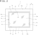
- the sealing resin part 5 is formed in a frame shape along the rectangular outer shape of the substrate 2 in plan view and has four side parts 5a along the respective sides of the rectangular outer shape of the substrate 2 as depicted in FIG. 2 .
- the sealing resin part 5 has side surface parts 5c continuous with the side surfaces 2c of the substrate 2 in such a manner as to be flush with the side surfaces 2c of the substrate 2.
- the sealing resin part 5 is formed by curing a resin material around the image sensor 3 on the substrate 2 and the glass 4 in a configuration in which the image sensor 3 is mounted on the substrate 2, these are connected to each other by the bonding wires 7, and the glass 4 is mounted on the image sensor 3 through the support part 6.
- the sealing resin part 5 is formed into a predetermined shape by injection molding using, for example, a molding mold.
- the sealing resin part 5 may be a part formed by a potting process using, for example, a dispenser. In this case, the resin material serving as the sealing resin part 5 is applied to a predetermined region while being discharged from the nozzle of the dispenser, and then cured to form the sealing resin part 5.
- the material of the sealing resin part 5 is, for example, a thermosetting resin containing silicon oxide as a main component or a filler such as alumina.
- a thermosetting resin such as a phenolic resin, a silicon-based resin, an acrylic resin, an epoxy resin, a urethane resin, a silicon resin, or a polyetheramide resin, a thermoplastic resin such as polyamide-imide, polypropylene, or liquid crystal polymer, a photosensitive resin such as a UV curable resin that is an acrylic resin, rubber, and other known resin materials are used singly or in combination.
- the sealing resin part 5 may be a part formed including a resin material in a liquid state at normal temperature by compression molding or the like. It should be noted that the sealing resin part 5 has an insulating property.
- the sealing resin part 5 is formed including a material having a light shielding property.
- a black resin material containing a black pigment such as carbon black or titanium black is used as a material of the sealing resin part 5. Accordingly, the sealing resin part 5 becomes a black part, and the sealing resin part 5 can function as a light shielding part.
- the sealing resin part 5 provided at the peripheral part on the substrate 2 in the imaging device 1 has a protrusion part 20.
- the protrusion part 20 is formed as a part of the sealing resin part 5 by, for example, injection molding, and an upper surface 21 is positioned above the front surface 4a of the glass 4 in the vertical direction that is the plate thickness direction of the substrate 2. That is, the protrusion part 20 is a part in the sealing resin part 5 protruding upward from the front surface 4a of the glass 4.
- the upper surface 21 of the protrusion part 20 is a surface perpendicular to the vertical direction.
- the protrusion part 20 is positioned on a common horizontal virtual plane A1.
- the protrusion part 20 has a constant or substantially constant protrusion height h1 from the front surface 4a of the glass 4.
- the protrusion part 20 is formed so as to surround the whole circumference of the glass 4 along the plan view outer shape of the sealing resin part 5.
- the protrusion part 20 has four side parts 20a along the rectangular outer shape of the glass 4 in plan view and is formed in a frame shape in plan view by these side parts 20a (see FIG. 2 ).
- the four side parts 20a are linear parts along the sides of the glass 4, and the width w1 is made constant or substantially constant as a whole.
- Each side part 20a of the protrusion part 20 serves as an upper surface layer part of each side part 5a in the sealing resin part 5.
- the protrusion part 20 is formed at a position slightly outside the four side surfaces 4c of the glass 4.
- the protrusion part 20 has an inner peripheral-side upper surface part 22 that is continuous with the front surface 4a of the glass 4 in such a manner as to be flush therewith and an inner surface part 23 that is an opposite surface of each of the four side surface parts 5c in the sealing resin part 5.
- the protrusion height h1 which is the dimension between the front surface 4a of the glass 4 and the upper surface 21 of the protrusion part 20, in the vertical direction is, for example, 10 to 200 ⁇ m. It should be noted that the thickness of the glass 4 is approximately 400 ⁇ m to 500 ⁇ m, as an example.
- the width w1 of each side part 20a of the protrusion part 20 is, for example, 100 ⁇ m or more.
- the width w1 of the side part 20a is, for example, a value within the range of 100 to 150 ⁇ m, a value within the range of 100 to 200 ⁇ m, a value within the range of 100 to 250 ⁇ m, or a value within the range of 100 to 300 ⁇ m.
- the chip size of the imaging device 1 one side of the square has, for example, 6 to 10 mm.
- a step of preparing the substrate 2 is performed.
- the substrate 2 is obtained, for example, by dicing and singulating a substrate member in which a plurality of substrate parts serving as the substrate 2 in the imaging device 1 is two-dimensionally connected.
- the plurality of lead terminals 13 is formed on the front surface 2a of the substrate 2.
- a step of preparing the image sensor 3 as an imaging element mounted on the substrate 2 is performed.
- the plurality of electrode pads 14 is formed through plating or the like.
- a step of preparing the glass 4 as a transparent member mounted on the image sensor 3 is performed.
- the glass 4 is obtained, for example, by cutting a glass plate having a predetermined shape into a rectangular shape by dicing.
- an assembly step is performed.
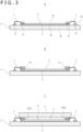
- a step of mounting the image sensor 3 on the substrate 2 is first performed. That is, die bonding of the image sensor 3 to the substrate 2 is performed.
- the image sensor 3 is bonded to a predetermined mounting region on the front surface 2a of the substrate 2 by a die bond material such as an insulating or conductive resin paste that serves as the joint layer 9.
- a step of providing the bonding wires 7 for electrically connecting the substrate 2 and the image sensor 3 to each other is performed.
- wire bonding is performed in which the lead terminals 13 of the substrate 2 and the electrode pads 14 of the image sensor 3 are electrically connected to each other by the bonding wires 7.
- a step of providing the glass 4 on the image sensor 3 through the support part 6 is performed. Specifically, first, as depicted in FIG. 3B , a rib resin 31, which is a resin material serving as the support part 6, is applied to a predetermined region on the front surface 3a of the image sensor 3 by a dispenser or the like in a rectangular frame shape along the outer shape of the image sensor 3 in plan view.
- the rib resin 31 may be formed by patterning through photolithography or the like.
- a step of mounting the glass 4 is performed.
- the glass 4 is mounted on the image sensor 3 so as to close an opening on the upper side of the rib resin 31.
- a step of curing the rib resin 31 on the front surface 3a of the image sensor 3 is performed.
- a heating step (cure) for curing the rib resin 31 is performed in a state where the glass 4 is mounted on the image sensor 3 through the rib resin 31.
- a step of pasting a protective sheet 40 as a protective material to the front surface 4a of the glass 4 is performed.
- the protective sheet 40 has substantially the same shape and dimensions as the front surface 4a of the glass 4 and is pasted so as to cover the whole front surface 4a of the glass 4.
- the protective sheet 40 for example, a sheet having adhesiveness and heat resistance such that the covering state of the front surface 4a for the glass 4 can be maintained in injection molding for forming the sealing resin part 5 is used.
- a sheet having a thickness equal to the dimension of the protrusion height h1 (see FIG. 1 ) of the protrusion part 20 in the sealing resin part 5 of the imaging device 1 or a thickness larger than the dimension of the protrusion height h1 is used.
- the protective sheet 40 that is a film-like member that wholly covers the front surface 4a of the glass 4 is used as a protective material.
- the protective sheet 40 has a base material 41 formed by a predetermined material and an adhesive layer 42 including an adhesive material for pasting the base material 41 to the glass 4. That is, the material configuration of the protective sheet 40 is a two-layer structure including the base material 41 and the adhesive layer 42. Regarding the thickness of each layer of the protective sheet 40, the layer thickness T1 of the base material 41 is thicker than the layer thickness T2 of the adhesive layer 42. However, the size relation between the layer thicknesses of the base material 41 and the adhesive layer 42 is not limited.
- a predetermined material for forming the base material 41 is, for example, an organic-based film material.
- PET polyethylene terephthalate
- the adhesive layer 42 a material that can adhere to the base material 41 and can easily clean, even in a case where a glue residue (residue of an adhesive) occurs on the glass 4 as an adherend, the residue with an organic solvent or the like is used.
- an acrylic resin adhesive is used as a material of the adhesive layer 42.
- the base material 41 is assumed to be formed by PET, and the adhesive layer 42 is assumed to be formed by an acrylic resin adhesive.
- the layer structure of the protective sheet 40 and the material of each layer are not limited.
- the material of the adhesive layer 42 is a thermosetting resin
- a step of curing the adhesive layer 42 is performed to fix the protective sheet 40 to the front surface 4a of the glass 4.
- the protective sheet 40 may have a single layer or a laminated structure of three or more layers.
- the steps including the step of providing the glass 4 on the image sensor 3 and the step of pasting the protective sheet 40 to the front surface 4a of the glass 4 are the step of providing, on the image sensor 3 through the support part 6, the glass 4 with the front surface 4a covered with the protective sheet 40.
- the glass 4 with the protective sheet 40 pasted to the front surface 4a in advance may be used.
- the glass 4 with the protective sheet 40 is prepared.
- the glass 4 with the protective sheet 40 is obtained in such a manner that the protective sheet is wholly pasted to the front surface of a glass plate in a wafer state before being singulated into the glass 4 in a chip state and the glass plate is then singulated together with the protective sheet.
- the two-layer structure of the base material 41 formed by PET and the adhesive layer 42 of an acrylic resin adhesive as described above, or, for example, a DAF material (DAF: die attach film) used for bonding a semiconductor chip to a substrate, or the like can be used.
- DAF material die attach film
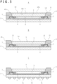
- the step of providing, on the image sensor 3 through the support part 6, the glass 4 with the front surface 4a covered with the protective sheet 40 is as follows. That is, after the rib resin 31 is applied onto the front surface 3a of the image sensor 3 as depicted in FIG. 3B , the glass 4 with the protective sheet 40 is mounted as depicted in FIG. 4A , and a curing step for curing the rib resin 31 is performed. By using the glass 4 with the protective sheet 40, the step of pasting the protective sheet 40 to the glass 4 provided on the image sensor 3 is omitted.
- a step of forming the sealing resin part 5 around the image sensor 3 on the substrate 2 and the glass 4 is performed by use of a mold 50 for molding the molding resin part.
- the mold 50 has an upper mold 51 that is a first mold, and a lower mold 52 that is a second mold for forming a cavity 53 which is a molding space together with the upper mold 51.
- the upper mold 51 has a flat molding surface 51a for forming the upper side of the sealing resin part 5.
- the lower mold 52 has a flat support surface 52a, as a surface for supporting the substrate 2, facing the molding surface 51a of the upper mold 51 in a parallel manner.
- the mold 50 is a transfer mold and has a pot (not depicted) in which a tablet that is a solid resin of a molding material is set, and a plunger (not depicted) driven in the pot.
- the space in the pot communicates with the cavity 53 through a gate or the like serving as a passage for the resin material.
- the molding surface 51a of the upper mold 51 is wholly covered with a film 55 formed by an elastic or plastic material.
- the film 55 is what is generally called a release film, and is, for example, automatically supplied from a supply device attached to the mold 50 and comes into close contact with the molding surface 51a of the upper mold 51 by vacuum suction or the like.
- the film 55 is peeled off from the molding surface of the upper mold 51 each time the mold 50 is opened and the molded article is taken out, and is supplied for each shot of injection molding.
- a resin material 5X forming the sealing resin part 5 is prevented from adhering to the molding surface 51a of the upper mold 51.
- the thickness of the film 55 is, for example, approximately 200 ⁇ m.
- a workpiece subjected to the formation of the sealing resin part 5 is set to such a mold 50. It should be noted that the workpiece has the configuration depicted in FIG. 4A . As depicted in FIG. 4B , the workpiece is set in a state where it is placed at a predetermined position on the support surface 52a of the lower mold 52 in a direction in which the protective sheet 40 side is the upper mold 51 side and the substrate 2 side is the lower mold 52 side.
- the mold 50 After the workpiece is set to the mold 50, the mold 50 becomes a mold closed state (mold clamped state), so that the cavity 53 is formed.
- the mold closed state of the mold 50 the workpiece becomes a clamped state in which it is vertically sandwiched between the lower mold 52 and the upper mold 51.
- the film 55 is pressed against the protective sheet 40 on the glass 4, and the protective sheet 40 comes into close contact with the film 55. That is, the protective sheet 40 is pressed against the molding surface 51a of the upper mold 51 from an upper surface 40a side through the film 55. Accordingly, the protective sheet 40 is compressed in the thickness direction according to the thickness thereof and slightly expanded in the surface direction.
- the tablet in the pot is melted and pumped in a predetermined passage as the resin material 5X and injected and filled into the cavity 53.
- a black resin material having a light shielding property is used as the resin material 5X by containing, for example, a black pigment such as carbon black or titanium black.
- the resin material 5X is not limited to the material having a light shielding property.
- the resin material 5X is cured by performing a predetermined process such as heating or cooling the resin material 5X. Accordingly, a resin part serving as the sealing resin part 5 is formed. Thereafter, the clamp by the mold 50 is released, the mold 50 is opened, and the workpiece subjected to injection molding is taken out.
- the protective sheet 40 in the workpiece taken out from the mold 50, the protective sheet 40 remains on the glass 4.
- the upper surface 40a of the protective sheet 40 is flush with the upper surface 21 of the sealing resin part 5 by the molding surface 51a of the upper mold 51 in a horizontal state.
- the thickness of the protective sheet 40 may become thicker than that in the clamped state due to the return of the protective sheet 40 from the compressed state caused by the release of the clamp by the mold 50, or the protective sheet 40 may be deformed from the wholly pasted state to the front surface 4a of the glass 4.
- a step of removing the protective sheet 40 is performed.
- the protective sheet 40 on the glass 4 is peeled off by being picked up, for example, by a suction collet or the like.
- the residue is cleaned by use of, for example, an organic solvent.
- the protrusion part 20 By removing the protective sheet 40, the front surface 4a of the glass 4 whose periphery is surrounded by the sealing resin part 5 is exposed. Then, in the sealing resin part 5, the part surrounding the periphery of the protective sheet 40 serves as the protrusion part 20. That is, the horizontal molding surface 51a is filled with the resin material 5X above the front surface 4a of the glass 4 by the thickness of the protective sheet 40, and the part above the front surface 4a of the glass 4 serves as the protrusion part 20 in the sealing resin part 5.
- the protrusion height h1 (see FIG. 1 ) of the protrusion part 20 has the same or substantially the same dimension as the thickness of the protective sheet 40.
- the glass 4 and the sealing resin part 5 form a recess part having the front surface 4a of the glass 4 and the inner peripheral-side upper surface part 22 as a bottom surface part and the four inner surface parts 23 as side surfaces.
- the peripheral part of the lower surface 40b of the protective sheet 40 serves as a surface forming the inner peripheral-side upper surface part 22, and the side surfaces 40c of the protective sheet 40 serve as surfaces forming the inner surface parts 23.
- a step of providing the plurality of solder balls 15 on the rear surface 2b side of the substrate 2 is performed.
- a step of ball mounting and reflow is performed in which solder is arranged and fixed to each of the plurality of terminal electrodes arranged and formed in a lattice point shape on the rear surface 2b side of the substrate 2.
- the protective sheet 40 pasted to the glass 4.
- the protective sheet 40 has a substantially rectangular plan view outer shape corresponding to the front surface 4a of the glass 4 and has recess parts 46 formed on four side parts 45 in the outer shape in plan view, and R-shaped parts 48 formed at four corner parts 47.
- the recess part 46 is a curved recess part with respect to a rectangular virtual outer shape V1 corresponding to the outer shape of the glass 4 in plan view.
- the recess part 46 is formed in the middle part excluding both ends in each side part 45 of the protective sheet 40.
- the recess part 46 is formed so as to form, for example, an arc shape.
- the protective sheet 40 has a shape constricted by the recess parts 46 on four sides facing each other in the longitudinal direction (the lateral direction in FIG. 7 ) and the short-length direction (the vertical direction in FIG. 7 ). That is, in the regions where the recess parts 46 are formed, the width gradually narrows from both ends to the central part in each direction of the longitudinal direction and the short-length direction of the protective sheet 40. It should be noted that the protective sheet 40 has a symmetrical or substantially symmetrical shape in each direction of the longitudinal direction and the short-length direction.
- the protective sheet 40 is formed such that a recess amount D1 of the recess part 46 with respect to a virtual straight line V1a that is each side of the virtual outer shape V1 has a predetermined dimension.
- the recess amount D1 is a distance between each virtual straight line V1a and a vertex P1 positioned in the center of the recess part 46 in each direction of the longitudinal direction and the short-length direction of the protective sheet 40.
- the recess amount D1 of the recess part 46 can be determined on the basis of, for example, the layer thickness T2 (see FIG. 6 ) of the adhesive layer 42 of the protective sheet 40. Specifically, the recess amount D1 of the recess part 46 with respect to the virtual straight line V1a along the rectangular shape in the outer shape of the protective sheet 40 in plan view is set as a dimension 0.7 to 1.3 times the layer thickness T2 of the adhesive layer 42. However, the magnitude of the recess amount D1 of the recess part 46 is not limited to values within the numerical range described above.
- the recess amounts D1 on the long side and the short side of the protective sheet 40 may be different from each other.
- the recess amount D1 of the recess part 46 (46B) on the short side of the protective sheet 40 may be set longer than the recess amount D1 of the recess part 46 (46A) on the long side.
- the shape of the recess part 46 is not limited to an arc shape, and is only required to be a shape in which the protective sheet 40 is constricted in the longitudinal direction and the short-length direction as a pair of recess parts 46 of the protective sheet 40 facing each other in the longitudinal direction or the short-length direction.
- the R-shaped part 48 is a rounded shape part formed to have an arc-shaped curve with respect to the right-angled corner part in the virtual outer shape V1.
- the protective sheet 40 is formed such that a curvature radius R1 of the arc formed by the R-shaped part 48 becomes a predetermined value.
- the curvature radius R1 of the R-shaped part 48 is set to a value of, for example, approximately 0.2 mm.
- the magnitude of the curvature radius R1 is not particularly limited.
- the curvature radiuses R1 of the four corner parts 47 in the protective sheet 40 may be different in magnitude for each corner part 47.
- the protective sheet 40 has the recess parts 46 and the R-shaped parts 48, and the protective sheet 40 may be only required to have at least any one of the recess parts 46 and the R-shaped parts 48.
- the recess parts 46 may be formed only on a part of the side parts 45 among the four side parts 45 of the protective sheet 40, such as, for example, being formed only on a set of side parts 45 facing each other in the protective sheet 40.
- the R-shaped parts 48 may be formed only at a part of the corner parts 47 among the four corner parts 47 of the protective sheet 40.
- the imaging device 1 and the manufacturing method thereof according to the present embodiment as described above it is possible to suppress the occurrence of scratches and stains on the glass 4 provided so as to cover the image sensor 3 from the front surface 3a side and to stabilize the manufacturing yield. Since the imaging device 1 has the protrusion part 20 in the sealing resin part 5, the protrusion part 20 can be a part subjected to the suction action by the collet when being picked up by the collet, so that it is possible to suppress the occurrence of scratches and stains on the glass 4 by the collet.
- the front surface 4a of the glass 4 becomes the uppermost surface in the package structure.
- an upper surface 5s of the sealing resin part 5 becomes a surface having substantially the same height as the front surface 4a of the glass 4 or lower than the front surface 4a of the glass 4.
- the glass 4 slightly bites into the film 55, so that the upper surface 5s of the sealing resin part 5 becomes a surface lower than the front surface 4a of the glass 4.
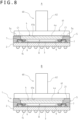
- the package of the comparative example is subjected to the suction action by a collet 60 on the front surface 4a of the glass 4 when being picked up by the collet 60.
- the collet 60 is what is generally called a flat collet and has a rectangular plate-like holding part 61 for sucking and holding an object to be picked up, and a columnar support part 62 for attaching the collet 60 to the main body side of the pickup device.
- the holding part 61 has a suction surface 61a along a plane and brings the suction surface 61a into contact with the suction object.
- An intake passage formed in communication from the support part 62 to the holding part 61 faces and opens in the suction surface 61a. On the suction surface 61a, the suction action by a suction device provided on the main body side of the device is obtained by the intake passage.
- the suction surface 61a of the collet 60 interferes with the glass 4, especially the corner parts on the front surface 4a side (see the parts indicated by the symbol C1), and there is a risk that the glass 4 is scratched or that the stains of the collet 60 adhere to the glass 4 to contaminate the glass 4.
- the occurrence of scratches and contamination in the glass 4 causes a decrease in the manufacturing yield.
- the imaging device 1 of the embodiment since the sealing resin part 5 has the protrusion part 20 with the upper surface 21 positioned above the front surface 4a of the glass 4, the upper surface 21 of the sealing resin part 5 becomes the uppermost surface in the imaging device 1. Therefore, when being picked up by the collet 60, the imaging device 1 is subjected to the suction action by the collet 60 by contact of the suction surface 61a with the upper surface 21 of the sealing resin part 5.
- a flat collet such as the collet 60 depicted in FIG. 8B can be used. Accordingly, it is not necessary to use a dedicated collet according to the size or the like of the glass 4 as a collet for picking up the imaging device 1, and an increase in cost can be avoided.
- the dimension of the protrusion height h1 is preferably within the range of 10 to 200 ⁇ m for the following reasons. That is, if the protrusion height h1 of the protrusion part 20 is less than 10 ⁇ m, the height of the upper surface 21 of the sealing resin part 5 with respect to the front surface 4a of the glass 4 becomes insufficient, and it becomes difficult to prevent the collet 60 from interfering with the glass 4.
- the protrusion height h1 of the protrusion part 20 exceeds 200 ⁇ m, the shrinkage stress of the sealing resin part 5 increases, and the shrinkage stress may cause an adverse effect on other configurations configuring the imaging device 1.
- the protrusion height h1 of the protrusion part 20 exceeds 200 ⁇ m, the amount of the resin material forming the sealing resin part 5 increases, and thus there is a problem of increasing the cost.
- the protrusion height h1 of the protrusion part 20 exceeds 200 ⁇ m, the protrusion part 20 existing around the glass 4 becomes high, and thus, the incident light to the glass 4 easily hits the protrusion part 20.
- the incident light hits the inner surface part 23 of the protrusion part 20
- the reflected light from the inner surface part 23 enters the image sensor 3, and thus, there is a possibility that the flare is generated or deteriorated.
- the protrusion part 20 becomes high, there is a possibility of causing a problem that the incident light to the image sensor 3 is blocked by the protrusion part 20.
- the width w1 (see FIG. 1 ) of each side part 20a of the protrusion part 20 is preferably 100 ⁇ m or more for the following reasons. That is, by securing 100 ⁇ m or more for the width w1 of each side part 20a of the protrusion part 20, it is possible to secure a sufficient area for the upper surface 21 of the sealing resin part 5 with which the suction surface 61a of the collet 60 is brought into contact. Accordingly, the suction action by the collet 60 can be sufficiently obtained, and the suction of the imaging device 1 by the collet 60 can be facilitated, so that an excellent pickup property for the imaging device 1 can be obtained.
- the manufacturing method of the imaging device includes the step of providing, on the upper side of the image sensor 3, the glass 4 with the front surface 4a covered with the protective sheet 40 in the step of injection molding for forming the sealing resin part 5. That is, the manufacturing method according to the present embodiment uses the protective sheet 40 covering the front surface 4a of the glass 4 to form the protrusion part 20 in the sealing resin part 5.
- the protective sheet 40 by using the protective sheet 40, it is not necessary to form the mold in a complicated shape in order to form the protrusion part 20 in the sealing resin part 5, and the protrusion part 20 can be formed by using the existing mold having the flat molding surface 51a. Accordingly, the manufacturing cost of the imaging device 1 can be suppressed.
- the protective sheet 40 it is possible to suppress the occurrence of stains and scratches on the front surface 4a of the glass 4 by injection molding for forming the sealing resin part 5. Accordingly, it is possible to stabilize the manufacturing yield.
- the resin material can be dammed by the protective sheet 40 in injection molding, and it is possible to suppress the occurrence of burrs due to riding of the resin material on the front surface 4a of the glass 4. That is, it is possible to suppress the occurrence of burrs and bleeds caused by the infiltration of the resin material between the front surface 4a of the glass 4 and the film 55 on the upper mold 51 side due to variations in the flatness of the glass 4 or the like in a case where the protective sheet 40 is not used.
- the protective sheet 40 that is peeled off and removed in the manufacturing process, even in a case where burrs or the like occur on the protective sheet 40, it is possible to remove the burrs or the like together with the protective sheet 40 at the same time when the protective sheet 40 is peeled off.
- the protective sheet 40 damage to the glass 4 or the like caused by the clamping pressure of the mold 50 can be avoided.
- the manufacturing yield can be stabilized even by enabling suppression of the occurrence of burrs and the like and avoidance of damage to the glass 4 or the like as described above.
- the manufacturing method of the imaging device includes the step of removing the protective sheet 40 after the step of injection molding for forming the sealing resin part 5 using the protective sheet 40 as a film-like member. According to such a manufacturing method, the front surface 4a of the glass 4 can be maintained in a clean state, and the performance of the imaging device 1 can be secured.
- the manufacturing method of the imaging device uses the protective sheet 40 having the recess parts 46 formed on the four side parts 45 and the R-shaped parts 48 formed at the four corners.
- the shape of the mold 50 after deformation by clamping can be approximated to a rectangular shape corresponding to the shape of the glass 4 in plan view.
- the four side parts 45 are deformed so as to swell outward (see the arrows F1), and the corner parts 47 are deformed so as to project outward at the four corners (see the arrows F2).
- the corner parts 47 are deformed so as to project outward at the four corners (see the arrows F2).
- these deformations for example, in a case where the protective sheet 40 has the virtual outer shape V1, a part of the protective sheet 40 is deformed to protrude outward with respect to the virtual outer shape V1.
- the protective sheet 40 having the shape in plan view as depicted in FIG. 7 , for the deformation caused by the clamping of the mold 50, the deformation caused on the side parts 45 is offset by the recess parts 46, and the side parts 45 are approximated to the shape along the virtual straight line V1a.
- the deformation generated at the corner parts 47 is offset by the R-shaped parts 48, and the corner parts 47 are approximated to the shapes along the right-angled corner parts of the virtual outer shape V1.
- the recess amount D1 of the recess part 46 is preferably within the range of 0.7 to 1.3 times the layer thickness T2 of the adhesive layer 42. Accordingly, the shape of the protective sheet 40 in the deformed state by clamping of the mold 50 can effectively be approximated to a rectangular shape (virtual outer shape V1). In addition, by allowing the curvature radius R1 of the R-shaped part 48 to be approximately 0.2 mm, the shape of the protective sheet 40 in the deformed state can effectively be approximated to a rectangular shape.
- the manufacturing method of the imaging device according to the present embodiment uses a two-layer structure of the base material 41 and the adhesive layer 42 as the protective sheet 40.
- the protective sheet 40 can have a simple and inexpensive configuration.
- the protective sheet 40 As a preferred configuration of the protective sheet 40, a configuration in which the material of the base material 41 is PET and the material of the adhesive layer 42 is an acrylic resin adhesive is employed. Accordingly, it is possible to obtain excellent adhesion of the adhesive layer 42 to the base material 41, and to easily and safely clean the adhesive layer 42 remaining on the front surface 4a of the glass 4 after peeling off the protective sheet 40 by using an organic solvent. That is, it is possible to obtain excellent adhesiveness and removability of the protective sheet 40 to the front surface 4a of the glass 4.
- FIG. 9 A configuration example of an imaging device 71 according to a second embodiment of the present technique will be described with reference to FIG. 9 and FIG. 10 .
- the same reference signs are given to the common configurations as in the first embodiment, and description of the duplicate contents is appropriately omitted.
- the imaging device 71 according to the present embodiment differs from the imaging device 1 according to the first embodiment in terms of the structure of the protrusion part 20 of the sealing resin part 5. That is, in the imaging device 71 according to the present embodiment, the protrusion part 20 has a glass covering part 25 as a transparent member covering part that extends on the front surface 4a of the glass 4 so as to cover an edge part of the front surface 4a of the glass 4.
- the glass covering part 25 is a part of the protrusion part 20 that extends inward along the front surface 4a of the glass 4 while maintaining the height of the upper surface 21 from the main body part of the protrusion part 20.
- the dimension (thickness) of the glass covering part 25 in the vertical direction is constant or substantially constant as a whole.
- the glass covering part 25 is formed over the whole circumference of the edge part of the front surface 4a of the glass 4 along the outer shape of the glass 4 in plan view.
- the glass covering part 25 has four side parts 25a along the outer shape of the glass 4 in plan view and is formed in a frame shape in plan view by these side parts 25a (see FIG. 10 ).
- the four side parts 25a are linear parts along the sides of the glass 4, and the width thereof is constant or substantially constant as a whole.
- the side parts 25a of the glass covering part 25 are inner peripheral parts of the side parts 20a of the protrusion part 20.
- the glass covering part 25 forms the inner peripheral side of the upper surface 21 of the sealing resin part 5 by the upper surface thereof and has a lower surface 25b that is a contact surface with the front surface 4a of the glass 4 and an end surface 25c on the inner peripheral side.
- the glass covering part 25 is formed in a region outside the pixel region 12 so as not to overlap the pixel region 12 of the image sensor 3 in plan view. That is, the glass covering part 25 is formed such that the end surface 25c on the inner peripheral side is positioned outside the pixel region 12.
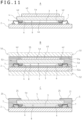
- die bonding and wire bonding are performed (see FIG. 3A ), and the step of providing, on the image sensor 3 through the support part 6, the glass 4 with the front surface 4a covered with the protective sheet 40 is performed (see FIG. 3B, FIG. 3C , and FIG. 4A ).
- a sheet having an outer dimension a little smaller than that of the glass 4 is used as the protective sheet 40. That is, the protective sheet 40 partially covers the front surface 4a of the glass 4 except a peripheral edge part of the front surface 4a. A part of the front surface 4a of the glass 4 that is not covered with the protective sheet 40, that is, an exposed part 4d of a peripheral edge of the front surface 4a serves as a formation region of the glass covering part 25. It should be noted that the magnitude of the protective sheet 40 is set in consideration of an increase (spread) in the area of the protective sheet 40 due to compression by clamping of the mold 50.
- the step of forming the sealing resin part 5 is performed by injection molding with use of the mold 50.
- the resin material 5X enters between the film 55 on the upper mold 51 side and the exposed part 4d of the front surface 4a of the glass 4 around the protective sheet 40 to form the glass covering part 25.
- a step of removing the protective sheet 40 is performed as depicted in FIG. 11C .
- the step of providing a plurality of solder balls 15 on the rear surface 2b side of the substrate 2 is performed (see FIG. 5C ).
- the imaging device 71 of the second embodiment in addition to the effect obtained by the first embodiment, the following effect can be obtained. That is, with a configuration in which the protrusion part 20 of the sealing resin part 5 has the glass covering part 25 covering the glass 4, the sealing resin part 5 can have a function as a light shielding film for cutting unnecessary light.
- the sealing resin part 5 is preferably formed by a material having a light shielding property such as a black resin material containing a black pigment.
- a light shielding function can be obtained in the glass 4 without using, for example, a glass with a relatively expensive light shielding film. Accordingly, the member cost can be suppressed.
- FIG. 12 and FIG. 13 A configuration example of an imaging device 81 according to a third embodiment of the present technique will be described with reference to FIG. 12 and FIG. 13 .
- the imaging device 81 according to the present embodiment differs from the imaging device 71 according to the second embodiment in that a sealing resin receiving part 82 is provided on the front surface 4a of the glass 4 at a region inside the sealing resin part 5.
- the sealing resin receiving part 82 is provided at the edge part on the front surface 4a of the glass 4 and is in contact with the protrusion part 20 at an outer surface 83 that is an outer side surface.
- the sealing resin receiving part 82 is formed over the whole circumference of the edge part of the front surface 4a of the glass 4 along the outer shape of the glass 4 in plan view.
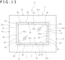
- the sealing resin receiving part 82 has four side parts 82a along the outer shape of the glass 4 in plan view and is formed in a frame shape in plan view by these side parts 82a (see FIG. 13 ).
- the four side parts 82a are linear parts along the sides of the glass 4, and the width thereof is constant or substantially constant as a whole.
- the dimension (thickness) of the sealing resin receiving part 82 in the vertical direction is constant or substantially constant as a whole.
- the sealing resin receiving part 82 has, for example, a rectangular transverse cross-sectional shape at each side part 82a.
- the sealing resin receiving part 82 has the outer surface 83, an inner surface 84 that is a side surface on the opposite side (inner side) of the outer surface 83, an upper surface 85, and a lower surface 86 that a contact surface with the front surface 4a of the glass 4.
- the upper surface 85 of the sealing resin receiving part 82 is flush with the upper surface 21 of the sealing resin part 5.
- the sealing resin receiving part 82 is formed in a region outside the pixel region 12 so as not to overlap the pixel region 12 of the image sensor 3 in plan view. That is, the sealing resin receiving part 82 is formed such that the inner surface 84 is positioned outside the pixel region 12.
- the sealing resin receiving part 82 is formed at a region slightly inside an edge of the front surface 4a of the glass 4. Therefore, the glass covering part 25 of the protrusion part 20 is formed at an edge end part of the front surface 4a of the glass 4. That is, the sealing resin receiving part 82 is surrounded by the glass covering part 25. The sealing resin receiving part 82 is in contact with the inner end surface 25c of the glass covering part 25 on the outer surface 83.
- the material for forming the sealing resin receiving part 82 is not particularly limited, and is, for example, a photosensitive adhesive such as a UV (ultraviolet) curable resin that is an acrylic resin, a thermosetting resin such as an epoxy resin, or a mixture thereof.
- the material for forming the sealing resin receiving part 82 is preferably a material having a light shielding property such as a black resin material containing a black pigment such as carbon black.
- the sealing resin receiving part 82 is formed on the front surface 4a of the glass 4 by coating with a dispenser, patterning through photolithography, or the like.
- the sealing resin receiving part 82 may be formed by pasting the protective sheet 40 used in the first embodiment and the like to the front surface 4a of the glass 4 as a frame shape. It should be noted that the sealing resin receiving part 82 is not limited to those including resin, and may be provided by pasting, for example, a structure including ceramics such as glass or an inorganic material such as metal or silicon to the glass 4 with an adhesive or the like.
- die bonding and wire bonding are performed (see FIG. 3A ), and the step of providing the glass 4 on the image sensor 3 through the support part 6 is performed (see FIG. 3B and FIG. 3C ).
- a step of forming the sealing resin receiving part 82 as a protective material on the front surface 4a of the glass 4 is performed.
- a rib resin 82X which is a resin material serving as the sealing resin receiving part 82, is applied to a predetermined region on the front surface 4a of the glass 4 by a dispenser or the like in a rectangular frame shape along the outer shape of the glass 4 in plan view.
- the rib resin 82X may be formed by patterning through photolithography, or the like.
- a step of curing the rib resin 82X on the front surface 4a of the glass 4 is performed.
- a heating step (cure) for curing the rib resin 82X is performed in a state where the rib resin 82X is applied to the front surface 4a of the glass 4.
- the sealing resin receiving part 82 is formed on the glass 4 by the rib resin 82X.
- the sealing resin receiving part 82 is formed at a region slightly inside the edge of the front surface 4a of the glass 4. Therefore, the exposed part 4d is present on the front surface 4a of the glass 4 outside the sealing resin receiving part 82, and the exposed part 4d serves as a formation region of the glass covering part 25.
- the sealing resin receiving part 82 may be provided at the edge of the front surface 4a of the glass 4 such that the exposed part 4d of the front surface 4a of the glass 4 is not present outside the sealing resin receiving part 82.
- a portion on the front surface 4a of the glass 4 inside the sealing resin receiving part 82 is exposed.
- the sealing resin receiving part 82 for example, a sheet having heat resistance such that the fixing state to the front surface 4a of the glass 4 can be maintained in injection molding for forming the sealing resin part 5 is used.
- a sheet having a thickness equal to the dimension of the protrusion height h1 (see FIG. 1 ) of the protrusion part 20 in the sealing resin part 5 of the imaging device 81 or a thickness larger than the dimension of the protrusion height h1 is used.
- the sealing resin receiving part 82 covering the peripheral edge part of the front surface 4a of the glass 4 is used as a protective material.
- the steps including the step of providing the glass 4 on the image sensor 3 and the step of providing the sealing resin receiving part 82 on the front surface 4a of the glass 4 are the step of providing, on the image sensor 3 through the support part 6, the glass 4 with the peripheral edge part of the front surface 4a covered with the sealing resin receiving part 82.
- the glass 4 with the sealing resin receiving part 82 provided on the front surface 4a in advance may be used.
- the glass 4 with the sealing resin receiving part 82 is prepared.
- the glass 4 with the sealing resin receiving part 82 is obtained in such a manner that, on the front surface of a glass plate in a wafer state before being singulated into chip-shaped glasses, the sealing resin receiving part 82 is provided for each region corresponding to each glass 4 and the glass plate is then singulated.
- the step of providing, on the image sensor 3 through the support part 6, the glass 4 with the peripheral edge part of the front surface 4a covered with the sealing resin receiving part 82 is as follows. That is, after the rib resin 31 is applied onto the front surface 3a of the image sensor 3 (see FIG. 3B ), the glass 4 with the sealing resin receiving part 82 is mounted as depicted in FIG. 11A , and a curing step for curing the rib resin 31 is performed. By using the glass 4 with the sealing resin receiving part 82, the step of providing the sealing resin receiving part 82 on the glass 4 provided on the image sensor 3 is omitted.
- the step of forming the sealing resin part 5 is performed by injection molding with use of the mold 50.
- the sealing resin receiving part 82 has elasticity or plasticity
- the sealing resin receiving part 82 is compressed by clamping the workpiece by use of the mold 50.
- the resin material 5X enters between the film 55 on the upper mold 51 side and the exposed part 4d of the front surface 4a of the glass 4 around the sealing resin receiving part 82 to form the glass covering part 25.
- the workpiece taken out from the mold 50 has a configuration having the sealing resin part 5 including the protrusion part 20 and the sealing resin receiving part 82 as depicted in FIG. 14C .
- the step of providing a plurality of solder balls 15 on the rear surface 2b side of the substrate 2 is performed (see FIG. 5C ).
- the imaging device 81 including the sealing resin part 5 having the glass covering part 25 in the protrusion part 20 and the sealing resin receiving part 82 is obtained. It should be noted that, in a case where the sealing resin receiving part 82 is provided at the edge of the front surface 4a of the glass 4, the glass covering part 25 is not formed in the protrusion part 20.
- the imaging device 81 of the third embodiment and the manufacturing method thereof in addition to the effects obtained by the first embodiment and the second embodiment, the following effect can be obtained. That is, by using the sealing resin receiving part 82 as a protective material provided on the front surface 4a of the glass 4 in order to form the protrusion part 20, the step of removing the protective material after forming the sealing resin part 5 can be omitted. Accordingly, the steps can be simplified.
- the sealing resin receiving part 82 can have a function as a light shielding film for cutting unnecessary light.
- the sealing resin receiving part 82 is preferably formed by a material having a light shielding property such as a black resin material containing a black pigment.
- a fourth embodiment of the present technique will be described with reference to FIG. 15 and FIG. 16 .
- the present embodiment is an embodiment for a manufacturing method of an imaging device and will be described by taking the imaging device 1 of the first embodiment as an example.
- a liquid resin 5Y that is a resin material in a liquid state at normal temperature is used as a resin material for forming the sealing resin part 5.
- a resin such as a UV (ultraviolet) curable resin or a thermosetting resin that can be cured by post-treatment is used.
- a mold 90 used for forming the sealing resin part 5 is what is generally called a compression molding mold and has an upper mold 91 that is a first mold, and a lower mold 92 that is a second mold forming a cavity 93 which is a molding space, together with the upper mold 91.
- the upper mold 91 has a rectangular recess part 91a for holding a workpiece 97 on the molding surface side.
- the recess part 91a has a shape and a dimension substantially the same as those of the substrate 2 in terms of the outer shape in plan view and has a depth substantially the same as the thickness of the substrate 2.
- the workpiece 97 is held under suction by the upper mold 91 in a state where the substrate 2 is fitted into the recess part 91a.
- an intake passage opened against the recess part 91a is provided, and the suction action by a suction device, which is not depicted, is obtained.
- the periphery of the recess part 91a is a flat mold alignment surface 91b with respect to the lower mold 92.
- the lower mold 92 has a rectangular recess part 92a at a position opposite to the recess part 91a of the upper mold 91 on the molding surface side.
- the recess part 92a has a shape and a dimension substantially the same as those of the recess part 91a of the upper mold 91 in terms of the outer shape in plan view and has a depth substantially the same as the height of the sealing resin part 5.
- the periphery of the recess part 92a is a flat mold alignment surface 92b with respect to the upper mold 91.
- the recess part 92a and the mold alignment surface 92b of the lower mold 92 are wholly covered with a buffer sheet 95 formed by an elastic or plastic material.
- the buffer sheet 95 functions as a buffer member and a release film, is automatically supplied from, for example, a supply device attached to the mold 90, and comes into close contact with the recess part 92a and the mold alignment surface 92b of the lower mold 92 by vacuum suction or the like.
- the buffer sheet 95 is peeled off from the molding surface of the lower mold 92 each time the mold 90 is opened and the molded article is taken out and is supplied for each shot of injection molding.
- the liquid resin 5Y forming the sealing resin part 5 is prevented from adhering to the recess part 92a and the mold alignment surface 92b of the lower mold 92.
- the thickness of the buffer sheet 95 is, for example, approximately 200 ⁇ m.
- the manufacturing method of the imaging device 1 according to the present embodiment is performed by the following procedure. First, as depicted in FIG. 15A , the liquid resin 5Y is supplied to the lower mold 92 in which the buffer sheet 95 is set to the recess part 92a and the mold alignment surface 92b. A prescribed amount of the liquid resin 5Y is applied into the recess part 92a of the lower mold 92 by a dispenser 96.
- the upper mold 91 with the workpiece 97 held under suction in the recess part 91a is set to the lower mold 92.
- the workpiece 97 is set upside down in the mold 90 with the substrate 2 side as the upper side. It should be noted that the workpiece 97 has a configuration in which the glass 4 with the front surface 4a covered with the protective sheet 40 is provided on the image sensor 3 (see FIG. 4A ).
- the upper mold 91 is lowered or the like to come close to the lower mold 92, and mold clamping of the mold 90 is performed.
- the mold 90 becomes a mold clamping state
- the cavity 93 corresponding to the shape of the sealing resin part 5 is formed, and the liquid resin 5Y is filled into the cavity 93 while being compressed.
- the buffer sheet 95 is sandwiched between the mold alignment surface 91b of the upper mold 91 and the mold alignment surface 92b of the lower mold 92, and the workpiece 97 is clamped between the upper and lower recess parts 91a and 92a.
- FIG. 16A is a partial enlarged view of E1 in FIG. 15C .
- a step of curing the liquid resin 5Y by UV irradiation, heating, or the like is performed, and the sealing resin part 5 is formed. Thereafter, the mold 90 is opened, and the workpiece 97 subjected to injection molding is taken out.
- the sealing resin part 5 is formed, and the protective sheet 40 remains on the glass 4.
- the level difference G1 is present between the upper surface 40a of the protective sheet 40 and the upper surface 21 of the sealing resin part 5, and a level difference part 98 from the sealing resin part 5 is formed around the protective sheet 40.
- a step of removing the protective sheet 40 is performed.
- a highly adhesive tape 99 is used to peel off the protective sheet 40 on the glass 4 (see an arrow H1).
- the residue is cleaned by use of, for example, an organic solvent.
- the protective sheet 40 When the protective sheet 40 is removed, as depicted in FIG. 16C , a configuration in which the sealing resin part 5 has the protrusion part 20 is obtained. Thereafter, the step of providing a plurality of solder balls 15 on the rear surface 2b side of the substrate 2 is performed (see FIG. 5C ).
- the imaging device 1 depicted in FIG. 1 and FIG. 2 can be obtained. It should be noted that the manufacturing method according to the present embodiment can also be applied as the manufacturing method of the imaging device 71 of the second embodiment and the imaging device 81 of the third embodiment.
- a resin material in a liquid state at normal temperature can be used as a material of the sealing resin part 5, it is possible to use a resin material having a physical property that is difficult to obtain with a solid resin such as a tablet used in, for example, injection molding.
- a resin having physical properties such as low elasticity, low Tg (Tg: glass transition temperature), and transparency.
- the level difference G1 can be formed between the upper surface 40a of the protective sheet 40 and the upper surface 21 of the sealing resin part 5. Accordingly, since the protective sheet 40 can easily be peeled off, an excellent peeling property of the protective sheet 40 can be obtained, and the step of removing the protective sheet 40 can easily be performed.
- the imaging device (solid-state imaging device) according to the present technique can be applied to an electronic apparatus in general that uses a solid-state imaging element for an image capturing part (photoelectric conversion part), such as a camera device, such as a digital still camera or a video camera, a portable terminal device having an imaging function, or a copying machine that uses a solid-state imaging element for an image reading part.
- the imaging device may be of a configuration formed as a single chip or may be of a module-like configuration having an imaging function in which an imaging part and a signal processing part or an optical system are packaged together.
- a camera device 200 as an electronic apparatus includes an optical part 202, an imaging device 201, a DSP (Digital Signal Processor) circuit 203 that is a camera signal processing circuit, a frame memory 204, a display part 205, a recording part 206, an operation part 207, and a power supply part 208.
- the DSP circuit 203, the frame memory 204, the display part 205, the recording part 206, the operation part 207, and the power supply part 208 are appropriately connected to each other through a connection line 209 such as a bus line.
- the imaging device 201 is the imaging device 1 according to, for example, the first embodiment described above.
- the optical part 202 includes a plurality of lenses, takes in incident light (image light) from an object, and forms an image on the imaging surface of the imaging device 201.
- the imaging device 201 converts the light quantity of the incident light formed on the imaging surface into an electric signal in pixel units by the optical part 202 and outputs it as a pixel signal.
- the display part 205 includes, for example, a panel type display device such as a liquid crystal panel or an organic EL (Electro Luminescence) panel and displays a moving or still image captured by the imaging device 201.
- the recording part 206 records the moving or still image captured by the imaging device 201 on a recording medium such as a hard disk or a semiconductor memory.
- the operation part 207 issues operation commands on various functions of the camera device 200 under the operation by the user.
- the power supply part 208 appropriately supplies various power sources as operating power sources for the DSP circuit 203, the frame memory 204, the display part 205, the recording part 206, and the operation part 207 to these supply targets.
- the imaging device 201 it is possible to suppress the occurrence of scratches and stains on the glass 4 provided so as to cover the image sensor 3 from the front surface 3a side, and to stabilize the manufacturing yield.
Landscapes
- Solid State Image Pick-Up Elements (AREA)
- Structures Or Materials For Encapsulating Or Coating Semiconductor Devices Or Solid State Devices (AREA)
Abstract
Description
- The present disclosure relates to a semiconductor device, an electronic apparatus, and a manufacturing method of a semiconductor device.
- As a semiconductor device including an imaging element such as a CMOS image sensor and a semiconductor element such as a light-emitting element such as a semiconductor laser, there has been a device including the following package structure in the past. That is, a package structure in which a transparent member such as a plate-like glass is provided so as to cover a semiconductor element mounted on a substrate from an upper side (front surface side) and a sealing resin part is provided around the semiconductor element and the transparent member on the substrate has been provided (see, for example, PTL 1).
- In a manufacturing process of a semiconductor device, a semiconductor chip is generally picked up by a suction collet when the semiconductor chip is conveyed. In the case of the semiconductor chip having the package structure as described above, the semiconductor chip is subjected to suction by the collet on a side where the transparent member is provided to the semiconductor element.
- [PTL 1]
Japanese Patent Laid-Open No. 2010-114382 - In the package structure described above, a front surface (upper surface) of the transparent member becomes the uppermost surface in the package structure. Therefore, when being picked up by the collet, the semiconductor chip is subjected to a suction action by the collet on the front surface of the transparent member.
- When the semiconductor chip is subjected to the suction action of the flat collet on the front surface of the transparent member, there is a risk that the collet interferes with the transparent member to scratch the transparent member or stains of the collet adhere to the transparent member to contaminate the transparent member. Occurrence of scratches and contamination in the transparent member causes a reduction in manufacturing yield. Therefore, in order to allow the collet to exert the suction action on regions other than the transparent member, a countermeasure of using a dedicate collet according to the type of package structure or the like is conceivable, and such a countermeasure is not preferable from the viewpoint of cost and the like.
- An object of the present technique is to provide a semiconductor device, an electronic apparatus, and a manufacturing method of a semiconductor device that can suppress the occurrence of scratches and stains on a transparent member provided so as to cover a semiconductor element from the front surface side and can stabilize the manufacturing yield.
- A semiconductor device according to the present technique includes a substrate, a semiconductor element that is provided on the substrate, a transparent member that is provided on the semiconductor element through a support part, and a sealing resin part that is formed around the semiconductor element and the transparent member on the substrate, and the sealing resin part has a protrusion part having an upper surface thereof perpendicular to a plate thickness direction of the substrate, the upper surface being positioned above a front surface of the transparent member in the plate thickness direction.
- In another aspect of the semiconductor device according to the present technique, in the semiconductor device, a dimension between the front surface of the transparent member and the upper surface of the protrusion part is 10 to 200 µm in the plate thickness direction.
- In still another aspect of the semiconductor device according to the present technique, in the semiconductor device, the transparent member has a rectangular plate-like outer shape with one plate surface as the front surface, the protrusion part is formed in a frame shape by four side parts along a rectangular outer shape of the transparent member in plan view, and a width of each side part of the protrusion part is 100 µm or more.
- In yet another aspect of the semiconductor device according to the present technique, in the semiconductor device, the protrusion part has a transparent member covering part extending on the front surface of the transparent member so as to cover an edge part of the front surface of the transparent member.
- In further aspect of the semiconductor device according to the present technique, in the semiconductor device, a sealing resin receiving part that is provided at an edge part on the front surface of the transparent member and is in contact with the protrusion part on an outer side surface is provided.
- An electronic apparatus according to the present technique includes a semiconductor device including a substrate, a semiconductor element that is provided on the substrate, a transparent member that is provided on the semiconductor element through a support part, and a sealing resin part that is formed around the semiconductor element and the transparent member on the substrate, and the sealing resin part has a protrusion part having an upper surface thereof perpendicular to a plate thickness direction of the substrate, the upper surface being positioned above a front surface of the transparent member in the plate thickness direction.
- A manufacturing method of a semiconductor device according to the present technique includes a step of mounting a semiconductor element on a substrate, a step of providing, on the semiconductor element through a support part, a transparent member with at least a peripheral edge part of a front surface covered with a protective material, and a step of forming a sealing resin part around the semiconductor element and the transparent member on the substrate by use of a mold.
- In another aspect of the manufacturing method of a semiconductor device according to the present technique, in the manufacturing method of a semiconductor device, as the protective material, a film-like member that wholly covers the front surface of the transparent member or partially covers the front surface except the peripheral edge part of the front surface is used, and a step of removing the protective material is included after the step of forming the sealing resin part.
- In still another aspect of the manufacturing method of a semiconductor device according to the present technique, in the manufacturing method of a semiconductor device, the transparent member has a rectangular plate-like outer shape with one plate surface as the front surface, and, as the protective material, a material having a substantially rectangular outer shape corresponding to the front surface of the transparent member in plan view, and having at least any one of recess parts formed on four side parts and R-shaped parts formed at four corner parts in the outer shape in plan view is used.
- In yet another aspect of the manufacturing method of a semiconductor device according to the present technique, in the manufacturing method of a semiconductor device, as the protective material, a material having a base material formed by a predetermined material and an adhesive layer for pasting the base material to the transparent member is used.
- In further aspect of the manufacturing method of a semiconductor device according to the present technique, in the manufacturing method of a semiconductor device, the transparent member has a rectangular plate-like outer shape with one plate surface as the front surface, as the protective material, a material having a substantially rectangular outer shape corresponding to the front surface of the transparent member in plan view, having recess parts formed on four side parts in the outer shape in plan view, and having a base material formed by a predetermined material and an adhesive layer for pasting the base material to the transparent member is used, and a recess amount of each of the recess parts with respect to a virtual straight line along a rectangular shape in the outer shape in plan view is 0.7 to 1.3 times a thickness of the adhesive layer.
- In still further aspect of the manufacturing method of a semiconductor device according to the present technique, in the manufacturing method of a semiconductor device, the predetermined material for forming the base material includes PET, and the adhesive layer is formed by use of an acrylic resin adhesive.
- In yet further aspect of the manufacturing method of a semiconductor device according to the present technique, in the manufacturing method of a semiconductor device, in the step of forming the sealing resin part, a resin material in a liquid state at normal temperature is used as a resin material for forming the sealing resin part.
-
- [
FIG. 1 ]
FIG. 1 is a side cross-sectional view for depicting a configuration of an imaging device according to a first embodiment of the present technique. - [
FIG. 2 ]
FIG. 2 is a plan view for depicting a configuration of the imaging device according to the first embodiment of the present technique. - [
FIG. 3 ]
FIG. 3 depicts explanatory diagrams for a manufacturing method of the imaging device according to the first embodiment of the present technique. - [
FIG. 4 ]
FIG. 4 depicts explanatory diagrams for the manufacturing method of the imaging device according to the first embodiment of the present technique. - [
FIG. 5 ]
FIG. 5 depicts explanatory diagrams for the manufacturing method of the imaging device according to the first embodiment of the present technique. - [
FIG. 6 ]
FIG. 6 is a cross-sectional view for depicting a configuration of a protective sheet according to the first embodiment of the present technique. - [
FIG. 7 ]
FIG. 7 is a plan view for depicting a configuration of the protective sheet according to the first embodiment of the present technique. - [
FIG. 8 ]
FIG. 8 depicts explanatory diagrams for an effect of the imaging device according to the first embodiment of the present technique. - [
FIG. 9 ]
FIG. 9 is a side cross-sectional view for depicting a configuration of an imaging device according to a second embodiment of the present technique. - [
FIG. 10 ]
FIG. 10 is a plan view for depicting a configuration of the imaging device according to the second embodiment of the present technique. - [
FIG. 11 ]
FIG. 11 depicts explanatory diagrams for a manufacturing method of the imaging device according to the second embodiment of the present technique. - [
FIG. 12 ]
FIG. 12 is a side cross-sectional view for depicting a configuration of an imaging device according to a third embodiment of the present technique. - [
FIG. 13 ]
FIG. 13 is a plan view for depicting a configuration of the imaging device according to the third embodiment of the present technique. - [
FIG. 14 ]
FIG. 14 depicts explanatory diagrams for a manufacturing method of the imaging device according to the third embodiment of the present technique. - [
FIG. 15 ]
FIG. 15 depicts explanatory diagrams for a manufacturing method of an imaging device according to a fourth embodiment of the present technique. - [
FIG. 16 ]
FIG. 16 depicts explanatory diagrams for the manufacturing method of the imaging device according to the fourth embodiment of the present technique. - [
FIG. 17 ]
FIG. 17 is a block diagram for depicting a configuration example of an electronic apparatus including the imaging device according to the embodiments of the present technique. - The present technique is intended to suppress the occurrence of scratches and stains on a transparent member in a manufacturing process of a semiconductor device and to reduce the cost by devising the shape of a sealing resin part formed around a semiconductor element and the transparent member on a substrate, a method of forming the sealing resin part, and the like.
- Hereinafter, modes (hereinafter, referred to as "embodiments") for carrying out the present technique will be described with reference to the drawings. In the embodiments described below, an example of an imaging device (solid-state imaging device) including a solid-state imaging element that is an example of a semiconductor element will be described as a semiconductor device. It should be noted that the drawings are schematic, and the proportion and the like of dimensions of each part do not necessarily match the actual ones. In addition, it is obvious that parts that are different in relation and proportion of the dimensions from each other are included among the drawings. The embodiments will be described in the following order.
- 1. Configuration example of imaging device according to first embodiment
- 2. Manufacturing method of imaging device according to first embodiment
- 3. Configuration example of imaging device according to second embodiment
- 4. Manufacturing method of imaging device according to second embodiment
- 5. Configuration example of imaging device according to third embodiment
- 6. Manufacturing method of imaging device according to third embodiment
- 7. Manufacturing method of imaging device according to fourth embodiment
- 8. Configuration example of electronic apparatus
- A configuration example of an imaging device according to a first embodiment of the present technique will be described with reference to
FIG. 1 andFIG. 2 . It should be noted that a vertical direction inFIG. 1 is assumed to be the vertical direction in animaging device 1. - As depicted in
FIG. 1 andFIG. 2 , theimaging device 1 is a kind of semiconductor device, and includes asubstrate 2, animage sensor 3 as a solid-state imaging element provided on thesubstrate 2, aglass 4 as a transparent member, and a sealingresin part 5 formed at a peripheral part of theimaging device 1. In addition, theimaging device 1 includes asupport part 6 that is a rib resin part supporting theglass 4 on theimage sensor 3 by being interposed between theimage sensor 3 and theglass 4, and a plurality ofbonding wires 7 as connection members. - The
imaging device 1 includes a hollow package structure in which theglass 4 is mounted on theimage sensor 3 through thesupport part 6 and acavity 8 is formed between theimage sensor 3 and theglass 4. In theimaging device 1, theglass 4 is supported against theimage sensor 3 by thesupport part 6 provided on afront surface 3a that is the surface on a light receiving side of theimage sensor 3 so as to be opposed to thefront surface 3a. The periphery between theimage sensor 3 and theglass 4 is sealed by thesupport part 6, and the void-like cavity 8 is formed. - The
substrate 2 is an organic substrate including an organic material such as plastic as a base material and is a circuit substrate in which a predetermined circuit pattern formed by use of a metal material is formed. However, thesubstrate 2 may be another kind of substrate such as a ceramic substrate formed by use of ceramics or the like as a material. - The
substrate 2 has a rectangular plate-like outer shape and has afront surface 2a on which theimage sensor 3 is mounted, arear surface 2b that is a plate surface on the opposite side thereof, and four side surfaces 2c. Theimage sensor 3 is die-bonded to thefront surface 2a side of thesubstrate 2. Theimage sensor 3 is bonded to thefront surface 2a of thesubstrate 2 by ajoint layer 9 including a die bond material such as an insulating or conductive adhesive. - The
image sensor 3 is a semiconductor element including a semiconductor substrate including silicon (Si) as an example of a semiconductor. Theimage sensor 3 is a rectangular plate-like chip, thefront surface 3a side that is the upper (one) plate surface is the light receiving surface side, and the opposite (the other) plate surface is arear surface 3b. Theimage sensor 3 has four side surfaces 3c. A plurality of light receiving elements (photoelectric conversion elements) is formed on thefront surface 3a side of theimage sensor 3. Theimage sensor 3 is a CMOS (Complementary Metal Oxide Semiconductor) type image sensor. However, theimage sensor 3 may be another imaging element such as a CCD (Charge Coupled Device) type image sensor. - The
image sensor 3 has, as a light receiving part on thefront surface 3a side, apixel region 12 including a large number ofpixels 11 formed in a predetermined array such as, for example, a Bayer array, and a region around thepixel region 12 is a peripheral region. A predetermined peripheral circuit is formed in the peripheral region. Thepixels 11 each have a photodiode as a photoelectric conversion part having a photoelectric conversion function and a plurality of pixel transistors. - On the
front surface 3a side of theimage sensor 3, color filters and on-chip lenses are formed on the semiconductor substrate in such a manner as to correspond to therespective pixels 11 through an anti-reflection film including an oxide film or the like, a flattened film including an organic material, and the like. Light incident on the on-chip lens is received by the photodiode through the color filter, the flattened film, and the like. It should be noted that the configuration of theimage sensor 3 according to the present technique is not particularly limited. - The
glass 4 is an example of a transparent member serving as an optical window and is provided on theimage sensor 3 through thesupport part 6. Theglass 4 has a rectangular plate-like outer shape with one plate surface as afront surface 4a and has substantially the same outer dimension as theimage sensor 3 in plan view. Theglass 4 is provided on thefront surface 3a side of theimage sensor 3 so as to substantially match the outer shape of theimage sensor 3 in plan view and to be separated at a predetermined interval in parallel with theimage sensor 3. Theglass 4 has afront surface 4a that is an upper surface, arear surface 4b that is the other plate surface on the opposite side and is a lower surface facing theimage sensor 3, and four side surfaces 4c. Theglass 4 is supported against theimage sensor 3 by thesupport part 6 in a fixed state. - The
glass 4 transmits various types of light incident from thefront surface 4a side through an optical system such as a lens positioned above theglass 4. The light transmitted through theglass 4 reaches the light receiving surface of theimage sensor 3 through thecavity 8. Theglass 4 has a function of protecting the light receiving surface side of theimage sensor 3. It should be noted that, as a transparent member according to the present technique, for example, a plastic plate, a silicon plate that transmits only infrared light, or the like can be used instead of theglass 4. - In the present embodiment, the
glass 4 has an outer shape slightly larger than theimage sensor 3 in plan view. That is, theglass 4 has an outer dimension with a little larger size than theimage sensor 3 in plan view and is provided so as to position its four rectangular edges outside four edges of theimage sensor 3. However, the size relation between theglass 4 and theimage sensor 3 is not particularly limited. - The
support part 6 is interposed between theimage sensor 3 and theglass 4 and is bonded in a state where they are separated from each other, so that thecavity 8 that is a sealed space is formed between theimage sensor 3 and theglass 4. Thesupport part 6 is provided in the peripheral region so as to surround thepixel region 12 on thefront surface 3a of theimage sensor 3. The lower side of thesupport part 6 is connected to thefront surface 3a of theimage sensor 3, and the upper side thereof is connected to therear surface 4b of theglass 4. Thesupport part 6 functions as a sealing part for hermetically sealing the periphery of thecavity 8, and blocks, together with theglass 4, the intrusion of moisture (water vapor), dust, or the like from the outside into thecavity 8. - The
support part 6 is provided over the whole circumference along the outer shape of each of theimage sensor 3 and theglass 4 in plan view and is formed with no ends so as to form a rectangular frame in plan view. Thesupport part 6 is provided at a position within the range of the outer shape of theglass 4 so as to follow the outer edge of theglass 4 in plan view. Thesupport part 6 is provided at a position slightly inside the side surfaces 4c of theglass 4. However, thesupport part 6 may be provided such that the outer surface thereof is substantially flush with the side surfaces 4c of theglass 4. - The
support part 6 is formed including an insulating material. Specifically, the material forming thesupport part 6 is, for example, a photosensitive adhesive such as a UV (ultraviolet) curable resin that is an acrylic resin, a thermosetting resin such as an epoxy resin, or a mixture thereof. Thesupport part 6 is formed on thefront surface 3a of theimage sensor 3 by coating with a dispenser, patterning using photolithography, or the like. It should be noted that the support part according to the present technique is not limited to those including resin, and may be provided by pasting, for example, a structure including an inorganic material such as ceramics such as glass, metal, or silicon to theimage sensor 3 and theglass 4 with an adhesive or the like. - The
bonding wire 7 is a conductive wire for electrically connecting thesubstrate 2 and theimage sensor 3 to each other. Thebonding wire 7 is, for example, a thin metal wire including Au (gold), Cu (copper), Al (aluminum), or the like. Thebonding wire 7 electrically connects alead terminal 13 formed on thefront surface 2a of thesubstrate 2 to anelectrode pad 14 formed on thefront surface 3a of theimage sensor 3 as a terminal for transmitting and receiving signals to/from the outside. - A plurality of
lead terminals 13 is formed on thefront surface 2a of thesubstrate 2 in a predetermined array at regions outside the mounting part of theimage sensor 3 and receives connection on the one end sides of thebonding wires 7. A plurality ofelectrode pads 14 is formed on thefront surface 3a of theimage sensor 3 in a predetermined array at regions outside thesupport part 6 and receives connection on the other end sides of thebonding wires 7. Theelectrode pads 14 and connection parts of thebonding wires 7 to theelectrode pads 14 are covered with thesupport part 6. However, the arrangement positions of theelectrode pads 14 and thesupport part 6 are not particularly limited. - As the material of the
lead terminals 13 and theelectrode pads 14, for example, an aluminum material or the like is used. Specifically, thelead terminals 13 and theelectrode pads 14 are formed by coating a layer part of, for example, copper (Cu), tungsten (W), titanium (Ti), or the like with a plating layer of nickel (Ni) and a plating layer of gold (Au). Thelead terminals 13 and theelectrode pads 14 are formed by appropriately using plating, sputtering, printing, or other film forming methods. - The plurality of
lead terminals 13 of thesubstrate 2 is electrically connected to a plurality of terminal electrodes formed on therear surface 2b side of thesubstrate 2 through a predetermined wiring part formed in thesubstrate 2. Each terminal electrode is provided with asolder ball 15. For example, thesolder balls 15 are formed in two-dimensional lattice point-like arrangement so as to follow the rectangular outer shape of theimage sensor 3 and configure BGA (ball grid array). Thesolder balls 15 serve as terminals for making an electrical connection to the circuit substrate on which theimaging device 1 is mounted in an electronic apparatus on which theimaging device 1 is mounted. - In the
imaging device 1 having the above configuration, light transmitted through theglass 4 passes through the inside of thecavity 8 and is received and detected by a light receiving element configuring eachpixel 11 arranged in thepixel region 12 of theimage sensor 3. - The sealing
resin part 5 is formed around theimage sensor 3 and theglass 4 on the peripheral part of thesubstrate 2. The sealingresin part 5 is a resin part that covers thebonding wires 7 and the connection parts of thebonding wires 7 to thesubstrate 2. That is, the periphery of thebonding wires 7 that is outside thecavity 8 on thesubstrate 2 is covered and sealed with the sealingresin part 5. - The sealing
resin part 5 covers and seals the whole circumference around theimage sensor 3 and theglass 4 on thesubstrate 2. Specifically, the sealingresin part 5 entirely covers the peripheral part of thefront surface 2a of thesubstrate 2 on which thelead terminals 13 are formed, the side surfaces 3c of theimage sensor 3, the side surfaces on the outer side of thesupport part 6, and the peripheral part of therear surface 4b and the side surfaces 4c of theglass 4, in a state where parts of thebonding wires 7 extending outward from thesupport part 6 are embedded. - The sealing
resin part 5 is formed in a frame shape along the rectangular outer shape of thesubstrate 2 in plan view and has fourside parts 5a along the respective sides of the rectangular outer shape of thesubstrate 2 as depicted inFIG. 2 . In addition, as depicted inFIG. 1 , the sealingresin part 5 hasside surface parts 5c continuous with the side surfaces 2c of thesubstrate 2 in such a manner as to be flush with the side surfaces 2c of thesubstrate 2. - The sealing
resin part 5 is formed by curing a resin material around theimage sensor 3 on thesubstrate 2 and theglass 4 in a configuration in which theimage sensor 3 is mounted on thesubstrate 2, these are connected to each other by thebonding wires 7, and theglass 4 is mounted on theimage sensor 3 through thesupport part 6. The sealingresin part 5 is formed into a predetermined shape by injection molding using, for example, a molding mold. However, the sealingresin part 5 may be a part formed by a potting process using, for example, a dispenser. In this case, the resin material serving as the sealingresin part 5 is applied to a predetermined region while being discharged from the nozzle of the dispenser, and then cured to form the sealingresin part 5. - The material of the sealing
resin part 5 is, for example, a thermosetting resin containing silicon oxide as a main component or a filler such as alumina. As the resin material for forming the sealingresin part 5, for example, a thermosetting resin such as a phenolic resin, a silicon-based resin, an acrylic resin, an epoxy resin, a urethane resin, a silicon resin, or a polyetheramide resin, a thermoplastic resin such as polyamide-imide, polypropylene, or liquid crystal polymer, a photosensitive resin such as a UV curable resin that is an acrylic resin, rubber, and other known resin materials are used singly or in combination. In addition, the sealingresin part 5 may be a part formed including a resin material in a liquid state at normal temperature by compression molding or the like. It should be noted that the sealingresin part 5 has an insulating property. - In the present embodiment, the sealing
resin part 5 is formed including a material having a light shielding property. Specifically, as a material of the sealingresin part 5, a black resin material containing a black pigment such as carbon black or titanium black is used. Accordingly, the sealingresin part 5 becomes a black part, and the sealingresin part 5 can function as a light shielding part. - As described above, the sealing
resin part 5 provided at the peripheral part on thesubstrate 2 in theimaging device 1 has aprotrusion part 20. Theprotrusion part 20 is formed as a part of the sealingresin part 5 by, for example, injection molding, and anupper surface 21 is positioned above thefront surface 4a of theglass 4 in the vertical direction that is the plate thickness direction of thesubstrate 2. That is, theprotrusion part 20 is a part in the sealingresin part 5 protruding upward from thefront surface 4a of theglass 4. - The
upper surface 21 of theprotrusion part 20 is a surface perpendicular to the vertical direction. Theprotrusion part 20 is positioned on a common horizontal virtual plane A1. Theprotrusion part 20 has a constant or substantially constant protrusion height h1 from thefront surface 4a of theglass 4. - The
protrusion part 20 is formed so as to surround the whole circumference of theglass 4 along the plan view outer shape of the sealingresin part 5. Thus, theprotrusion part 20 has fourside parts 20a along the rectangular outer shape of theglass 4 in plan view and is formed in a frame shape in plan view by theseside parts 20a (seeFIG. 2 ). The fourside parts 20a are linear parts along the sides of theglass 4, and the width w1 is made constant or substantially constant as a whole. Eachside part 20a of theprotrusion part 20 serves as an upper surface layer part of eachside part 5a in the sealingresin part 5. - The
protrusion part 20 is formed at a position slightly outside the four side surfaces 4c of theglass 4. Thus, theprotrusion part 20 has an inner peripheral-sideupper surface part 22 that is continuous with thefront surface 4a of theglass 4 in such a manner as to be flush therewith and aninner surface part 23 that is an opposite surface of each of the fourside surface parts 5c in the sealingresin part 5. However, it is not necessary to form the inner peripheral-sideupper surface part 22. - Regarding the dimension of the
protrusion part 20, the protrusion height h1, which is the dimension between thefront surface 4a of theglass 4 and theupper surface 21 of theprotrusion part 20, in the vertical direction is, for example, 10 to 200 µm. It should be noted that the thickness of theglass 4 is approximately 400 µm to 500 µm, as an example. - In addition, regarding the dimension of the
protrusion part 20, the width w1 of eachside part 20a of theprotrusion part 20 is, for example, 100 µm or more. Thus, the width w1 of theside part 20a is, for example, a value within the range of 100 to 150 µm, a value within the range of 100 to 200 µm, a value within the range of 100 to 250 µm, or a value within the range of 100 to 300 µm. It should be noted that, as the chip size of theimaging device 1, one side of the square has, for example, 6 to 10 mm. - An example of a manufacturing method of the
imaging device 1 according to the first embodiment of the present technique will be described with reference toFIG. 3 to FIG. 7 . - In the manufacturing method of the
imaging device 1, first, a step of preparing thesubstrate 2 is performed. Thesubstrate 2 is obtained, for example, by dicing and singulating a substrate member in which a plurality of substrate parts serving as thesubstrate 2 in theimaging device 1 is two-dimensionally connected. The plurality oflead terminals 13 is formed on thefront surface 2a of thesubstrate 2. - In addition, a step of preparing the
image sensor 3 as an imaging element mounted on thesubstrate 2 is performed. On thefront surface 3a of theimage sensor 3, the plurality ofelectrode pads 14 is formed through plating or the like. - In addition, a step of preparing the
glass 4 as a transparent member mounted on theimage sensor 3 is performed. Theglass 4 is obtained, for example, by cutting a glass plate having a predetermined shape into a rectangular shape by dicing. - Subsequently, an assembly step is performed. In the assembly step, as depicted in
FIG. 3A , a step of mounting theimage sensor 3 on thesubstrate 2 is first performed. That is, die bonding of theimage sensor 3 to thesubstrate 2 is performed. In this step, as depicted inFIG. 3A , theimage sensor 3 is bonded to a predetermined mounting region on thefront surface 2a of thesubstrate 2 by a die bond material such as an insulating or conductive resin paste that serves as thejoint layer 9. - Next, as depicted in
FIG. 3A , a step of providing thebonding wires 7 for electrically connecting thesubstrate 2 and theimage sensor 3 to each other is performed. Here, wire bonding is performed in which thelead terminals 13 of thesubstrate 2 and theelectrode pads 14 of theimage sensor 3 are electrically connected to each other by thebonding wires 7. - Next, a step of providing the
glass 4 on theimage sensor 3 through thesupport part 6 is performed. Specifically, first, as depicted inFIG. 3B , arib resin 31, which is a resin material serving as thesupport part 6, is applied to a predetermined region on thefront surface 3a of theimage sensor 3 by a dispenser or the like in a rectangular frame shape along the outer shape of theimage sensor 3 in plan view. However, therib resin 31 may be formed by patterning through photolithography or the like. - Next, as depicted in
FIG. 3C , a step of mounting theglass 4 is performed. Theglass 4 is mounted on theimage sensor 3 so as to close an opening on the upper side of therib resin 31. Thereafter, a step of curing therib resin 31 on thefront surface 3a of theimage sensor 3 is performed. In a case where therib resin 31 has a thermosetting property, a heating step (cure) for curing therib resin 31 is performed in a state where theglass 4 is mounted on theimage sensor 3 through therib resin 31. When therib resin 31 is cured, theglass 4 is fixed on theimage sensor 3 through thesupport part 6 formed by therib resin 31, and thecavity 8 as a sealed space is formed. - Subsequently, as depicted in
FIG. 4A , a step of pasting aprotective sheet 40 as a protective material to thefront surface 4a of theglass 4 is performed. Theprotective sheet 40 has substantially the same shape and dimensions as thefront surface 4a of theglass 4 and is pasted so as to cover the wholefront surface 4a of theglass 4. - As the
protective sheet 40, for example, a sheet having adhesiveness and heat resistance such that the covering state of thefront surface 4a for theglass 4 can be maintained in injection molding for forming the sealingresin part 5 is used. In addition, as theprotective sheet 40, a sheet having a thickness equal to the dimension of the protrusion height h1 (seeFIG. 1 ) of theprotrusion part 20 in the sealingresin part 5 of theimaging device 1 or a thickness larger than the dimension of the protrusion height h1 is used. As described above, in the present embodiment, theprotective sheet 40 that is a film-like member that wholly covers thefront surface 4a of theglass 4 is used as a protective material. - An example of the structure of the
protective sheet 40 will be described. As depicted inFIG. 6 , theprotective sheet 40 has abase material 41 formed by a predetermined material and anadhesive layer 42 including an adhesive material for pasting thebase material 41 to theglass 4. That is, the material configuration of theprotective sheet 40 is a two-layer structure including thebase material 41 and theadhesive layer 42. Regarding the thickness of each layer of theprotective sheet 40, the layer thickness T1 of thebase material 41 is thicker than the layer thickness T2 of theadhesive layer 42. However, the size relation between the layer thicknesses of thebase material 41 and theadhesive layer 42 is not limited. - A predetermined material for forming the
base material 41 is, for example, an organic-based film material. Specifically, for example, PET (polyethylene terephthalate) is used as a material of thebase material 41. As a material of theadhesive layer 42, a material that can adhere to thebase material 41 and can easily clean, even in a case where a glue residue (residue of an adhesive) occurs on theglass 4 as an adherend, the residue with an organic solvent or the like is used. Specifically, for example, an acrylic resin adhesive is used as a material of theadhesive layer 42. - In the present embodiment, the
base material 41 is assumed to be formed by PET, and theadhesive layer 42 is assumed to be formed by an acrylic resin adhesive. However, the layer structure of theprotective sheet 40 and the material of each layer are not limited. For example, in a case where the material of theadhesive layer 42 is a thermosetting resin, a step of curing theadhesive layer 42 is performed to fix theprotective sheet 40 to thefront surface 4a of theglass 4. In addition, theprotective sheet 40 may have a single layer or a laminated structure of three or more layers. - As described above, the steps including the step of providing the
glass 4 on theimage sensor 3 and the step of pasting theprotective sheet 40 to thefront surface 4a of theglass 4 are the step of providing, on theimage sensor 3 through thesupport part 6, theglass 4 with thefront surface 4a covered with theprotective sheet 40. - It should be noted that a method of mounting, on the
image sensor 3, theglass 4 with theprotective sheet 40 pasted to thefront surface 4a in advance may be used. In this case, in the step of preparing theglass 4, theglass 4 with theprotective sheet 40 is prepared. For example, theglass 4 with theprotective sheet 40 is obtained in such a manner that the protective sheet is wholly pasted to the front surface of a glass plate in a wafer state before being singulated into theglass 4 in a chip state and the glass plate is then singulated together with the protective sheet. Here, as the protective sheet to be pasted to the front surface of the glass plate in a wafer state, the two-layer structure of thebase material 41 formed by PET and theadhesive layer 42 of an acrylic resin adhesive as described above, or, for example, a DAF material (DAF: die attach film) used for bonding a semiconductor chip to a substrate, or the like can be used. - In a case where the
glass 4 with theprotective sheet 40 is used, the step of providing, on theimage sensor 3 through thesupport part 6, theglass 4 with thefront surface 4a covered with theprotective sheet 40 is as follows. That is, after therib resin 31 is applied onto thefront surface 3a of theimage sensor 3 as depicted inFIG. 3B , theglass 4 with theprotective sheet 40 is mounted as depicted inFIG. 4A , and a curing step for curing therib resin 31 is performed. By using theglass 4 with theprotective sheet 40, the step of pasting theprotective sheet 40 to theglass 4 provided on theimage sensor 3 is omitted. - As depicted in
FIG. 4A , after the configuration in which theglass 4 with thefront surface 4a covered with theprotective sheet 40 is provided on theimage sensor 3 is obtained, a step of forming the sealingresin part 5 around theimage sensor 3 on thesubstrate 2 and theglass 4 is performed by use of amold 50 for molding the molding resin part. - As depicted in
FIG. 4B , themold 50 has anupper mold 51 that is a first mold, and alower mold 52 that is a second mold for forming acavity 53 which is a molding space together with theupper mold 51. Theupper mold 51 has aflat molding surface 51a for forming the upper side of the sealingresin part 5. Thelower mold 52 has aflat support surface 52a, as a surface for supporting thesubstrate 2, facing themolding surface 51a of theupper mold 51 in a parallel manner. - The
mold 50 is a transfer mold and has a pot (not depicted) in which a tablet that is a solid resin of a molding material is set, and a plunger (not depicted) driven in the pot. The space in the pot communicates with thecavity 53 through a gate or the like serving as a passage for the resin material. - The
molding surface 51a of theupper mold 51 is wholly covered with afilm 55 formed by an elastic or plastic material. Thefilm 55 is what is generally called a release film, and is, for example, automatically supplied from a supply device attached to themold 50 and comes into close contact with themolding surface 51a of theupper mold 51 by vacuum suction or the like. For example, thefilm 55 is peeled off from the molding surface of theupper mold 51 each time themold 50 is opened and the molded article is taken out, and is supplied for each shot of injection molding. According to thefilm 55, aresin material 5X forming the sealingresin part 5 is prevented from adhering to themolding surface 51a of theupper mold 51. The thickness of thefilm 55 is, for example, approximately 200 µm. - A workpiece subjected to the formation of the sealing
resin part 5 is set to such amold 50. It should be noted that the workpiece has the configuration depicted inFIG. 4A . As depicted inFIG. 4B , the workpiece is set in a state where it is placed at a predetermined position on thesupport surface 52a of thelower mold 52 in a direction in which theprotective sheet 40 side is theupper mold 51 side and thesubstrate 2 side is thelower mold 52 side. - After the workpiece is set to the
mold 50, themold 50 becomes a mold closed state (mold clamped state), so that thecavity 53 is formed. In the mold closed state of themold 50, the workpiece becomes a clamped state in which it is vertically sandwiched between thelower mold 52 and theupper mold 51. In the mold closed state of themold 50, thefilm 55 is pressed against theprotective sheet 40 on theglass 4, and theprotective sheet 40 comes into close contact with thefilm 55. That is, theprotective sheet 40 is pressed against themolding surface 51a of theupper mold 51 from anupper surface 40a side through thefilm 55. Accordingly, theprotective sheet 40 is compressed in the thickness direction according to the thickness thereof and slightly expanded in the surface direction. - As depicted in
FIG. 4C , after the end of the mold closed step, the tablet in the pot is melted and pumped in a predetermined passage as theresin material 5X and injected and filled into thecavity 53. In the step of injection molding, a black resin material having a light shielding property is used as theresin material 5X by containing, for example, a black pigment such as carbon black or titanium black. However, theresin material 5X is not limited to the material having a light shielding property. - When the filling of the
resin material 5X into thecavity 53 is completed, theresin material 5X is cured by performing a predetermined process such as heating or cooling theresin material 5X. Accordingly, a resin part serving as the sealingresin part 5 is formed. Thereafter, the clamp by themold 50 is released, themold 50 is opened, and the workpiece subjected to injection molding is taken out. - As depicted in
FIG. 5A , in the workpiece taken out from themold 50, theprotective sheet 40 remains on theglass 4. Here, for example, theupper surface 40a of theprotective sheet 40 is flush with theupper surface 21 of the sealingresin part 5 by themolding surface 51a of theupper mold 51 in a horizontal state. However, depending on the thickness, the material, and the like of theprotective sheet 40, the thickness of theprotective sheet 40 may become thicker than that in the clamped state due to the return of theprotective sheet 40 from the compressed state caused by the release of the clamp by themold 50, or theprotective sheet 40 may be deformed from the wholly pasted state to thefront surface 4a of theglass 4. - As depicted in
FIG. 5B , after the step of forming the sealingresin part 5, a step of removing theprotective sheet 40 is performed. In this step, theprotective sheet 40 on theglass 4 is peeled off by being picked up, for example, by a suction collet or the like. In addition, in a case where the residue of theadhesive layer 42 is present on thefront surface 4a of theglass 4 in a state where theprotective sheet 40 is peeled off, the residue is cleaned by use of, for example, an organic solvent. - By removing the
protective sheet 40, thefront surface 4a of theglass 4 whose periphery is surrounded by the sealingresin part 5 is exposed. Then, in the sealingresin part 5, the part surrounding the periphery of theprotective sheet 40 serves as theprotrusion part 20. That is, thehorizontal molding surface 51a is filled with theresin material 5X above thefront surface 4a of theglass 4 by the thickness of theprotective sheet 40, and the part above thefront surface 4a of theglass 4 serves as theprotrusion part 20 in the sealingresin part 5. Thus, the protrusion height h1 (seeFIG. 1 ) of theprotrusion part 20 has the same or substantially the same dimension as the thickness of theprotective sheet 40. - In a state where the
protective sheet 40 is removed, theglass 4 and the sealingresin part 5 form a recess part having thefront surface 4a of theglass 4 and the inner peripheral-sideupper surface part 22 as a bottom surface part and the fourinner surface parts 23 as side surfaces. In the injection molding, the peripheral part of thelower surface 40b of theprotective sheet 40 serves as a surface forming the inner peripheral-sideupper surface part 22, and the side surfaces 40c of theprotective sheet 40 serve as surfaces forming theinner surface parts 23. - Then, as depicted in
FIG. 5C , a step of providing the plurality ofsolder balls 15 on therear surface 2b side of thesubstrate 2 is performed. Here, a step of ball mounting and reflow is performed in which solder is arranged and fixed to each of the plurality of terminal electrodes arranged and formed in a lattice point shape on therear surface 2b side of thesubstrate 2. - By the manufacturing process as described above, the
imaging device 1 as depicted inFIG. 1 andFIG. 2 can be obtained. It should be noted that, in the step of injection molding, the workpiece set in the mold may be one singulated into a chip-like piece corresponding to theimaging device 1, or a plurality of package structures including theimage sensor 3 and theglass 4 may be provided on an integrated substrate sheet formed in the assembled state of thesubstrates 2. In a case where the workpiece set in the mold has a configuration using a substrate sheet, a dicing step is performed in which the workpiece taken out from the mold after the step of injection molding is cut and singulated for each predetermined region corresponding to theimaging device 1. - In the manufacturing method of the
imaging device 1 as described above, a sheet having the following configuration is used as theprotective sheet 40 pasted to theglass 4. As depicted inFIG. 7 , theprotective sheet 40 has a substantially rectangular plan view outer shape corresponding to thefront surface 4a of theglass 4 and hasrecess parts 46 formed on fourside parts 45 in the outer shape in plan view, and R-shapedparts 48 formed at fourcorner parts 47. - The
recess part 46 is a curved recess part with respect to a rectangular virtual outer shape V1 corresponding to the outer shape of theglass 4 in plan view. Therecess part 46 is formed in the middle part excluding both ends in eachside part 45 of theprotective sheet 40. Therecess part 46 is formed so as to form, for example, an arc shape. - The
protective sheet 40 has a shape constricted by therecess parts 46 on four sides facing each other in the longitudinal direction (the lateral direction inFIG. 7 ) and the short-length direction (the vertical direction inFIG. 7 ). That is, in the regions where therecess parts 46 are formed, the width gradually narrows from both ends to the central part in each direction of the longitudinal direction and the short-length direction of theprotective sheet 40. It should be noted that theprotective sheet 40 has a symmetrical or substantially symmetrical shape in each direction of the longitudinal direction and the short-length direction. - The
protective sheet 40 is formed such that a recess amount D1 of therecess part 46 with respect to a virtual straight line V1a that is each side of the virtual outer shape V1 has a predetermined dimension. The recess amount D1 is a distance between each virtual straight line V1a and a vertex P1 positioned in the center of therecess part 46 in each direction of the longitudinal direction and the short-length direction of theprotective sheet 40. - The recess amount D1 of the
recess part 46 can be determined on the basis of, for example, the layer thickness T2 (seeFIG. 6 ) of theadhesive layer 42 of theprotective sheet 40. Specifically, the recess amount D1 of therecess part 46 with respect to the virtual straight line V1a along the rectangular shape in the outer shape of theprotective sheet 40 in plan view is set as a dimension 0.7 to 1.3 times the layer thickness T2 of theadhesive layer 42. However, the magnitude of the recess amount D1 of therecess part 46 is not limited to values within the numerical range described above. - In addition, the recess amounts D1 on the long side and the short side of the
protective sheet 40 may be different from each other. Specifically, for example, the recess amount D1 of the recess part 46 (46B) on the short side of theprotective sheet 40 may be set longer than the recess amount D1 of the recess part 46 (46A) on the long side. In addition, the shape of therecess part 46 is not limited to an arc shape, and is only required to be a shape in which theprotective sheet 40 is constricted in the longitudinal direction and the short-length direction as a pair ofrecess parts 46 of theprotective sheet 40 facing each other in the longitudinal direction or the short-length direction. - The R-shaped
part 48 is a rounded shape part formed to have an arc-shaped curve with respect to the right-angled corner part in the virtual outer shape V1. Theprotective sheet 40 is formed such that a curvature radius R1 of the arc formed by the R-shapedpart 48 becomes a predetermined value. - The curvature radius R1 of the R-shaped
part 48 is set to a value of, for example, approximately 0.2 mm. However, the magnitude of the curvature radius R1 is not particularly limited. In addition, the curvature radiuses R1 of the fourcorner parts 47 in theprotective sheet 40 may be different in magnitude for eachcorner part 47. - In the present embodiment, the
protective sheet 40 has therecess parts 46 and the R-shapedparts 48, and theprotective sheet 40 may be only required to have at least any one of therecess parts 46 and the R-shapedparts 48. In addition, therecess parts 46 may be formed only on a part of theside parts 45 among the fourside parts 45 of theprotective sheet 40, such as, for example, being formed only on a set ofside parts 45 facing each other in theprotective sheet 40. In addition, the R-shapedparts 48 may be formed only at a part of thecorner parts 47 among the fourcorner parts 47 of theprotective sheet 40. - According to the
imaging device 1 and the manufacturing method thereof according to the present embodiment as described above, it is possible to suppress the occurrence of scratches and stains on theglass 4 provided so as to cover theimage sensor 3 from thefront surface 3a side and to stabilize the manufacturing yield. Since theimaging device 1 has theprotrusion part 20 in the sealingresin part 5, theprotrusion part 20 can be a part subjected to the suction action by the collet when being picked up by the collet, so that it is possible to suppress the occurrence of scratches and stains on theglass 4 by the collet. - For example, as depicted in
FIG. 8A , in the configuration of a comparative example in which theprotrusion part 20 is not formed in the sealingresin part 5, thefront surface 4a of theglass 4 becomes the uppermost surface in the package structure. In the package of the comparative example, anupper surface 5s of the sealingresin part 5 becomes a surface having substantially the same height as thefront surface 4a of theglass 4 or lower than thefront surface 4a of theglass 4. In particular, in a case where theprotective sheet 40 is not used in the injection molding as described above, theglass 4 slightly bites into thefilm 55, so that theupper surface 5s of the sealingresin part 5 becomes a surface lower than thefront surface 4a of theglass 4. - Therefore, as depicted in
FIG. 8A , the package of the comparative example is subjected to the suction action by acollet 60 on thefront surface 4a of theglass 4 when being picked up by thecollet 60. Thecollet 60 is what is generally called a flat collet and has a rectangular plate-like holdingpart 61 for sucking and holding an object to be picked up, and acolumnar support part 62 for attaching thecollet 60 to the main body side of the pickup device. The holdingpart 61 has asuction surface 61a along a plane and brings thesuction surface 61a into contact with the suction object. An intake passage formed in communication from thesupport part 62 to the holdingpart 61 faces and opens in thesuction surface 61a. On thesuction surface 61a, the suction action by a suction device provided on the main body side of the device is obtained by the intake passage. - As depicted in
FIG. 8A , since the package of the comparative example is subjected to the suction action of theflat collet 60 on thefront surface 4a of theglass 4, thesuction surface 61a of thecollet 60 interferes with theglass 4, especially the corner parts on thefront surface 4a side (see the parts indicated by the symbol C1), and there is a risk that theglass 4 is scratched or that the stains of thecollet 60 adhere to theglass 4 to contaminate theglass 4. The occurrence of scratches and contamination in theglass 4 causes a decrease in the manufacturing yield. - Therefore, as depicted in
FIG. 8B , according to theimaging device 1 of the embodiment, since the sealingresin part 5 has theprotrusion part 20 with theupper surface 21 positioned above thefront surface 4a of theglass 4, theupper surface 21 of the sealingresin part 5 becomes the uppermost surface in theimaging device 1. Therefore, when being picked up by thecollet 60, theimaging device 1 is subjected to the suction action by thecollet 60 by contact of thesuction surface 61a with theupper surface 21 of the sealingresin part 5. - Thus, it is possible to prevent the
suction surface 61a of thecollet 60 from interfering with theglass 4. Accordingly, it is possible to suppress scratching of theglass 4 caused by interference of thecollet 60 and contamination of theglass 4 by stains of thecollet 60 adhering to theglass 4, and as a result, the manufacturing yield can be stabilized or improved. - In addition, according to the
imaging device 1, a flat collet such as thecollet 60 depicted inFIG. 8B can be used. Accordingly, it is not necessary to use a dedicated collet according to the size or the like of theglass 4 as a collet for picking up theimaging device 1, and an increase in cost can be avoided. - Regarding the dimension of the
protrusion part 20 of the sealingresin part 5, the dimension of the protrusion height h1 (seeFIG. 1 ) is preferably within the range of 10 to 200 µm for the following reasons. That is, if the protrusion height h1 of theprotrusion part 20 is less than 10 µm, the height of theupper surface 21 of the sealingresin part 5 with respect to thefront surface 4a of theglass 4 becomes insufficient, and it becomes difficult to prevent thecollet 60 from interfering with theglass 4. - In addition, if the protrusion height h1 of the
protrusion part 20 exceeds 200 µm, the shrinkage stress of the sealingresin part 5 increases, and the shrinkage stress may cause an adverse effect on other configurations configuring theimaging device 1. In addition, if the protrusion height h1 of theprotrusion part 20 exceeds 200 µm, the amount of the resin material forming the sealingresin part 5 increases, and thus there is a problem of increasing the cost. - In addition, if the protrusion height h1 of the
protrusion part 20 exceeds 200 µm, theprotrusion part 20 existing around theglass 4 becomes high, and thus, the incident light to theglass 4 easily hits theprotrusion part 20. In a case where the incident light hits theinner surface part 23 of theprotrusion part 20, the reflected light from theinner surface part 23 enters theimage sensor 3, and thus, there is a possibility that the flare is generated or deteriorated. In addition, if theprotrusion part 20 becomes high, there is a possibility of causing a problem that the incident light to theimage sensor 3 is blocked by theprotrusion part 20. - In addition, regarding the dimension of the
protrusion part 20 of the sealingresin part 5, the width w1 (seeFIG. 1 ) of eachside part 20a of theprotrusion part 20 is preferably 100 µm or more for the following reasons. That is, by securing 100 µm or more for the width w1 of eachside part 20a of theprotrusion part 20, it is possible to secure a sufficient area for theupper surface 21 of the sealingresin part 5 with which thesuction surface 61a of thecollet 60 is brought into contact. Accordingly, the suction action by thecollet 60 can be sufficiently obtained, and the suction of theimaging device 1 by thecollet 60 can be facilitated, so that an excellent pickup property for theimaging device 1 can be obtained. - In addition, the manufacturing method of the imaging device according to the present embodiment includes the step of providing, on the upper side of the
image sensor 3, theglass 4 with thefront surface 4a covered with theprotective sheet 40 in the step of injection molding for forming the sealingresin part 5. That is, the manufacturing method according to the present embodiment uses theprotective sheet 40 covering thefront surface 4a of theglass 4 to form theprotrusion part 20 in the sealingresin part 5. - According to such a manufacturing method, by using the
protective sheet 40, it is not necessary to form the mold in a complicated shape in order to form theprotrusion part 20 in the sealingresin part 5, and theprotrusion part 20 can be formed by using the existing mold having theflat molding surface 51a. Accordingly, the manufacturing cost of theimaging device 1 can be suppressed. - In addition, by using the
protective sheet 40, it is possible to suppress the occurrence of stains and scratches on thefront surface 4a of theglass 4 by injection molding for forming the sealingresin part 5. Accordingly, it is possible to stabilize the manufacturing yield. In addition, by using theprotective sheet 40, the resin material can be dammed by theprotective sheet 40 in injection molding, and it is possible to suppress the occurrence of burrs due to riding of the resin material on thefront surface 4a of theglass 4. That is, it is possible to suppress the occurrence of burrs and bleeds caused by the infiltration of the resin material between thefront surface 4a of theglass 4 and thefilm 55 on theupper mold 51 side due to variations in the flatness of theglass 4 or the like in a case where theprotective sheet 40 is not used. In addition, by using theprotective sheet 40 that is peeled off and removed in the manufacturing process, even in a case where burrs or the like occur on theprotective sheet 40, it is possible to remove the burrs or the like together with theprotective sheet 40 at the same time when theprotective sheet 40 is peeled off. In addition, by using theprotective sheet 40, damage to theglass 4 or the like caused by the clamping pressure of themold 50 can be avoided. Thus, the manufacturing yield can be stabilized even by enabling suppression of the occurrence of burrs and the like and avoidance of damage to theglass 4 or the like as described above. - In addition, the manufacturing method of the imaging device according to the present embodiment includes the step of removing the
protective sheet 40 after the step of injection molding for forming the sealingresin part 5 using theprotective sheet 40 as a film-like member. According to such a manufacturing method, thefront surface 4a of theglass 4 can be maintained in a clean state, and the performance of theimaging device 1 can be secured. - In addition, the manufacturing method of the imaging device according to the present embodiment uses the
protective sheet 40 having therecess parts 46 formed on the fourside parts 45 and the R-shapedparts 48 formed at the four corners. According to such a manufacturing method, for theprotective sheet 40 that is compressed in the thickness direction by clamping the workpiece to themold 50 and becomes a collapsed state, the shape of themold 50 after deformation by clamping can be approximated to a rectangular shape corresponding to the shape of theglass 4 in plan view. - Specifically, as depicted in
FIG. 7 , regarding the planar deformation of theprotective sheet 40 by clamping the workpiece to themold 50, the fourside parts 45 are deformed so as to swell outward (see the arrows F1), and thecorner parts 47 are deformed so as to project outward at the four corners (see the arrows F2). In these deformations, for example, in a case where theprotective sheet 40 has the virtual outer shape V1, a part of theprotective sheet 40 is deformed to protrude outward with respect to the virtual outer shape V1. - Therefore, according to the
protective sheet 40 having the shape in plan view as depicted inFIG. 7 , for the deformation caused by the clamping of themold 50, the deformation caused on theside parts 45 is offset by therecess parts 46, and theside parts 45 are approximated to the shape along the virtual straight line V1a. In addition, the deformation generated at thecorner parts 47 is offset by the R-shapedparts 48, and thecorner parts 47 are approximated to the shapes along the right-angled corner parts of the virtual outer shape V1. Thus, by providing therecess parts 46 and the R-shapedparts 48 in theprotective sheet 40, the shape of theprotective sheet 40 at the time of injection molding, that is, in the clamped state by themold 50 can be approximated to a rectangular shape. Accordingly, the formation area of the sealingresin part 5 can easily be controlled. - In addition, the recess amount D1 of the
recess part 46 is preferably within the range of 0.7 to 1.3 times the layer thickness T2 of theadhesive layer 42. Accordingly, the shape of theprotective sheet 40 in the deformed state by clamping of themold 50 can effectively be approximated to a rectangular shape (virtual outer shape V1). In addition, by allowing the curvature radius R1 of the R-shapedpart 48 to be approximately 0.2 mm, the shape of theprotective sheet 40 in the deformed state can effectively be approximated to a rectangular shape. - In addition, the manufacturing method of the imaging device according to the present embodiment uses a two-layer structure of the
base material 41 and theadhesive layer 42 as theprotective sheet 40. According to such a manufacturing method, theprotective sheet 40 can have a simple and inexpensive configuration. - In particular, as a preferred configuration of the
protective sheet 40, a configuration in which the material of thebase material 41 is PET and the material of theadhesive layer 42 is an acrylic resin adhesive is employed. Accordingly, it is possible to obtain excellent adhesion of theadhesive layer 42 to thebase material 41, and to easily and safely clean theadhesive layer 42 remaining on thefront surface 4a of theglass 4 after peeling off theprotective sheet 40 by using an organic solvent. That is, it is possible to obtain excellent adhesiveness and removability of theprotective sheet 40 to thefront surface 4a of theglass 4. - A configuration example of an
imaging device 71 according to a second embodiment of the present technique will be described with reference toFIG. 9 andFIG. 10 . In each embodiment described below, the same reference signs are given to the common configurations as in the first embodiment, and description of the duplicate contents is appropriately omitted. - As depicted in
FIG. 9 andFIG. 10 , theimaging device 71 according to the present embodiment differs from theimaging device 1 according to the first embodiment in terms of the structure of theprotrusion part 20 of the sealingresin part 5. That is, in theimaging device 71 according to the present embodiment, theprotrusion part 20 has aglass covering part 25 as a transparent member covering part that extends on thefront surface 4a of theglass 4 so as to cover an edge part of thefront surface 4a of theglass 4. - The
glass covering part 25 is a part of theprotrusion part 20 that extends inward along thefront surface 4a of theglass 4 while maintaining the height of theupper surface 21 from the main body part of theprotrusion part 20. The dimension (thickness) of theglass covering part 25 in the vertical direction is constant or substantially constant as a whole. - The
glass covering part 25 is formed over the whole circumference of the edge part of thefront surface 4a of theglass 4 along the outer shape of theglass 4 in plan view. Thus, theglass covering part 25 has fourside parts 25a along the outer shape of theglass 4 in plan view and is formed in a frame shape in plan view by theseside parts 25a (seeFIG. 10 ). The fourside parts 25a are linear parts along the sides of theglass 4, and the width thereof is constant or substantially constant as a whole. Theside parts 25a of theglass covering part 25 are inner peripheral parts of theside parts 20a of theprotrusion part 20. Theglass covering part 25 forms the inner peripheral side of theupper surface 21 of the sealingresin part 5 by the upper surface thereof and has alower surface 25b that is a contact surface with thefront surface 4a of theglass 4 and anend surface 25c on the inner peripheral side. - The
glass covering part 25 is formed in a region outside thepixel region 12 so as not to overlap thepixel region 12 of theimage sensor 3 in plan view. That is, theglass covering part 25 is formed such that theend surface 25c on the inner peripheral side is positioned outside thepixel region 12. - An example of a manufacturing method of the
imaging device 71 according to the second embodiment will be described with reference toFIG. 11 . - In the manufacturing method of the
imaging device 71, as in the case of the first embodiment, die bonding and wire bonding are performed (seeFIG. 3A ), and the step of providing, on theimage sensor 3 through thesupport part 6, theglass 4 with thefront surface 4a covered with theprotective sheet 40 is performed (seeFIG. 3B, FIG. 3C , andFIG. 4A ). - In the present embodiment, as depicted in
FIG. 11A , a sheet having an outer dimension a little smaller than that of theglass 4 is used as theprotective sheet 40. That is, theprotective sheet 40 partially covers thefront surface 4a of theglass 4 except a peripheral edge part of thefront surface 4a. A part of thefront surface 4a of theglass 4 that is not covered with theprotective sheet 40, that is, an exposedpart 4d of a peripheral edge of thefront surface 4a serves as a formation region of theglass covering part 25. It should be noted that the magnitude of theprotective sheet 40 is set in consideration of an increase (spread) in the area of theprotective sheet 40 due to compression by clamping of themold 50. - Next, as depicted in
FIG. 11B , as in the case of the first embodiment, the step of forming the sealingresin part 5 is performed by injection molding with use of themold 50. Here, theresin material 5X enters between thefilm 55 on theupper mold 51 side and the exposedpart 4d of thefront surface 4a of theglass 4 around theprotective sheet 40 to form theglass covering part 25. - After the step of forming the sealing
resin part 5, a step of removing theprotective sheet 40 is performed as depicted inFIG. 11C . Thereafter, the step of providing a plurality ofsolder balls 15 on therear surface 2b side of thesubstrate 2 is performed (seeFIG. 5C ). By the manufacturing steps described above, as depicted inFIG. 9 andFIG. 10 , theimaging device 71 including the sealingresin part 5 having theglass covering part 25 in theprotrusion part 20 is obtained. - According to the
imaging device 71 of the second embodiment, in addition to the effect obtained by the first embodiment, the following effect can be obtained. That is, with a configuration in which theprotrusion part 20 of the sealingresin part 5 has theglass covering part 25 covering theglass 4, the sealingresin part 5 can have a function as a light shielding film for cutting unnecessary light. - Thus, in the configuration having the
glass covering part 25, the sealingresin part 5 is preferably formed by a material having a light shielding property such as a black resin material containing a black pigment. By allowing the sealingresin part 5 to have a function as a light shielding film by theglass covering part 25, a light shielding function can be obtained in theglass 4 without using, for example, a glass with a relatively expensive light shielding film. Accordingly, the member cost can be suppressed. - A configuration example of an
imaging device 81 according to a third embodiment of the present technique will be described with reference toFIG. 12 andFIG. 13 . - As depicted in
FIG. 12 andFIG. 13 , theimaging device 81 according to the present embodiment differs from theimaging device 71 according to the second embodiment in that a sealingresin receiving part 82 is provided on thefront surface 4a of theglass 4 at a region inside the sealingresin part 5. - The sealing
resin receiving part 82 is provided at the edge part on thefront surface 4a of theglass 4 and is in contact with theprotrusion part 20 at anouter surface 83 that is an outer side surface. The sealingresin receiving part 82 is formed over the whole circumference of the edge part of thefront surface 4a of theglass 4 along the outer shape of theglass 4 in plan view. Thus, the sealingresin receiving part 82 has fourside parts 82a along the outer shape of theglass 4 in plan view and is formed in a frame shape in plan view by theseside parts 82a (seeFIG. 13 ). The fourside parts 82a are linear parts along the sides of theglass 4, and the width thereof is constant or substantially constant as a whole. In addition, the dimension (thickness) of the sealingresin receiving part 82 in the vertical direction is constant or substantially constant as a whole. - The sealing
resin receiving part 82 has, for example, a rectangular transverse cross-sectional shape at eachside part 82a. In a case where the transverse cross-sectional shape of eachside part 82a is rectangular, the sealingresin receiving part 82 has theouter surface 83, aninner surface 84 that is a side surface on the opposite side (inner side) of theouter surface 83, anupper surface 85, and alower surface 86 that a contact surface with thefront surface 4a of theglass 4. Theupper surface 85 of the sealingresin receiving part 82 is flush with theupper surface 21 of the sealingresin part 5. - The sealing
resin receiving part 82 is formed in a region outside thepixel region 12 so as not to overlap thepixel region 12 of theimage sensor 3 in plan view. That is, the sealingresin receiving part 82 is formed such that theinner surface 84 is positioned outside thepixel region 12. - In the examples depicted in
FIG. 12 andFIG. 13 , the sealingresin receiving part 82 is formed at a region slightly inside an edge of thefront surface 4a of theglass 4. Therefore, theglass covering part 25 of theprotrusion part 20 is formed at an edge end part of thefront surface 4a of theglass 4. That is, the sealingresin receiving part 82 is surrounded by theglass covering part 25. The sealingresin receiving part 82 is in contact with theinner end surface 25c of theglass covering part 25 on theouter surface 83. - The material for forming the sealing
resin receiving part 82 is not particularly limited, and is, for example, a photosensitive adhesive such as a UV (ultraviolet) curable resin that is an acrylic resin, a thermosetting resin such as an epoxy resin, or a mixture thereof. In addition, the material for forming the sealingresin receiving part 82 is preferably a material having a light shielding property such as a black resin material containing a black pigment such as carbon black. The sealingresin receiving part 82 is formed on thefront surface 4a of theglass 4 by coating with a dispenser, patterning through photolithography, or the like. - In addition, the sealing
resin receiving part 82 may be formed by pasting theprotective sheet 40 used in the first embodiment and the like to thefront surface 4a of theglass 4 as a frame shape. It should be noted that the sealingresin receiving part 82 is not limited to those including resin, and may be provided by pasting, for example, a structure including ceramics such as glass or an inorganic material such as metal or silicon to theglass 4 with an adhesive or the like. - An example of a manufacturing method of the
imaging device 81 according to the third embodiment will be described with reference toFIG. 14 . - In the manufacturing method of the
imaging device 81, as in the case of the first embodiment, die bonding and wire bonding are performed (seeFIG. 3A ), and the step of providing theglass 4 on theimage sensor 3 through thesupport part 6 is performed (seeFIG. 3B and FIG. 3C ). - Thereafter, as depicted in
FIG. 14A , a step of forming the sealingresin receiving part 82 as a protective material on thefront surface 4a of theglass 4 is performed. In this step, arib resin 82X, which is a resin material serving as the sealingresin receiving part 82, is applied to a predetermined region on thefront surface 4a of theglass 4 by a dispenser or the like in a rectangular frame shape along the outer shape of theglass 4 in plan view. However, therib resin 82X may be formed by patterning through photolithography, or the like. - Next, a step of curing the
rib resin 82X on thefront surface 4a of theglass 4 is performed. In a case where therib resin 82X has thermosetting property, a heating step (cure) for curing therib resin 82X is performed in a state where therib resin 82X is applied to thefront surface 4a of theglass 4. When therib resin 82X is cured, the sealingresin receiving part 82 is formed on theglass 4 by therib resin 82X. - The sealing
resin receiving part 82 is formed at a region slightly inside the edge of thefront surface 4a of theglass 4. Therefore, the exposedpart 4d is present on thefront surface 4a of theglass 4 outside the sealingresin receiving part 82, and the exposedpart 4d serves as a formation region of theglass covering part 25. However, the sealingresin receiving part 82 may be provided at the edge of thefront surface 4a of theglass 4 such that the exposedpart 4d of thefront surface 4a of theglass 4 is not present outside the sealingresin receiving part 82. In addition, a portion on thefront surface 4a of theglass 4 inside the sealingresin receiving part 82 is exposed. - As the sealing
resin receiving part 82, for example, a sheet having heat resistance such that the fixing state to thefront surface 4a of theglass 4 can be maintained in injection molding for forming the sealingresin part 5 is used. In addition, as the sealingresin receiving part 82, a sheet having a thickness equal to the dimension of the protrusion height h1 (seeFIG. 1 ) of theprotrusion part 20 in the sealingresin part 5 of theimaging device 81 or a thickness larger than the dimension of the protrusion height h1 is used. As described above, in the present embodiment, the sealingresin receiving part 82 covering the peripheral edge part of thefront surface 4a of theglass 4 is used as a protective material. - As described above, the steps including the step of providing the
glass 4 on theimage sensor 3 and the step of providing the sealingresin receiving part 82 on thefront surface 4a of theglass 4 are the step of providing, on theimage sensor 3 through thesupport part 6, theglass 4 with the peripheral edge part of thefront surface 4a covered with the sealingresin receiving part 82. - It should be noted that a method of mounting, on the
image sensor 3, theglass 4 with the sealingresin receiving part 82 provided on thefront surface 4a in advance may be used. In this case, in the step of preparing theglass 4, theglass 4 with the sealingresin receiving part 82 is prepared. For example, theglass 4 with the sealingresin receiving part 82 is obtained in such a manner that, on the front surface of a glass plate in a wafer state before being singulated into chip-shaped glasses, the sealingresin receiving part 82 is provided for each region corresponding to eachglass 4 and the glass plate is then singulated. - In a case where the
glass 4 with the sealingresin receiving part 82 is used, the step of providing, on theimage sensor 3 through thesupport part 6, theglass 4 with the peripheral edge part of thefront surface 4a covered with the sealingresin receiving part 82 is as follows. That is, after therib resin 31 is applied onto thefront surface 3a of the image sensor 3 (seeFIG. 3B ), theglass 4 with the sealingresin receiving part 82 is mounted as depicted inFIG. 11A , and a curing step for curing therib resin 31 is performed. By using theglass 4 with the sealingresin receiving part 82, the step of providing the sealingresin receiving part 82 on theglass 4 provided on theimage sensor 3 is omitted. - Next, as depicted in
FIG. 14B , as in the case of the first embodiment, the step of forming the sealingresin part 5 is performed by injection molding with use of themold 50. Here, in a case where the sealingresin receiving part 82 has elasticity or plasticity, the sealingresin receiving part 82 is compressed by clamping the workpiece by use of themold 50. In injection molding, theresin material 5X enters between thefilm 55 on theupper mold 51 side and the exposedpart 4d of thefront surface 4a of theglass 4 around the sealingresin receiving part 82 to form theglass covering part 25. - After the step of forming the sealing
resin part 5 is performed, the workpiece taken out from themold 50 has a configuration having the sealingresin part 5 including theprotrusion part 20 and the sealingresin receiving part 82 as depicted inFIG. 14C . Thereafter, the step of providing a plurality ofsolder balls 15 on therear surface 2b side of thesubstrate 2 is performed (seeFIG. 5C ). By the manufacturing steps described above, as depicted inFIG. 12 andFIG. 13 , theimaging device 81 including the sealingresin part 5 having theglass covering part 25 in theprotrusion part 20 and the sealingresin receiving part 82 is obtained. It should be noted that, in a case where the sealingresin receiving part 82 is provided at the edge of thefront surface 4a of theglass 4, theglass covering part 25 is not formed in theprotrusion part 20. - According to the
imaging device 81 of the third embodiment and the manufacturing method thereof, in addition to the effects obtained by the first embodiment and the second embodiment, the following effect can be obtained. That is, by using the sealingresin receiving part 82 as a protective material provided on thefront surface 4a of theglass 4 in order to form theprotrusion part 20, the step of removing the protective material after forming the sealingresin part 5 can be omitted. Accordingly, the steps can be simplified. - In addition, with the configuration having the sealing
resin receiving part 82, the sealingresin receiving part 82 can have a function as a light shielding film for cutting unnecessary light. Thus, the sealingresin receiving part 82 is preferably formed by a material having a light shielding property such as a black resin material containing a black pigment. By allowing the sealingresin receiving part 82 to have a function as a light shielding film, a light shielding function can be obtained in theglass 4 without using, for example, a glass with a relatively expensive light shielding film. Accordingly, the member cost can be suppressed. - A fourth embodiment of the present technique will be described with reference to
FIG. 15 andFIG. 16 . The present embodiment is an embodiment for a manufacturing method of an imaging device and will be described by taking theimaging device 1 of the first embodiment as an example. - In the manufacturing method of the
imaging device 1 of the present embodiment, in the step of forming the sealingresin part 5, aliquid resin 5Y that is a resin material in a liquid state at normal temperature is used as a resin material for forming the sealingresin part 5. As theliquid resin 5Y, for example, a resin such as a UV (ultraviolet) curable resin or a thermosetting resin that can be cured by post-treatment is used. - As depicted in
FIG. 15B and FIG. 15C , in the manufacturing method according to the present embodiment, amold 90 used for forming the sealingresin part 5 is what is generally called a compression molding mold and has anupper mold 91 that is a first mold, and alower mold 92 that is a second mold forming acavity 93 which is a molding space, together with theupper mold 91. - The
upper mold 91 has arectangular recess part 91a for holding aworkpiece 97 on the molding surface side. Therecess part 91a has a shape and a dimension substantially the same as those of thesubstrate 2 in terms of the outer shape in plan view and has a depth substantially the same as the thickness of thesubstrate 2. Theworkpiece 97 is held under suction by theupper mold 91 in a state where thesubstrate 2 is fitted into therecess part 91a. In theupper mold 91, an intake passage opened against therecess part 91a is provided, and the suction action by a suction device, which is not depicted, is obtained. The periphery of therecess part 91a is a flatmold alignment surface 91b with respect to thelower mold 92. - The
lower mold 92 has arectangular recess part 92a at a position opposite to therecess part 91a of theupper mold 91 on the molding surface side. Therecess part 92a has a shape and a dimension substantially the same as those of therecess part 91a of theupper mold 91 in terms of the outer shape in plan view and has a depth substantially the same as the height of the sealingresin part 5. The periphery of therecess part 92a is a flatmold alignment surface 92b with respect to theupper mold 91. - The
recess part 92a and themold alignment surface 92b of thelower mold 92 are wholly covered with abuffer sheet 95 formed by an elastic or plastic material. Thebuffer sheet 95 functions as a buffer member and a release film, is automatically supplied from, for example, a supply device attached to themold 90, and comes into close contact with therecess part 92a and themold alignment surface 92b of thelower mold 92 by vacuum suction or the like. For example, thebuffer sheet 95 is peeled off from the molding surface of thelower mold 92 each time themold 90 is opened and the molded article is taken out and is supplied for each shot of injection molding. According to thebuffer sheet 95, theliquid resin 5Y forming the sealingresin part 5 is prevented from adhering to therecess part 92a and themold alignment surface 92b of thelower mold 92. The thickness of thebuffer sheet 95 is, for example, approximately 200 µm. - The manufacturing method of the
imaging device 1 according to the present embodiment is performed by the following procedure. First, as depicted inFIG. 15A , theliquid resin 5Y is supplied to thelower mold 92 in which thebuffer sheet 95 is set to therecess part 92a and themold alignment surface 92b. A prescribed amount of theliquid resin 5Y is applied into therecess part 92a of thelower mold 92 by adispenser 96. - Next, as depicted in
FIG. 15B , theupper mold 91 with theworkpiece 97 held under suction in therecess part 91a is set to thelower mold 92. Theworkpiece 97 is set upside down in themold 90 with thesubstrate 2 side as the upper side. It should be noted that theworkpiece 97 has a configuration in which theglass 4 with thefront surface 4a covered with theprotective sheet 40 is provided on the image sensor 3 (seeFIG. 4A ). - Next, as depicted in
FIG. 15C , theupper mold 91 is lowered or the like to come close to thelower mold 92, and mold clamping of themold 90 is performed. When themold 90 becomes a mold clamping state, thecavity 93 corresponding to the shape of the sealingresin part 5 is formed, and theliquid resin 5Y is filled into thecavity 93 while being compressed. In the mold clamping state of themold 90, thebuffer sheet 95 is sandwiched between themold alignment surface 91b of theupper mold 91 and themold alignment surface 92b of thelower mold 92, and theworkpiece 97 is clamped between the upper andlower recess parts - Then, in the mold clamping state of the
mold 90, as depicted inFIG. 16A , thebuffer sheet 95 is pressed by theglass 4 through theprotective sheet 40 and is partially compressed and deformed in the thickness direction while following the outer shape of theprotective sheet 40. Accordingly, a level difference G1 in the vertical direction is generated between theupper surface 40a (the surface on the lower side inFIG. 16A ) of theprotective sheet 40 and alower surface 5d of theliquid resin 5Y, which serves as theupper surface 21 in the sealingresin part 5. It should be noted thatFIG. 16A is a partial enlarged view of E1 inFIG. 15C . - After the mold clamping of the
mold 90 is performed, a step of curing theliquid resin 5Y by UV irradiation, heating, or the like is performed, and the sealingresin part 5 is formed. Thereafter, themold 90 is opened, and theworkpiece 97 subjected to injection molding is taken out. - As depicted in
FIG. 16B , in theworkpiece 97 taken out from themold 90, the sealingresin part 5 is formed, and theprotective sheet 40 remains on theglass 4. Here, the level difference G1 is present between theupper surface 40a of theprotective sheet 40 and theupper surface 21 of the sealingresin part 5, and alevel difference part 98 from the sealingresin part 5 is formed around theprotective sheet 40. - Thereafter, a step of removing the
protective sheet 40 is performed. In this step, for example, as depicted by the two-dot chain lines inFIG. 16B , a highlyadhesive tape 99 is used to peel off theprotective sheet 40 on the glass 4 (see an arrow H1). In addition, in a case where the residue of theadhesive layer 42 is present on thefront surface 4a of theglass 4 in a state where theprotective sheet 40 is peeled off, the residue is cleaned by use of, for example, an organic solvent. - When the
protective sheet 40 is removed, as depicted inFIG. 16C , a configuration in which the sealingresin part 5 has theprotrusion part 20 is obtained. Thereafter, the step of providing a plurality ofsolder balls 15 on therear surface 2b side of thesubstrate 2 is performed (seeFIG. 5C ). By the manufacturing steps as described above, theimaging device 1 depicted inFIG. 1 andFIG. 2 can be obtained. It should be noted that the manufacturing method according to the present embodiment can also be applied as the manufacturing method of theimaging device 71 of the second embodiment and theimaging device 81 of the third embodiment. - According to the manufacturing method of the imaging device of the fourth embodiment, since a resin material in a liquid state at normal temperature can be used as a material of the sealing
resin part 5, it is possible to use a resin material having a physical property that is difficult to obtain with a solid resin such as a tablet used in, for example, injection molding. Specifically, as a material of the sealingresin part 5, it is possible to use a resin having physical properties such as low elasticity, low Tg (Tg: glass transition temperature), and transparency. - In addition, according to the manufacturing method of the imaging device of the fourth embodiment, the level difference G1 can be formed between the
upper surface 40a of theprotective sheet 40 and theupper surface 21 of the sealingresin part 5. Accordingly, since theprotective sheet 40 can easily be peeled off, an excellent peeling property of theprotective sheet 40 can be obtained, and the step of removing theprotective sheet 40 can easily be performed. - An example of application of the imaging device according to the above-described embodiments to an electronic apparatus will be described with reference to
FIG. 17 . - The imaging device (solid-state imaging device) according to the present technique can be applied to an electronic apparatus in general that uses a solid-state imaging element for an image capturing part (photoelectric conversion part), such as a camera device, such as a digital still camera or a video camera, a portable terminal device having an imaging function, or a copying machine that uses a solid-state imaging element for an image reading part. The imaging device may be of a configuration formed as a single chip or may be of a module-like configuration having an imaging function in which an imaging part and a signal processing part or an optical system are packaged together.
- As depicted in
FIG. 17 , acamera device 200 as an electronic apparatus includes anoptical part 202, animaging device 201, a DSP (Digital Signal Processor)circuit 203 that is a camera signal processing circuit, aframe memory 204, adisplay part 205, arecording part 206, anoperation part 207, and apower supply part 208. TheDSP circuit 203, theframe memory 204, thedisplay part 205, therecording part 206, theoperation part 207, and thepower supply part 208 are appropriately connected to each other through aconnection line 209 such as a bus line. Theimaging device 201 is theimaging device 1 according to, for example, the first embodiment described above. - The
optical part 202 includes a plurality of lenses, takes in incident light (image light) from an object, and forms an image on the imaging surface of theimaging device 201. Theimaging device 201 converts the light quantity of the incident light formed on the imaging surface into an electric signal in pixel units by theoptical part 202 and outputs it as a pixel signal. - The
display part 205 includes, for example, a panel type display device such as a liquid crystal panel or an organic EL (Electro Luminescence) panel and displays a moving or still image captured by theimaging device 201. Therecording part 206 records the moving or still image captured by theimaging device 201 on a recording medium such as a hard disk or a semiconductor memory. - The
operation part 207 issues operation commands on various functions of thecamera device 200 under the operation by the user. Thepower supply part 208 appropriately supplies various power sources as operating power sources for theDSP circuit 203, theframe memory 204, thedisplay part 205, therecording part 206, and theoperation part 207 to these supply targets. - According to the
camera device 200 described above, regarding theimaging device 201, it is possible to suppress the occurrence of scratches and stains on theglass 4 provided so as to cover theimage sensor 3 from thefront surface 3a side, and to stabilize the manufacturing yield. - The description of the embodiments described above is an example of the present technique, and the present technique is not limited to the embodiments described above. Therefore, it is obvious that various changes can be made depending on the design and the like even in cases other than the embodiments described above, as long as the technical concept according to the present disclosure is not deviated. In addition, the effects described in the present disclosure are only illustrative and not limited, and there may be other effects. In addition, the configurations of each embodiment described above can appropriately be used in combination.
- Note that the present technique can take the following configurations.
- (1) A semiconductor device including:
- a substrate;
- a semiconductor element that is provided on the substrate;
- a transparent member that is provided on the semiconductor element through a support part; and
- a sealing resin part that is formed around the semiconductor element and the transparent member on the substrate,
- in which the sealing resin part has a protrusion part having an upper surface thereof perpendicular to a plate thickness direction of the substrate, the upper surface being positioned above a front surface of the transparent member in the plate thickness direction.
- (2) The semiconductor device according to (1) above,
in which a dimension between the front surface of the transparent member and the upper surface of the protrusion part is 10 to 200 µm in the plate thickness direction. - (3) The semiconductor device according to (1) above or (2) above,
- in which the transparent member has a rectangular plate-like outer shape with one plate surface as the front surface,
- the protrusion part is formed in a frame shape by four side parts along a rectangular outer shape of the transparent member in plan view, and
- a width of each side part of the protrusion part is 100 µm or more.
- (4) The semiconductor device according to any one of (1) to (3) above,
in which the protrusion part has a transparent member covering part extending on the front surface of the transparent member so as to cover an edge part of the front surface of the transparent member. - (5) The semiconductor device according to any one of (1) to (4) above,
in which a sealing resin receiving part that is provided at an edge part on the front surface of the transparent member and is in contact with the protrusion part on an outer side surface is provided. - (6) An electronic apparatus including:
- a semiconductor device including
- a substrate,
- a semiconductor element that is provided on the substrate,
- a transparent member that is provided on the semiconductor element through a support part, and
- a sealing resin part that is formed around the semiconductor element and the transparent member on the substrate,
- in which the sealing resin part has a protrusion part having an upper surface thereof perpendicular to a plate thickness direction of the substrate, the upper surface being positioned above a front surface of the transparent member in the plate thickness direction.
- a semiconductor device including
- (7) A manufacturing method of a semiconductor device, the method including:
- a step of mounting a semiconductor element on a substrate;
- a step of providing, on the semiconductor element through a support part, a transparent member with at least a peripheral edge part of a front surface covered with a protective material; and
- a step of forming a sealing resin part around the semiconductor element and the transparent member on the substrate by use of a mold.
- (8) The manufacturing method of a semiconductor device according to (7) above,
- in which, as the protective material, a film-like member that wholly covers the front surface of the transparent member or partially covers the front surface except the peripheral edge part of the front surface is used, and
- a step of removing the protective material is included after the step of forming the sealing resin part.
- (9) The manufacturing method of a semiconductor device according to (8) above,
- in which the transparent member has a rectangular plate-like outer shape with one plate surface as the front surface, and,
- as the protective material, a material having a substantially rectangular outer shape corresponding to the front surface of the transparent member in plan view, and having at least any one of recess parts formed on four side parts and R-shaped parts formed at four corner parts in the outer shape in plan view is used.
- (10) The manufacturing method of a semiconductor device according to (8) above or (9) above,
in which, as the protective material, a material having a base material formed by a predetermined material and an adhesive layer for pasting the base material to the transparent member is used. - (11) The manufacturing method of a semiconductor device according to (8) above,
- in which the transparent member has a rectangular plate-like outer shape with one plate surface as the front surface,
- as the protective material, a material having a substantially rectangular outer shape corresponding to the front surface of the transparent member in plan view, having recess parts formed on four side parts in the outer shape in plan view, and having a base material formed by a predetermined material and an adhesive layer for pasting the base material to the transparent member is used, and
- a recess amount of each of the recess parts with respect to a virtual straight line along a rectangular shape in the outer shape in plan view is 0.7 to 1.3 times a thickness of the adhesive layer.
- (12) The manufacturing method of a semiconductor device according to (10) above or (11) above,
- in which the predetermined material for forming the base material includes PET, and
- the adhesive layer is formed by use of an acrylic resin adhesive.
- (13) The manufacturing method of a semiconductor device according to any one of (7) to (12) above,
in which, in the step of forming the sealing resin part, a resin material in a liquid state at normal temperature is used as a resin material for forming the sealing resin part. -
- 1: Imaging device (semiconductor device)
- 2: Substrate
- 3: Image sensor (semiconductor element)
- 4: Glass (transparent member)
- 4a: Front surface
- 5: Sealing resin part
- 5Y: Liquid resin
- 6: Support part
- 20: Protrusion part
- 20a: Side part
- 21: Upper surface
- 25: Glass covering part (transparent member covering part)
- 40: Protective sheet (protective material)
- 41: Base material
- 42: Adhesive layer
- 45: Side part
- 46: Recess part
- 47: Corner part
- 48: R-shaped part
- 50: Mold
- 82: Sealing resin receiving part (protective material)
- 83: Outer surface
- 90: Mold
- 200: Camera device
- 201: Imaging device (semiconductor device)
- D1: Recess amount
- V1: Virtual outer shape
- Vla: Virtual straight line
Claims (13)
- A semiconductor device comprising:a substrate;a semiconductor element that is provided on the substrate;a transparent member that is provided on the semiconductor element through a support part; anda sealing resin part that is formed around the semiconductor element and the transparent member on the substrate,wherein the sealing resin part has a protrusion part having an upper surface thereof perpendicular to a plate thickness direction of the substrate, the upper surface being positioned above a front surface of the transparent member in the plate thickness direction.
- The semiconductor device according to claim 1,
wherein a dimension between the front surface of the transparent member and the upper surface of the protrusion part is 10 to 200 µm in the plate thickness direction. - The semiconductor device according to claim 1,wherein the transparent member has a rectangular plate-like outer shape with one plate surface as the front surface,the protrusion part is formed in a frame shape by four side parts along a rectangular outer shape of the transparent member in plan view, anda width of each side part of the protrusion part is 100 µm or more.
- The semiconductor device according to claim 1,
wherein the protrusion part has a transparent member covering part extending on the front surface of the transparent member so as to cover an edge part of the front surface of the transparent member. - The semiconductor device according to claim 1,
wherein a sealing resin receiving part that is provided at an edge part on the front surface of the transparent member and is in contact with the protrusion part on an outer side surface is provided. - An electronic apparatus comprising:a semiconductor device includinga substrate,a semiconductor element that is provided on the substrate,a transparent member that is provided on the semiconductor element through a support part, anda sealing resin part that is formed around the semiconductor element and the transparent member on the substrate,wherein the sealing resin part has a protrusion part having an upper surface thereof perpendicular to a plate thickness direction of the substrate, the upper surface being positioned above a front surface of the transparent member in the plate thickness direction.
- A manufacturing method of a semiconductor device, the method comprising:a step of mounting a semiconductor element on a substrate;a step of providing, on the semiconductor element through a support part, a transparent member with at least a peripheral edge part of a front surface covered with a protective material; anda step of forming a sealing resin part around the semiconductor element and the transparent member on the substrate by use of a mold.
- The manufacturing method of a semiconductor device according to claim 7,wherein, as the protective material, a film-like member that wholly covers the front surface of the transparent member or partially covers the front surface except the peripheral edge part of the front surface is used, anda step of removing the protective material is included after the step of forming the sealing resin part.
- The manufacturing method of a semiconductor device according to claim 8,wherein the transparent member has a rectangular plate-like outer shape with one plate surface as the front surface, and,as the protective material, a material having a substantially rectangular outer shape corresponding to the front surface of the transparent member in plan view, and having at least any one of recess parts formed on four side parts and R-shaped parts formed at four corner parts in the outer shape in plan view is used.
- The manufacturing method of a semiconductor device according to claim 8,
wherein, as the protective material, a material having a base material formed by a predetermined material and an adhesive layer for pasting the base material to the transparent member is used. - The manufacturing method of a semiconductor device according to claim 8,wherein the transparent member has a rectangular plate-like outer shape with one plate surface as the front surface,as the protective material, a material having a substantially rectangular outer shape corresponding to the front surface of the transparent member in plan view, having recess parts formed on four side parts in the outer shape in plan view, and having a base material formed by a predetermined material and an adhesive layer for pasting the base material to the transparent member is used, anda recess amount of each of the recess parts with respect to a virtual straight line along a rectangular shape in the outer shape in plan view is 0.7 to 1.3 times a thickness of the adhesive layer.
- The manufacturing method of a semiconductor device according to claim 10,wherein the predetermined material for forming the base material includes PET, andthe adhesive layer is formed by use of an acrylic resin adhesive.
- The manufacturing method of a semiconductor device according to claim 7,
wherein, in the step of forming the sealing resin part, a resin material in a liquid state at normal temperature is used as a resin material for forming the sealing resin part.
Applications Claiming Priority (2)
| Application Number | Priority Date | Filing Date | Title |
|---|---|---|---|
| JP2021202008 | 2021-12-13 | ||
| PCT/JP2022/040535 WO2023112521A1 (en) | 2021-12-13 | 2022-10-28 | Semiconductor device, electronic device and method for producing semiconductor device |
Publications (2)
| Publication Number | Publication Date |
|---|---|
| EP4451324A1 true EP4451324A1 (en) | 2024-10-23 |
| EP4451324A4 EP4451324A4 (en) | 2025-08-13 |
Family
ID=86774523
Family Applications (1)
| Application Number | Title | Priority Date | Filing Date |
|---|---|---|---|
| EP22907054.5A Pending EP4451324A4 (en) | 2021-12-13 | 2022-10-28 | SEMICONDUCTOR COMPONENT, ELECTRONIC DEVICE AND METHOD FOR PRODUCING A SEMICONDUCTOR COMPONENT |
Country Status (6)
| Country | Link |
|---|---|
| US (1) | US20250048762A1 (en) |
| EP (1) | EP4451324A4 (en) |
| KR (1) | KR20240125555A (en) |
| CN (1) | CN118355487A (en) |
| TW (1) | TW202329268A (en) |
| WO (1) | WO2023112521A1 (en) |
Families Citing this family (1)
| Publication number | Priority date | Publication date | Assignee | Title |
|---|---|---|---|---|
| WO2025204106A1 (en) * | 2024-03-27 | 2025-10-02 | ソニーセミコンダクタソリューションズ株式会社 | Package |
Family Cites Families (8)
| Publication number | Priority date | Publication date | Assignee | Title |
|---|---|---|---|---|
| JP5095114B2 (en) * | 2005-03-25 | 2012-12-12 | 富士フイルム株式会社 | Method for manufacturing solid-state imaging device |
| JP2010114382A (en) | 2008-11-10 | 2010-05-20 | Panasonic Corp | Semiconductor device and its mounting method |
| TWI398949B (en) * | 2009-07-29 | 2013-06-11 | 勝開科技股份有限公司 | Image-forming image sensor package structure manufacturing method and package structure |
| TW201104850A (en) * | 2009-07-29 | 2011-02-01 | Kingpak Tech Inc | Image sensor package structure with large air cavity |
| FR3029687A1 (en) * | 2014-12-09 | 2016-06-10 | Stmicroelectronics (Grenoble 2) Sas | METHOD FOR MANUFACTURING ELECTRONIC DEVICES AND ELECTRONIC DEVICE WITH DOUBLE ENCAPSULATION RING |
| KR102563860B1 (en) * | 2015-12-02 | 2023-08-03 | 마이크로 모듈 테크놀로지 가부시키가이샤 | Optical devices and methods for manufacturing optical devices |
| JPWO2017208724A1 (en) * | 2016-05-30 | 2019-03-22 | ミツミ電機株式会社 | Optical module, module and method for manufacturing the same |
| CN109427829B (en) * | 2017-09-01 | 2020-09-15 | 胜丽国际股份有限公司 | Sensor package structure |
-
2022
- 2022-10-28 CN CN202280080872.6A patent/CN118355487A/en not_active Withdrawn
- 2022-10-28 US US18/716,459 patent/US20250048762A1/en active Pending
- 2022-10-28 EP EP22907054.5A patent/EP4451324A4/en active Pending
- 2022-10-28 WO PCT/JP2022/040535 patent/WO2023112521A1/en not_active Ceased
- 2022-10-28 KR KR1020247016777A patent/KR20240125555A/en active Pending
- 2022-11-10 TW TW111142897A patent/TW202329268A/en unknown
Also Published As
| Publication number | Publication date |
|---|---|
| WO2023112521A1 (en) | 2023-06-22 |
| KR20240125555A (en) | 2024-08-19 |
| EP4451324A4 (en) | 2025-08-13 |
| US20250048762A1 (en) | 2025-02-06 |
| TW202329268A (en) | 2023-07-16 |
| CN118355487A (en) | 2024-07-16 |
Similar Documents
| Publication | Publication Date | Title |
|---|---|---|
| US9911776B2 (en) | Solid-state imaging apparatus | |
| KR100652375B1 (en) | Image sensor module structure including wire bonding package and manufacturing method thereof | |
| US7001797B2 (en) | Optical device and method of manufacturing the same, optical module, circuit board, and electronic instrument | |
| US20080079105A1 (en) | Sensor-type package and fabrication method thereof | |
| US20050116138A1 (en) | Method of manufacturing a solid state image sensing device | |
| US9525002B2 (en) | Image sensor device with sensing surface cavity and related methods | |
| US12237351B2 (en) | Semiconductor package structure and related methods | |
| US20040164981A1 (en) | Solid state imaging device, semiconductor wafer, optical device module, method of solid state imaging device fabrication, and method of optical device module fabrication | |
| JP2007288755A (en) | The camera module | |
| KR102249873B1 (en) | Photographic assembly and packaging method thereof, lens module, electronic device | |
| JP2011035360A (en) | Method for manufacturing image pickup element package and structure thereof | |
| CN110648981A (en) | An image sensor chip packaging structure and packaging method thereof | |
| CN109417081B (en) | Chip packaging structure, method and electronic equipment | |
| US20250048762A1 (en) | Semiconductor device, electronic apparatus, and manufacturing method of semiconductor device | |
| US20090215216A1 (en) | Packaging method of image sensing device | |
| US7655505B2 (en) | Manufacturing method of semiconductor device | |
| JP4618639B2 (en) | Manufacturing method of semiconductor device | |
| JP2007311416A (en) | Solid-state imaging device | |
| CN217405439U (en) | Chip packaging structure | |
| CN101521185A (en) | Package structure and process for optical chip | |
| US20090179290A1 (en) | Encapsulated imager packaging | |
| US20090315130A1 (en) | Solid-state imaging apparatus and method for manufacturing the same | |
| KR100756245B1 (en) | Camera module | |
| CN101192545A (en) | Sensing package and manufacturing method thereof | |
| KR100840153B1 (en) | Camera module |
Legal Events
| Date | Code | Title | Description |
|---|---|---|---|
| STAA | Information on the status of an ep patent application or granted ep patent |
Free format text: STATUS: THE INTERNATIONAL PUBLICATION HAS BEEN MADE |
|
| PUAI | Public reference made under article 153(3) epc to a published international application that has entered the european phase |
Free format text: ORIGINAL CODE: 0009012 |
|
| STAA | Information on the status of an ep patent application or granted ep patent |
Free format text: STATUS: REQUEST FOR EXAMINATION WAS MADE |
|
| 17P | Request for examination filed |
Effective date: 20240708 |
|
| AK | Designated contracting states |
Kind code of ref document: A1 Designated state(s): AL AT BE BG CH CY CZ DE DK EE ES FI FR GB GR HR HU IE IS IT LI LT LU LV MC ME MK MT NL NO PL PT RO RS SE SI SK SM TR |
|
| DAV | Request for validation of the european patent (deleted) | ||
| DAX | Request for extension of the european patent (deleted) | ||
| REG | Reference to a national code |
Ref country code: DE Ref legal event code: R079 Free format text: PREVIOUS MAIN CLASS: H01L0023020000 Ipc: H10F0039000000 |
|
| A4 | Supplementary search report drawn up and despatched |
Effective date: 20250716 |
|
| RIC1 | Information provided on ipc code assigned before grant |
Ipc: H10F 39/00 20250101AFI20250710BHEP |