EP4428880A2 - Keramischer vielschichtkondensator mit freiliegenden blindelektroden in der oberen dielektrischen deckschicht - Google Patents
Keramischer vielschichtkondensator mit freiliegenden blindelektroden in der oberen dielektrischen deckschicht Download PDFInfo
- Publication number
- EP4428880A2 EP4428880A2 EP24161418.9A EP24161418A EP4428880A2 EP 4428880 A2 EP4428880 A2 EP 4428880A2 EP 24161418 A EP24161418 A EP 24161418A EP 4428880 A2 EP4428880 A2 EP 4428880A2
- Authority
- EP
- European Patent Office
- Prior art keywords
- ceramic body
- length
- cover layer
- thickness
- multilayer ceramic
- Prior art date
- Legal status (The legal status is an assumption and is not a legal conclusion. Google has not performed a legal analysis and makes no representation as to the accuracy of the status listed.)
- Pending
Links
Images


Classifications
-
- H—ELECTRICITY
- H01—ELECTRIC ELEMENTS
- H01G—CAPACITORS; CAPACITORS, RECTIFIERS, DETECTORS, SWITCHING DEVICES, LIGHT-SENSITIVE OR TEMPERATURE-SENSITIVE DEVICES OF THE ELECTROLYTIC TYPE
- H01G4/00—Fixed capacitors; Processes of their manufacture
- H01G4/002—Details
- H01G4/228—Terminals
- H01G4/232—Terminals electrically connecting two or more layers of a stacked or rolled capacitor
-
- H—ELECTRICITY
- H01—ELECTRIC ELEMENTS
- H01G—CAPACITORS; CAPACITORS, RECTIFIERS, DETECTORS, SWITCHING DEVICES, LIGHT-SENSITIVE OR TEMPERATURE-SENSITIVE DEVICES OF THE ELECTROLYTIC TYPE
- H01G4/00—Fixed capacitors; Processes of their manufacture
- H01G4/002—Details
- H01G4/018—Dielectrics
- H01G4/06—Solid dielectrics
- H01G4/08—Inorganic dielectrics
- H01G4/12—Ceramic dielectrics
- H01G4/1209—Ceramic dielectrics characterised by the ceramic dielectric material
- H01G4/1218—Ceramic dielectrics characterised by the ceramic dielectric material based on titanium oxides or titanates
- H01G4/1227—Ceramic dielectrics characterised by the ceramic dielectric material based on titanium oxides or titanates based on alkaline earth titanates
-
- H—ELECTRICITY
- H01—ELECTRIC ELEMENTS
- H01G—CAPACITORS; CAPACITORS, RECTIFIERS, DETECTORS, SWITCHING DEVICES, LIGHT-SENSITIVE OR TEMPERATURE-SENSITIVE DEVICES OF THE ELECTROLYTIC TYPE
- H01G4/00—Fixed capacitors; Processes of their manufacture
- H01G4/002—Details
- H01G4/018—Dielectrics
- H01G4/06—Solid dielectrics
- H01G4/08—Inorganic dielectrics
- H01G4/12—Ceramic dielectrics
-
- H—ELECTRICITY
- H01—ELECTRIC ELEMENTS
- H01G—CAPACITORS; CAPACITORS, RECTIFIERS, DETECTORS, SWITCHING DEVICES, LIGHT-SENSITIVE OR TEMPERATURE-SENSITIVE DEVICES OF THE ELECTROLYTIC TYPE
- H01G4/00—Fixed capacitors; Processes of their manufacture
- H01G4/002—Details
- H01G4/005—Electrodes
- H01G4/012—Form of non-self-supporting electrodes
-
- H—ELECTRICITY
- H01—ELECTRIC ELEMENTS
- H01G—CAPACITORS; CAPACITORS, RECTIFIERS, DETECTORS, SWITCHING DEVICES, LIGHT-SENSITIVE OR TEMPERATURE-SENSITIVE DEVICES OF THE ELECTROLYTIC TYPE
- H01G4/00—Fixed capacitors; Processes of their manufacture
- H01G4/002—Details
- H01G4/224—Housing; Encapsulation
-
- H—ELECTRICITY
- H01—ELECTRIC ELEMENTS
- H01G—CAPACITORS; CAPACITORS, RECTIFIERS, DETECTORS, SWITCHING DEVICES, LIGHT-SENSITIVE OR TEMPERATURE-SENSITIVE DEVICES OF THE ELECTROLYTIC TYPE
- H01G4/00—Fixed capacitors; Processes of their manufacture
- H01G4/002—Details
- H01G4/228—Terminals
- H01G4/232—Terminals electrically connecting two or more layers of a stacked or rolled capacitor
- H01G4/2325—Terminals electrically connecting two or more layers of a stacked or rolled capacitor characterised by the material of the terminals
-
- H—ELECTRICITY
- H01—ELECTRIC ELEMENTS
- H01G—CAPACITORS; CAPACITORS, RECTIFIERS, DETECTORS, SWITCHING DEVICES, LIGHT-SENSITIVE OR TEMPERATURE-SENSITIVE DEVICES OF THE ELECTROLYTIC TYPE
- H01G4/00—Fixed capacitors; Processes of their manufacture
- H01G4/30—Stacked capacitors
-
- H—ELECTRICITY
- H01—ELECTRIC ELEMENTS
- H01G—CAPACITORS; CAPACITORS, RECTIFIERS, DETECTORS, SWITCHING DEVICES, LIGHT-SENSITIVE OR TEMPERATURE-SENSITIVE DEVICES OF THE ELECTROLYTIC TYPE
- H01G2/00—Details of capacitors not covered by a single one of groups H01G4/00-H01G11/00
- H01G2/02—Mountings
- H01G2/06—Mountings specially adapted for mounting on a printed-circuit support
- H01G2/065—Mountings specially adapted for mounting on a printed-circuit support for surface mounting, e.g. chip capacitors
Definitions
- the present disclosure relates to a multilayer ceramic capacitor.
- An electronic component using ceramic materials includes a capacitor, an inductor, a piezoelectric device, a varistor, or a thermistor, etc.
- a multilayer ceramic capacitor (MLCC) may be used in various electronic devices due to its small size, high capacity, and easy mounting.
- the multilayer ceramic capacitor may be used for chip-type capacitors that are mounted in boards of various electronic products to charge or discharge electricity, including imaging devices such as liquid crystal displays (LCD), plasma display panels (PDP), and organic light-emitting diode (OLED) displays, computers, personal portable terminals, and smartphones.
- imaging devices such as liquid crystal displays (LCD), plasma display panels (PDP), and organic light-emitting diode (OLED) displays, computers, personal portable terminals, and smartphones.
- LCD liquid crystal displays
- PDP plasma display panels
- OLED organic light-emitting diode
- One aspect of the embodiment is to provide a multilayer ceramic capacitor that reduces the possibility of a warpage during sintering and a flex crack occurrence during substrate mounting.
- Another aspect of the embodiment is to provide a multilayer ceramic capacitor with improved moisture resistance by lowering the possibility of moisture penetration.
- a multilayer ceramic capacitor includes: a ceramic body having a predetermined size of length, width, and thickness, with the thickness being smaller than the width; first and second external electrodes respectively including first and second connection portions covering a part of both end surfaces spaced apart from each other in a length direction of the ceramic body, and first and second band portions that extends from the first and second connection portions, respectively, and covers a part of both side surfaces of the ceramic body in a width direction and a part of one surface in a thickness direction; a plurality of first and second internal electrodes stacked within the ceramic body with a dielectric layer interposed therebetween and alternately drawn out to the both end surfaces of the ceramic body to be connected to the first and second external electrodes, respectively; first and second cover layers respectively disposed outside on both sides of the plurality of first and second internal electrodes in the thickness direction within the ceramic body; and a dummy electrode disposed within the first cover layer, wherein the first cover layer includes an exposed surface, which is a portion of the both end surfaces of the ceramic body exposed by at
- the dummy electrode may be in contact with the exposed surface or spaced apart from the exposed surface.
- a length L1 of the dummy electrode may be a distance between both ends of the dummy electrode along the length direction
- a length L2 of one of the first and second band portions may be a distance between an adjacent end surface of the both end surfaces of the ceramic body or an imaginary extension thereof and an edge of the one of the first and second band portions opposite the adjacent end surface of the ceramic body
- the length L1 of the dummy electrode may be less than the length L2 of the one of the first and second band portions.
- An edge of the dummy electrode that is opposite an adjacent end surface of the both end surfaces of the ceramic body and an edge of one of the first and second band portions that is opposite the adjacent end surface of the ceramic body may be disposed on the same straight line in the thickness direction.
- the multilayer ceramic capacitor may further include an active region, which is a region where the plurality of first and second internal electrodes overlap in the thickness direction; and a margin region, which is a region between the active region and one of the both end surfaces of the ceramic body, a length L1 of the dummy electrode may be a distance between both ends of the dummy electrode in the length direction, a length L3 of the margin region may be a distance between both ends of the margin region in the length direction, and the length L1 of the dummy electrode may be greater than the length L3 of the margin region.
- the dummy electrode may include a plurality of layers.
- Each layer of the dummy electrode may be spaced apart from each other in the thickness direction.
- the dummy electrode may include nickel (Ni), copper (Cu), tin (Sn), palladium (Pd), gold (Au), or alloys thereof.
- the thickness T1 of the first cover layer may be the distance between the internal electrode closest to the outer surface or an imaginary extension thereof of the first cover layer in the thickness direction among the plurality of first and second internal electrode, and the outer surface or an imaginary extension thereof of the first cover layer in the thickness direction
- the thickness T2 of the second cover layer may be the distance between the internal electrode closest to the outer surface or an imaginary extension thereof of the second cover layer in the thickness direction among the plurality of first and second internal electrodes, and the outer surface of the second cover layer or an imaginary extension thereof in the thickness direction
- the thickness T1 of the first cover layer may be greater than the thickness T2 of the second cover layer.
- the thickness T1 of the first cover layer may be at least twice the thickness T2 of the second cover layer.
- the height H of the exposed surface may be the distance between the outer surface or an imaginary extension thereof of the first cover layer in the thickness direction and the edge of the connection portion that is on the first cover layer side
- the thickness T1 of the first cover layer may be the distance between the internal electrode closest to the outer surface or an imaginary extension thereof of the first cover layer in the thickness direction among the plurality of first and second internal electrodes, and the outer surface or an imaginary extension thereof of the first cover layer in the thickness direction
- the height H of the exposed surface may be smaller than the thickness T1 of the first cover layer.
- the band portion may extend in the length direction from the connection portion and cover a portion of the second cover layer.
- a seed electrode layer may be disposed between the band portion and the second cover layer.
- the multilayer ceramic capacitor may further include an active region that is a region where the plurality of first and second internal electrodes overlaps in the thickness direction; and a margin region that is a region between the active region and both end surfaces of the ceramic body, the length L3 of the margin region may be the distance between both ends of the margin region in the length direction, the length L4 of the seed electrode layer may be the distance between the end surface or an imaginary extension thereof of the ceramic body and the edge of the seed electrode layer that is opposite the end surface of the ceramic body, and the length L4 of the seed electrode layer may be greater than the length L3 of the margin region.
- the length L2 of the band portion may be the distance between the end surface or an imaginary extension thereof of the ceramic body and the edge of the band portion that is opposite the end surface of the ceramic body, and the length L4 of the seed electrode layer may be less than the length L2 of the band portion.
- the dummy electrode may project outwardly from the exposed surface.
- the length L1 of the dummy electrode may be the distance between both ends of the dummy electrode along the length direction
- the length L2 of the band portion may be the distance between the end surface or an imaginary extension thereof of the ceramic body and the edge of the band portion that is opposite the end surface of the ceramic body
- the length L1 of the dummy electrode may be less than the length L2 of the band portion.
- the multilayer ceramic capacitor according to an embodiment by forming the upper cover layer having the exposed surface exposed by the external electrode thicker than the lower cover layer, it is possible to improve a moisture resistance reliability by reducing a possibility of a breakage and a moisture penetration.
- the multilayer ceramic capacitor according to an embodiment by disposing the dummy electrode in the upper cover layer having the exposed surface exposed by the external electrode, it is possible to suppress the occurrence of warpage during the sintering and the generation of a flex crack during substrate mounting.
- the phrase “on a plane” means viewing a target portion from the top
- the phrase “on a cross-section” means viewing a cross-section formed by vertically cutting a target portion from the side.
- FIG. 1 is a perspective view schematically showing a multilayer ceramic capacitor according to an embodiment.
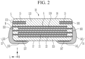
- FIG. 2 is a cross-sectional view taken along line II- II' of FIG. 1 .
- a multilayer ceramic capacitor 10 includes a ceramic body 12, first and second external electrodes 13 and 14, a plurality of first and second internal electrodes 21 and 22, and a dummy electrode 15.
- the ceramic body 12 may be formed by stacking a plurality of dielectric layers 124 in a thickness direction T and then sintering them.
- each of the plurality of adjacent dielectric layers 124 of the ceramic body 12 may be integrated with each other in a state in which the boundaries therebetween are unclear.
- the boundaries between each of the adjacent dielectric layers 124 of the ceramic body 12 may be so integrated that they are difficult to recognize without using a scanning electron microscope (SEM).
- SEM scanning electron microscope
- the ceramic body 12 may have an approximately hexahedral shape with a predetermined size of length, width, and thickness along directions intersecting each other, with the thickness being less than the width, but the present disclosure is not limited thereto.
- the ceramic body 12 may have an approximately rectangular parallelepiped shape, but the portion corresponding to the corner or the vertex may have a rounded shape.
- the surfaces facing each other in the thickness direction T on which the dielectric layers 124 of the ceramic body 12 are stacked are defined as an upper surface 16 and a lower surface 17, the surfaces facing each other in the length direction L of the ceramic body 12 connecting the upper surface and the lower surface are defined as first and second end surfaces 153 and 163, and the surfaces facing each other in the width direction W intersecting vertically to the first and second end surfaces 153 and 163 are defined as first and second side surfaces 19 and 20.
- first and second cover layers 123 and 125 may be disposed outside on both sides of the plurality of first and second internal electrodes 21 and 22 along the thickness direction T of the ceramic body 12, respectively.
- the first cover layer 123 having a predetermined thickness may be provided on an upper portion of the internal electrode at the top, and the second cover layer 125 may be provided on a lower portion of the internal electrode at the bottom.
- the first cover layer 123 and the second cover layer 125 may have the same composition as the dielectric layer 124, and may be formed by stacking one or more dielectric layers that do not include an internal electrode on the upper portion of the internal electrode at the top and the lower portion of the internal electrode at the bottom of the ceramic body 12.
- the first and second cover layers 123 and 125 may serve to prevent damage to the first and second internal electrodes 21 and 22 by physical or chemical stress.
- the dielectric layer 124 may include a high permittivity ceramic material.
- the ceramic material may include a dielectric ceramic including a component such as BaTiOs, CaTiOs, SrTiOs, or CaZrOs, etc.
- auxiliary components such as a Mn compound, an Fe compound, a Cr compound, a Co compound, and a Ni compound may be further included in these components.
- the dielectric layer may be (Ba 1-x Ca x )TiO 3 , Ba (Ti 1-y Ca y )O 3 , (Ba 1-x Ca x ) (Ti 1-y Zr y )O 3 or Ba (Ti 1-y Zr y )O 3 , etc., in which Ca (calcium) and Zr (zirconium) are partially dissolved in BaTiOs, however the present disclosure is not limited thereto.
- the dielectric layer 124 may further include one or more of ceramic additives, organic solvents, plasticizers, binders, and dispersants.
- the ceramic additives may be, for example, a transition metal oxide or carbide, rare earth elements, magnesium (Mg), or aluminum (Al).
- the average thickness of the dielectric layer 111 may be 0.5 ⁇ m to 10 ⁇ m, but the present disclosure is not limited thereto.
- the first and second external electrodes 13 and 14 may be formed by a conductive paste including a conductive metal.
- the first and second external electrodes may be formed by a method of dipping the ceramic body 12 in the conductive paste.
- the conductive metal may include nickel (Ni), copper (Cu), palladium (Pd), gold (Au), or alloys thereof, but the present disclosure is not limited thereto.
- the first and second external electrodes 13 and 14 are disposed at both ends of the ceramic body 12 in the length direction L and respectively include first and second connection portions 133 and 143, and first and second band portions 135 and 145.
- the first connection portion 133 covers a part of the first end surface 153 in the length direction L of the ceramic body 12 and is a part that is electrically connected to the exposed ends of the first or second internal electrode 21 or 22.
- connection portion 143 covers a part of the second end surface 163 in the length direction L of the ceramic body 12, and is a part that is electrically connected to the exposed ends of the first or second internal electrode 21 or 22.
- the first and second band portions 135 and 145 extend from the first and second connection portions 133 and 143, respectively, to cover a portion of the lower surface 17 of the and a portion of the first and second side surfaces 19 and 20 ceramic body 12.
- the first band portion 135 may extend from the first connection portion 133 along the length direction L of the ceramic body 12 and cover a portion of the second cover layer 125.
- the second band portion 145 may extend from the second connection portion 143 in the length direction L of the ceramic body 12 and cover a portion of the second cover layer 125.
- Seed electrode layers 137 and 147 may be printed between the first and second band portions 135 and 145 and the lower surface 17 of the ceramic body 12. That is, the seed electrode layer 137 may be printed between the first band portion 135 and the lower surface 17 of the ceramic body 12, and the seed electrode layer 137 may be printed between the second band portion 145 and the lower surface 17 of the ceramic body 12.
- the seed electrode layers 137 and 147 may be formed by a method of printing a paste including a conductive metal (e.g., nickel (Ni)).
- the seed electrode layers 137 and 147 are regions including a sintering inhibitor in addition to the conductive metal.
- the first connection portion 133 covers a part of the first end surface 153 of the ceramic body 12.
- the first connection portion 133 extends from the bottom to the upward side of the first end surface 153 along the thickness direction T of the ceramic body 12, but does not extend to the top. That is, there is a gap between the top of the first connection portion 133 and the top of the first end surface 153. Accordingly, an upper portion of the first end surface 153 is exposed by the first connection portion 133.
- a portion of the first end surface 153 that is not covered by the first connection portion 133 is referred to as a first exposed surface 173.
- connection portion 143 covers a part of the second end surface 163 of the ceramic body.
- the second connection portion 143 extends from the bottom to the upward side of the second end surface 163 along the thickness direction T of the ceramic body 12, but does not extend to the top. That is, there is a gap between the top of the second connection portion 143 and the top of the second end surface 163. Accordingly, an upper portion of the second end surface 163 is exposed by the second connection portion 143.
- a portion of the second end surface 163 that is not covered by the connection portion 143 is referred to as a second exposed surface 183.
- the first and second exposed surfaces 173 and 183 may be a part of the first cover layer 123. That is, the first and second exposed surfaces 173 and 183 may be parts of both end surfaces of the first cover layer 123 that face each other in the length direction L of the ceramic body 12.
- a dummy electrode 15 is disposed within the first cover layer 123, which includes the first and second exposed surfaces 173 and 183. The dummy electrodes 15 and 15 may be in contact with the first and second exposed surfaces 173 and 183 or project outwardly from the first and second exposed surfaces 173 and 183. The dummy electrode will be discussed in more detail below.
- a plurality of first and second internal electrodes 21 and 22 are alternately stacked with a dielectric layer 124 interposed therebetween.
- the first and second internal electrodes 21 and 22 may be formed and stacked on the ceramic sheet forming the dielectric layer 124, and then alternately arranged in the thickness direction in the ceramic body 12 with one dielectric layer 124 interposed therebetween by sintering.
- These first and second internal electrodes 21 and 22 are electrodes having different polarities, may be disposed facing each other along the stacking direction of the dielectric layer 124, and electrically insulated from each other by the intervening dielectric layer 124.
- the first and second internal electrodes 21 and 22 are disposed to be offset from each other in the length direction with the dielectric layer 124 interposed therebetween, and one ends thereof are exposed through the first and second end surfaces 153 and 163 of the length direction L of the ceramic body 12, respectively.
- the ends of the first and second internal electrodes 21 and 22, which are alternately exposed through first and second end surfaces 153 and 163 of the length direction L of the ceramic body 12 may be electrically connected to the first and second connection portions 133 and 143 of the first and second external electrodes 13 and 14, respectively, on the first and second end surfaces 153 and 163 of the length direction L of the ceramic body 12.
- the first and second internal electrodes 21 and 22 comprise a conductive metal, which may include for example, nickel (Ni) or a nickel (Ni) alloy, but the present disclosure is not limited thereto.
- the capacitance of the multilayer ceramic capacitor 10 is proportional to the overlapping area of the first and second internal electrodes 21 and 22 overlapping each other along the stacking direction of the dielectric layer 124.
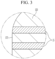
- FIG. 3 is a schematically enlarged cross-sectional view of a region S of FIG. 2 .
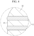
- FIG. 4 is a schematic cross-sectional view of another shape of a region S of FIG. 2 .
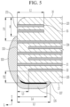
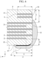
- FIG. 5 is an enlarged view of a part of FIG. 2 .
- FIG. 6 is an enlarged view of another part of FIG. 2 .
- a first cover layer 123 includes a first exposed surface 173 and a second exposed surface 183.
- the first exposed surface 173 is a portion of the first end surface 153 of the ceramic body 12 that is not covered by the first external electrode 13, and the second exposed surface 183 is a portion of the second end surface 163 of the ceramic body 12 that is not covered by the second external electrode 14.
- the first exposed surface 173 as a part of the first end surface 153 is a surface exposed by the first external electrode 13
- the second exposed surface 183 as a part of the second end surface 163 is a surface exposed by the second external electrode 14.
- the second cover layer 125 does not include an exposed surface. That is, both end surfaces of the second cover layer 125 in the length direction L of the ceramic body 12 is covered by the first and second external electrodes 13 and 14.
- both end surfaces of the second cover layer 125 are entirely covered by the first and second external electrodes 13 and 14
- both end surfaces of the first cover layer 123 are partially covered by the first and second external electrodes 13 and 14, and have the exposed surfaces 173 and 183.
- the thickness T1 of the first cover layer 123 may be larger than the thickness T2 of the second cover layer 125.
- the thickness T1 of the first cover layer may be at least twice the thickness T2 of the second cover layer and less than half of the thickness of the ceramic body 12.
- T1 means a distance between the internal electrode closest to the outer surface or an imaginary extension thereof of the first cover layer 123 in the thickness direction T of the ceramic body 12 among the plurality of first and second internal electrodes 21 and 22, and the outer surface or an imaginary extension thereof of the first cover layer 123 in the thickness direction T of the ceramic body 12
- T2 means a distance between the internal electrode closest to the outer surface or an imaginary extension thereof of the second cover layer 125 in the thickness direction T of the ceramic body 12 among the plurality of first and second internal electrodes 21 and 22, and the outer surface or an imaginary extension thereof of the second cover layer 125 in the thickness direction T of the ceramic body 12.
- the first cover layer 123 is covered by the first and second external electrodes 13 and 14 when compared to the second cover layer 125. Therefore, even if an external force of the same magnitude is applied to the first cover layer 123 and the second cover layer 125, the first cover layer 123 may be more likely to break or be damaged, and thus more likely to allow moisture to penetrate. As a result, when the thickness of the first cover layer 123 is the same as the thickness of the second cover layer 125, there is a risk that the moisture resistance reliability of the multilayer ceramic capacitor may be deteriorated.
- the thickness of the first cover layer 123 is formed to be larger than the thickness of the second cover layer 125.
- the moisture permeation path is longer and thus the moisture resistance reliability degradation may be suppressed to a corresponding extent.
- the height H of the exposed surfaces 173 and 183 may be smaller than the thickness T1 of the first cover layer 123.
- H means a distance between the outer surface or an imaginary extension thereof of the first cover layer 123 in the thickness direction T of the ceramic body 12, and the edge of the connection portions 133 and 143 that is on the first cover layer 123 side.
- H means the length of the exposed surfaces 173 and 183 that are not covered by the connection portions 133 and 143 along the thickness direction T of the ceramic body 12.
- T1 means a distance between the internal electrode closest to the outer surface or an imaginary extension thereof of the first cover layer 123 in the thickness direction T of the ceramic body 12 among the plurality of first and second internal electrodes 21 and 22, and the outer surface or an imaginary extension thereof of the first cover layer 123 in the thickness direction T of the ceramic body 12.
- the performance of the multilayer ceramic capacitor may be degraded because the uppermost internal electrode may be drawn out to the exposed surfaces 173 and 183 but not connected to the connection portions 133 and 143 of the external electrodes 13 and 14.
- the multilayer ceramic capacitor 10 includes an active region A and a margin region M.
- the active region A is a region where the plurality of first and second internal electrodes 21 and 22 overlap along the thickness direction T of the ceramic body 12, and the margin region M is a region between the active region A and the two end surfaces 153 and 163 of the ceramic body 12.
- the plurality of first and second internal electrodes 21 and 22 overlap, in the margin region M, the plurality of first internal electrodes 21 or the plurality of second internal electrode 22 are respectively disposed and do not overlap with each other. Therefore, there is a difference in the number of the internal electrodes between the active region A and the margin region M, and there may be a difference in thickness along the thickness direction T of the ceramic body 12 between the active region A and the margin region M accordingly. In other words, there may be a step in the margin region M. The presence of a step reduces the flatness of the ceramic body and prevents the multilayer ceramic capacitor from having an approximately rectangular parallelepiped shape, which may lead to mountability and reliability issues.
- the ceramic body 12 is made of a ceramic material while the external electrodes 13 and 14 are made of a metal (for example, a nickel (Ni)), the difference in the shrinkage rate of the ceramic and the metal during sintering may create a zone of stress concentration in the ceramic body 12, resulting in warpage. If the warpage occurs, when mounting the multilayer ceramic capacitor on the circuit board, a crack may be generated.
- a metal for example, a nickel (Ni)
- the ceramic body 12 according to the present embodiment has a structure in which the thickness is smaller than the width. Since the ceramic body with this structure has a small thickness, there may be a high risk of physical damage such as cracks due to external impact when mounted on the substrate. Furthermore, the lack of flatness of the ceramic body can cause stresses to be concentrated in specific locations during substrate mounting, increasing the likelihood of fracture, resulting in degradation of electrical properties, as well as increasing the likelihood of moisture penetration through the fractured site.
- the occurrence of steps is suppressed to improve flatness, while controlling the difference in shrinkage rate that occurs during the sintering and suppressing the occurrence of warpage.
- the dummy electrodes 15 and 15 are provided in the first cover layer 123 which includes the first and second exposed surfaces 173 and 183.
- the dummy electrodes 15 and 15, like the first and second internal electrodes 21 and 22, may be formed by printing the conductive paste including the conductive metal on the dielectric layer 124.
- the dummy electrodes 15 and 15 may be in contact with the first and second exposed surfaces 173 and 183 or project outwardly from the first and second exposed surfaces 173 and 183.
- the end of the dummy electrode 15 is in contact with the first exposed surface 173, and referring to FIG. 4 , the end of the dummy electrode 15 projects from the first exposed surface 173.
- the dummy electrodes 15 and 15 are arranged to extend inwardly from the first and second exposed surfaces 173 and 183 along the length direction L of the ceramic body 12.
- the length L1 of the dummy electrode 15 may be equal to or smaller than the length L2 of the band portions 135 and 145.
- L1 means the distance between both ends of each of the dummy electrodes 15 and 15 along the length direction L of the ceramic body 12
- L2 means the distance between the end surfaces 153 and 163 or an imaginary extension thereof of the ceramic body 12, and the edge of the band portions 135 and 145 that is opposite the end surfaces 153 and 163 of the ceramic body 12.
- edges of the dummy electrodes 15 and 15 that are opposite the end surfaces 153 and 163 of the ceramic body 12and the edges of the band portions 135 and 145 that are opposite the end surfaces 153 and 163 of the ceramic body 12 may be disposed on the same straight line along the thickness direction T of the ceramic body 12.
- the ceramic body 12 may shrink further toward the dummy electrode 15, which may have a negative effect on preventing the flex crack.
- the length L1 of the dummy electrode 15 may be greater than the length L3 of the margin region.
- L3 means the distance between both ends of the margin region M along the length direction L of the ceramic body 12. If the length L1 of the dummy electrode 15 is smaller than the length L3 of the margin region, it is difficult to reduce the step in the margin region M, which may result in a lower flatness of the ceramic body 12.
- the length L4 of the seed electrode layers 137 and 147 may be greater than the length L3 of the margin region M.
- L4 means the distance between the end surfaces 153 and 163 or an imaginary extension thereof of the ceramic body 12 and the edges of the seed electrode layers 137 and 147 that are opposite the end surfaces 153 and 163 of the ceramic body 12.
- the length L4 of the seed electrode layers 137 and 147 may be equal to or smaller than the length L2 of the band portions 137 and 147.
- the dummy electrodes 15 and 15 may include a plurality of layers, and each layer of the dummy electrodes 15 and 15 may be spaced apart from each other in the thickness direction T of the ceramic body 12. Meanwhile, a plurality of layers of the dummy electrodes 15 and 15 may be disposed at uniform intervals along the thickness direction T of the ceramic body 12.
- the dummy electrodes 15 and 15 may include nickel (Ni), copper (Cu), tin (Sn), palladium (Pd), gold (Au), or alloys thereof, but the present disclosure is not limited thereto.
- the dummy electrodes 15 and 15 may partially overlap with the plurality of first and second internal electrodes 21 and 22 along the thickness direction T of the ceramic body 12.
- disposing the dummy electrodes 15 and 15 in the first cover layer 123 may improve flatness by controlling warping caused by the difference in shrinkage rates of the ceramic and the metal during sintering.
- the flex cracks may be prevented from occurring when the multilayer ceramic capacitor 10 is mounted on the substrate.
- the moisture penetration path can be lengthened, thereby improving moisture resistance reliability.
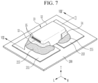
- FIG. 7 is a schematic perspective view showing the multilayer ceramic capacitor shown in FIG. 1 is mounted on a substrate.
- FIG. 8 is a cross-sectional view taken along line VIII-VIII' of FIG. 7 .
- the multilayer ceramic capacitor 10 is connected to the first and second electrode pads 211 and 213 provided on the upper surface of the circuit board 200 through a conductive bonding member 215. That is, the multilayer ceramic capacitor 10 may be mounted on the circuit board 200 through the first and second electrode pads 211 and 213.
- the first and second electrode pads 211 and 213 may be disposed to be spaced apart from each other on the upper surface of the circuit board 200.
- the band portions 135 and 145 of the first and second external electrodes 13 and 14 of the multilayer ceramic capacitor 10 may be secured to the circuit board 200 using the conductive bonding member 215 while disposed to be in contact with the first and second electrode pads 211 and 213.
- the first and connection portions 133 and 143 of the first and second external electrodes 13 and 14 may also be covered with the conductive bonding member 215. Accordingly, the multilayer ceramic capacitor 10 may be electrically connected to the first and second electrode pads 211 and 213 of the circuit board 200.
- the conductive bonding member 215 may include, for example, a solder.
- each of the first and second external electrodes 13 and 14 of the multilayer ceramic capacitor 10 is mounted to the circuit board 200 by being secured to the first and second electrode pads 211 and 213 by the conductive bonding member 215.
- FIG. 9 is a schematic cross-sectional view showing a multilayer ceramic capacitor according to another embodiment.
- the dummy electrodes 15' and 15' extend along the length direction L of the ceramic body 12 within the first cover layer 123, but do not reach the first and second exposed surfaces 173 and 183 of the ceramic body 12. That is, there is a gap between the dummy electrodes 15' and 15' and the first and second exposed surfaces 173 and 183 of the ceramic body 12.
- the multilayer ceramic capacitor according to the embodiment shown in FIG. 9 is the same as the multilayer ceramic capacitor according to the embodiment shown in FIG. 1 , a description of the duplicated or identical portions will be omitted.
Landscapes
- Engineering & Computer Science (AREA)
- Power Engineering (AREA)
- Manufacturing & Machinery (AREA)
- Microelectronics & Electronic Packaging (AREA)
- Chemical & Material Sciences (AREA)
- Ceramic Engineering (AREA)
- Inorganic Chemistry (AREA)
- Ceramic Capacitors (AREA)
- Fixed Capacitors And Capacitor Manufacturing Machines (AREA)
Applications Claiming Priority (1)
| Application Number | Priority Date | Filing Date | Title |
|---|---|---|---|
| KR1020230031803A KR20240138286A (ko) | 2023-03-10 | 2023-03-10 | 적층 세라믹 커패시터 |
Publications (2)
| Publication Number | Publication Date |
|---|---|
| EP4428880A2 true EP4428880A2 (de) | 2024-09-11 |
| EP4428880A3 EP4428880A3 (de) | 2025-03-05 |
Family
ID=90361704
Family Applications (1)
| Application Number | Title | Priority Date | Filing Date |
|---|---|---|---|
| EP24161418.9A Pending EP4428880A3 (de) | 2023-03-10 | 2024-03-05 | Keramischer vielschichtkondensator mit freiliegenden blindelektroden in der oberen dielektrischen deckschicht |
Country Status (5)
| Country | Link |
|---|---|
| US (1) | US20240304386A1 (de) |
| EP (1) | EP4428880A3 (de) |
| JP (1) | JP2024128963A (de) |
| KR (1) | KR20240138286A (de) |
| CN (1) | CN118629782A (de) |
Cited By (1)
| Publication number | Priority date | Publication date | Assignee | Title |
|---|---|---|---|---|
| EP4428883A3 (de) * | 2023-03-10 | 2025-02-26 | Samsung Electro-Mechanics Co., Ltd. | Keramischer mehrschichtkondensator |
Family Cites Families (4)
| Publication number | Priority date | Publication date | Assignee | Title |
|---|---|---|---|---|
| CA900615A (en) * | 1972-05-16 | B. Heron John | High voltage monolithic ceramic capacitor | |
| JP2000106322A (ja) * | 1998-09-29 | 2000-04-11 | Kyocera Corp | 積層セラミックコンデンサ |
| JP2012164966A (ja) * | 2011-01-21 | 2012-08-30 | Murata Mfg Co Ltd | セラミック電子部品 |
| KR102720880B1 (ko) * | 2021-01-15 | 2024-10-23 | 주식회사 아모텍 | 적층형 세라믹 콘덴서 및 이를 구비한 파워 모듈 |
-
2023
- 2023-03-10 KR KR1020230031803A patent/KR20240138286A/ko active Pending
-
2024
- 2024-02-23 US US18/585,603 patent/US20240304386A1/en active Pending
- 2024-03-05 EP EP24161418.9A patent/EP4428880A3/de active Pending
- 2024-03-06 CN CN202410255050.8A patent/CN118629782A/zh active Pending
- 2024-03-07 JP JP2024035050A patent/JP2024128963A/ja active Pending
Cited By (2)
| Publication number | Priority date | Publication date | Assignee | Title |
|---|---|---|---|---|
| EP4428883A3 (de) * | 2023-03-10 | 2025-02-26 | Samsung Electro-Mechanics Co., Ltd. | Keramischer mehrschichtkondensator |
| US12525396B2 (en) | 2023-03-10 | 2026-01-13 | Samsung Electro-Mechanics Co., Ltd. | Multilayer ceramic capacitor |
Also Published As
| Publication number | Publication date |
|---|---|
| CN118629782A (zh) | 2024-09-10 |
| US20240304386A1 (en) | 2024-09-12 |
| EP4428880A3 (de) | 2025-03-05 |
| KR20240138286A (ko) | 2024-09-20 |
| JP2024128963A (ja) | 2024-09-24 |
Similar Documents
| Publication | Publication Date | Title |
|---|---|---|
| US9048026B2 (en) | Multilayered ceramic capacitor, mounting structure of circuit board having multilayered ceramic capacitor mounted thereon, and packing unit for multilayered ceramic capacitor | |
| KR102076150B1 (ko) | 적층 세라믹 커패시터 및 그 실장 기판 | |
| JP2016149555A (ja) | 積層セラミック電子部品及びその実装基板 | |
| KR102436224B1 (ko) | 커패시터 부품 | |
| JP2016149531A (ja) | 積層セラミック電子部品及びその実装基板 | |
| EP4428880A2 (de) | Keramischer vielschichtkondensator mit freiliegenden blindelektroden in der oberen dielektrischen deckschicht | |
| US11862401B2 (en) | Multilayer capacitor and board having the same mounted thereon | |
| EP4443450A2 (de) | Keramischer vielschichtkondensator mit blindelektroden in deckschichten | |
| KR102789010B1 (ko) | 적층형 커패시터 및 그 실장 기판 | |
| US10840019B2 (en) | Electronic component | |
| US12266478B2 (en) | Multilayer electronic component | |
| US20240312717A1 (en) | Multilayer ceramic capacitor | |
| KR102214305B1 (ko) | 적층형 커패시터 | |
| US12525396B2 (en) | Multilayer ceramic capacitor | |
| US20240304390A1 (en) | Multilayer ceramic capacitor | |
| US20230170140A1 (en) | Multilayer electronic component | |
| US20240304382A1 (en) | Electronic component | |
| KR20250029397A (ko) | 적층형 세라믹 전자 부품 | |
| KR20240138444A (ko) | 적층 세라믹 커패시터 |
Legal Events
| Date | Code | Title | Description |
|---|---|---|---|
| PUAI | Public reference made under article 153(3) epc to a published international application that has entered the european phase |
Free format text: ORIGINAL CODE: 0009012 |
|
| STAA | Information on the status of an ep patent application or granted ep patent |
Free format text: STATUS: THE APPLICATION HAS BEEN PUBLISHED |
|
| AK | Designated contracting states |
Kind code of ref document: A2 Designated state(s): AL AT BE BG CH CY CZ DE DK EE ES FI FR GB GR HR HU IE IS IT LI LT LU LV MC ME MK MT NL NO PL PT RO RS SE SI SK SM TR |
|
| PUAL | Search report despatched |
Free format text: ORIGINAL CODE: 0009013 |
|
| AK | Designated contracting states |
Kind code of ref document: A3 Designated state(s): AL AT BE BG CH CY CZ DE DK EE ES FI FR GB GR HR HU IE IS IT LI LT LU LV MC ME MK MT NL NO PL PT RO RS SE SI SK SM TR |
|
| RIC1 | Information provided on ipc code assigned before grant |
Ipc: H01G 4/30 20060101ALI20250128BHEP Ipc: H01G 4/232 20060101ALI20250128BHEP Ipc: H01G 2/06 20060101ALI20250128BHEP Ipc: H01G 4/012 20060101AFI20250128BHEP |
|
| STAA | Information on the status of an ep patent application or granted ep patent |
Free format text: STATUS: REQUEST FOR EXAMINATION WAS MADE |
|
| 17P | Request for examination filed |
Effective date: 20250701 |