EP4426084A1 - Anzeigevorrichtung und anzeigetafel und herstellungsverfahren dafür - Google Patents
Anzeigevorrichtung und anzeigetafel und herstellungsverfahren dafür Download PDFInfo
- Publication number
- EP4426084A1 EP4426084A1 EP22938825.1A EP22938825A EP4426084A1 EP 4426084 A1 EP4426084 A1 EP 4426084A1 EP 22938825 A EP22938825 A EP 22938825A EP 4426084 A1 EP4426084 A1 EP 4426084A1
- Authority
- EP
- European Patent Office
- Prior art keywords
- light
- layer
- display area
- display panel
- driving backplane
- Prior art date
- Legal status (The legal status is an assumption and is not a legal conclusion. Google has not performed a legal analysis and makes no representation as to the accuracy of the status listed.)
- Pending
Links
Images


Classifications
-
- H—ELECTRICITY
- H10—SEMICONDUCTOR DEVICES; ELECTRIC SOLID-STATE DEVICES NOT OTHERWISE PROVIDED FOR
- H10K—ORGANIC ELECTRIC SOLID-STATE DEVICES
- H10K59/00—Integrated devices, or assemblies of multiple devices, comprising at least one organic light-emitting element covered by group H10K50/00
- H10K59/80—Constructional details
- H10K59/875—Arrangements for extracting light from the devices
- H10K59/879—Arrangements for extracting light from the devices comprising refractive means, e.g. lenses
-
- G—PHYSICS
- G06—COMPUTING OR CALCULATING; COUNTING
- G06F—ELECTRIC DIGITAL DATA PROCESSING
- G06F3/00—Input arrangements for transferring data to be processed into a form capable of being handled by the computer; Output arrangements for transferring data from processing unit to output unit, e.g. interface arrangements
- G06F3/01—Input arrangements or combined input and output arrangements for interaction between user and computer
- G06F3/03—Arrangements for converting the position or the displacement of a member into a coded form
- G06F3/041—Digitisers, e.g. for touch screens or touch pads, characterised by the transducing means
- G06F3/0412—Digitisers structurally integrated in a display
-
- H—ELECTRICITY
- H10—SEMICONDUCTOR DEVICES; ELECTRIC SOLID-STATE DEVICES NOT OTHERWISE PROVIDED FOR
- H10K—ORGANIC ELECTRIC SOLID-STATE DEVICES
- H10K59/00—Integrated devices, or assemblies of multiple devices, comprising at least one organic light-emitting element covered by group H10K50/00
- H10K59/10—OLED displays
- H10K59/12—Active-matrix OLED [AMOLED] displays
- H10K59/122—Pixel-defining structures or layers, e.g. banks
-
- H—ELECTRICITY
- H10—SEMICONDUCTOR DEVICES; ELECTRIC SOLID-STATE DEVICES NOT OTHERWISE PROVIDED FOR
- H10K—ORGANIC ELECTRIC SOLID-STATE DEVICES
- H10K59/00—Integrated devices, or assemblies of multiple devices, comprising at least one organic light-emitting element covered by group H10K50/00
- H10K59/30—Devices specially adapted for multicolour light emission
- H10K59/38—Devices specially adapted for multicolour light emission comprising colour filters or colour changing media [CCM]
-
- H—ELECTRICITY
- H10—SEMICONDUCTOR DEVICES; ELECTRIC SOLID-STATE DEVICES NOT OTHERWISE PROVIDED FOR
- H10K—ORGANIC ELECTRIC SOLID-STATE DEVICES
- H10K59/00—Integrated devices, or assemblies of multiple devices, comprising at least one organic light-emitting element covered by group H10K50/00
- H10K59/40—OLEDs integrated with touch screens
-
- H—ELECTRICITY
- H10—SEMICONDUCTOR DEVICES; ELECTRIC SOLID-STATE DEVICES NOT OTHERWISE PROVIDED FOR
- H10K—ORGANIC ELECTRIC SOLID-STATE DEVICES
- H10K59/00—Integrated devices, or assemblies of multiple devices, comprising at least one organic light-emitting element covered by group H10K50/00
- H10K59/80—Constructional details
- H10K59/8791—Arrangements for improving contrast, e.g. preventing reflection of ambient light
- H10K59/8792—Arrangements for improving contrast, e.g. preventing reflection of ambient light comprising light absorbing layers, e.g. black layers
-
- G—PHYSICS
- G06—COMPUTING OR CALCULATING; COUNTING
- G06F—ELECTRIC DIGITAL DATA PROCESSING
- G06F2203/00—Indexing scheme relating to G06F3/00 - G06F3/048
- G06F2203/041—Indexing scheme relating to G06F3/041 - G06F3/045
- G06F2203/04111—Cross over in capacitive digitiser, i.e. details of structures for connecting electrodes of the sensing pattern where the connections cross each other, e.g. bridge structures comprising an insulating layer, or vias through substrate
-
- G—PHYSICS
- G06—COMPUTING OR CALCULATING; COUNTING
- G06F—ELECTRIC DIGITAL DATA PROCESSING
- G06F2203/00—Indexing scheme relating to G06F3/00 - G06F3/048
- G06F2203/041—Indexing scheme relating to G06F3/041 - G06F3/045
- G06F2203/04112—Electrode mesh in capacitive digitiser: electrode for touch sensing is formed of a mesh of very fine, normally metallic, interconnected lines that are almost invisible to see. This provides a quite large but transparent electrode surface, without need for ITO or similar transparent conductive material
-
- G—PHYSICS
- G06—COMPUTING OR CALCULATING; COUNTING
- G06F—ELECTRIC DIGITAL DATA PROCESSING
- G06F3/00—Input arrangements for transferring data to be processed into a form capable of being handled by the computer; Output arrangements for transferring data from processing unit to output unit, e.g. interface arrangements
- G06F3/01—Input arrangements or combined input and output arrangements for interaction between user and computer
- G06F3/03—Arrangements for converting the position or the displacement of a member into a coded form
- G06F3/041—Digitisers, e.g. for touch screens or touch pads, characterised by the transducing means
- G06F3/044—Digitisers, e.g. for touch screens or touch pads, characterised by the transducing means by capacitive means
- G06F3/0446—Digitisers, e.g. for touch screens or touch pads, characterised by the transducing means by capacitive means using a grid-like structure of electrodes in at least two directions, e.g. using row and column electrodes
Definitions
- the present disclosure relates to the display technical field, and in particular, to a display device, a display panel and a method for manufacturing the display panel.
- a display panel is an indispensable part of an electronic device, such as mobile phone, or computer.
- Display panels include liquid crystal display panels, organic electroluminescent display panels, and the like. At present, people have increasingly high requirements for display effects, but the brightness of existing display panels still needs to be improved, and display abnormalities such as color shift are prone to occur.
- the present disclosure provides a display device, a display panel and a method for manufacturing the display panel.
- a display panel including:
- the display panel further includes: a filter layer covering the lens layer and including a plurality of filter units distributed in an array, wherein any one of at least a part of the lenses is covered by one of the filter units, each of the filter units only allows monochromatic light to pass through, and colors of monochromatic light passing through at least two of the filter units are different, and a refractive index of the filter layer is smaller than a refractive index of a lens which is covered by the filter layer.
- the refractive index of the organic layer is the same as the refractive index of the filter layer.
- At least a part of the lenses only allow monochromatic light to pass through, and colors of monochromatic light passing through at least two of the lenses are different, and the refractive index of the organic layer is smaller than the refractive index of the lenses.
- the refractive index of the lens is the same as the refractive index of the first inorganic layer.
- the first inorganic layer is recessed at the openings to form recesses, and each of the lenses includes a filling portion filling one of the recesses and a protrusion portion protruding from the one of the recesses.
- the protrusion portion has a top surface and an outer peripheral surface surrounding the top surface, and the outer peripheral surface is connected between the top surface and the filling portion; wherein in one of the lenses and a recess which the one of the lenses fills, an orthographic projection of an opening corresponding to the recess on the driving backplane is located within an orthographic projection of the top surface on the driving backplane, the outer periphery surface shrinks in a direction away from the driving backplane, and an orthographic projection of the outer peripheral surface on the driving backplane surrounds outside of the orthographic projection of the opening corresponding to the recess on the driving backplane.
- the outer peripheral surface is formed by a plurality of surrounding planes, and each of the planes is an inclined slope, and a slope angle of each of the planes is not greater than 90°.
- the display panel further includes: a light-absorbing layer arranged on a same side of the driving backplane as the light-emitting devices, wherein an orthographic projection of the light-absorbing layer on the driving backplane separates orthographic projections of the lenses on the driving backplane.
- the display panel includes a display area and a peripheral area located outside the display area, the display area has a sub-display area and a main display area located outside the sub-display area, the light-emitting devices are distributed in the main display area and the sub-display area, and the light-absorbing layer is located in the main display area.
- the display panel includes a display area and a peripheral area located outside the display area, the display area has a sub-display area and a main display area located outside the sub-display area, and the light-emitting devices are distributed in the main display area and the sub-display area; wherein the display panel further includes: the light-absorbing layer arranged in the main display area and the sub-display area, wherein the light-absorbing layer is provided with a plurality of light transmission holes located in the sub-display area.
- the display panel further includes:
- At least a part of the pixel definition layer is made of a light-absorbing material.
- the display panel includes a display area and a peripheral area located outside the display area, the display area has a sub-display area and a main display area located outside the sub-display area, and the light-emitting devices are distributed in the main display area and the sub-display area; wherein the pixel definition layer in the sub-display area is made of a light-transmitting material, and the pixel definition layer in the main display area is made of the light-absorbing material.
- the display panel includes a display area and a peripheral area located outside the display area, the display area has a sub-display area and a main display area located outside the sub-display area, and the light-emitting devices are distributed in the main display area and the sub-display area; wherein the pixel definition layer is made of the light-absorbing material, and the pixel definition layer in the sub- display area is provided with a light-transmitting hole.
- the display panel further includes:
- a method for manufacturing a display panel including:
- a display device including the display panel according to any one of the above embodiments.
- Example implementations will now be described more fully with reference to the accompanying drawings.
- Example implementations can, however, be embodied in many forms and should not be construed as limited to the implementations set forth herein; rather, these implementations are provided so that the present disclosure will be thorough and complete, and will fully convey the concept of example implementations to those skilled in the art.
- the same reference numerals in the drawings denote the same or similar structures, and thus their detailed descriptions will be omitted.
- the drawings are merely schematic illustrations of the present disclosure and are not necessarily drawn to scale.
- a row direction X and a column direction Y herein are only two directions perpendicular to each other.
- the row direction X may be horizontal
- the column direction Y may be vertical, but the present disclosure is not limited thereto. If rotation of a display panel occurs, the actual orientation of the row direction X and the column direction Y may change.
- the X direction in the drawings exemplarily shows the row direction
- the Y direction exemplarily shows the column direction.
- a display panel may include a driving backplane and multiple light-emitting devices located on one side of the driving backplane.
- Each light-emitting device may be an organic light-emitting diode (OLED).
- Image display may be realized by controlling the light-emitting devices to emit light independently by the driving backplane.
- the display panel further includes an encapsulation layer, which may cover the light-emitting devices and play a protective role of blocking external water and oxygen.
- the encapsulation layer may include a first inorganic layer, an organic layer and a second inorganic layer.
- the first inorganic layer covers the light-emitting devices
- the organic layer is arranged on a surface of the first inorganic layer away from the driving backplane
- the second inorganic layer covers the organic layer.
- the light emitted by the light-emitting devices needs to pass through the first inorganic layer, the organic layer and the second inorganic layer when it is emitted.
- the inventor found that since the refractive index of the organic layer is lower than that of the first inorganic layer, part of the light emitted by the light-emitting devices will be totally reflected at the interface between the first inorganic layer and the organic layer, and thus it is difficult to improve the light extraction efficiency.
- To increase the brightness of the display panel it is necessary to increase the power of the light-emitting devices, and this will result in an increase in the power consumption of the display panel.
- the inventor further found that since the distance between the interface and the light-emitting devices is only the thickness of the first inorganic layer, the distance is relatively short and the interface is roughly flat, when the light totally reflected by the interface is reflected by first electrode(s) of the light-emitting devices and reaches the interface again, the incident angle does not change significantly and the total reflection angle may still be reached, and thus the total reflection will occur again. This results in that the light which is totally reflected will experience back-and-forth reflections between the light-emitting devices and the interface between the first inorganic layer and the organic layer, and light never gets out, and thus it is difficult to improve the light extraction efficiency of the display panel.
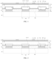
- the display panel may include a driving backplane BP, a light-emitting layer OL, a first inorganic layer CVD1, a lens layer LL, an organic layer IJP and a second inorganic layer CVD2.
- the light-emitting layer OL is arranged on a side of the driving backplane BP and includes a pixel definition layer PDL and a plurality of light-emitting devices LD.
- the pixel definition layer PDL has a plurality of openings PH, and one of the light-emitting devices LD is defined in one of the openings PH.
- the first inorganic layer CVD1 covers the light-emitting layer OL.
- the lens layer LL is arranged on a surface of the first inorganic layer CVD1 away from the driving backplane BP, and includes a plurality of lenses. One of the lenses and one of the light-emitting devices LD are arranged correspondingly.
- the organic layer IJP covers the lens layer LL and the first inorganic layer CVD1.
- a refractive index of the organic layer IJP is smaller than a refractive index of the first inorganic layer CVD1 and smaller than a refractive index of the lenses.
- the second inorganic layer CVD2 covers the organic layer IJP.
- the refractive index of the lenses is greater than or equal to the refractive index of the first inorganic layer CVD1
- the light emitted by the light-emitting devices LD will not be totally reflected at the interface where the first inorganic layer CVD1 contacts the lenses, and thus the light may enter the lenses through the first inorganic layer CVD1.
- each lens is a three-dimensional structure, its surface is no longer a simple plane (the interface where the first inorganic layer CVD1 contacts the organic layer IJP), the total reflection angles of different areas may be different, and at least part of light which experiences back-and-forth reflections between the surface of the lens and a light-emitting device LD and cannot get out may be reduced.
- the light extraction efficiency may be increased, and it is beneficial to reduce power consumption while ensuring the brightness.
- the difference between the refractive index of the first inorganic layer CVD1 and the refractive index of the lenses may be smaller than the difference between the refractive index of the lenses and the refractive index of the first inorganic layer CVD1, even if total reflection occurs at the interface between the lenses and the first inorganic layer CVD1, the influence of the total reflection may also be reduced as compared with a case where the organic layer IJP is directly in contact with the first inorganic layer CVD1, thereby improving the light extraction efficiency.
- the first inorganic layer CVD1, the organic layer IJP and the second inorganic layer CVD2 may form a thin-film encapsulation structure to prevent external water and oxygen from corroding the light-emitting devices LD.
- the lens layer LL is integrated inside the thin film encapsulation structure, which can prevent the display panel from being too thick while improving the light extraction efficiency.
- the following provides an exemplary description of the basic structure of the display panel of the present disclosure.
- the driving backplane BP has a driving circuit, which may drive the light-emitting devices LD to emit light to display images.
- the driving backplane BP may include a substrate and a circuit layer on a side of the substrate.
- the substrate may be a flat plate structure, and its material may be a hard material such as glass, or a soft material such as polyimide.
- the circuit layer may be arranged on a side of the substrate, and the circuit layer may include a driving circuit, which may drive the light-emitting devices LD to emit light.
- the display panel may be at least divided into a display area AA and a peripheral area SA located outside the display area AA.
- an area of the circuit layer located in the display area AA is a pixel area
- an area located in the peripheral area SA is an edge area, that is, the edge area is located outside the pixel area.
- the driving circuit may include at least one pixel circuit located in the pixel area and at least one peripheral circuit located in the edge area.
- the pixel circuit may be a pixel circuit such as 3T1C, 6T1C, 7T1C, or 7T2C, as long as it may drive a light-emitting device LD to emit light, and its structure is not particularly limited here.
- the number of at least one pixel circuit may be the same as the number of light-emitting devices LD, and they are connected to light-emitting devices LD in a one-to-one correspondence, so as to respectively control a corresponding light-emitting device LD to emit light.
- the nTmC indicates that a pixel circuit includes n transistors (indicated by the letter "T") and m capacitors (indicated by the letter "C").
- the same pixel circuit may also be connected with multiple light-emitting devices LD, and simultaneously drive the multiple light-emitting devices LD to emit light, which is not specifically limited here.
- the at least one peripheral circuit is connected with the pixel circuit(s), and is used for inputting a driving signal to the pixel circuit(s) so as to control the light-emitting devices LD to emit light.
- the at least one peripheral circuit may include a gate driving circuit and a light-emitting control circuit.
- the at least one peripheral circuit may also include other circuits, and the specific structure of the at least one peripheral circuit is not specifically limited here.
- the above-mentioned circuit layer may include a plurality of thin film transistors and capacitors.
- the thin film transistors may be top-gate or bottom-gate thin film transistors.
- Each thin film transistor may include an active layer and a gate.
- the circuit layer may include a semiconductor layer, a first gate insulating layer, a first gate layer, a second gate insulating layer, a second gate layer, an interlayer dielectric layer, a first source and drain layer, a passivation layer, a first planarization layer, a second source and drain layer and a second planarization layer which are sequentially stacked in a direction away from the substrate.
- the specific patterns of the film layers may be determined depending on specific composition of the driving circuits, which is not specifically limited here.
- the light-emitting layer OL is arranged on a side of the driving backplane BP, and includes light-emitting devices LD and a pixel definition layer PDL for limiting the range of each light-emitting device LD.
- the pixel definition layer PDL and the light-emitting devices LD may be arranged on a surface of the second planarization layer away from the substrate.
- the orthographic projection of each light-emitting device LD on the circuit layer may be located in the pixel area, that is, in the display area AA of the display panel.
- Each light-emitting device LD may include a first electrode ANO, a second electrode CAT, and a light-emitting material layer EL between the first electrode ANO and the second electrode CAT. By applying electric signal(s) to the first electrode ANO and the second electrode CAT, the light-emitting material layer EL may be excited to emit light.
- the light-emitting device LD may be an organic light-emitting diode (OLED).
- the first electrodes ANOs of light-emitting devices LD are distributed as being spaced from each other, and the pixel definition layer PDL is provided with openings PH exposing each of first electrodes ANO. That is, one opening PH exposes one first electrode ANO.
- the pixel definition layer PDL may be used to define the range of each light-emitting device LD, the range of an opening PH is the range of a light-emitting device LD, and the boundary of the orthographic projection of the light-emitting device LD on the driving backplane BP is the boundary of the opening PH on the driving backplane BP.
- the orthographic projection of the light-emitting device LD on the driving backplane BP is the outer boundary of the orthographic projection of the opening PH on the driving backplane BP.
- the shape of the opening PH that is, the shape of the boundary of its orthographic projection on the driving backplane BP, may be a polygon such as a rectangle, a pentagon, or a hexagon, or an ellipse, a sector, or other shapes.
- the shape of the opening PH is not specially limited.
- the light-emitting material layer EL is at least partly located in the opening PH and stacked with the first electrode ANO.
- the light-emitting material layer EL may include a hole injection layer, a hole transport layer, a light-emitting material layer EL, an electron transport layer, and an electron injection layer sequentially stacked in a direction away from the driving backplane BP.
- other structures may also be used, as long as they may cooperate with the first electrode ANO and the second electrode CAT to emit light.
- the second electrode CAT may cover the light-emitting material layer EL, and the second electrode CAT may be a continuous whole layer structure, so that light-emitting devices LD may share the same second electrode CAT.
- the second electrode CAT may be recessed into openings PH at positions corresponding to the openings PH.
- the second electrode CAT may be the cathodes of the light-emitting devices LD, which may adopt a light-transmitting structure, so that the light-emitting devices LD may emit light in a direction away from the driving backplane BP.
- the material of the second electrode CAT may be metal magnesium, silver or its alloys, etc., and under a certain thickness, the second electrode may transmit light while conducting electricity.
- the first electrode(s) ANO may be in an opaque structure, so that the light-emitting devices LD have a top emission structure.
- the second electrode CAT may extend to the edge area of the circuit layer, and is connected with a common power signal line, and may receive a common power signal.
- the common power signal line may be arranged in the same layer as the first electrodes ANO, and thus the second electrode CAT may be in the edge area and connected to the common power signal line.
- a pixel power signal may be applied to a first electrode ANO through the control of a pixel circuit, and the pixel circuit may receive the pixel power signal through a pixel power line located in the second source and drain layer, and apply the common power signal to the second electrode DAT through the common power signal line to excite the light-emitting layer OL to emit light.
- the specific principle of organic electroluminescence will not be described in detail here.
- each light-emitting device LD may emit light independently, and the color of light emitted by different light-emitting devices LD may be different.
- the light-emitting material layer EL may include multiple light-emitting units arranged as being spaced in respective openings PH in a one-to-one correspondence. Each light-emitting unit may emit light independently, and the color of light emitted by each light-emitting unit may be different, so that color display may be directly realized.
- the second electrode CAT covers the light-emitting material layer EL, and also covers an area of the pixel definition layer PDL not covered by the light-emitting material layer EL.
- the light-emitting material layer EL may also cover the pixel definition layer PDL and each first electrode ANO at the same time, that is, light-emitting devices LD may share the same light-emitting material layer EL. Also, light-emitting devices LD emit the same color. In order to realize color display, a filter structure that only transmits monochromatic light may be provided on a side of the light-emitting devices LD away from the driving backplane BP.
- the display panel may also include an encapsulation layer TFE, which may cover respective light-emitting devices LD, and is used to protect the light-emitting layer OL, and prevent external water and oxygen from corroding the light-emitting devices LD.
- the encapsulation layer TFE may adopt a method of thin film encapsulation, which may include the first inorganic layer CVD1, the organic layer IJP and the second inorganic layer CVD2.
- the first inorganic layer CVD1 may cover respective light-emitting devices LD, that is, the first inorganic layer CVD1 may cover a surface of the second electrode CAT away from the driving backplane BP.
- the material of the first inorganic layer CVD1 may include an inorganic insulating material such as silicon nitride or silicon oxide. Also, since the second electrode CAT is recessed at the positions corresponding to the openings PH, correspondingly, the first inorganic layer CVD1 is also recessed at the positions corresponding to the openings PH, forming recesses SP.
- the organic layer IJP may be arranged on a surface of the first inorganic layer CVD1 away from the driving backplane BP, and the boundary of the organic layer IJP may be defined as being in an inner side of the boundary of the first inorganic layer CVD1 by a blocking dam in the peripheral area SA, and the boundary of the orthographic projection of the organic layer IJP on the driving backplane BP may be located in the peripheral area SA, ensuring that the organic layer IJP can cover each light-emitting device LD.
- the material of the organic layer IJP may be an organic material such as resin, whose refractive index is smaller than the refractive index of the first inorganic layer CVD1, and smaller than the refractive index of the second inorganic layer CVD2, and the difference between the two may be 0.5.
- the refractive index of the first inorganic layer CVD 1 may be 1.6-1.8
- the refractive index of the organic layer IJP may be 1.1-1.3; of course, other values may also be used.
- the second inorganic layer CVD2 may cover the organic layer IJP and the first inorganic layer CVD1 that is not covered by the organic layer IJP.
- the second inorganic layer CVD2 may block the intrusion of water and oxygen, and planarization may be realized through the flexible organic layer IJP.
- the material of the second inorganic layer CVD2 may include an inorganic insulating material such as silicon nitride, or silicon oxide. It should be noted that the color filter layer mentioned in some implementations above may be arranged on a side of the encapsulation layer TFE away from the driving backplane BP.
- the display panel may further include a touch layer TPS, which may be arranged on a side of the encapsulation layer TFE away from the driving backplane BP, and used for sensing a touch operation.
- a touch layer TPS adopting a mutual capacitive touch structure as an example, as shown in FIG. 4 and FIG. 5 , the touch layer TPS may include a plurality of first touch electrodes Tx and a plurality of second touch electrodes Rx.
- the first touch electrodes Tx may be distributed as being spaced from each other along the row direction X.
- One of the first touch electrodes Tx may include a plurality of first electrode blocks Txc distributed as being spaced from each other along the column direction Y and interconnect bridges BR each of which is used for connecting two adjacent first electrode blocks Txc.
- the second touch electrodes Rx may be distributed as being spaced from each other along the column direction Y
- One of the second touch electrodes Rx includes a plurality of second electrode blocks Rxc connected in series along the row direction X.
- One of the interconnect bridges BR and a second touch electrode Rx cross and are insulated.
- One of a first touch electrodes Tx and a second touch electrodes Rx may be used as a transmitting electrode, and the other may be used as a receiving electrode, both of which are connected to a peripheral touch driving circuit.
- the above-mentioned first electrode blocks Txc and second touch electrodes Rx are located in the touch electrode layer TMB, that is, the first electrode blocks Txc and the second touch electrodes Rx are arranged in the same layer, and thus they may be formed simultaneously through the same process.
- the interconnect bridges BR may be located in an interconnect layer, which may be located between the touch electrode layer TMB and the encapsulation layer TFE.
- the touch layer TPS may also include a buffer layer TLD and an isolation layer SEP.
- the buffer layer TLD may be arranged on a surface of the encapsulation layer TFE away from the driving backplane BP, and its material may be silicon nitride, silicon oxide or other insulating materials, which are not specifically limited here.
- the interconnect layer may be arranged on a surface of the buffer layer TLD away from the driving backplane BP, and includes a plurality of interconnect bridges BR.
- the interconnect layer may be made of metal or other conductive materials.
- the isolation layer SEP may cover the interconnect layer, and the material of the isolation layer SEP may be an insulating material such as silicon nitride, or silicon oxide, which are not specifically limited here.
- the touch electrode layer TMB may be arranged on the surface of the isolation layer SEP away from the driving backplane BP, and includes the first electrode blocks Txc and the second touch electrodes Rx mentioned above.
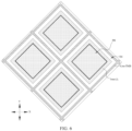
- the touch layer TPS may also use a self-capacitive touch structure.
- the touch layer TPS may include a touch electrode layer TMB, and the touch electrode layer TMB may include a plurality of electrode blocks distributed in an array, and each electrode block may be connected to a peripheral touch driving circuit through an independent trace.
- the specific structure of the self-capacitive touch structure is not limited here, as long as the touch control function may be realized.
- the touch electrode layer TMB may be a mesh structure formed by a plurality of connected channel lines Ltm, and the mesh structure has a plurality of holes TH.
- one light-emitting device LD may correspond to one hole TH, that is, the orthographic projection of one light-emitting device LD on the driving backplane BP is located within the orthographic projection of the one hole TH on the driving backplane BP.
- One hole TH may correspond to only one light-emitting device LD, and the shape of the hole TH may be the same as that of the light-emitting device LD. Certainly, in other implementations of the present disclosure, one hole TH may correspond to a plurality of light-emitting devices LD.
- the touch layer TPS may further include a protective layer TOC, which may cover the touch electrode layer TMB.
- the touch electrode layer TMB may be protected by the protective layer TOC, and planarization may be realized, so as to form a film layer on top of the touch layer TPS.
- the display panel may further include a cover plate, which may be made of a transparent material such as glass or acrylic, and may be provided on a side of the touch layer TPS away from the driving backplane BP.
- the cover plate may be provided on a side of the protective layer TOC away from the driving backplane BP.
- the film layer covered by the cover plate may be protected by the cover plate.
- the following describes the lens layer LL in detail based on the above display panel architecture.
- the lens layer LL may be arranged in the encapsulation layer TFE to avoid increasing the thickness of the display panel.
- the lens layer LL may be arranged on a surface of the first inorganic layer CVD1 away from the driving backplane BP, and covered by the organic layer IJP, so that the lens layer LL is placed in the encapsulation layer TFE.
- the lens layer LL may include a plurality of lenses distributed in an array. In the direction perpendicular to the driving backplane BP, at least a part of the light-emitting devices LD may be arranged corresponding to the lenses, and one lens may be arranged corresponding to one light-emitting device LD, that is, one lens is arranged as corresponding to an opening PH.
- the corresponding arrangement of a lens and a light-emitting device LD means that the orthographic projections of the lens and the light-emitting device LD on the driving backplane BP at least partially overlap.
- the number of lenses may be the same as the number of light-emitting devices LD, and each lens may be set corresponding to a light-emitting device LD, so that at least part of the light emitted by each light-emitting device LD may pass through its corresponding lens.
- the refractive index of the lens may be not less than the refractive index of the first inorganic layer CVD1.
- the refractive index of the lens is equal to the refractive index of the first inorganic layer CVD1. Since the lens is bonded to the first inorganic layer CVD1, when the light propagates from the first inorganic layer CVD1 to the lens, the light path does not change.
- the refractive index of the lens may also be greater than that of the first inorganic layer CVD1, as long as total reflection can be avoided.
- the condition of total reflection at the interface where the first inorganic layer CVD1 contacts the organic layer IJP in the related art is destroyed, preventing total reflection from occurring at the interface, thereby achieving light extraction.
- the lens is a three-dimensional structure, its surface is no longer a pure plane (the interface where the first inorganic layer CVD1 contacts the organic layer IJP), the total reflection angles of different areas may be different, the light which experiences back-and-forth reflections between the surface of the lens and the light-emitting device LD and cannot get out is reduced, thereby improving the light extraction efficiency.
- the refractive index of the lens may be smaller than the refractive index of the first inorganic layer CVD1, but the refractive index of the lens is greater than the refractive index of the organic layer IJP, so that the difference between the refractive index of the first inorganic layer CVD1 and the refractive index of the lens is smaller than the difference between the refractive index of the first inorganic layer CVD1 and the refractive index of the organic layer IJP.
- the difference between the refractive index of the first inorganic layer CVD1 and the refractive index of the lens is less than 0.5, and the difference between the refractive index of the first inorganic layer CVD1 and the organic layer IJP may be 0.5.
- the present disclosure can reduce the light totally reflected at the surface of the first inorganic layer CVD1 away from the driving backplane BP, thereby improving the light extraction efficiency.
- the boundary of the lens may surround outside of the opening PH. That is, the range covered by the lens is not smaller than the range of the light-emitting device LD, so that all the light emitted by the light-emitting device LD can enter the lens, without being totally reflected caused by not being covered by the lens.
- the shape of the boundary of the orthographic projection of the lens on the driving backplane BP may be the same as the shape of the boundary of the orthographic projection of the opening PH on the driving backplane BP.
- the shape of the opening PH is polygon such as rectangle, rhombus, pentagon or hexagon, and the boundary of the orthographic projection of the lens on the driving backplane BP is also the same polygon; if the shape of the opening PH is elliptical, the boundary of the orthographic projection of the lens on the driving backplane BP is also elliptical.
- the shape of the opening PH is polygon such as rectangle, rhombus, pentagon or hexagon
- the boundary of the orthographic projection of the lens on the driving backplane BP is also the same polygon; if the shape of the opening PH is elliptical, the boundary of the orthographic projection of the lens on the driving backplane BP is also elliptical.
- the shape of the boundary of the orthographic projection of the opening PH on the driving backplane BP is a polygon
- the shape of the boundary of the orthographic projection of the lens on the driving backplane BP is the same polygon
- the sides of the polygon of the orthographic projection of the lens are parallel to or coincide with the sides of the polygon of the orthographic projection of the opening PH in a one-to-one correspondence.
- a lens may include a filling portion Lf and a protrusion portion Lb.
- the filling portion Lf may fill the recess SP, and its shape is the same as that of the recess SP.
- the protrusion portion Lb is stacked on a side of the filling portion Lf away from the driving backplane BP, and protrudes from the recess SP, that is, the protrusion portion Lb is located above the surface of the first inorganic layer CVD1 away from the driving backplane BP, and the filling portion Lf is located below the surface.
- the protrusion portion Lb has a top surface Lbt and an outer peripheral surface Lbs surrounding the top surface Lbt, and the outer peripheral surface Lbs is connected between the top surface Lbt and the filling portion Lf.
- the top surface Lbt is the surface of the lens away from the driving backplane BP, and the top surface Lbt may be a plane parallel to the driving backplane BP, or may be an arc or other curved surface.
- the outer peripheral surface Lbs extends around the edge of the top surface Lbt.
- the orthographic projection of the opening PH corresponding to the recess SP on the driving backplane BP is located within the orthographic projection of the top surface Lbt on the driving backplane BP, that is, the top surface Lbt is not smaller than the opening PH.
- the present disclosure may also achieve color display or reduce the reflection of ambient light for different implementations through light filtering.
- the following is an exemplary description.
- a lens is a transparent structure that may transmit white light.
- a filter layer CF is formed in the encapsulation layer TFE.
- the filter layer may include a plurality of filter units CFU that only allow monochromatic light to pass through.
- the number of filter units CFU may be less than or equal to the number of lenses and distributed in an array.
- Each filter unit CFU may cover a lens, and the organic layer IJP covers each filter unit CFU. Also, the color of the monochromatic light allowed to pass though by different filter units CFU may be different.
- the filter units CFU include a filter unit CFU that may all red light to pass through, a filter unit CFU that may allow green light to pass through, and a filter unit CFU that may allow blue light to pass through.
- the material of the filter layer CF may be an organic material such as resin, as long as the material can achieve light filtering. Color display may be realized or the effect of reducing the reflection of ambient light may be realized through the filter function of the filter units CFUs.
- the light-emitting material layer EL may include a plurality of spaced light-emitting units arranged in openings PH in a one-to-one correspondence. Each light-emitting unit may emit light independently, and the color of emitted light may be different. Correspondingly, the color of light emitted by different light-emitting devices LD may be different. In this implementation, at least three kinds of light-emitting devices LD with different color of emitted light are included, for example, light-emitting devices LD that emit red light, light-emitting devices LD that emit green light, and light-emitting devices LD that emit blue light.
- the color of the monochromatic light that a filter unit CFU allows to pass through is the same as the color of light emitted by the light-emitting device LD corresponding to the covered lens, so that the light emitted by the light-emitting device LD may pass through the corresponding filter unit CFU, and the color of the light emitted by the light-emitting device LD is the same as the color of the corresponding filter unit CFU.
- the realization of color display does not necessarily depend on the filtering effect of the filter unit CFU; however, through the filtering effect of the filter unit CFU, the ambient light entering the display panel may be reduced, and the outgoing of ambient light reflected by a reflective film layer such as the first electrode ANO may be reduced, so as to reduce the reflection of the ambient light, thereby avoiding the use of a circular polarizer. This is beneficial to thinning the display panel.
- the light-emitting material layer EL may also cover the pixel definition layer PDL and each first electrode ANO at the same time, that is, the light-emitting devices LD may share the same light-emitting material layer EL.
- the color of light emitted by the light-emitting devices LD emits is the same, and the filtering effect of the filter unit CFU may be used to realize color display. That is, the filter unit CFU may be used as the above-mentioned filter structure to realize color display. Of course, in this implementation, the filter unit CFU may also reduce the reflection of ambient light.
- a lens may also be directly made of a material that may filter light, so that the lens may play the role of the above-mentioned filter unit CFU, and thus it is not necessary to arrange the filter layer CF.
- the color of the monochromatic light that may pass through different lenses may be different.
- the lenses may include a lens that allows red light to pass through, a lens that allows green light to pass through, and a lens that allows blue light to pass through.
- the light-emitting material layer EL includes a plurality of light-emitting units distributed as being spaced from each other, the lenses may reduce the reflection of ambient light.
- the lens itself may be used as the light filtering structure mentioned above, and of course, the lens may also reduce the reflection of ambient light.
- both a scheme where a lens is formed with a filter material and a scheme where a lens allowing white light to pass through is combined with a filter unit CFU may be used at the same time. That is, a part of the lenses uses a filter material, and thus such lenses do not need to be covered with filter units CFU, and the other part of the lenses may be made of a material that allows white light to pass through, and filter units CFU may cover on such lenses.
- a lens allowing white light to pass through may be used together with a color filter layer CFc.
- the color filter layer includes filter portions CFUc and light-absorbing portions BMc that separates the filter portions CFUc.
- the filter portions CFUc are set in one-to-one correspondence with the light-emitting devices LD.
- the light-emitting material layer EL may include a plurality of light-emitting units, and the color of a filter portion CFUc is the same as that of a corresponding light-emitting device.
- the light-emitting material layer EL may also have a whole layer structure.
- the filter layer CF formed by the lenses of the filter material may also be used to form a color filter layer, and the color filter layer is arranged on the side of the encapsulation layer TFE away from the driving backplane BP, and the color filter layer may also include divider portions BM 3 that separate light-absorbing material of respective lenses, and its effect is similar to the above solution of being integrated in the encapsulation layer TFE, and may also be used to realize color display and reduce reflection of ambient light.
- the refractive index of the filter layer CF may be smaller than the refractive index of the lens, and the difference between the two may be 0.5.
- the refractive index of the lens may be 1.6-1.8
- the refractive index of the filter layer CF may be 1.1-1.3.
- other values may also be used.
- the outer peripheral surface Lbs may shrink along the direction away from the driving backplane BP. That is, the protrusion portion Lb gradually narrows along the direction away from the driving backplane BP.
- the protrusion portion Lb may be a truncated prism, a truncated cone, etc. that shrink in a direction away from the driving backplane BP.
- the orthographic projection of the outer peripheral surface Lbs on the driving backplane BP may surround outside of the orthographic projection of the opening PH corresponding to the recess SP on the driving backplane BP, that is, the outer peripheral surface surrounds outside of the opening PH.
- the refractive index of the filter layer CF is smaller than the refractive index of the lens, at least part of the light irradiated to the outer peripheral surface Lbs of the protrusion portion Lb is refracted at the interface where the filter unit CFU contacts the outer peripheral surface Lbs. Since the refraction angle is greater than the incident angle, the effect of converging light is produced, which is beneficial to improving the brightness of the front of the display panel. Also, the converging of the light may reduce its incident angle on the cover plate, making it difficult for total reflection to occur at the interface between the cover plate and the outside world, which is also conducive to improving the light extraction efficiency.
- the refractive index of the filter layer CF may be made not less than the refractive index of the organic layer IJP, for example, the refractive index of the filter layer CF is equal to the refractive index of the organic layer IJP, so that when light enters the organic layer IJP from the filter layer CF, the light path will not change.
- the outer peripheral surface Lbs may be formed by a plurality of surrounding planes, and each plane is an inclined slope, and the slope angle ⁇ of each plane is not greater than 90°.
- the slope angle ⁇ of a slope refers to an angle between the slope and an area of the surface of the first inorganic layer CVD1 away from the driving backplane BP other than the recess SP, that is, the angle between the slope and the substrate. The closer the slope angle ⁇ is to 90°, the closer the slope is to being perpendicular to the driving backplane BP.
- the slope angle ⁇ may be made greater than 45°, and as the slope angle ⁇ increases, it is beneficial to enhance the converging effect.
- the surface of the protrusion portion Lb of the above lens may also be a curved surface, such as a hemispherical surface or a paraboloid, as long as at least part of the light rays may be converged.
- the converging effect of the lens on the light of the light-emitting device LD mentioned herein means that the light after passing through the lens is closer to the optical axis (a central axis perpendicular to the driving backplane BP and passing through the geometric center of the lens) of the lens than the light before passing through the lens, that is, converging toward the optical axis, but not necessarily intersecting with the optical axis, as long as the light is deflected toward the optical axis compared with the incident light of the lens.
- a light-absorbing structure may be used to shield the area outside the lenses to prevent ambient light from entering.
- the light-absorbing structure solution may be a light-absorbing layer BM1 specially provided with a light-absorbing material, or the pixel definition layer PDL may be set as a light-absorbing material.
- the light-absorbing material may be black resin or other material.
- the light-absorbing structure may be arranged on the same side of the driving backplane BP as the light-emitting layer OL.
- the orthographic projection of the light-absorbing structure on the driving backplane BP separates the orthographic projections of lenses on the driving backplane BP, so that ambient light may be absorbed by the light-absorbing structure.
- the display panel further includes a light-absorbing layer BM1, which may be arranged on the same side of the driving backplane BP as the light-emitting devices LD.
- the orthographic projection of the light-absorbing layer BM1 on the driving backplane BP separates the orthographic projections of lenses on the driving backplane BP, so that the area other than the lenses may be shielded without affecting the light emission by the lenses.
- the light-absorbing layer BM1 and the first electrodes ANO may be arranged on the same surface of the driving backplane BP, and the pixel definition layer PDL may cover the light-absorbing layer BM1.
- the light-absorbing layer BM1 may be arranged on the surface of the pixel definition layer PDL away from the driving backplane BP, and expose the openings PH.
- the light-absorbing layer BM1 may also be arranged on the surface of the first inorganic layer CVD1 away from the driving backplane BP.
- the organic layer IJP covers the light-absorbing layer BM1.
- the light-absorbing layer BM1 may be integrated into the encapsulation layer TFE, which is beneficial to avoid excessively increasing the thickness of the display panel.
- the filter units CFU for the scheme using the filter units CFU, at least a part of the filter units CFU may be arranged on the surface of the light-absorbing layer BM1 away from the driving backplane BP and cover the lenses.
- the lenses are made of a filter material, and the light-absorbing layer BM1 may separate the lenses.
- the light-absorbing layer BM1 may also be arranged on other positions such as the surface of the second inorganic layer CVD2 away from the driving backplane BP, as long as it can absorb light and does not shield the light-emitting devices LD.
- the display panel may not be provided with the above-mentioned light-absorbing layer BM1, and the pixel definition layer PDL may be made of a light-absorbing material, and the pixel definition layer PDL may be used as a light-absorbing structure.
- the pixel definition layer PDL it may absorb ambient light and may ensure normal light emission of the display panel, and this may avoid increasing the thickness of the display panel.
- the pixel definition layer PDL made of light-absorbing material and the lenses made of filter material may be used, so that the filter layer CF and the light-absorbing layer BM 1 do not need to be provided.
- the display panel of the present disclosure may be used to realize under-screen camera and under-screen fingerprint recognition.
- the pixel definition layer PDL may be made of a light-transmitting material, and the display area AA of the display panel may be divided into at least a main display area AAm and a sub-display area AAs.
- the range of the main display area AAm may be larger than the sub-display area AAs, and may surround the sub-display area AAs, and the positions and shapes of the main display area AAm and sub-display area AAs are not specifically limited here.
- the above-mentioned light-emitting devices LD are distributed in the main display area AAm and the sub-display area AAs, and the light transmittance of the sub-display area AAs may be greater than that of the main display area AAm, so that the sub-display area AAs may only be used as an area for taking pictures under the screen.
- the side of the driving backplane BP away from the light-emitting layer OL may be provided with a camera corresponding to the sub-display area AAs to capture images through the sub-display area AAs, and the sub-display area AAs may display images.
- the density of the light-emitting devices LD in the sub-display area AAs may be made smaller than that of the main display area AAm.
- the density of the pixel circuits located in the sub-display area AAs is also smaller than the density of the pixel circuits in the main display area AAm, thereby increasing the light-transmissible area (no pixel circuits and light-emitting devices LD) in the sub-display area AAs to increase the light transmittance.
- the number of pixel circuits in the sub-display area AAs may be reduced, for example, no pixel circuits are provided in the sub-display area AAs; however, there are still light-emitting devices LD in the sub-display area AAs.
- at least part of the pixel circuits in the main display area AAm may be compressed, and pixel circuits may be arranged in the newly added space after compression, and these pixel circuits may be connected to the light-emitting devices LD in the sub-display area AAs through wires.
- the pixel circuits in the sub- display area AAs are transferred to the main display area AAm, so as to improve the shielding of light by the sub-display area AAs and increase the light transmittance of the sub-display area AAs.
- the light-absorbing layer BM1 may be arranged in the main display area AAm, while in the sub-display area AAs, there may be no light-absorbing layer BM1, so as to prevent the light-absorbing layer BM1 from hindering image capture of the camera device.
- the light-absorbing layer BM1 may not be provided, but the pixel definition layer PDL in the main display area AAm is made of a light-absorbing material, and the pixel definition layer PDL in the sub-display area AAs is a light-transmitting material, so that the light transmittance of the sub-display area AAs is greater than that of the main display area AAm.
- the display area AA of the display panel may be divided into at least the main display area AAm and the sub-display area AAs.
- the range of the main display area AAm may be larger than the sub-display area AAs, and may surround the sub-display area AAs.
- the positions and shapes of the main display area AAm and the sub-display area AAs are not specifically limited here.
- a photoelectric sensing device corresponding to the sub-display area AAs may be arranged in the driving backplane BP or on a side of the substrate away from the light-emitting layer OL.
- the pixel definition layer PDL is made of a light-transmitting material
- the sub-display area AAs may be used as an area for fingerprint recognition.
- the light-absorbing layer BM1 may be distributed in the main display area AAm and the sub-display area. area AAs, and a plurality of light-transmitting holes LRH may be set in the light-absorbing layer BM1 in the sub-display area AAs.
- the valleys and ridges of the fingerprint may reflect light, and small-hole imaging may be performed through the light-transmitting holes LRH.
- the valley and ridge image is formed on the photoelectric sensing device, and after photoelectric conversion, the fingerprint information may be determined.
- the sub-display area AAs may also display images, so as to realize fingerprint recognition under the screen.
- the pixel definition layer PDL is a light-absorbing material, and is distributed in the main display area AAm and the sub-display area AAs.
- the pixel definition layer PDL in the sub-display area AAs may be provided with light-transmitting holes LRH for small-hole imaging for fingerprint recognition. Since the functions of light-shielding and fingerprint recognition may be realized through the pixel definition layer PDL, it is not necessary to set the light-absorbing layer BM1. Meanwhile, the second electrode CAT and the first inorganic layer CVD 1 may be recessed at the light transmission holes LRH.
- the display panel may not have the above-mentioned functions of under-screen camera and under-screen fingerprint recognition, and the display area AA may not be divided into the main display area AAm and the sub-display area AAs.
- the light-absorbing layer BM1 may be distributed in the display area AA without providing the light-transmitting holes LRH.
- the pixel definition layer PDL may be a light-absorbing material or a light-transmitting material, which is not specifically limited here.
- the display panel is not provided with a light-absorbing layer BM1, and the pixel definition layer PDL is made of a light-absorbing material.
- the touch electrode layer TMB may be shielded to avoid blocking the light-emitting devices LD from emitting light.
- the channel lines Ltm of the touch electrode layer TMB may be shielded by the light-shielding layer BM2.
- the light-shielding layer BM2 may be made of a light-absorbing material, which may be the same as the above-mentioned light-absorbing layer BM1.
- the orthographic projection of the light-shielding layer BM2 on the driving backplane BP and the orthographic projections of the channel lines Ltm on the driving backplane BP at least partially overlap, and the orthographic projection of the light-shielding layer BM2 on the driving backplane BP and the orthographic projections of the holes TH on the driving backplane BP at most partially overlap.
- the light-shielding layer BM2 may form shielding lines corresponding to the channel lines Ltm, and the shielding lines and the channel lines Ltm are correspondingly arranged in the direction perpendicular to the driving backplane BP, and the light-shielding layer BM2 is located on a side of the touch electrode layer TMB away from the driving backplane BP.
- the shielding lines and the channel lines Ltm are correspondingly arranged in the direction perpendicular to the driving backplane BP
- the light-shielding layer BM2 is located on a side of the touch electrode layer TMB away from the driving backplane BP.
- the light-shielding layer BM2 may directly cover the channel lines Ltm, and extend along the trajectories of the channel lines Ltm.
- the light emitted by the light-emitting devices LD may continue to exit from the holes TH.
- the protective layer TOC covers the light-shielding layer BM2. If other film layer, such as a cover plate, is to be arranged on the side of the light-shielding layer BM2 away from the driving backplane BP, a planarization layer may be used to cover the light-shielding layer BM2, and other film layer is arranged on the planarization layer.
- the light-shielding layer BM2 may be arranged on the surface of the protective layer TOC away from the driving backplane BP, and correspond to the channel lines Ltm, as long as it can shield the channel lines Ltm.
- the light-transmitting holes LRH may be shielded by the channel lines Ltm and the light-shielding layer BM2, which may affect fingerprint recognition.
- the orthographic projections of the channel lines Ltm on the driving backplane BP may be spaced from the orthographic projections of the light-transmitting holes LRH on the driving backplane BP, i.e., there is no overlapping area, so as to prevent the channel lines Ltm from shielding the light-transmitting holes LRH.
- the orthographic projection of the light-shielding layer BM2 on the driving backplane BP may be spaced from the orthographic projections of the light-transmitting holes LRH on the driving backplane BP, i.e., there is no overlapping area, so as to prevent the light-shielding layer BM2 from shielding the light-transmitting holes LRH.
- the present disclosure provides a method for manufacturing a display panel, and the display panel may be the display panel in any one of the above implementations.
- the manufacturing method may include step S110 to step S160.
- step S110 a driving backplane is formed.
- a light-emitting layer which includes a pixel definition layer and a plurality of light-emitting devices, is formed on a side of the driving backplane.
- the pixel definition layer has a plurality of openings, and one of the light-emitting devices is defined in one of the openings.
- step S 130 a first inorganic layer covering the light-emitting layer is formed.
- a lens layer which includes a plurality of lenses, is formed on a surface of the first inorganic layer away from the driving backplane.
- One of the lenses and one of the light-emitting devices are arranged correspondingly.
- step S150 an organic layer covering the lens layer and the first inorganic layer is formed.
- a refractive index of the organic layer is smaller than a refractive index of the first inorganic layer and smaller than a refractive index of the lens.
- step S 160 a second inorganic layer covering the organic layer is formed.
- the present disclosure also provides a display device, and the display device may include the display panel in any of the foregoing implementations.
- the display panel is a display panel in any of the above-mentioned implementations, and regarding its specific structures and beneficial effects, reference may be made to the above-mentioned implementations of the display panel, and repeated descriptions will be omitted here.
- the display device of the present disclosure may be an electronic device with a display function such as a mobile phone, a tablet computer, or a television, and will not be listed here.
Landscapes
- Engineering & Computer Science (AREA)
- General Engineering & Computer Science (AREA)
- Theoretical Computer Science (AREA)
- Microelectronics & Electronic Packaging (AREA)
- Human Computer Interaction (AREA)
- Physics & Mathematics (AREA)
- General Physics & Mathematics (AREA)
- Electroluminescent Light Sources (AREA)
- Devices For Indicating Variable Information By Combining Individual Elements (AREA)
Applications Claiming Priority (1)
| Application Number | Priority Date | Filing Date | Title |
|---|---|---|---|
| PCT/CN2022/088837 WO2023205966A1 (zh) | 2022-04-24 | 2022-04-24 | 显示装置、显示面板及其制造方法 |
Publications (2)
| Publication Number | Publication Date |
|---|---|
| EP4426084A1 true EP4426084A1 (de) | 2024-09-04 |
| EP4426084A4 EP4426084A4 (de) | 2024-12-11 |
Family
ID=88516583
Family Applications (1)
| Application Number | Title | Priority Date | Filing Date |
|---|---|---|---|
| EP22938825.1A Pending EP4426084A4 (de) | 2022-04-24 | 2022-04-24 | Anzeigevorrichtung und anzeigetafel und herstellungsverfahren dafür |
Country Status (5)
| Country | Link |
|---|---|
| US (1) | US20240397798A1 (de) |
| EP (1) | EP4426084A4 (de) |
| JP (1) | JP2025513139A (de) |
| CN (1) | CN117322160A (de) |
| WO (1) | WO2023205966A1 (de) |
Families Citing this family (2)
| Publication number | Priority date | Publication date | Assignee | Title |
|---|---|---|---|---|
| WO2024011406A1 (zh) * | 2022-07-12 | 2024-01-18 | 京东方科技集团股份有限公司 | 触控显示面板和电子产品 |
| CN120500929A (zh) * | 2023-12-15 | 2025-08-15 | 京东方科技集团股份有限公司 | 显示装置、显示面板及其制造方法 |
Family Cites Families (7)
| Publication number | Priority date | Publication date | Assignee | Title |
|---|---|---|---|---|
| KR101975309B1 (ko) * | 2012-07-25 | 2019-09-11 | 삼성디스플레이 주식회사 | 유기 발광 디스플레이 소자 및 그 제조 방법 |
| JP2015069700A (ja) * | 2013-09-26 | 2015-04-13 | 株式会社ジャパンディスプレイ | 表示装置 |
| KR102755056B1 (ko) * | 2019-01-30 | 2025-01-17 | 주성엔지니어링(주) | 유기 발광 장치 및 이의 제조 방법 |
| CN209785979U (zh) * | 2019-05-10 | 2019-12-13 | 江苏集萃有机光电技术研究所有限公司 | 一种oled显示装置及电子设备 |
| US11588137B2 (en) * | 2019-06-05 | 2023-02-21 | Semiconductor Energy Laboratory Co., Ltd. | Functional panel, display device, input/output device, and data processing device |
| KR102731992B1 (ko) * | 2019-12-24 | 2024-11-18 | 엘지디스플레이 주식회사 | 유기 발광 표시 장치 |
| CN111599850B (zh) * | 2020-06-01 | 2022-12-27 | 武汉天马微电子有限公司 | 一种有机发光显示面板及其制备方法、显示装置 |
-
2022
- 2022-04-24 US US18/262,196 patent/US20240397798A1/en active Pending
- 2022-04-24 JP JP2024529996A patent/JP2025513139A/ja active Pending
- 2022-04-24 WO PCT/CN2022/088837 patent/WO2023205966A1/zh not_active Ceased
- 2022-04-24 EP EP22938825.1A patent/EP4426084A4/de active Pending
- 2022-04-24 CN CN202280000863.1A patent/CN117322160A/zh active Pending
Also Published As
| Publication number | Publication date |
|---|---|
| JP2025513139A (ja) | 2025-04-24 |
| EP4426084A4 (de) | 2024-12-11 |
| WO2023205966A1 (zh) | 2023-11-02 |
| US20240397798A1 (en) | 2024-11-28 |
| CN117322160A (zh) | 2023-12-29 |
Similar Documents
| Publication | Publication Date | Title |
|---|---|---|
| US12236708B2 (en) | Display panel and display device | |
| CN112379794B (zh) | 一种显示面板及显示装置 | |
| US11450838B2 (en) | Display panel, manufacturing method thereof and display device | |
| US11342390B2 (en) | Display panel, display device and a method for manufacturing a display panel | |
| CN112086492B (zh) | 一种显示面板及显示装置 | |
| CN114005861B (zh) | 显示基板以及显示装置 | |
| US11424298B2 (en) | Display panel and display device | |
| CN111430439B (zh) | 一种显示面板及显示装置 | |
| US12185577B2 (en) | Display panel and display device | |
| CN111628107B (zh) | 显示面板 | |
| CN113394260B (zh) | 显示面板及显示装置 | |
| KR102810223B1 (ko) | 표시 장치 | |
| CN113901857B (zh) | 纹路识别装置以及电子装置 | |
| CN112542484B (zh) | 显示面板、显示屏及电子设备 | |
| EP4426084A1 (de) | Anzeigevorrichtung und anzeigetafel und herstellungsverfahren dafür | |
| CN113903769A (zh) | 显示基板及显示装置 | |
| CN115988911A (zh) | 显示装置、显示面板及其制造方法 | |
| US20250031555A1 (en) | Display panel and display device | |
| CN118055637A (zh) | 显示面板、制备方法及显示装置 | |
| US20230247891A1 (en) | Display apparatus and electronic device | |
| CN113050836B (zh) | 触控面板和电子装置 | |
| CN220191348U (zh) | 显示面板及显示装置 | |
| CN112018161A (zh) | 一种阵列基板及其制备方法、显示装置 | |
| WO2024020741A1 (zh) | 显示面板及显示装置 | |
| US20240389436A1 (en) | Display panel and display device |
Legal Events
| Date | Code | Title | Description |
|---|---|---|---|
| STAA | Information on the status of an ep patent application or granted ep patent |
Free format text: STATUS: THE INTERNATIONAL PUBLICATION HAS BEEN MADE |
|
| PUAI | Public reference made under article 153(3) epc to a published international application that has entered the european phase |
Free format text: ORIGINAL CODE: 0009012 |
|
| STAA | Information on the status of an ep patent application or granted ep patent |
Free format text: STATUS: REQUEST FOR EXAMINATION WAS MADE |
|
| 17P | Request for examination filed |
Effective date: 20240529 |
|
| AK | Designated contracting states |
Kind code of ref document: A1 Designated state(s): AL AT BE BG CH CY CZ DE DK EE ES FI FR GB GR HR HU IE IS IT LI LT LU LV MC MK MT NL NO PL PT RO RS SE SI SK SM TR |
|
| REG | Reference to a national code |
Ref country code: DE Ref legal event code: R079 Free format text: PREVIOUS MAIN CLASS: H10K0059000000 Ipc: H10K0059800000 |
|
| A4 | Supplementary search report drawn up and despatched |
Effective date: 20241112 |
|
| RIC1 | Information provided on ipc code assigned before grant |
Ipc: H10K 59/40 20230101ALN20241106BHEP Ipc: H10K 59/38 20230101ALN20241106BHEP Ipc: H10K 59/122 20230101ALI20241106BHEP Ipc: H10K 59/80 20230101AFI20241106BHEP |
|
| DAV | Request for validation of the european patent (deleted) | ||
| DAX | Request for extension of the european patent (deleted) |