EP4424887A1 - Semiconductor processing device and method for monitoring wafer position status - Google Patents
Semiconductor processing device and method for monitoring wafer position status Download PDFInfo
- Publication number
- EP4424887A1 EP4424887A1 EP22886055.7A EP22886055A EP4424887A1 EP 4424887 A1 EP4424887 A1 EP 4424887A1 EP 22886055 A EP22886055 A EP 22886055A EP 4424887 A1 EP4424887 A1 EP 4424887A1
- Authority
- EP
- European Patent Office
- Prior art keywords
- base
- wafer
- real
- subregions
- height value
- Prior art date
- Legal status (The legal status is an assumption and is not a legal conclusion. Google has not performed a legal analysis and makes no representation as to the accuracy of the status listed.)
- Pending
Links
Images


Classifications
-
- C—CHEMISTRY; METALLURGY
- C23—COATING METALLIC MATERIAL; COATING MATERIAL WITH METALLIC MATERIAL; CHEMICAL SURFACE TREATMENT; DIFFUSION TREATMENT OF METALLIC MATERIAL; COATING BY VACUUM EVAPORATION, BY SPUTTERING, BY ION IMPLANTATION OR BY CHEMICAL VAPOUR DEPOSITION, IN GENERAL; INHIBITING CORROSION OF METALLIC MATERIAL OR INCRUSTATION IN GENERAL
- C23C—COATING METALLIC MATERIAL; COATING MATERIAL WITH METALLIC MATERIAL; SURFACE TREATMENT OF METALLIC MATERIAL BY DIFFUSION INTO THE SURFACE, BY CHEMICAL CONVERSION OR SUBSTITUTION; COATING BY VACUUM EVAPORATION, BY SPUTTERING, BY ION IMPLANTATION OR BY CHEMICAL VAPOUR DEPOSITION, IN GENERAL
- C23C16/00—Chemical coating by decomposition of gaseous compounds, without leaving reaction products of surface material in the coating, i.e. chemical vapour deposition [CVD] processes
- C23C16/44—Chemical coating by decomposition of gaseous compounds, without leaving reaction products of surface material in the coating, i.e. chemical vapour deposition [CVD] processes characterised by the method of coating
- C23C16/458—Chemical coating by decomposition of gaseous compounds, without leaving reaction products of surface material in the coating, i.e. chemical vapour deposition [CVD] processes characterised by the method of coating characterised by the method used for supporting substrates in the reaction chamber
- C23C16/4582—Rigid and flat substrates, e.g. plates or discs
- C23C16/4583—Rigid and flat substrates, e.g. plates or discs the substrate being supported substantially horizontally
-
- C—CHEMISTRY; METALLURGY
- C23—COATING METALLIC MATERIAL; COATING MATERIAL WITH METALLIC MATERIAL; CHEMICAL SURFACE TREATMENT; DIFFUSION TREATMENT OF METALLIC MATERIAL; COATING BY VACUUM EVAPORATION, BY SPUTTERING, BY ION IMPLANTATION OR BY CHEMICAL VAPOUR DEPOSITION, IN GENERAL; INHIBITING CORROSION OF METALLIC MATERIAL OR INCRUSTATION IN GENERAL
- C23C—COATING METALLIC MATERIAL; COATING MATERIAL WITH METALLIC MATERIAL; SURFACE TREATMENT OF METALLIC MATERIAL BY DIFFUSION INTO THE SURFACE, BY CHEMICAL CONVERSION OR SUBSTITUTION; COATING BY VACUUM EVAPORATION, BY SPUTTERING, BY ION IMPLANTATION OR BY CHEMICAL VAPOUR DEPOSITION, IN GENERAL
- C23C16/00—Chemical coating by decomposition of gaseous compounds, without leaving reaction products of surface material in the coating, i.e. chemical vapour deposition [CVD] processes
- C23C16/44—Chemical coating by decomposition of gaseous compounds, without leaving reaction products of surface material in the coating, i.e. chemical vapour deposition [CVD] processes characterised by the method of coating
- C23C16/458—Chemical coating by decomposition of gaseous compounds, without leaving reaction products of surface material in the coating, i.e. chemical vapour deposition [CVD] processes characterised by the method of coating characterised by the method used for supporting substrates in the reaction chamber
- C23C16/4582—Rigid and flat substrates, e.g. plates or discs
- C23C16/4583—Rigid and flat substrates, e.g. plates or discs the substrate being supported substantially horizontally
- C23C16/4584—Rigid and flat substrates, e.g. plates or discs the substrate being supported substantially horizontally the substrate being rotated
-
- C—CHEMISTRY; METALLURGY
- C23—COATING METALLIC MATERIAL; COATING MATERIAL WITH METALLIC MATERIAL; CHEMICAL SURFACE TREATMENT; DIFFUSION TREATMENT OF METALLIC MATERIAL; COATING BY VACUUM EVAPORATION, BY SPUTTERING, BY ION IMPLANTATION OR BY CHEMICAL VAPOUR DEPOSITION, IN GENERAL; INHIBITING CORROSION OF METALLIC MATERIAL OR INCRUSTATION IN GENERAL
- C23C—COATING METALLIC MATERIAL; COATING MATERIAL WITH METALLIC MATERIAL; SURFACE TREATMENT OF METALLIC MATERIAL BY DIFFUSION INTO THE SURFACE, BY CHEMICAL CONVERSION OR SUBSTITUTION; COATING BY VACUUM EVAPORATION, BY SPUTTERING, BY ION IMPLANTATION OR BY CHEMICAL VAPOUR DEPOSITION, IN GENERAL
- C23C16/00—Chemical coating by decomposition of gaseous compounds, without leaving reaction products of surface material in the coating, i.e. chemical vapour deposition [CVD] processes
- C23C16/44—Chemical coating by decomposition of gaseous compounds, without leaving reaction products of surface material in the coating, i.e. chemical vapour deposition [CVD] processes characterised by the method of coating
- C23C16/52—Controlling or regulating the coating process
-
- C—CHEMISTRY; METALLURGY
- C30—CRYSTAL GROWTH
- C30B—SINGLE-CRYSTAL GROWTH; UNIDIRECTIONAL SOLIDIFICATION OF EUTECTIC MATERIAL OR UNIDIRECTIONAL DEMIXING OF EUTECTOID MATERIAL; REFINING BY ZONE-MELTING OF MATERIAL; PRODUCTION OF A HOMOGENEOUS POLYCRYSTALLINE MATERIAL WITH DEFINED STRUCTURE; SINGLE CRYSTALS OR HOMOGENEOUS POLYCRYSTALLINE MATERIAL WITH DEFINED STRUCTURE; AFTER-TREATMENT OF SINGLE CRYSTALS OR A HOMOGENEOUS POLYCRYSTALLINE MATERIAL WITH DEFINED STRUCTURE; APPARATUS THEREFOR
- C30B25/00—Single-crystal growth by chemical reaction of reactive gases, e.g. chemical vapour-deposition growth
- C30B25/02—Epitaxial-layer growth
- C30B25/08—Reaction chambers; Selection of materials therefor
-
- C—CHEMISTRY; METALLURGY
- C30—CRYSTAL GROWTH
- C30B—SINGLE-CRYSTAL GROWTH; UNIDIRECTIONAL SOLIDIFICATION OF EUTECTIC MATERIAL OR UNIDIRECTIONAL DEMIXING OF EUTECTOID MATERIAL; REFINING BY ZONE-MELTING OF MATERIAL; PRODUCTION OF A HOMOGENEOUS POLYCRYSTALLINE MATERIAL WITH DEFINED STRUCTURE; SINGLE CRYSTALS OR HOMOGENEOUS POLYCRYSTALLINE MATERIAL WITH DEFINED STRUCTURE; AFTER-TREATMENT OF SINGLE CRYSTALS OR A HOMOGENEOUS POLYCRYSTALLINE MATERIAL WITH DEFINED STRUCTURE; APPARATUS THEREFOR
- C30B25/00—Single-crystal growth by chemical reaction of reactive gases, e.g. chemical vapour-deposition growth
- C30B25/02—Epitaxial-layer growth
- C30B25/12—Substrate holders or susceptors
-
- C—CHEMISTRY; METALLURGY
- C30—CRYSTAL GROWTH
- C30B—SINGLE-CRYSTAL GROWTH; UNIDIRECTIONAL SOLIDIFICATION OF EUTECTIC MATERIAL OR UNIDIRECTIONAL DEMIXING OF EUTECTOID MATERIAL; REFINING BY ZONE-MELTING OF MATERIAL; PRODUCTION OF A HOMOGENEOUS POLYCRYSTALLINE MATERIAL WITH DEFINED STRUCTURE; SINGLE CRYSTALS OR HOMOGENEOUS POLYCRYSTALLINE MATERIAL WITH DEFINED STRUCTURE; AFTER-TREATMENT OF SINGLE CRYSTALS OR A HOMOGENEOUS POLYCRYSTALLINE MATERIAL WITH DEFINED STRUCTURE; APPARATUS THEREFOR
- C30B25/00—Single-crystal growth by chemical reaction of reactive gases, e.g. chemical vapour-deposition growth
- C30B25/02—Epitaxial-layer growth
- C30B25/16—Controlling or regulating
-
- H—ELECTRICITY
- H10—SEMICONDUCTOR DEVICES; ELECTRIC SOLID-STATE DEVICES NOT OTHERWISE PROVIDED FOR
- H10P—GENERIC PROCESSES OR APPARATUS FOR THE MANUFACTURE OR TREATMENT OF DEVICES COVERED BY CLASS H10
- H10P72/00—Handling or holding of wafers, substrates or devices during manufacture or treatment thereof
-
- H—ELECTRICITY
- H10—SEMICONDUCTOR DEVICES; ELECTRIC SOLID-STATE DEVICES NOT OTHERWISE PROVIDED FOR
- H10P—GENERIC PROCESSES OR APPARATUS FOR THE MANUFACTURE OR TREATMENT OF DEVICES COVERED BY CLASS H10
- H10P72/00—Handling or holding of wafers, substrates or devices during manufacture or treatment thereof
- H10P72/06—Apparatus for monitoring, sorting, marking, testing or measuring
- H10P72/0602—Temperature monitoring
-
- H—ELECTRICITY
- H10—SEMICONDUCTOR DEVICES; ELECTRIC SOLID-STATE DEVICES NOT OTHERWISE PROVIDED FOR
- H10P—GENERIC PROCESSES OR APPARATUS FOR THE MANUFACTURE OR TREATMENT OF DEVICES COVERED BY CLASS H10
- H10P72/00—Handling or holding of wafers, substrates or devices during manufacture or treatment thereof
- H10P72/06—Apparatus for monitoring, sorting, marking, testing or measuring
- H10P72/0606—Position monitoring, e.g. misposition detection or presence detection
-
- H—ELECTRICITY
- H10—SEMICONDUCTOR DEVICES; ELECTRIC SOLID-STATE DEVICES NOT OTHERWISE PROVIDED FOR
- H10P—GENERIC PROCESSES OR APPARATUS FOR THE MANUFACTURE OR TREATMENT OF DEVICES COVERED BY CLASS H10
- H10P72/00—Handling or holding of wafers, substrates or devices during manufacture or treatment thereof
- H10P72/70—Handling or holding of wafers, substrates or devices during manufacture or treatment thereof for supporting or gripping
- H10P72/76—Handling or holding of wafers, substrates or devices during manufacture or treatment thereof for supporting or gripping using mechanical means, e.g. clamps or pinches
- H10P72/7604—Handling or holding of wafers, substrates or devices during manufacture or treatment thereof for supporting or gripping using mechanical means, e.g. clamps or pinches the wafers being placed on a susceptor, stage or support
- H10P72/7618—Handling or holding of wafers, substrates or devices during manufacture or treatment thereof for supporting or gripping using mechanical means, e.g. clamps or pinches the wafers being placed on a susceptor, stage or support characterised by a movable susceptor, stage or support, others than those only rotating on their own vertical axis, e.g. susceptors on a rotating carrousel
Definitions
- the present disclosure relates to the technical field of semiconductor manufacturing, and specifically, relates to a semiconductor processing device and a method for monitoring wafer position status.
- the basic principle of the chemical vapor deposition epitaxial growth process is to deliver a process gas into a process chamber, where the process gas is heated to react in the process chamber, thereby being deposited on a wafer to form a film.
- the wafer is typically placed in a slot in the base so that the base can continuously rotate the wafer. If the wafer cannot be completely placed in the slot and is partially lapped on an edge of the slot, or the base swings during rotation, the uniformity of the film deposited on the surface of the wafer will be greatly reduced, which may result in a reduced yield of the product.
- the existing wafer position detection device typically detects temperature fluctuations at a central position of the base to determine whether the wafer is positioned in the slot of the base.
- the existing detection device for wafer status has a low detection accuracy and untimely data feedback, making it hard to accurately reflect the position of the wafer and the rotation condition of the base in the process.
- the present disclosure provides a semiconductor processing device and a method for monitoring wafer position status which can more accurately reflect the position status of a wafer inside a semiconductor process chamber.
- a semiconductor processing device including a process chamber in which a base for carrying a wafer is provided, wherein the base is provided with a slot for accommodating the wafer, and the process chamber is further provided with a detection device configured to detect in real time a real-time detected height value corresponding to each of a plurality of first subregions distributed in an array in a preset detection region of the process chamber; the preset detection region covers an upper surface of the base, and the plurality of first subregions cover at least the slot; the semiconductor processing device further includes a controller configured to acquire the real-time detected height value corresponding to each of the first subregions, and determine, according to the real-time detected height value corresponding to each of the first subregions and a preset reference height value, whether position status of the wafer is normal; and the reference height value is a height value corresponding to each of the plurality of first subregions detected by the detection device when both the base and the wafer carried on the base are at a standard position.
- both the base and the wafer carried on the base being at a standard position includes: the base is at a specified levelness and the wafer is at a specified standard position on the base.
- the controller is further configured to calculate a difference between the real-time detected height value and the reference height value corresponding to each of the first subregions, and determine in real time whether the difference exceeds a preset threshold, determine, in response to the difference not exceeding the preset threshold, that the wafer is in normal position status, and determine, in response to the difference exceeding the preset threshold, that the wafer is not in normal position status.
- the base is rotatable; and when the base is in a stationary state, the controller is configured to calculate a difference between the real-time detected height value and the reference height value corresponding to each of the first subregions, and determine in real time whether the difference exceeds a first preset threshold, and give, in response to the difference exceeding the first preset threshold, a prompt that the wafer is not completely placed in the slot; wherein the first preset threshold is equal to a sum of a depth of the slot and a thickness of the wafer.
- the base is rotatable; and when the base is in a rotating state, the controller is configured to calculate a difference between the real-time detected height value and the reference height value corresponding to each of the first subregions, and determine in real time whether the difference exceeds a second preset threshold, and give, in response to the difference exceeding the second preset threshold, a prompt that the wafer slides out of the slot; wherein the second preset threshold is equal to a depth of the slot.
- the base is rotatable; and the detection device is further configured to detect in real time, when the base is in a rotating state, a real-time detected three-dimensional coordinate value corresponding to each of a plurality of second subregions distributed annularly in the preset detection region; wherein the plurality of second subregions distributed annularly cover an edge of the base; and the controller is further configured to acquire the real-time detected three-dimensional coordinate value corresponding to each of the second subregions, compare the real-time detected three-dimensional coordinate values corresponding to the same second subregion at two adjacent time points, and determine in real time whether the base swings according to a comparison result.
- the controller is further configured to determine in real time whether a difference between the real-time detected three-dimensional coordinate values of any one of the second subregions at two adjacent time points exceeds a third preset threshold, and give, in response to the difference exceeding the third preset threshold, a prompt that the base swings.
- a temperature measuring device is disposed above the base, wherein the temperature measuring device is directly opposite to a center of a surface of the base, and is configured to detect a temperature of the wafer; and the detection device is positioned above the base and offset from the center of the surface of the base.
- the detection device includes an area array lidar sensor.
- the present disclosure further provides a method for monitoring wafer position status, which is applicable to the semiconductor processing device according to any one of the above embodiments and includes: acquiring the real-time detected height value corresponding to each of the first subregions; and determining, according to the real-time detected height value and the reference height value corresponding to each of the first subregions, whether position status of the wafer is normal.
- the detection device is used to perform regional height detection on the surface of the base in real time, and the detection device can synchronously detect the plurality of first subregions distributed in an array in the preset detection region in real time, which enables more elaborate and synchronous regional detection, can reflect the difference in the real-time detected height values of different first subregions more quickly and accurately, and have the advantages of fast response and accurate detection results, and the controller is used to comprehensively analyze the real-time detected height value and the preset reference height value corresponding to each of the first subregions, to determine whether the position status of the wafer is normal, for example, whether the wafer is completely positioned in the slot in the base.
- the semiconductor processing device of the present disclosure can more intuitively reflect the height value and changes in the height in the preset detection region, so that the position status of the wafer in the process chamber can be reflected more quickly and accurately, the position status of the wafer can be monitored in real time, and when the wafer is separated from the slot in the process, an operator can timely make a response to ensure that the process can be smoothly carried out.
- the method for monitoring wafer position status can more quickly and accurately reflect the position status of the wafer in the process chamber, thereby enabling monitoring of the position status of the wafer in real time, so that when the wafer is separated from the slot in the process, an operator can timely make a response to ensure that the process can be smoothly carried out.
- a chemical vapor deposition epitaxial growth process device typically includes: a process chamber 1, and a base 2 and a heat source (not shown) provided in the process chamber 1.
- a process gas enters the process chamber 1 through a gas inlet 11 and flows out of the process chamber 1 through a gas outlet 12, and reacts in the process chamber 1 under heating.
- the product of the reaction is deposited on a surface of the wafer under the action of gravity to form a film. Since the material forming the film is deposited only by gravity, the wafer should be kept as level as possible to improve the uniformity of the film.
- the wafer may be not completely placed in the slot in the base 2, or the base 2 may swing during rotation. If an operator cannot adjust the position of the wafer in time before or during such a situation, the effect of the process will be significant reduced, even causing failure of the process.
- the present embodiment provides a semiconductor processing device for reflecting position status of a wafer in the semiconductor processing device in real time during the process.
- the semiconductor processing device in the present embodiment is not limited to a chemical vapor deposition epitaxial growth processing device, and may be a processing device such as a physical vapor deposition processing device or an atomic layer deposition processing device that has certain requirements on the levelness of the wafer.
- the semiconductor processing device includes: a process chamber 1, a base 2 for carrying a wafer 3, a detection device 4 and a controller (not shown in the figure).
- the base 2 is disposed in the process chamber 1, and a slot 21 for accommodating the wafer is provided in the base 2.
- the detection device 4 has a function of detecting a surface height of a target object. Specifically, the detection device 4 is configured to detect in real time real-time detected height values corresponding to a plurality of first subregions distributed in an array in a preset detection region of the process chamber 1, and send the real-time detected height values to the controller.
- the real-time detected height value corresponding to each of the first subregions includes one or more of a real-time detected height value of a surface of the base 2, a real-time detected height value of a surface of the wafer 3, and a real-time detected height value of a bottom surface of the slot 21.
- the preset detection region completely covers at least an upper surface of the base 2, and the plurality of first subregions cover at least the slot 21, thereby enabling regional real-time detection on the height of the surface of the slot 21 and /or the height of the surface of the wafer 3 placed in the slot 21 at different positions.
- the controller is configured to pre-store a preset reference height value corresponding to each of the first subregions.
- the reference height value is a height value corresponding to each of the plurality of first subregions detected by the detection device 4 when both the base 2 and the wafer 3 carried on the base 2 are at a standard position.
- the controller is further configured to acquire the real-time detected height value corresponding to each of the first subregions, and determine, according to the real-time detected height value and the preset reference height value corresponding to each of the first subregions, whether position status of the wafer is normal, that is, determine whether the wafer 3 is at an expected position during the process by comprehensively analyzing the real-time detected height value and the reference height value corresponding to each of the first subregions.
- the detection device can synchronously detect the plurality of first subregions distributed in an array in the preset detection region in real time, which enables more elaborate and synchronous regional detection, can reflect the difference in the real-time detected height values of different first subregions more quickly and accurately, and have the advantages of fast response and accurate detection results. Therefore, by combining the controller and the detection device 4 described above, the height value and changes in the height in the preset detection region can be more intuitively reflected, so that the position status of the wafer in the process chamber can be reflected more quickly and accurately, the position status of the wafer can be monitored in real time, and when the wafer is separated from the slot in the process, an operator can timely make a response to ensure that the process can be smoothly carried out.
- the preset detection region is a region detectable by the detection device, which is a virtual region representing a detection range.
- the plurality of first subregions are also subregions virtually divided by the detection device, and represent an array regional detection mode.
- the reference height value should be collected when the base 2 and the wafer 3 are both at a preset standard position.
- the standard position includes: a position where the base 2 is at a specified levelness and the wafer 3 is at a specified standard position on the base 2.
- the reference height value includes: a height value of a surface of the base 4 detected by the detection device 4 when the base 2 is at a specified levelness; and/or height values of a surface of the wafer 3 and a surface of the base 2 when the wafer 3 is at the specified standard position.
- the standard position may be selected according to normal position status of the wafer 3 expected during the process. For example, as shown in FIG.
- a position of the base 2 without the wafer i.e., when the slot 21 is empty
- a height of a bottom surface of the slot 21 is used as the reference height value.
- the controller is further configured to calculate a difference between the real-time detected height value and the reference height value corresponding to each of the first subregions, and determine in real time whether the difference exceeds a preset threshold, determine, in response to the difference not exceeding the preset threshold, that the wafer 3 is in normal position status, and determine, in response to the difference exceeding the preset threshold, that the wafer 3 is not in normal position status.
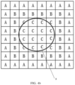
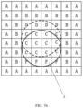
- the preset detection region is divided into 64 rectangular subregions distributed in the form of a 8 X 8 matrix, and A, B, C, D and F respectively represents the real-time detected height values corresponding to the rectangular subregions, that is, heights of the surface of the base 2 or the surface of the wafer 3 in the corresponding rectangular subregions. As shown in FIGs.
- the real-time detected height value of each of 16 first subregions covering the slot 21 is C
- the real-time detected height value of each of 20 second subregions covering an edge of the base 2 is B
- the real-time detected height value of each of the remaining 28 subregions is A.
- the real-time detected height value of each of 4 first subregions corresponding to a lapping position is F
- the real-time detected height value of each of 4 first subregions corresponding to the slot 21 is D
- the real-time detected height value of the bottom surface of the slot 21 is D.
- the detection device performs real-time and synchronous detection of the real-time detected height value corresponding to each of the rectangular subregions, which enables more elaborate and synchronous regional detection, and can reflect the difference in the real-time detected height values of different rectangular subregions more quickly and accurately
- the controller analyzes the real-time detected height value corresponding to each of the plurality of rectangular subregions, which can more effectively reflect the position of the wafer 3 and a relative positional relationship between the wafer 3 and the base 2, thereby determine whether the position status of the wafer is normal.
- the wafer 3 is generally held by a manipulator and placed in the slot 21, and if the wafer 3 cannot be completely placed in the slot 21 and is partially lapped on an edge of the slot 21, a surface of the wafer 3 may be inclined, which in turn reduces the effect of the process.
- the controller when the base 2 is in a stationary state, is further configured to calculate a difference between the real-time detected height value and the reference height value corresponding to each of the first subregions, and determine in real time whether the difference exceeds a first preset threshold, and give, in response to the difference exceeding the first preset threshold, a prompt that the wafer is not completely placed in the slot 21, to prompt an operator to adjust the position of the wafer 3 in time.
- the first preset threshold is equal to a sum of a depth of the slot 21 and a thickness of the wafer.
- the base 2 is usually rotated continuously during the process, and to prevent the wafer 3 from slipping during the rotation of the base 2, the wafer 3 should be placed in the slot 21.
- the process gas is continuously introduced and forms a gas flow, causing a risk of separating the wafer 3 from the slot 21 under the influence of the gas flow.
- the controller is further configured to calculate a difference between the real-time detected height value and the reference height value corresponding to each of the first subregions, and determine in real time whether the difference exceeds a second preset threshold, and give, in response to the difference exceeding the second preset threshold, a prompt that the wafer slides out of the slot, to prompt an operator to adjust the position of the wafer 3 in time.
- the second preset threshold is equal to a depth of the slot.
- a drive shaft 5 is typically provided below the base 2 to drive the base 2 to rotate.
- the base 2 is generally disposed at an upper end of the drive shaft 5, and since the base 2 itself has a mass, when driven to rotate by the drive shaft 5, the base 2 will apply a certain moment of inertia on the upper end of the drive shaft 5, and apply to the drive shaft 5 a force component in a direction perpendicular to an axial direction of the drive shaft 5. Therefore, if the drive shaft 5 has insufficient rigidity or the drive shaft 5 is too long, it will swing during the rotation, thereby causing swinging of the base 2 during the rotation, which may seriously affect the effect of the process on the wafer 3.
- the detection device 4 is further configured to detect in real time, when the base 2 is in the rotating state, a real-time detected three-dimensional coordinate value corresponding to each of a plurality of second subregions distributed annularly in the preset detection region.
- the plurality of second subregions distributed annularly cover an edge of the base 2.
- the controller is further configured to acquire the real-time detected three-dimensional coordinate value corresponding to each of the second subregions, compare the real-time detected three-dimensional coordinate values corresponding to the same second subregion at two adjacent time points, and determine in real time whether the base swings according to a comparison result.
- the two adjacent time points may be time points corresponding to two adjacent revolutions of rotation of the base 2.
- the plurality of second subregions distributed annularly may change along with the surface of the swinging base.
- the real-time detected three-dimensional coordinate values corresponding to a plurality of second subregions at the same position at different revolutions of rotation of the base may be detected in real time to obtain that: the shaded region is a position of the base in a three-dimensional coordinate system after rotating without swinging; and the dashed region is a position of the base in a three-dimensional coordinate system after rotating with swinging.
- the swing amplitude of the base 2 can also be calculated by calculating a variation in the real-time detected height value of each of the second subregions, i.e., by calculating a difference in a Z coordinate of the second subregion, so as to reflect whether the base 2 swings.
- the controller is further configured to determine in real time whether a difference between the real-time detected three-dimensional coordinate values of any one of the second subregions at two adjacent time points exceeds a third preset threshold, and give, in response to the difference exceeding the third preset threshold, a prompt to an operator that the base swings.
- the process chamber 1 is generally further provided therein with an infrared temperature measuring device 6 which is typically disposed above the base 2 and directly opposite to a center of the surface of the base 2. To avoid affecting the effect of the temperature detection, the detection device 4 is positioned above the base 2 and offset from the center of the surface of the base 2.
- the detection device 4 is a device with a distance detection function for detecting a distance from the detection device 4 to the surface of the base 2 and /or the wafer 3.
- the detection device 4 is, for example, an area array lidar sensor that can transmit a laser beam and receive a reflected echo, to calculate a distance from the detection device 4 to a detection target according to the time of the transmitting and receiving process.
- the area array lidar sensor can synchronously detect a plurality of first subregions distributed in an array in a preset detection region in real time, which enables more elaborate and synchronous regional detection, can reflect the difference in the real-time detected height values of different first subregions more quickly and accurately, and have the advantages of fast response speed and higher detection precision and the like.
- an industrial camera is generally used for ranging, but the illumination intensity inside the semiconductor process chamber usually cannot meet the requirements of the industrial camera, resulting in a larger error when the industrial camera is used for ranging.
- the area array lidar sensor has low requirements on the illumination intensity, and thus can obtain a more accurate detection result.
- the detection device 4 when the detection device 4 is a single area array lidar sensor, it may be considered as a point in an interior space of the process chamber 1, and then it will be readily appreciated that the surfaces of the base 2 and /or the wafer 3 in different subregions have different distances to the detection device 4 even when they have the same height. Therefore, the real-time detected distance value detected by the area array lidar sensor is not sufficient to intuitively reflect the heights of the surfaces of the base 2 and the wafer 3.
- the controller is further configured to convert a distance value obtained by the area array lidar sensor to a corresponding surface height value in real time. Specifically, taking FIG.
- the area array lidar sensor (the detection device 4) itself may be regarded as an origin, and the detection process may be regarded as a process of establishing a spherical coordinate system in a space and calculating a spherical coordinate at a certain position on the surface of the base 2.
- the controller can convert received spherical coordinates into corresponding three-dimensional coordinates. Since the conversion between the spherical coordinates and the three-dimensional coordinates is a very mature mathematical algorithm, the conversion process of the controller is not described in detail here.
- the detection device 4 is not limited to the single ranging device shown in FIG. 2 , and in some optional embodiments, the detection device may include a plurality of ranging devices above the base 2, for example, a plurality of ranging devices in one-to-one correspondence with the subregions.
- the controller may employ a programmable logic controller (PLC).
- PLC programmable logic controller
- the detection device is used to perform regional height detection on the surface of the base in real time, and the detection device can synchronously detect the plurality of first subregions distributed in an array in the preset detection region in real time, which enables more elaborate and synchronous regional detection, can reflect the difference in the real-time detected height values of different first subregions more quickly and accurately, and have the advantages of fast response and accurate detection results, and the controller is used to comprehensively analyze the real-time detected height value and the preset reference height value corresponding to each of the first subregions, to determine whether the position status of the wafer is normal, for example, whether the wafer is completely positioned in the slot in the base.
- the semiconductor processing device provided in the present disclosure can more intuitively reflect the height value and changes in the height in the preset detection region, so that the position status of the wafer in the process chamber can be reflected more quickly and accurately, the position status of the wafer can be monitored in real time, and when the wafer is separated from the slot in the process, an operator can timely make a response to ensure that the process can be smoothly carried out.
- the present embodiment provides a method for monitoring wafer position status which is applied to the semiconductor processing device as described above. As shown in Fig. 7 , the method may include the following operations S1 to S2.
- the method for monitoring wafer position status provided in the present embodiment can more quickly and accurately reflect the position status of the wafer in the process chamber, thereby enabling monitoring of the position status of the wafer in real time, so that when the wafer is separated from the slot in the process, an operator can timely make a response to ensure that the process can be smoothly carried out.
- the present embodiment provides various application flows of the semiconductor processing device and the method described above in actual processes.
- an application flow specifically includes the following operations S01 to S04.
- a height value of a surface of the base corresponding to each of a plurality of first subregions detected by the detection device is acquired and stored as a first reference height value.
- the wafer is placed in the slot, and a height value of each first subregion detected by the detection device in real time is acquired and stored as a first real-time detected height value.
- a difference between the first reference height value and the first real-time detected height value of each first subregion is calculated in real time.
- the first preset threshold is equal to a sum of a depth of the slot and a thickness of the wafer.
- an application flow specifically includes the following operations S01 to S06.
- the wafer is placed in the slot.
- the base is controlled to rotate.
- a height value of a surface of the base corresponding to each of a plurality of first subregions detected by the detection device is acquired and stored as a second reference height value.
- a height value of each first subregion detected by the detection device in real time is acquired, so as to acquire the corresponding real-time detected height value of the surface of the base and the wafer, and the height value is stored as a second real-time detected height value.
- a difference between the second reference height value and the second real-time detected height value of each second subregion is calculated in real time.
- step S06 whether the difference of any one of the second subregions exceeds a second preset threshold is determined, a prompt that the wafer slides out of the slot is given to an operator in response to the difference of any one of the second subregions exceeding the second preset threshold, and the process returns to operation S05 in response to the difference of none of the second subregions exceeding the second preset threshold.
- the second preset threshold is equal to a depth of the slot.
- an application flow specifically includes the following operations S01 to S03.
- the base is controlled to rotate.
- a three-dimensional coordinate value (including X, Y and Z values) of each second subregion detected by the detection device in real time is acquired, the real-time detected three-dimensional coordinate value in a previous one of two adjacent revolutions of rotation of the base is stored as a reference three-dimensional coordinate value, and the real-time detected three-dimensional coordinate value in a next one of the two adjacent revolutions is stored as a third real-time detected three-dimensional coordinate value.
- a plurality of second subregions distributed annularly cover an edge of the base.
- the various application processes provided in the present embodiment can more quickly and accurately reflect the position status of the wafer in the process chamber, thereby enabling monitoring of the position status of the wafer in real time, so that when the wafer is separated from the slot in the process, an operator can timely make a response to ensure that the process can be smoothly carried out.
Landscapes
- Chemical & Material Sciences (AREA)
- General Chemical & Material Sciences (AREA)
- Chemical Kinetics & Catalysis (AREA)
- Engineering & Computer Science (AREA)
- Materials Engineering (AREA)
- Metallurgy (AREA)
- Organic Chemistry (AREA)
- Mechanical Engineering (AREA)
- Crystallography & Structural Chemistry (AREA)
- Container, Conveyance, Adherence, Positioning, Of Wafer (AREA)
- Chemical Vapour Deposition (AREA)
- Testing Or Measuring Of Semiconductors Or The Like (AREA)
Abstract
Description
- The present disclosure relates to the technical field of semiconductor manufacturing, and specifically, relates to a semiconductor processing device and a method for monitoring wafer position status.
- The basic principle of the chemical vapor deposition epitaxial growth process is to deliver a process gas into a process chamber, where the process gas is heated to react in the process chamber, thereby being deposited on a wafer to form a film. During this process, the wafer is typically placed in a slot in the base so that the base can continuously rotate the wafer. If the wafer cannot be completely placed in the slot and is partially lapped on an edge of the slot, or the base swings during rotation, the uniformity of the film deposited on the surface of the wafer will be greatly reduced, which may result in a reduced yield of the product.
- The existing wafer position detection device typically detects temperature fluctuations at a central position of the base to determine whether the wafer is positioned in the slot of the base. However, due to the hysteresis of the temperature fluctuations, the existing detection device for wafer status has a low detection accuracy and untimely data feedback, making it hard to accurately reflect the position of the wafer and the rotation condition of the base in the process.
- To solve at least one of the technical problems in the existing art, the present disclosure provides a semiconductor processing device and a method for monitoring wafer position status which can more accurately reflect the position status of a wafer inside a semiconductor process chamber.
- To achieve the object of the present disclosure, there is provided a semiconductor processing device, including a process chamber in which a base for carrying a wafer is provided, wherein the base is provided with a slot for accommodating the wafer, and the process chamber is further provided with a detection device configured to detect in real time a real-time detected height value corresponding to each of a plurality of first subregions distributed in an array in a preset detection region of the process chamber; the preset detection region covers an upper surface of the base, and the plurality of first subregions cover at least the slot; the semiconductor processing device further includes a controller configured to acquire the real-time detected height value corresponding to each of the first subregions, and determine, according to the real-time detected height value corresponding to each of the first subregions and a preset reference height value, whether position status of the wafer is normal; and the reference height value is a height value corresponding to each of the plurality of first subregions detected by the detection device when both the base and the wafer carried on the base are at a standard position.
- Optionally, both the base and the wafer carried on the base being at a standard position includes: the base is at a specified levelness and the wafer is at a specified standard position on the base.
- Optionally, the controller is further configured to calculate a difference between the real-time detected height value and the reference height value corresponding to each of the first subregions, and determine in real time whether the difference exceeds a preset threshold, determine, in response to the difference not exceeding the preset threshold, that the wafer is in normal position status, and determine, in response to the difference exceeding the preset threshold, that the wafer is not in normal position status.
- Optionally, the base is rotatable; and when the base is in a stationary state, the controller is configured to calculate a difference between the real-time detected height value and the reference height value corresponding to each of the first subregions, and determine in real time whether the difference exceeds a first preset threshold, and give, in response to the difference exceeding the first preset threshold, a prompt that the wafer is not completely placed in the slot; wherein the first preset threshold is equal to a sum of a depth of the slot and a thickness of the wafer.
- Optionally, the base is rotatable; and when the base is in a rotating state, the controller is configured to calculate a difference between the real-time detected height value and the reference height value corresponding to each of the first subregions, and determine in real time whether the difference exceeds a second preset threshold, and give, in response to the difference exceeding the second preset threshold, a prompt that the wafer slides out of the slot; wherein the second preset threshold is equal to a depth of the slot.
- Optionally, the base is rotatable; and the detection device is further configured to detect in real time, when the base is in a rotating state, a real-time detected three-dimensional coordinate value corresponding to each of a plurality of second subregions distributed annularly in the preset detection region; wherein the plurality of second subregions distributed annularly cover an edge of the base; and the controller is further configured to acquire the real-time detected three-dimensional coordinate value corresponding to each of the second subregions, compare the real-time detected three-dimensional coordinate values corresponding to the same second subregion at two adjacent time points, and determine in real time whether the base swings according to a comparison result.
- Optionally, the controller is further configured to determine in real time whether a difference between the real-time detected three-dimensional coordinate values of any one of the second subregions at two adjacent time points exceeds a third preset threshold, and give, in response to the difference exceeding the third preset threshold, a prompt that the base swings.
- Optionally, a temperature measuring device is disposed above the base, wherein the temperature measuring device is directly opposite to a center of a surface of the base, and is configured to detect a temperature of the wafer; and the detection device is positioned above the base and offset from the center of the surface of the base.
- Optionally, the detection device includes an area array lidar sensor.
- As another technical solution, the present disclosure further provides a method for monitoring wafer position status, which is applicable to the semiconductor processing device according to any one of the above embodiments and includes: acquiring the real-time detected height value corresponding to each of the first subregions; and determining, according to the real-time detected height value and the reference height value corresponding to each of the first subregions, whether position status of the wafer is normal.
- The present disclosure has the following beneficial effects: in the semiconductor processing device provided in the present disclosure, the detection device is used to perform regional height detection on the surface of the base in real time, and the detection device can synchronously detect the plurality of first subregions distributed in an array in the preset detection region in real time, which enables more elaborate and synchronous regional detection, can reflect the difference in the real-time detected height values of different first subregions more quickly and accurately, and have the advantages of fast response and accurate detection results, and the controller is used to comprehensively analyze the real-time detected height value and the preset reference height value corresponding to each of the first subregions, to determine whether the position status of the wafer is normal, for example, whether the wafer is completely positioned in the slot in the base. Therefore, by combining the controller and the detection device described above, the semiconductor processing device of the present disclosure can more intuitively reflect the height value and changes in the height in the preset detection region, so that the position status of the wafer in the process chamber can be reflected more quickly and accurately, the position status of the wafer can be monitored in real time, and when the wafer is separated from the slot in the process, an operator can timely make a response to ensure that the process can be smoothly carried out.
- When applied to the semiconductor processing device as described above, the method for monitoring wafer position status according to the embodiments of the present disclosure can more quickly and accurately reflect the position status of the wafer in the process chamber, thereby enabling monitoring of the position status of the wafer in real time, so that when the wafer is separated from the slot in the process, an operator can timely make a response to ensure that the process can be smoothly carried out.
-
-
FIG. 1 is a simplified diagram of a chemical vapor deposition epitaxial growth process chamber; -
FIG. 2 is a schematic structural diagram of a semiconductor processing device according to a first embodiment; -
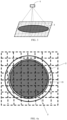
FIG. 3 is a schematic diagram of a preset detection region of the detection device according to the first embodiment; -
FIG. 4a is a top view of a base when a wafer is completely positioned in a slot; -
FIG. 4b is a diagram showing distribution of detection results when the wafer is completely positioned in the slot; -
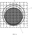
FIG. 5a is a top view of a base when a wafer is not completely positioned in a slot; -
FIG. 5b is a diagram showing distribution of detection results when the wafer is not completely positioned in the slot; -
FIG. 6 is a spatial position diagram of the base when the base does not swing and when the base swings; and -
FIG. 7 is a flowchart of a monitoring method according to a second embodiment. - To better understand the technical solution of the present disclosure for those skilled in the art, the semiconductor processing device and the method for monitoring wafer position status provided in the present disclosure will be described in detail below in conjunction with the accompanying drawings.
- As shown in
FIG. 1 , a chemical vapor deposition epitaxial growth process device typically includes: aprocess chamber 1, and abase 2 and a heat source (not shown) provided in theprocess chamber 1. When the chemical vapor deposition epitaxial process is started, a wafer is placed in a slot in thebase 2, while a process gas enters theprocess chamber 1 through a gas inlet 11 and flows out of theprocess chamber 1 through agas outlet 12, and reacts in theprocess chamber 1 under heating. The product of the reaction is deposited on a surface of the wafer under the action of gravity to form a film. Since the material forming the film is deposited only by gravity, the wafer should be kept as level as possible to improve the uniformity of the film. In the actual process, however, there are various situations that may affect levelness of the wafer, for example: the wafer may be not completely placed in the slot in thebase 2, or thebase 2 may swing during rotation. If an operator cannot adjust the position of the wafer in time before or during such a situation, the effect of the process will be significant reduced, even causing failure of the process. - To solve the above technical problem, the present embodiment provides a semiconductor processing device for reflecting position status of a wafer in the semiconductor processing device in real time during the process. Specifically, the semiconductor processing device in the present embodiment is not limited to a chemical vapor deposition epitaxial growth processing device, and may be a processing device such as a physical vapor deposition processing device or an atomic layer deposition processing device that has certain requirements on the levelness of the wafer.
- Referring to
FIG. 2 , the semiconductor processing device provided in the present embodiment includes: aprocess chamber 1, abase 2 for carrying awafer 3, adetection device 4 and a controller (not shown in the figure). Thebase 2 is disposed in theprocess chamber 1, and aslot 21 for accommodating the wafer is provided in thebase 2. Thedetection device 4 has a function of detecting a surface height of a target object. Specifically, thedetection device 4 is configured to detect in real time real-time detected height values corresponding to a plurality of first subregions distributed in an array in a preset detection region of theprocess chamber 1, and send the real-time detected height values to the controller. It should be noted that the real-time detected height value corresponding to each of the first subregions includes one or more of a real-time detected height value of a surface of thebase 2, a real-time detected height value of a surface of thewafer 3, and a real-time detected height value of a bottom surface of theslot 21. - Moreover, as shown in
FIGs. 2 and3 , the preset detection region completely covers at least an upper surface of thebase 2, and the plurality of first subregions cover at least theslot 21, thereby enabling regional real-time detection on the height of the surface of theslot 21 and /or the height of the surface of thewafer 3 placed in theslot 21 at different positions. - The controller is configured to pre-store a preset reference height value corresponding to each of the first subregions. Specifically, the reference height value is a height value corresponding to each of the plurality of first subregions detected by the
detection device 4 when both thebase 2 and thewafer 3 carried on thebase 2 are at a standard position. The controller is further configured to acquire the real-time detected height value corresponding to each of the first subregions, and determine, according to the real-time detected height value and the preset reference height value corresponding to each of the first subregions, whether position status of the wafer is normal, that is, determine whether thewafer 3 is at an expected position during the process by comprehensively analyzing the real-time detected height value and the reference height value corresponding to each of the first subregions. - Further, the detection device can synchronously detect the plurality of first subregions distributed in an array in the preset detection region in real time, which enables more elaborate and synchronous regional detection, can reflect the difference in the real-time detected height values of different first subregions more quickly and accurately, and have the advantages of fast response and accurate detection results. Therefore, by combining the controller and the
detection device 4 described above, the height value and changes in the height in the preset detection region can be more intuitively reflected, so that the position status of the wafer in the process chamber can be reflected more quickly and accurately, the position status of the wafer can be monitored in real time, and when the wafer is separated from the slot in the process, an operator can timely make a response to ensure that the process can be smoothly carried out. - It should be noted that the preset detection region is a region detectable by the detection device, which is a virtual region representing a detection range. The plurality of first subregions are also subregions virtually divided by the detection device, and represent an array regional detection mode.
- The reference height value should be collected when the
base 2 and thewafer 3 are both at a preset standard position. Specifically, in some optional embodiments, the standard position includes: a position where thebase 2 is at a specified levelness and thewafer 3 is at a specified standard position on thebase 2. Accordingly, the reference height value includes: a height value of a surface of thebase 4 detected by thedetection device 4 when thebase 2 is at a specified levelness; and/or height values of a surface of thewafer 3 and a surface of thebase 2 when thewafer 3 is at the specified standard position. In addition, the standard position may be selected according to normal position status of thewafer 3 expected during the process. For example, as shown inFIG. 2 , to determine whether thewafer 3 is placed in theslot 21 in thebase 2, a position of thebase 2 without the wafer (i.e., when theslot 21 is empty) may be used as the standard position, and thus, a height of a bottom surface of theslot 21 is used as the reference height value. - In some optional embodiments, the controller is further configured to calculate a difference between the real-time detected height value and the reference height value corresponding to each of the first subregions, and determine in real time whether the difference exceeds a preset threshold, determine, in response to the difference not exceeding the preset threshold, that the
wafer 3 is in normal position status, and determine, in response to the difference exceeding the preset threshold, that thewafer 3 is not in normal position status. - Taking
FIGs. 4a to 5b as an example, where various types of wafer position status and corresponding height value detection results are shown, the preset detection region is divided into 64 rectangular subregions distributed in the form of a 8 X 8 matrix, and A, B, C, D and F respectively represents the real-time detected height values corresponding to the rectangular subregions, that is, heights of the surface of thebase 2 or the surface of thewafer 3 in the corresponding rectangular subregions. As shown inFIGs. 4a and4b , when thewafer 3 is completely positioned in theslot 21 in thebase 2, the real-time detected height value of each of 16 first subregions covering theslot 21 is C, the real-time detected height value of each of 20 second subregions covering an edge of thebase 2 is B, and the real-time detected height value of each of the remaining 28 subregions is A. As shown inFIGs. 5a and5b , when thewafer 3 is not completely positioned in theslot 21, thewafer 3 is partially lapped on the edge of theslot 21, the real-time detected height value of each of 4 first subregions corresponding to a lapping position is F, and the real-time detected height value of each of 4 first subregions corresponding to theslot 21 is D, that is, the real-time detected height value of the bottom surface of theslot 21 is D. It can be seen that the detection device performs real-time and synchronous detection of the real-time detected height value corresponding to each of the rectangular subregions, which enables more elaborate and synchronous regional detection, and can reflect the difference in the real-time detected height values of different rectangular subregions more quickly and accurately, and the controller analyzes the real-time detected height value corresponding to each of the plurality of rectangular subregions, which can more effectively reflect the position of thewafer 3 and a relative positional relationship between thewafer 3 and thebase 2, thereby determine whether the position status of the wafer is normal. - At the beginning of the process, the
wafer 3 is generally held by a manipulator and placed in theslot 21, and if thewafer 3 cannot be completely placed in theslot 21 and is partially lapped on an edge of theslot 21, a surface of thewafer 3 may be inclined, which in turn reduces the effect of the process. To solve this technical problem, in some optional embodiments, when thebase 2 is in a stationary state, the controller is further configured to calculate a difference between the real-time detected height value and the reference height value corresponding to each of the first subregions, and determine in real time whether the difference exceeds a first preset threshold, and give, in response to the difference exceeding the first preset threshold, a prompt that the wafer is not completely placed in theslot 21, to prompt an operator to adjust the position of thewafer 3 in time. The first preset threshold is equal to a sum of a depth of theslot 21 and a thickness of the wafer. It will be readily appreciated that when thewafer 3 is partially lapped on the edge of thebase 2, a height difference between the surface of thewafer 3 and the bottom surface of theslot 21 at the lapping position is inevitably greater than or equal to the sum of the depth of theslot 21 and the thickness of thewafer 3, so that once the difference exceeds the first preset threshold, it can be determined that the wafer is not completely placed in theslot 21. - In the actual process, to ensure uniform heating of the
wafer 3, thebase 2 is usually rotated continuously during the process, and to prevent thewafer 3 from slipping during the rotation of thebase 2, thewafer 3 should be placed in theslot 21. However, during the process, the process gas is continuously introduced and forms a gas flow, causing a risk of separating thewafer 3 from theslot 21 under the influence of the gas flow. To monitor the position of thewafer 3, in some optional embodiments, when thebase 2 is in a rotating state, the controller is further configured to calculate a difference between the real-time detected height value and the reference height value corresponding to each of the first subregions, and determine in real time whether the difference exceeds a second preset threshold, and give, in response to the difference exceeding the second preset threshold, a prompt that the wafer slides out of the slot, to prompt an operator to adjust the position of thewafer 3 in time. Specifically, the second preset threshold is equal to a depth of the slot. It will be readily appreciated that when thewafer 3 slides out of theslot 21, thewafer 3 will be partially or entirely lapped on the edge of theslot 21, and a height difference between the surface of thewafer 3 at the lapping position and a surface of thewafer 3 completely placed in theslot 21 is inevitably greater than or equal to the depth of theslot 21, so that once the difference exceeds the second preset threshold, it can be determined that the wafer slides out of the slot. - As shown in
FIG. 1 , a drive shaft 5 is typically provided below thebase 2 to drive thebase 2 to rotate. Thebase 2 is generally disposed at an upper end of the drive shaft 5, and since thebase 2 itself has a mass, when driven to rotate by the drive shaft 5, thebase 2 will apply a certain moment of inertia on the upper end of the drive shaft 5, and apply to the drive shaft 5 a force component in a direction perpendicular to an axial direction of the drive shaft 5. Therefore, if the drive shaft 5 has insufficient rigidity or the drive shaft 5 is too long, it will swing during the rotation, thereby causing swinging of thebase 2 during the rotation, which may seriously affect the effect of the process on thewafer 3. - To monitor a rotating state of the
base 2, in some optional embodiments, thedetection device 4 is further configured to detect in real time, when thebase 2 is in the rotating state, a real-time detected three-dimensional coordinate value corresponding to each of a plurality of second subregions distributed annularly in the preset detection region. The plurality of second subregions distributed annularly cover an edge of thebase 2. The controller is further configured to acquire the real-time detected three-dimensional coordinate value corresponding to each of the second subregions, compare the real-time detected three-dimensional coordinate values corresponding to the same second subregion at two adjacent time points, and determine in real time whether the base swings according to a comparison result. Specifically, in some optional embodiments, the two adjacent time points may be time points corresponding to two adjacent revolutions of rotation of thebase 2. - It should be noted that if the base swings, the plurality of second subregions distributed annularly (i.e., detection objects of the detection device) may change along with the surface of the swinging base. Referring to
FIG. 6 , when thebase 2 is rotated, the real-time detected three-dimensional coordinate values corresponding to a plurality of second subregions at the same position at different revolutions of rotation of the base may be detected in real time to obtain that: the shaded region is a position of the base in a three-dimensional coordinate system after rotating without swinging; and the dashed region is a position of the base in a three-dimensional coordinate system after rotating with swinging. Comparing the two regions, it can be seen that an X value and /or a Y value of the corresponding second subregion when thebase 2 swings are/is changed compared with the case where the base does not swing, so that differences in the X value and the Y value of the second subregion can be calculated to calculate a swing amplitude of thebase 2. - In addition, as can be seen from
FIGs. 1 and6 , when thebase 2 swings during the rotation, a surface height at the edge of thebase 2 is greatly changed, so that thedetection device 4 can easily detect changes in the detected heights of the plurality of second subregions at the edge of thebase 2. Accordingly, if a diameter of thebase 2 and a length of the drive shaft 5 are given in actual production, the swing amplitude of thebase 2 can also be calculated by calculating a variation in the real-time detected height value of each of the second subregions, i.e., by calculating a difference in a Z coordinate of the second subregion, so as to reflect whether thebase 2 swings. - In some optional embodiments, the controller is further configured to determine in real time whether a difference between the real-time detected three-dimensional coordinate values of any one of the second subregions at two adjacent time points exceeds a third preset threshold, and give, in response to the difference exceeding the third preset threshold, a prompt to an operator that the base swings.
- In some optional embodiments, the
process chamber 1 is generally further provided therein with an infraredtemperature measuring device 6 which is typically disposed above thebase 2 and directly opposite to a center of the surface of thebase 2. To avoid affecting the effect of the temperature detection, thedetection device 4 is positioned above thebase 2 and offset from the center of the surface of thebase 2. - In some optional embodiments, the
detection device 4 is a device with a distance detection function for detecting a distance from thedetection device 4 to the surface of thebase 2 and /or thewafer 3. Thedetection device 4 is, for example, an area array lidar sensor that can transmit a laser beam and receive a reflected echo, to calculate a distance from thedetection device 4 to a detection target according to the time of the transmitting and receiving process. The area array lidar sensor can synchronously detect a plurality of first subregions distributed in an array in a preset detection region in real time, which enables more elaborate and synchronous regional detection, can reflect the difference in the real-time detected height values of different first subregions more quickly and accurately, and have the advantages of fast response speed and higher detection precision and the like. Moreover, in the existing art, an industrial camera is generally used for ranging, but the illumination intensity inside the semiconductor process chamber usually cannot meet the requirements of the industrial camera, resulting in a larger error when the industrial camera is used for ranging. Compared with the existing art, the area array lidar sensor has low requirements on the illumination intensity, and thus can obtain a more accurate detection result. - Taking
FIG. 2 as an example, when thedetection device 4 is a single area array lidar sensor, it may be considered as a point in an interior space of theprocess chamber 1, and then it will be readily appreciated that the surfaces of thebase 2 and /or thewafer 3 in different subregions have different distances to thedetection device 4 even when they have the same height. Therefore, the real-time detected distance value detected by the area array lidar sensor is not sufficient to intuitively reflect the heights of the surfaces of thebase 2 and thewafer 3. To acquire the heights of the surfaces of thebase 2 and thewafer 3 more intuitively, in some optional embodiments, the controller is further configured to convert a distance value obtained by the area array lidar sensor to a corresponding surface height value in real time. Specifically, takingFIG. 2 as an example, when performing detection, the area array lidar sensor (the detection device 4) itself may be regarded as an origin, and the detection process may be regarded as a process of establishing a spherical coordinate system in a space and calculating a spherical coordinate at a certain position on the surface of thebase 2. Accordingly, the controller can convert received spherical coordinates into corresponding three-dimensional coordinates. Since the conversion between the spherical coordinates and the three-dimensional coordinates is a very mature mathematical algorithm, the conversion process of the controller is not described in detail here. - It should be further noted that the
detection device 4 is not limited to the single ranging device shown inFIG. 2 , and in some optional embodiments, the detection device may include a plurality of ranging devices above thebase 2, for example, a plurality of ranging devices in one-to-one correspondence with the subregions. - In some optional embodiments, the controller may employ a programmable logic controller (PLC).
- In the semiconductor processing device provided in the present embodiment, the detection device is used to perform regional height detection on the surface of the base in real time, and the detection device can synchronously detect the plurality of first subregions distributed in an array in the preset detection region in real time, which enables more elaborate and synchronous regional detection, can reflect the difference in the real-time detected height values of different first subregions more quickly and accurately, and have the advantages of fast response and accurate detection results, and the controller is used to comprehensively analyze the real-time detected height value and the preset reference height value corresponding to each of the first subregions, to determine whether the position status of the wafer is normal, for example, whether the wafer is completely positioned in the slot in the base. Therefore, by combining the controller and the detection device described above, the semiconductor processing device provided in the present disclosure can more intuitively reflect the height value and changes in the height in the preset detection region, so that the position status of the wafer in the process chamber can be reflected more quickly and accurately, the position status of the wafer can be monitored in real time, and when the wafer is separated from the slot in the process, an operator can timely make a response to ensure that the process can be smoothly carried out.
- Based on the semiconductor processing device provided in the first embodiment, the present embodiment provides a method for monitoring wafer position status which is applied to the semiconductor processing device as described above. As shown in
Fig. 7 , the method may include the following operations S1 to S2. - At
operation S 1, the real-time detected height value corresponding to each of the first subregions is acquired. - At operation S2, whether position status of the wafer is normal is determined according to the real-time detected height value and the reference height value corresponding to each of the first subregions.
- The method for monitoring wafer position status provided in the present embodiment can more quickly and accurately reflect the position status of the wafer in the process chamber, thereby enabling monitoring of the position status of the wafer in real time, so that when the wafer is separated from the slot in the process, an operator can timely make a response to ensure that the process can be smoothly carried out.
- Based on the semiconductor processing device provided in the first embodiment and the method for monitoring wafer position status provided in the second embodiment, the present embodiment provides various application flows of the semiconductor processing device and the method described above in actual processes.
- To monitor whether the wafer is completely placed in the slot at the beginning of the process, in some optional embodiments, an application flow specifically includes the following operations S01 to S04.
- At operation S01, before the process starts, a height value of a surface of the base corresponding to each of a plurality of first subregions detected by the detection device is acquired and stored as a first reference height value.
- At operation S02, in a process starting stage, the wafer is placed in the slot, and a height value of each first subregion detected by the detection device in real time is acquired and stored as a first real-time detected height value.
- At operation S03, a difference between the first reference height value and the first real-time detected height value of each first subregion is calculated in real time.
- At operation S04, whether the difference of any one of the first subregions exceeds a first preset threshold is determined, a prompt that the wafer is not completely placed in the slot is given to an operator in response to the difference of any one of the first subregions exceeding the first preset threshold, and the process returns to operation S02 in response to the difference of none of the first subregions exceeding the first preset threshold. Specifically, the first preset threshold is equal to a sum of a depth of the slot and a thickness of the wafer.
- To monitor whether the wafer is separated from the slot during the rotation of the base, in some optional embodiments, an application flow specifically includes the following operations S01 to S06.
- At operation S01, the wafer is placed in the slot.
- At operation S02, the base is controlled to rotate.
- At operation S03, during a first revolution of the base, a height value of a surface of the base corresponding to each of a plurality of first subregions detected by the detection device is acquired and stored as a second reference height value.
- At operation S04, during subsequent rotation of the base, a height value of each first subregion detected by the detection device in real time is acquired, so as to acquire the corresponding real-time detected height value of the surface of the base and the wafer, and the height value is stored as a second real-time detected height value.
- At operation S05, a difference between the second reference height value and the second real-time detected height value of each second subregion is calculated in real time.
- At step S06, whether the difference of any one of the second subregions exceeds a second preset threshold is determined, a prompt that the wafer slides out of the slot is given to an operator in response to the difference of any one of the second subregions exceeding the second preset threshold, and the process returns to operation S05 in response to the difference of none of the second subregions exceeding the second preset threshold. Specifically, the second preset threshold is equal to a depth of the slot.
- To monitor whether the base swings greatly during the rotation, in some optional embodiments, an application flow specifically includes the following operations S01 to S03.
- At operation S01, the base is controlled to rotate.
- At operation S02, during each revolution of the base, a three-dimensional coordinate value (including X, Y and Z values) of each second subregion detected by the detection device in real time is acquired, the real-time detected three-dimensional coordinate value in a previous one of two adjacent revolutions of rotation of the base is stored as a reference three-dimensional coordinate value, and the real-time detected three-dimensional coordinate value in a next one of the two adjacent revolutions is stored as a third real-time detected three-dimensional coordinate value.
- Specifically, a plurality of second subregions distributed annularly cover an edge of the base.
- At operation S03, it is determined in real time whether a reference three-dimensional coordinate value of the surface of the base in any subregion at the edge of the base is different from the real-time detected three-dimensional coordinate value, a prompt that the base swings is given to an operator and differences between the reference three-dimensional coordinate values of the surface of the base in the plurality of subregion at the edge of the base and the real-time detected three-dimensional coordinate values are calculated in response to the reference three-dimensional coordinate value of the surface of the base in any subregion at the edge of the base being different from the real-time detected three-dimensional coordinate value, and the differences are stored as variations of the real-time detected three-dimensional coordinate values; otherwise, the process returns to step S02.
- By combining the method provided in the second embodiment with the semiconductor processing device provided in the first embodiment, the various application processes provided in the present embodiment can more quickly and accurately reflect the position status of the wafer in the process chamber, thereby enabling monitoring of the position status of the wafer in real time, so that when the wafer is separated from the slot in the process, an operator can timely make a response to ensure that the process can be smoothly carried out.
- It will be appreciated that the above implementations are merely exemplary implementations for the purpose of illustrating the principle of the present disclosure, and the present disclosure is not limited thereto. It will be apparent to one of ordinary skill in the art that various modifications and variations may be made without departing from the spirit or essence of the present disclosure. Such modifications and variations should also be considered as falling into the protection scope of the present disclosure.
Claims (10)
- A semiconductor processing device, comprising a process chamber in which a base for carrying a wafer is provided, the base being provided with a slot for accommodating the wafer, whereinthe process chamber is further provided with a detection device configured to detect in real time a real-time detected height value corresponding to each of a plurality of first subregions distributed in an array in a preset detection region of the process chamber; the preset detection region covers an upper surface of the base, and the plurality of first subregions cover at least the slot;the semiconductor processing device further comprises a controller configured to acquire the real-time detected height value corresponding to each of the plurality of first subregions, and determine, according to the real-time detected height value corresponding to each of the plurality of first subregions and a preset reference height value, whether position status of the wafer is normal; and the reference height value is a height value corresponding to each of the plurality of first subregions detected by the detection device in a case where both the base and the wafer carried on the base are at a standard position.
- The semiconductor processing device according to claim 1, wherein both the base and the wafer carried on the base being at a standard position comprises: the base is at a specified levelness and the wafer is at a specified standard position on the base.
- The semiconductor processing device according to claim 1, wherein the controller is further configured to calculate a difference between the real-time detected height value and the reference height value corresponding to each of the plurality of first subregions, and determine in real time whether the difference exceeds a preset threshold, determine, in response to the difference not exceeding the preset threshold, that the wafer is in normal position status, and determine, in response to the difference exceeding the preset threshold, that the wafer is not in normal position status.
- The semiconductor processing device according to claim 3, wherein the base is rotatable; andwhen the base is in a stationary state, the controller is configured to calculate a difference between the real-time detected height value and the reference height value corresponding to each of the plurality of first subregions, and determine in real time whether the difference exceeds a first preset threshold, and give, in response to the difference exceeding the first preset threshold, a prompt that the wafer is not completely placed in the slot; whereinthe first preset threshold is equal to a sum of a depth of the slot and a thickness of the wafer.
- The semiconductor processing device according to claim 3, wherein the base is rotatable; andwhen the base is in a rotating state, the controller is configured to calculate a difference between the real-time detected height value and the reference height value corresponding to each of the plurality of first subregions, and determine in real time whether the difference exceeds a second preset threshold, and give, in response to the difference exceeding the second preset threshold, a prompt that the wafer slides out of the slot; whereinthe second preset threshold is equal to a depth of the slot.
- The semiconductor processing device according to any of claims 1 to 5, wherein the base is rotatable;the detection device is further configured to detect in real time, when the base is in a rotating state, a real-time detected three-dimensional coordinate value corresponding to each of a plurality of second subregions distributed annularly in the preset detection region; wherein the plurality of second subregions distributed annularly cover an edge of the base; andthe controller is further configured to acquire the real-time detected three-dimensional coordinate value corresponding to each of the plurality of second subregions, compare the real-time detected three-dimensional coordinate values corresponding to the same second subregion at two adjacent time points, and determine in real time whether the base swings according to a comparison result.
- The semiconductor processing device according to claim 6, wherein the controller is further configured to determine in real time whether a difference between the real-time detected three-dimensional coordinate values of any one of the plurality of second subregions at two adjacent time points exceeds a third preset threshold, and give, in response to the difference exceeding the third preset threshold, a prompt that the base swings.
- The semiconductor processing device according to claim 1, wherein a temperature measuring device is disposed above the base, the temperature measuring device is directly opposite to a center of a surface of the base, and is configured to detect a temperature of the wafer; and
the detection device is positioned above the base and offset from the center of the surface of the base. - The semiconductor processing device according to claim 1, wherein the detection device comprises an area array lidar sensor.
- A method for monitoring wafer position status, applied to the semiconductor processing device according to any one of claims 1 to 9, comprising:acquiring the real-time detected height value corresponding to each of the plurality of first subregions; anddetermining, according to the real-time detected height value and the reference height value corresponding to each of the plurality of first subregions, whether position status of the wafer is normal.
Applications Claiming Priority (2)
| Application Number | Priority Date | Filing Date | Title |
|---|---|---|---|
| CN202111271410.6A CN114000192B (en) | 2021-10-29 | 2021-10-29 | Semiconductor process equipment and methods for monitoring wafer position status |
| PCT/CN2022/127886 WO2023072180A1 (en) | 2021-10-29 | 2022-10-27 | Semiconductor processing device and method for monitoring wafer position status |
Publications (2)
| Publication Number | Publication Date |
|---|---|
| EP4424887A1 true EP4424887A1 (en) | 2024-09-04 |
| EP4424887A4 EP4424887A4 (en) | 2025-07-30 |
Family
ID=79925498
Family Applications (1)
| Application Number | Title | Priority Date | Filing Date |
|---|---|---|---|
| EP22886055.7A Pending EP4424887A4 (en) | 2021-10-29 | 2022-10-27 | SEMICONDUCTOR PROCESSING DEVICE AND WAFER POSITION STATE MONITORING METHOD |
Country Status (5)
| Country | Link |
|---|---|
| EP (1) | EP4424887A4 (en) |
| KR (1) | KR102718266B1 (en) |
| CN (1) | CN114000192B (en) |
| TW (1) | TWI827326B (en) |
| WO (1) | WO2023072180A1 (en) |
Families Citing this family (15)
| Publication number | Priority date | Publication date | Assignee | Title |
|---|---|---|---|---|
| CN114000192B (en) * | 2021-10-29 | 2023-10-13 | 北京北方华创微电子装备有限公司 | Semiconductor process equipment and methods for monitoring wafer position status |
| US12456614B2 (en) | 2022-05-27 | 2025-10-28 | Applied Materials, Inc. | Process kits and related methods for processing chambers to facilitate deposition process adjustability |
| US12221696B2 (en) | 2022-05-27 | 2025-02-11 | Applied Materials, Inc. | Process kits and related methods for processing chambers to facilitate deposition process adjustability |
| US12428731B2 (en) | 2022-07-12 | 2025-09-30 | Applied Materials, Inc. | Flow guide structures and heat shield structures, and related methods, for deposition uniformity and process adjustability |
| US12467144B2 (en) | 2022-10-27 | 2025-11-11 | Applied Materials, Inc. | Methods of correlating zones of processing chambers, and related systems and methods |
| US12243761B2 (en) | 2022-10-27 | 2025-03-04 | Applied Materials, Inc. | Detection and analysis of substrate support and pre-heat ring in a process chamber via imaging |
| CN115435752A (en) * | 2022-11-03 | 2022-12-06 | 西安奕斯伟材料科技有限公司 | Level detection device and level detection method |
| CN115910866B (en) * | 2022-12-07 | 2026-04-28 | 西安奕斯伟材料科技股份有限公司 | A method and apparatus for controlling the production of epitaxial wafers |
| US12428753B2 (en) | 2022-12-14 | 2025-09-30 | Applied Materials, Inc. | Lift assemblies, and related methods and components, for substrate processing chambers |
| CN119061384B (en) * | 2023-05-30 | 2025-11-11 | 北京北方华创微电子装备有限公司 | Semiconductor process chamber and semiconductor process equipment |
| CN119920717B (en) * | 2023-10-31 | 2025-12-12 | 北京北方华创微电子装备有限公司 | Temperature control system, process chamber and cleaning method |
| US12540400B2 (en) | 2023-11-02 | 2026-02-03 | Applied Materials, Inc. | Multi-flow gas circuits, processing chambers, and related apparatus and methods for semiconductor manufacturing |
| CN117524880B (en) * | 2023-11-16 | 2024-07-23 | 深圳市昇维旭技术有限公司 | Semiconductor device manufacturing method and semiconductor device |
| CN117778980A (en) * | 2023-12-25 | 2024-03-29 | 上海集成电路装备材料产业创新中心有限公司 | A level monitoring system and method for heating base and process equipment |
| CN119890091A (en) * | 2024-08-30 | 2025-04-25 | 一塔半导体(安徽)有限公司 | Satellite disk rotating speed measuring system and method of multi-piece planetary MOCVD equipment |
Family Cites Families (20)
| Publication number | Priority date | Publication date | Assignee | Title |
|---|---|---|---|---|
| JP4059690B2 (en) * | 2002-02-28 | 2008-03-12 | オリンパス株式会社 | Wafer centering apparatus and method, program, wafer transfer apparatus, and inspection apparatus |
| US7352198B2 (en) * | 2006-01-18 | 2008-04-01 | Electroglas, Inc. | Methods and apparatuses for improved stabilization in a probing system |
| JP2009543355A (en) * | 2006-07-03 | 2009-12-03 | アプライド マテリアルズ インコーポレイテッド | Cluster tools for advanced front-end processing |
| WO2008079742A2 (en) * | 2006-12-20 | 2008-07-03 | Applied Materials, Inc. | Prevention of film deposition on pecvd process chamber wall |
| CN101452817B (en) * | 2007-11-30 | 2011-06-01 | 中芯国际集成电路制造(上海)有限公司 | Method for monitoring obliteration of wafer support platform and corresponding system |
| DE102009010555A1 (en) * | 2009-02-25 | 2010-09-02 | Siltronic Ag | Method for detecting a misalignment of a semiconductor wafer during a thermal treatment |
| JP6046933B2 (en) * | 2012-07-10 | 2016-12-21 | 株式会社荏原製作所 | Polishing method |
| CN104916560B (en) * | 2014-03-11 | 2018-05-25 | 北京北方华创微电子装备有限公司 | Chip detection system, reaction chamber and chip detection method |
| US10196741B2 (en) * | 2014-06-27 | 2019-02-05 | Applied Materials, Inc. | Wafer placement and gap control optimization through in situ feedback |
| US20160240419A1 (en) * | 2015-02-13 | 2016-08-18 | Eastman Kodak Company | Atomic-layer deposition substrate |
| US10124492B2 (en) * | 2015-10-22 | 2018-11-13 | Lam Research Corporation | Automated replacement of consumable parts using end effectors interfacing with plasma processing system |
| US10062599B2 (en) * | 2015-10-22 | 2018-08-28 | Lam Research Corporation | Automated replacement of consumable parts using interfacing chambers |
| CN108630563B (en) * | 2017-03-17 | 2020-11-03 | 中芯国际集成电路制造(上海)有限公司 | Monitoring method and monitoring structure of wafer identification code |
| CN208478299U (en) * | 2018-06-26 | 2019-02-05 | 德淮半导体有限公司 | A kind of wafer position detecting system |
| US11131541B2 (en) * | 2018-06-29 | 2021-09-28 | Taiwan Semiconductor Manufacturing Co., Ltd. | Shutter monitoring system |
| CN110797277B (en) * | 2018-08-01 | 2022-05-27 | 北京北方华创微电子装备有限公司 | Silicon wafer position detection method and device and semiconductor processing equipment |
| CN109375237B (en) * | 2018-12-12 | 2019-11-19 | 北京华科博创科技有限公司 | A kind of all solid state face array three-dimensional imaging laser radar system |
| KR20200117796A (en) * | 2019-04-05 | 2020-10-14 | 주성엔지니어링(주) | Apparatus for processing substrate and method for processing substrate using the same |
| CN111640685B (en) * | 2020-06-04 | 2024-06-21 | 北京北方华创微电子装备有限公司 | Semiconductor equipment and workpiece status detection method |
| CN114000192B (en) * | 2021-10-29 | 2023-10-13 | 北京北方华创微电子装备有限公司 | Semiconductor process equipment and methods for monitoring wafer position status |
-
2021
- 2021-10-29 CN CN202111271410.6A patent/CN114000192B/en active Active
-
2022
- 2022-10-27 WO PCT/CN2022/127886 patent/WO2023072180A1/en not_active Ceased
- 2022-10-27 EP EP22886055.7A patent/EP4424887A4/en active Pending
- 2022-10-27 KR KR1020247014822A patent/KR102718266B1/en active Active
- 2022-10-27 TW TW111140871A patent/TWI827326B/en active
Also Published As
| Publication number | Publication date |
|---|---|
| CN114000192B (en) | 2023-10-13 |
| TW202318526A (en) | 2023-05-01 |
| EP4424887A4 (en) | 2025-07-30 |
| WO2023072180A1 (en) | 2023-05-04 |
| TWI827326B (en) | 2023-12-21 |
| KR102718266B1 (en) | 2024-10-17 |
| CN114000192A (en) | 2022-02-01 |
| KR20240089304A (en) | 2024-06-20 |
Similar Documents
| Publication | Publication Date | Title |
|---|---|---|
| EP4424887A1 (en) | Semiconductor processing device and method for monitoring wafer position status | |
| US9604363B2 (en) | Object pickup device and method for picking up object | |
| US12215966B2 (en) | Methods and systems of optical inspection of electronic device manufacturing machines | |
| TW201615905A (en) | System and method for performing a wet etching process | |
| JP2018117116A (en) | Feature enforcement method from spectral time series to control processing endpoints | |
| US11621187B2 (en) | Systems and methods for controlling substrate approach toward a target horizontal plane | |
| CN104752295B (en) | The handling method of position monitoring device, plasma processing device and workpiece | |
| US20170287793A1 (en) | Apparatus and method to control etch rate through adaptive spiking of chemistry | |
| US11378426B2 (en) | System and method for monitoring sensor linearity as part of a production process | |
| US20200243352A1 (en) | Intelligent customizable wet processing system | |
| CN113226668A (en) | Method and device for production line simulation | |
| JP2006084294A (en) | Semiconductor wafer defect detection system | |
| CN119517810B (en) | A hole-plugging device, a hole-plugging method, and a wafer processing equipment. | |
| US20150261203A1 (en) | Semiconductor wafer position display system, semiconductor wafer position display method, and semiconductor wafer position display program | |
| CN120023922A (en) | A height correction method and system based on machine vision measurement | |
| CN117392182B (en) | Film pasting precision detection method, device, equipment and storage medium | |
| US12400887B2 (en) | Method and system of operating substrate processing by calculating wafer thickness out of wafer mapping process | |
| US6374149B1 (en) | System and method for determining the center of a wafer on a wafer table | |
| US20050244047A1 (en) | Stop motion imaging detection system and method | |
| US20240321649A1 (en) | On-the-fly measurement of substrate structures | |
| TW202613353A (en) | Utilizing infrared data for control of fabrication processes | |
| WO2024097569A1 (en) | Methods and systems for monitoring metrology fleet productivity |
Legal Events
| Date | Code | Title | Description |
|---|---|---|---|
| STAA | Information on the status of an ep patent application or granted ep patent |
Free format text: STATUS: THE INTERNATIONAL PUBLICATION HAS BEEN MADE |
|
| PUAI | Public reference made under article 153(3) epc to a published international application that has entered the european phase |
Free format text: ORIGINAL CODE: 0009012 |
|
| STAA | Information on the status of an ep patent application or granted ep patent |
Free format text: STATUS: REQUEST FOR EXAMINATION WAS MADE |
|
| 17P | Request for examination filed |
Effective date: 20240510 |
|
| AK | Designated contracting states |
Kind code of ref document: A1 Designated state(s): AL AT BE BG CH CY CZ DE DK EE ES FI FR GB GR HR HU IE IS IT LI LT LU LV MC ME MK MT NL NO PL PT RO RS SE SI SK SM TR |
|
| DAV | Request for validation of the european patent (deleted) | ||
| DAX | Request for extension of the european patent (deleted) | ||
| REG | Reference to a national code |
Ref country code: DE Ref legal event code: R079 Free format text: PREVIOUS MAIN CLASS: C30B0025080000 Ipc: C23C0016458000 |
|
| A4 | Supplementary search report drawn up and despatched |
Effective date: 20250701 |
|
| RIC1 | Information provided on ipc code assigned before grant |
Ipc: C23C 16/458 20060101AFI20250625BHEP Ipc: H01L 21/67 20060101ALI20250625BHEP Ipc: H01L 21/687 20060101ALI20250625BHEP Ipc: C23C 16/52 20060101ALI20250625BHEP |
|
| REG | Reference to a national code |
Ref country code: DE Ref legal event code: R079 Free format text: PREVIOUS MAIN CLASS: C23C0016458000 Ipc: H10P0072000000 |
|
| RIC1 | Information provided on ipc code assigned before grant |
Ipc: H10P 72/00 20260101AFI20260318BHEP Ipc: H10P 72/76 20260101ALI20260318BHEP Ipc: C23C 16/458 20060101ALI20260318BHEP Ipc: C23C 16/52 20060101ALI20260318BHEP |