EP4411451A1 - Optische abtastvorrichtung - Google Patents
Optische abtastvorrichtung Download PDFInfo
- Publication number
- EP4411451A1 EP4411451A1 EP22875712.6A EP22875712A EP4411451A1 EP 4411451 A1 EP4411451 A1 EP 4411451A1 EP 22875712 A EP22875712 A EP 22875712A EP 4411451 A1 EP4411451 A1 EP 4411451A1
- Authority
- EP
- European Patent Office
- Prior art keywords
- light
- light beam
- mirror portion
- actuator
- optical scanning
- Prior art date
- Legal status (The legal status is an assumption and is not a legal conclusion. Google has not performed a legal analysis and makes no representation as to the accuracy of the status listed.)
- Withdrawn
Links
Images


Classifications
-
- B—PERFORMING OPERATIONS; TRANSPORTING
- B81—MICROSTRUCTURAL TECHNOLOGY
- B81B—MICROSTRUCTURAL DEVICES OR SYSTEMS, e.g. MICROMECHANICAL DEVICES
- B81B3/00—Devices comprising flexible or deformable elements, e.g. comprising elastic tongues or membranes
-
- G—PHYSICS
- G01—MEASURING; TESTING
- G01S—RADIO DIRECTION-FINDING; RADIO NAVIGATION; DETERMINING DISTANCE OR VELOCITY BY USE OF RADIO WAVES; LOCATING OR PRESENCE-DETECTING BY USE OF THE REFLECTION OR RERADIATION OF RADIO WAVES; ANALOGOUS ARRANGEMENTS USING OTHER WAVES
- G01S7/00—Details of systems according to groups G01S13/00, G01S15/00, G01S17/00
- G01S7/48—Details of systems according to groups G01S13/00, G01S15/00, G01S17/00 of systems according to group G01S17/00
- G01S7/481—Constructional features, e.g. arrangements of optical elements
- G01S7/4817—Constructional features, e.g. arrangements of optical elements relating to scanning
-
- G—PHYSICS
- G02—OPTICS
- G02B—OPTICAL ELEMENTS, SYSTEMS OR APPARATUS
- G02B26/00—Optical devices or arrangements for the control of light using movable or deformable optical elements
- G02B26/08—Optical devices or arrangements for the control of light using movable or deformable optical elements for controlling the direction of light
- G02B26/0816—Optical devices or arrangements for the control of light using movable or deformable optical elements for controlling the direction of light by means of one or more reflecting elements
- G02B26/0833—Optical devices or arrangements for the control of light using movable or deformable optical elements for controlling the direction of light by means of one or more reflecting elements the reflecting element being a micromechanical device, e.g. a MEMS mirror, DMD
- G02B26/0858—Optical devices or arrangements for the control of light using movable or deformable optical elements for controlling the direction of light by means of one or more reflecting elements the reflecting element being a micromechanical device, e.g. a MEMS mirror, DMD the reflecting means being moved or deformed by piezoelectric means
-
- G—PHYSICS
- G02—OPTICS
- G02B—OPTICAL ELEMENTS, SYSTEMS OR APPARATUS
- G02B26/00—Optical devices or arrangements for the control of light using movable or deformable optical elements
- G02B26/08—Optical devices or arrangements for the control of light using movable or deformable optical elements for controlling the direction of light
- G02B26/10—Scanning systems
- G02B26/101—Scanning systems with both horizontal and vertical deflecting means, e.g. raster or XY scanners
-
- G—PHYSICS
- G02—OPTICS
- G02B—OPTICAL ELEMENTS, SYSTEMS OR APPARATUS
- G02B26/00—Optical devices or arrangements for the control of light using movable or deformable optical elements
- G02B26/08—Optical devices or arrangements for the control of light using movable or deformable optical elements for controlling the direction of light
- G02B26/10—Scanning systems
- G02B26/105—Scanning systems with one or more pivoting mirrors or galvano-mirrors
Definitions
- the technology of the present disclosure relates to an optical scanning device.
- a micromirror device (also referred to as a microscanner) is known as one of micro electro mechanical systems (MEMS) devices manufactured using the silicon (Si) microfabrication technique.
- MEMS micro electro mechanical systems
- the micromirror device is driven by a driving control unit provided in an optical scanning device. By driving a mirror portion of the micromirror device, the driving control unit two-dimensionally scans an object with a light beam reflected by the mirror portion.
- An optical scanning method using the micromirror device is superior to an optical scanning method using a polygon mirror in the related art in terms of small size, light weight, and low power consumption. Therefore, application of the micromirror device to a light detection and ranging (LiDAR) device, a scanning beam display, and the like is attracting attention.
- LiDAR light detection and ranging
- the light beam is deflected by changing an angle of the mirror portion. Therefore, in order to ascertain a scanning position of the light beam in the object, it is necessary to detect the angle of the mirror portion.
- a method is known in which a strain sensor is provided in the vicinity of the mirror portion and the angle of the mirror portion is calculated based on an output value of the strain sensor.
- the strain sensor detects a change in physical properties of a material, detection sensitivity has temperature dependence and changes due to deterioration of the material. Therefore, an accuracy of angle detection of the mirror portion by the strain sensor is low.
- JP2012-198511A discloses a method of estimating a rotation angle of a mirror portion by using a light beam. Specifically, JP2012-198511A proposes a method of estimating the rotation angle of the mirror portion by irradiating a back surface of the mirror portion with a light beam and detecting the reflected light with a position detector.
- a beam splitter is used to make a light beam emitted from a light source incident on the back surface of the mirror portion from below and to guide the light beam reflected from the back surface of the mirror portion to the position detector.
- the light beam emitted from the light source is dimmed twice by the beam splitter before it is incident into the position detector, so that the light efficiency is poor.
- optical noise such as stray light is generated, so that it is necessary to sufficiently take measures against noise.
- a light beam is made incident on the back surface of the mirror portion from an oblique direction without using the beam splitter.
- the light beam is made incident on the back surface of the mirror portion from the oblique direction, an image due to the light beam reflected from the back surface of the mirror portion is distorted, so that data processing by the position detector is difficult.
- An object of the technology of the present disclosure is to provide an optical scanning device capable of improving an efficiency and accuracy of angle detection of a mirror portion.
- an optical scanning device of the present disclosure comprises: a micromirror device including a mirror portion that has a reflecting surface for reflecting incident light, a first actuator that allows the mirror portion to swing around a first axis parallel to the reflecting surface in a case where the mirror portion is stationary, and a second actuator that allows the mirror portion to swing around a second axis parallel to the reflecting surface and orthogonal to the first axis; a light source that emits a light beam; a light deflector that deflects the light beam emitted from the light source; an optical system that guides the light beam deflected by the light deflector to a back surface of the mirror portion, which is a surface opposite to the reflecting surface; and a position detector that detects a position of the light beam deflected by the back surface.
- the optical scanning device further comprises a processor that causes the mirror portion to perform precession or spiral motion by providing a first driving signal and a second driving signal having the same driving frequency to the first actuator and the second actuator, respectively.
- the light deflector has a surface mirror formed by depositing a metal thin film or a dielectric multi-layer film on a surface of a base material, and that the light deflector deflects the light beam emitted from the light source by reflecting the light beam by the surface mirror.
- the base material is a cylinder, and that the surface mirror is formed on a cut surface formed by cutting the base material obliquely with respect to a rotational symmetry axis of the cylinder.
- first actuator and the second actuator are piezoelectric actuators each including a piezoelectric element.
- the light beam deflected by the back surface is incident into the optical system, and that the optical system guides the incident light beam to a light-receiving surface of the position detector.
- the optical system always makes the incident light beam be incident on the light-receiving surface.
- a beam diameter of the light beam on the back surface is larger than a beam diameter of the light beam on the light-receiving surface.
- an elliptical structure is formed on the back surface, that the light beam is incident into an inner region of the structure, and that a beam diameter of the light beam on the back surface is smaller than an inner diameter of the structure in a minor axis direction.
- the position detector is a sensor that detects a light quantity centroid position of the light beam.
- an optical scanning device capable of improving an efficiency and accuracy of angle detection of a mirror portion.
- Fig. 1 schematically shows an optical scanning device 10 according to an embodiment.
- the optical scanning device 10 includes a micromirror device (hereinafter, referred to as micromirror device (MMD)) 2, a light source 3, a driving control unit 4, and an angle detection unit 5.
- MMD micromirror device
- the optical scanning device 10 optically scans a surface to be scanned 6 by reflecting a light beam La emitted from the light source 3 with the MMD 2 under the control of the driving control unit 4.
- the surface to be scanned 6 is, for example, a screen.
- the MMD 2 is a piezoelectric biaxial drive-type micromirror device capable of allowing a mirror portion 20 (see Fig. 3 ) to swing around a first axis a 1 and a second axis a 2 orthogonal to the first axis a 1 .
- the direction parallel to the first axis a 1 is referred to as an X direction
- the direction parallel to the second axis a 2 is a Y direction
- the direction orthogonal to the first axis a 1 and the second axis a 2 is referred to as a Z direction.
- the light source 3 is a laser device that emits, for example, laser light as the light beam La. It is preferable that the light source 3 emits the light beam La perpendicularly to a reflecting surface 20A (see Fig. 3 ) included in the mirror portion 20 in a state where the mirror portion 20 of the MMD 2 is stationary.
- the driving control unit 4 outputs a driving signal to the light source 3 and the MMD 2 based on optical scanning information.
- the light source 3 generates the light beam La based on the input driving signal and emits the light beam La to the MMD 2.
- the MMD 2 allows the mirror portion 20 to swing around the first axis a 1 and the second axis a 2 based on the input driving signal.
- the driving control unit 4 causes the mirror portion 20 to perform precession.
- the precession of the mirror portion 20 the surface to be scanned 6 is scanned with the light beam La reflected by the mirror portion 20 such that a circle is drawn on the surface to be scanned 6.
- the circular light beam La is used, for example, in the LiDAR device.
- the angle detection unit 5 irradiates a back surface side of the mirror portion 20 (that is, a side opposite to a surface on which the light beam La is emitted) with a light beam Lb for angle detection, thereby detecting an angle of the mirror portion 20.
- the detection operation of the angle detection unit 5 is controlled by the driving control unit 4.
- the driving control unit 4 performs feedback control such that the precession of the mirror portion 20 is maintained, based on an angle detection signal output from the angle detection unit 5.
- Fig. 2 shows an example of a hardware configuration of the driving control unit 4.
- the driving control unit 4 has a central processing unit (CPU) 40, a read only memory (ROM) 41, a random access memory (RAM) 42, a light source driver 43, and an MMD driver 44.
- the CPU 40 is an arithmetic unit that realizes the entire function of the driving control unit 4 by reading out a program and data from a storage device such as the ROM 41 into the RAM 42 and executing processing.
- the CPU 40 is an example of a "processor" according to the technology of the present disclosure.
- the ROM 41 is a non-volatile storage device and stores a program for the CPU 40 to execute processing and data such as the optical scanning information described above.
- the RAM 42 is a non-volatile storage device that temporarily holds a program and data.
- the light source driver 43 is an electric circuit that outputs a driving signal to the light source 3 under the control of the CPU 40.
- the driving signal is a driving voltage for controlling the irradiation timing and the irradiation intensity of the light source 3.
- the MMD driver 44 is an electric circuit that outputs a driving signal to the MMD 2 under the control of the CPU 40.
- the driving signal is a driving voltage for controlling the timing, cycle, and deflection angle for allowing the mirror portion 20 of the MMD 2 to swing.
- the CPU 40 controls the light source driver 43 and the MMD driver 44 based on the optical scanning information.
- the optical scanning information is information for indicating how the surface to be scanned 6 is scanned with the light beam La.
- the optical scanning information is information for indicating that the surface to be scanned 6 is scanned with the light beam La such that a circle is drawn on the surface to be scanned 6.
- the optical scanning information includes a time at which the light beam La for distance measurement is emitted, an irradiation range, and the like.
- the CPU 40 controls the detection operation of the angle detection unit 5, and controls the MMD driver 44 such that the precession of the mirror portion 20 is maintained, based on the angle detection signal output from the angle detection unit 5.
- Fig. 3 is an external perspective view of the MMD 2.
- Fig. 4 is a plan view of the MMD 2 as viewed from the light incident side.
- Fig. 5 is a cross-sectional view taken along the line A-A in Fig. 4 .
- Fig. 6 is a cross-sectional view taken along the line B-B in Fig. 4 .
- the MMD 2 has a mirror portion 20, a first actuator 21, a second actuator 22, a support frame 23, a first support portion 24, a second support portion 25, and a fixed portion 26.
- the MMD 2 is a so-called MEMS device.
- the mirror portion 20 has a reflecting surface 20A for reflecting incident light.
- the reflecting surface 20A is formed of a metal thin film such as gold (Au) and aluminum (Al) provided on one surface of the mirror portion 20.
- the reflecting surface 20A is, for example, circular.
- the first actuator 21 is disposed to surround the mirror portion 20.
- the support frame 23 is disposed to surround the mirror portion 20 and the first actuator 21.
- the second actuator 22 is disposed to surround the mirror portion 20, the first actuator 21, and the support frame 23.
- the support frame 23 is not an essential component of the technology of the present disclosure.
- the first support portion 24 connects the mirror portion 20 and the first actuator 21 on the first axis a 1 , and swingably supports the mirror portion 20 around the first axis a 1 .
- the first axis a 1 is parallel to the reflecting surface 20A in a case where the mirror portion 20 is stationary.
- the first support portion 24 is a torsion bar stretched along the first axis a 1 .
- the first support portion 24 is connected to the support frame 23 on the first axis a 1 .
- the second support portion 25 connects the first actuator 21 and the second actuator 22 on the second axis a 2 , and swingably supports the mirror portion 20 and the first actuator 21 around the second axis a 2 .
- the second axis a 2 is parallel to the reflecting surface 20A in a case where the mirror portion 20 is stationary and is orthogonal to the first axis a 1 .
- the second support portion 25 is connected to the support frame 23 and the fixed portion 26 on the second axis a 2 .
- the fixed portion 26 is connected to the second actuator 22 by the second support portion 25.
- the fixed portion 26 has a rectangular outer shape and surrounds the second actuator 22. Lengths of the fixed portion 26 in the X direction and the Y direction are, for example, about 1 mm to 10 mm, respectively. A thickness of the fixed portion 26 in the Z direction is, for example, about 5 ⁇ m to 0.2 mm.
- the first actuator 21 and the second actuator 22 are piezoelectric actuators each comprising a piezoelectric element.
- the first actuator 21 applies rotational torque around the first axis a 1 to the mirror portion 20.
- the second actuator 22 applies rotational torque around the second axis a 2 to the mirror portion 20 and the first actuator 21. Thereby, the mirror portion 20 swings around the first axis a 1 and the second axis a 2 .
- the first actuator 21 is an annular thin plate member that surrounds the mirror portion 20 in an XY plane.
- the first actuator 21 is composed of a pair of a first movable portion 21A and a second movable portion 21B.
- Each of the first movable portion 21A and the second movable portion 21B is semi-annular.
- the first movable portion 21A and the second movable portion 21B have a shape that is line-symmetrical with respect to the first axis a 1 , and are connected on the first axis a 1 .
- the support frame 23 is an annular thin plate member that surrounds the mirror portion 20 and the first actuator 21 in the XY plane.
- the second actuator 22 is an annular thin plate member that surrounds the mirror portion 20, the first actuator 21, and the support frame 23 in the XY plane.
- the second actuator 22 is composed of a pair of a first movable portion 22A and a second movable portion 22B. Each of the first movable portion 22A and the second movable portion 22B is semi-annular.
- the first movable portion 22A and the second movable portion 22B have a shape that is line-symmetrical with respect to the second axis a 2 , and are connected on the second axis a 2 .
- the first movable portion 21A and the second movable portion 21B are provided with a piezoelectric element 27A and a piezoelectric element 27B, respectively.
- the first movable portion 22A and the second movable portion 22B are provided with a piezoelectric element 28A and a piezoelectric element 28B, respectively.
- a wiring line and an electrode pad for providing the driving signal to the piezoelectric elements 27A, 27B, 28A, and 28B are not shown.
- a plurality of the electrode pads are provided on the fixed portion 26.
- the MMD 2 is formed, for example, by performing an etching treatment on a silicon on insulator (SOI) substrate 30.
- SOI substrate 30 is a substrate in which a silicon oxide layer 32 is provided on a first silicon active layer 31 made of single crystal silicon, and a second silicon active layer 33 made of single crystal silicon is provided on the silicon oxide layer 32.
- the mirror portion 20, the first actuator 21, the second actuator 22, the support frame 23, the first support portion 24, and the second support portion 25 are formed of the second silicon active layer 33 remaining by removing the first silicon active layer 31 and the silicon oxide layer 32 from the SOI substrate 30 with an etching treatment.
- the second silicon active layer 33 functions as an elastic portion having elasticity.
- the fixed portion 26 is formed of three layers of the first silicon active layer 31, the silicon oxide layer 32, and the second silicon active layer 33.
- the piezoelectric elements 27A, 27B, 28A, and 28B have a laminated structure in which a lower electrode 51, a piezoelectric film 52, and an upper electrode 53 are sequentially laminated on the second silicon active layer 33.
- An insulating film is provided on the upper electrode 53, but is not shown.
- the upper electrode 53 and the lower electrode 51 are formed of, for example, gold (Au) or platinum (Pt).
- the piezoelectric film 52 is formed of, for example, lead zirconate titanate (PZT), which is a piezoelectric material.
- PZT lead zirconate titanate
- a driving voltage is applied to the upper electrode 53 from the driving control unit 4.
- the lower electrode 51 is connected to the driving control unit 4 via the wiring line and the electrode pad, and a reference potential (for example, a ground potential) is applied thereto.
- the piezoelectric film 52 exerts a so-called inverse piezoelectric effect.
- the piezoelectric film 52 exerts an inverse piezoelectric effect by applying a driving voltage from the driving control unit 4 to the upper electrode 53, and displaces the first actuator 21 and the second actuator 22.
- Fig. 7 shows a state in which the first actuator 21 is driven by extending one of the piezoelectric films 52 of the first movable portion 21A and the second movable portion 21B and contracting the other piezoelectric film 52.
- the first movable portion 21A and the second movable portion 21B are displaced in opposite directions to each other, whereby the mirror portion 20 rotates around the first axis a 1 .
- Fig. 7 shows an example in which the first actuator 21 is driven in an anti-phase resonance mode in which the displacement direction of the first movable portion 21A and the second movable portion 21B and the rotation direction of the mirror portion 20 are opposite to each other.
- the first movable portion 21A is displaced in the -Z direction and the second movable portion 21B is displaced in the +Z direction, so that the mirror portion 20 rotates in the +Y direction.
- the first actuator 21 may be driven in an in-phase resonance mode in which the displacement direction of the first movable portion 21A and the second movable portion 21B and the rotation direction of the mirror portion 20 are the same direction.
- first deflection angle ⁇ 1 An angle at which a normal line N of the reflecting surface 20A of the mirror portion 20 is inclined in the YZ plane is called a first deflection angle ⁇ 1 .
- the first deflection angle ⁇ 1 takes a positive value
- the first deflection angle ⁇ 1 takes a negative value.
- the first deflection angle ⁇ 1 is controlled by the driving signal (hereinafter, referred to as a first driving signal) provided to the first actuator 21 by the driving control unit 4.
- the first driving signal is, for example, a sinusoidal AC voltage.
- the first driving signal includes a driving voltage waveform V 1A (t) applied to the first movable portion 21A and a driving voltage waveform V 1B (t) applied to the second movable portion 21B.
- the driving voltage waveform V 1A (t) and the driving voltage waveform V 1B (t) are in an anti-phase with each other (that is, the phase difference is 180°).
- Fig. 8 shows an example in which the second actuator 22 is driven in an anti-phase resonance mode in which the displacement direction of the first movable portion 22A and the second movable portion 22B and the rotation direction of the mirror portion 20 are opposite to each other.
- the first movable portion 22A is displaced in the -Z direction and the second movable portion 22B is displaced in the +Z direction, so that the mirror portion 20 rotates in the +X direction.
- the second actuator 22 may be driven in an in-phase resonance mode in which the displacement direction of the first movable portion 22A and the second movable portion 22B and the rotation direction of the mirror portion 20 are the same direction.
- An angle at which the normal line N of the reflecting surface 20A of the mirror portion 20 is inclined in the XZ plane is called a second deflection angle ⁇ 2 .
- the second deflection angle ⁇ 2 takes a positive value
- the second deflection angle ⁇ 2 takes a negative value.
- the second deflection angle ⁇ 2 is controlled by the driving signal (hereinafter, referred to as a second driving signal) provided to the second actuator 22 by the driving control unit 4.
- the second driving signal is, for example, a sinusoidal AC voltage.
- the second driving signal includes a driving voltage waveform V 2A (t) applied to the first movable portion 22A and a driving voltage waveform V 2B (t) applied to the second movable portion 22B.
- the driving voltage waveform V 2A (t) and the driving voltage waveform V 2B (t) are in an anti-phase with each other (that is, the phase difference is 180°).
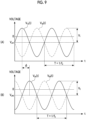
- Fig. 9 shows an example of a driving signal provided to the first actuator 21 and the second actuator 22.
- A) of Fig. 9 shows the driving voltage waveforms V 1A (t) and V 1B (t) included in the first driving signal.
- B) of Fig. 9 shows the driving voltage waveforms V 2A (t) and V 2B (t) included in the second driving signal.
- V 1A (t) and V 1B (t) are represented as follows, respectively.
- V 1 A t V off 1 + V 1 sin 2 ⁇ f d t
- V 1 B t V off 1 + V 1 sin 2 ⁇ f d t + ⁇
- V 1 is the amplitude voltage.
- V off1 is the bias voltage.
- f d is the driving frequency.
- t is time.
- the mirror portion 20 swings around the first axis a 1 (see Fig. 7 ).
- V 2A (t) and V 2B (t) are represented as follows, respectively.
- V 2 A t V off 2 + V 2 sin 2 ⁇ f d t + ⁇
- V 2 B t V off 2 + V 2 sin 2 ⁇ f d t + ⁇ + ⁇
- V 2 is the amplitude voltage.
- V off2 is the bias voltage.
- f d is the driving frequency.
- t is time.
- ⁇ is the phase difference between the driving voltage waveforms V 1A (t) and V 1B (t) and the driving voltage waveforms V 2A (t) and V 2B (t).
- ⁇ 90° is set in order to cause the mirror portion 20 to perform precession.
- the bias voltages V off1 and V off2 are DC voltages for determining a state where the mirror portion 20 is stationary.
- a plane including the reflecting surface 20A may not be parallel to an upper surface of the fixed portion 26 and may be inclined with respect to the upper surface of the fixed portion 26.
- the mirror portion 20 swings around the second axis a 2 (see Fig. 8 ).
- the first driving signal and the second driving signal have the same driving frequency f d and a phase difference of 90°.
- the meaning of "match” includes not only the meaning of perfect match but also the meaning of substantial match including allowable errors in design and manufacturing.
- Fig. 11 shows the precession of the mirror portion 20.
- the precession is a motion in which the normal line N of the reflecting surface 20A of the mirror portion 20 is deflected such that a circle is drawn about a rotation axis C parallel to the Z direction.
- the surface to be scanned 6 can be scanned with the light beam La such that a circle is drawn on the surface to be scanned 6.
- Fig. 12 shows an example of a configuration of the angle detection unit 5.
- the angle detection unit 5 comprises a light source 60, a light deflector 61, a position detector 62, a first optical system 63, and a second optical system 64.
- the light source 60 emits the light beam Lb for angle detection.
- the light source 60 is a laser diode that emits laser light having a wavelength of about 980 nm as the light beam Lb.
- the light deflector 61 has a cut surface formed by cutting a base material of a cylinder obliquely with respect to a rotational symmetry axis of the cylinder, and a reflecting surface 61A is formed on the cut surface.
- the light deflector 61 has a cut surface formed by cutting the base material of the cylinder in a plane forming an angle of 45° with respect to the rotational symmetry axis of the cylinder.
- the reflecting surface 61A is a surface mirror formed by depositing a metal thin film, such as gold (Au), aluminum (Al), or silver (Au), on the cut surface.
- the reflecting surface 61A may be a surface mirror formed by depositing a dielectric multi-layer film on the cut surface.
- the light deflector 61 is disposed such that the light beam Lb emitted from the light source 60 is incident at an incidence angle of about 45°.
- the light deflector 61 is an optical deflector that deflects the light beam Lb.
- the first optical system 63 is provided on an optical path of the light beam Lb between the light source 60 and the light deflector 61.
- the first optical system 63 condenses the light beam Lb emitted from the light source 60 and guides the condensed light beam to the reflecting surface 61A of the light deflector 61.
- the first optical system 63 is, for example, a biconvex lens, and is disposed such that an optical axis A1 thereof passes through the center of the optical path of the light beam Lb.
- the optical axis A1 is parallel to the X direction.
- An angle of the light beam Lb incident on the reflecting surface 61A is deflected by 90° and travels in the Z direction. That is, the light deflector 61 deflects the light beam Lb by 90°.
- the first optical system 63 is not an essential configuration in the technology of the present disclosure.
- the MMD 2 is disposed such that the light beam Lb deflected by the light deflector 61 is incident on a back surface 20B of the mirror portion 20.
- the back surface 20B is a surface opposite to the surface of the mirror portion 20 on which the reflecting surface 20A is formed.
- the back surface 20B of the mirror portion 20 is a surface that reflects the light beam Lb (that is, it is not a light absorption surface).
- the second optical system 64 is provided on an optical path of the light beam Lb between the light deflector 61 and the MMD 2.
- the second optical system 64 condenses the light beam Lb deflected by the light deflector 61 and guides the condensed light beam to the back surface 20B of the mirror portion 20.
- the second optical system 64 is, for example, a biconvex lens, and is disposed such that an optical axis A2 thereof passes through the center of the optical path of the light beam Lb reflected from the reflecting surface 61A. In the present embodiment, the optical axis A2 is parallel to the Z direction.
- the second optical system 64 is an example of an "optical system" according to the technology of the present disclosure.
- the light beams Lb deflected by the light deflector 61 are condensed by the second optical system 64 and guided to the back surface 20B of the mirror portion 20, at least a part of the light beams Lb deflected by the light deflector 61 need only be guided to the back surface 20B.
- the light beam Lb incident on the back surface 20B of the mirror portion 20 is reflected at a reflection angle corresponding to the deflection angle (first deflection angle ⁇ 1 and second deflection angle ⁇ 2 ) of the mirror portion 20. That is, the back surface 20B of the mirror portion 20 deflects the incident light beam Lb.
- the light beam Lb deflected by the back surface 20B of the mirror portion 20 is incident into the second optical system 64, and is guided to a light-receiving surface 62C of the position detector 62 by the second optical system 64.
- the second optical system 64 is configured such that the light beam Lb deflected by the back surface 20B of the mirror portion 20 is always incident on the light-receiving surface 62C of the position detector 62.
- the light beam Lb deflected by the back surface 20B of the mirror portion 20 is incident into a peripheral edge portion of the second optical system 64.
- the second optical system 64 condenses the incident light beam Lb and causes the condensed light beam to be incident into the position detector 62.
- a beam diameter D1 of the light beam Lb on the back surface 20B of the mirror portion 20 is larger than a beam diameter D2 of the light beam Lb on the light-receiving surface 62C of the position detector 62. That is, a relationship of D1 > D2 is satisfied.
- the position detector 62 includes a two-dimensional position sensitive detector (PSD) element 62A and a protective glass 62B disposed on the light-receiving surface 62C of the two-dimensional PSD element 62A.
- PSD position sensitive detector
- the position detector 62 is disposed such that the optical axis A2 of the second optical system 64 is orthogonal to the light-receiving surface 62C.
- the above-described light deflector 61 is disposed on the protective glass 62B in the center of the position detector 62. That is, a bottom surface of the light deflector 61 is joined to a surface of the protective glass 62B.
- the two-dimensional PSD element 62A detects the position of the light beam Lb incident on the light-receiving surface 62C.
- the two-dimensional PSD element 62A is a sensor capable of detecting a light quantity centroid position of a spot of the light beam Lb incident on the light-receiving surface 62C, and detects two-dimensional coordinates of the light quantity centroid position.
- the two-dimensional coordinates of the light quantity centroid position of the light beam Lb correspond to the deflection angles (first deflection angle ⁇ 1 and second deflection angle ⁇ 2 ) of the mirror portion 20.
- the position detector 62 outputs the detected two-dimensional coordinates to the driving control unit 4 as the above-described angle detection signal.
- Fig. 13 is a schematic perspective view of the position detector 62 and the light deflector 61.
- the two-dimensional PSD element 62A and the protective glass 62B constituting the position detector 62 each have a flat plate shape and a rectangular outer shape.
- Fig. 14 shows an example of a trajectory of the light beam Lb incident on the light-receiving surface 62C of the position detector 62.
- S indicates a spot of the light beam Lb.
- G indicates the light quantity centroid position of the light quantity of the spot S.
- TR indicates the trajectory of the light quantity centroid position.
- D indicates a shadow of the light deflector 61 reflected on the light-receiving surface 62C.
- the trajectory TR is substantially circular. Since the light deflector 61 is disposed in the center of the position detector 62, the trajectory TR orbits around the shadow D of the light deflector 61 and does not intersect the shadow D. Therefore, the position detector 62 accurately detects the two-dimensional coordinates of the light beam Lb incident on the light-receiving surface 62C.
- the light beam Lb can be made incident on the back surface 20B of the mirror portion 20 without using a beam splitter, and the light beam Lb deflected by the back surface 20B can be detected without being blocked by the light deflector 61.
- the efficiency and accuracy of the angle detection of the mirror portion 20 are improved as compared with the related art.
- the driving control unit 4 causes the mirror portion 20 to perform the precession, which is a motion in which the normal line N of the reflecting surface 20A is deflected such that a circle is drawn about the rotation axis C (see Fig. 11 ).
- the mirror portion 20 is moved such that the normal line N of the reflecting surface 20A draws a spiral shape about the rotation axis C.
- this motion is referred to as spiral motion.
- the amplitude voltages V 1 and V 2 need only be decreased or increased at a constant rate with the passage of time t in the first driving signal and the second driving signal shown in Fig. 9 .
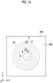
- Fig. 16 shows the trajectory of the light beam Lb incident on the light-receiving surface 62C of the position detector 62.
- the trajectory TR at the light quantity centroid position has a spiral shape.
- the trajectory TR orbits around the shadow D of the light deflector 61 and does not intersect with the shadow D. Therefore, the position detector 62 accurately detects the two-dimensional coordinates of the light beam Lb incident on the light-receiving surface 62C.
- the efficiency and accuracy of the angle detection of the mirror portion 20 are improved as compared with the related art.
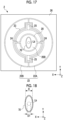
- Fig. 17 shows an example of a configuration on a back surface side of the MMD 2.
- an elliptical structure 70 may be provided on the back surface 20B of the mirror portion 20.
- the structure 70 is a so-called rib, and is formed by etching the above-described first silicon active layer 31.
- the structure 70 is disposed such that the center of the ellipse matches the center of the back surface 20B.
- a minor axis of the structure 70 is parallel to the X direction, and a major axis thereof is parallel to the Y direction.
- the light beam Lb deflected by the light deflector 61 is incident on the back surface 20B of the mirror portion 20 and is incident into an inner region of the structure 70 via the second optical system 64.
- the structure 70 has an elliptical shape, but the structure 70 is not limited to the elliptical shape, and may have an oval shape, a rectangular shape, or the like.
- the light source 60 included in the position detector 62 is provided separately from the light source 3 that irradiates the reflecting surface 20A of the mirror portion 20 with the light beam La
- the light source 60 and the light source 3 may be made common.
- a part of the light beam La emitted from the light source 3 may be made incident into the light deflector 61 as the light beam Lb for angle detection.
- the light deflector 61 since the light deflector 61 has the reflecting surface 61A that is the cut surface formed by cutting the base material of the cylinder obliquely with respect to the rotational symmetry axis of the cylinder, a shape of the reflecting surface 61A is the elliptical shape.
- the reflecting surface 61A is not limited to the elliptical shape, and may have a square shape, the rectangular shape, or other shapes. As shown in Fig. 19 as an example, the light deflector 61 may have the rectangular reflecting surface 61A formed by obliquely cutting a base material of a cube.
- the light deflector 61 may be an optical element such as a prism or the beam splitter. As shown in Fig. 20 as an example, the light deflector 61 may be a cube-type beam splitter.
- the cube-type beam splitter is configured by bonding slopes of two right-angle prisms to each other.
- An optical thin film is deposited on a bonding surface. The bonding surface constitutes the reflecting surface 61A.
- first actuator 21 and the second actuator 22 have an annular shape
- one or both of the first actuator 21 and the second actuator 22 may have a meander structure.
- a processing unit of the driving control unit 4 may be configured of one processor, or may be configured of a combination of two or more processors of the same type or different types (for example, a combination of a plurality of field programmable gate arrays (FPGAs) and/or a combination of a CPU and an FPGA).
- FPGAs field programmable gate arrays
Landscapes
- Physics & Mathematics (AREA)
- General Physics & Mathematics (AREA)
- Optics & Photonics (AREA)
- Engineering & Computer Science (AREA)
- Computer Networks & Wireless Communication (AREA)
- Radar, Positioning & Navigation (AREA)
- Remote Sensing (AREA)
- Computer Hardware Design (AREA)
- Microelectronics & Electronic Packaging (AREA)
- Mechanical Optical Scanning Systems (AREA)
- Mechanical Light Control Or Optical Switches (AREA)
Applications Claiming Priority (2)
| Application Number | Priority Date | Filing Date | Title |
|---|---|---|---|
| JP2021158222 | 2021-09-28 | ||
| PCT/JP2022/033041 WO2023053840A1 (ja) | 2021-09-28 | 2022-09-01 | 光走査装置 |
Publications (2)
| Publication Number | Publication Date |
|---|---|
| EP4411451A1 true EP4411451A1 (de) | 2024-08-07 |
| EP4411451A4 EP4411451A4 (de) | 2025-01-08 |
Family
ID=85780630
Family Applications (1)
| Application Number | Title | Priority Date | Filing Date |
|---|---|---|---|
| EP22875712.6A Withdrawn EP4411451A4 (de) | 2021-09-28 | 2022-09-01 | Optische abtastvorrichtung |
Country Status (5)
| Country | Link |
|---|---|
| US (1) | US20240219710A1 (de) |
| EP (1) | EP4411451A4 (de) |
| JP (1) | JPWO2023053840A1 (de) |
| CN (1) | CN118020011A (de) |
| WO (1) | WO2023053840A1 (de) |
Families Citing this family (1)
| Publication number | Priority date | Publication date | Assignee | Title |
|---|---|---|---|---|
| JP7481099B2 (ja) * | 2019-09-11 | 2024-05-10 | 浜松ホトニクス株式会社 | 光走査システムの製造方法、光走査装置の製造方法及びデータ取得方法 |
Family Cites Families (18)
| Publication number | Priority date | Publication date | Assignee | Title |
|---|---|---|---|---|
| FR2537732A1 (fr) * | 1982-12-10 | 1984-06-15 | Thomson Csf | Dispositif d'echauffement d'une zone annulaire superficielle d'un objet filiforme |
| JPH03288120A (ja) * | 1990-04-04 | 1991-12-18 | Ricoh Co Ltd | 走査光学装置 |
| JPH08288120A (ja) * | 1995-02-14 | 1996-11-01 | Toshiba Corp | 静磁界発生磁石及びmriシステム |
| JP2002148536A (ja) * | 2000-11-09 | 2002-05-22 | Olympus Optical Co Ltd | アクチュエータおよびその駆動方法 |
| US7295726B1 (en) * | 2003-12-02 | 2007-11-13 | Adriatic Research Institute | Gimbal-less micro-electro-mechanical-system tip-tilt and tip-tilt-piston actuators and a method for forming the same |
| JP2008116678A (ja) * | 2006-11-02 | 2008-05-22 | Sony Corp | 表示装置及び表示方法 |
| JP5510591B2 (ja) * | 2008-01-30 | 2014-06-04 | セイコーエプソン株式会社 | リフレクタ、光源装置及びプロジェクタ |
| JP5458827B2 (ja) * | 2009-11-25 | 2014-04-02 | 株式会社リコー | ビームピッチ調整方法、光走査装置および画像形成装置 |
| US20120236379A1 (en) * | 2010-08-23 | 2012-09-20 | Lighttime, Llc | Ladar using mems scanning |
| JP2012118125A (ja) * | 2010-11-29 | 2012-06-21 | Ricoh Co Ltd | 光走査装置及びその駆動方法。 |
| DE102011004477A1 (de) | 2011-02-21 | 2012-09-13 | Carl Zeiss Ag | Scanspiegelvorrichtung |
| US9213142B2 (en) * | 2013-11-21 | 2015-12-15 | Huawei Technologies Co., Ltd. | Device and method for micro-electro-mechanical-system photonic switch |
| JP2015141372A (ja) * | 2014-01-30 | 2015-08-03 | 株式会社ミツトヨ | 照射装置、照射方法、測定装置、及び測定方法 |
| JP6670143B2 (ja) * | 2016-03-24 | 2020-03-18 | パイオニア株式会社 | 揺動体装置の制御装置 |
| JP6924090B2 (ja) * | 2017-07-21 | 2021-08-25 | 浜松ホトニクス株式会社 | アクチュエータ装置 |
| JP7069629B2 (ja) * | 2017-10-13 | 2022-05-18 | 株式会社リコー | 距離測定装置、移動体、距離測定方法およびプログラム |
| WO2019176204A1 (ja) * | 2018-03-13 | 2019-09-19 | 三菱電機株式会社 | 光走査装置およびその制御方法 |
| DE102019204165A1 (de) * | 2019-03-26 | 2020-10-15 | Carl Zeiss Smt Gmbh | Optische anordnung und lithographieanlage |
-
2022
- 2022-09-01 JP JP2023550489A patent/JPWO2023053840A1/ja not_active Abandoned
- 2022-09-01 EP EP22875712.6A patent/EP4411451A4/de not_active Withdrawn
- 2022-09-01 CN CN202280064739.1A patent/CN118020011A/zh active Pending
- 2022-09-01 WO PCT/JP2022/033041 patent/WO2023053840A1/ja not_active Ceased
-
2024
- 2024-03-13 US US18/603,808 patent/US20240219710A1/en active Pending
Also Published As
| Publication number | Publication date |
|---|---|
| US20240219710A1 (en) | 2024-07-04 |
| EP4411451A4 (de) | 2025-01-08 |
| WO2023053840A1 (ja) | 2023-04-06 |
| JPWO2023053840A1 (de) | 2023-04-06 |
| CN118020011A (zh) | 2024-05-10 |
Similar Documents
| Publication | Publication Date | Title |
|---|---|---|
| EP4249985B1 (de) | Mikrospiegelvorrichtung und optische abtastvorrichtung | |
| US12339438B2 (en) | Micromirror device and optical scanning device | |
| US12436380B2 (en) | Optical scanning device and control method thereof | |
| US20240219710A1 (en) | Optical scanning device | |
| US12379588B2 (en) | Optical scanning device and method of driving micromirror device | |
| US12517346B2 (en) | Optical scanning device and method of driving micromirror device | |
| US12386172B2 (en) | Micromirror device and optical scanning device | |
| US20240036305A1 (en) | Image projection device and control method for image projection device | |
| US20250231398A1 (en) | Optical scanning device | |
| JP7794684B2 (ja) | 光走査装置及び異常検知方法 | |
| JP3114397B2 (ja) | 光学装置 | |
| JPH08254664A (ja) | 光学装置、光スキャン装置、加速度検出装置、圧力検出装置、及び画像検出装置 | |
| US20250208405A1 (en) | Micromirror device and optical scanning device | |
| US20250138163A1 (en) | Strain Sensors for Microelectromechanical System (MEMS) Devices | |
| US20250350699A1 (en) | Image drawing apparatus and driving method for image drawing apparatus | |
| JP7815020B2 (ja) | 光走査装置 | |
| JP7341782B2 (ja) | 角度検出装置 | |
| CN116134291A (zh) | 测距装置、测距方法及测距程序 | |
| CN121713109A (zh) | 反射镜装置及光扫描装置 | |
| JP2017138474A (ja) | ミラーユニット及び光走査装置 | |
| JP2008151640A (ja) | 計測装置 |
Legal Events
| Date | Code | Title | Description |
|---|---|---|---|
| STAA | Information on the status of an ep patent application or granted ep patent |
Free format text: STATUS: THE INTERNATIONAL PUBLICATION HAS BEEN MADE |
|
| PUAI | Public reference made under article 153(3) epc to a published international application that has entered the european phase |
Free format text: ORIGINAL CODE: 0009012 |
|
| STAA | Information on the status of an ep patent application or granted ep patent |
Free format text: STATUS: REQUEST FOR EXAMINATION WAS MADE |
|
| 17P | Request for examination filed |
Effective date: 20240229 |
|
| AK | Designated contracting states |
Kind code of ref document: A1 Designated state(s): AL AT BE BG CH CY CZ DE DK EE ES FI FR GB GR HR HU IE IS IT LI LT LU LV MC MK MT NL NO PL PT RO RS SE SI SK SM TR |
|
| DAV | Request for validation of the european patent (deleted) | ||
| DAX | Request for extension of the european patent (deleted) | ||
| A4 | Supplementary search report drawn up and despatched |
Effective date: 20241211 |
|
| RIC1 | Information provided on ipc code assigned before grant |
Ipc: G01S 17/00 20200101ALN20241205BHEP Ipc: G01S 7/481 20060101ALN20241205BHEP Ipc: G02B 26/08 20060101ALI20241205BHEP Ipc: B81B 3/00 20060101ALI20241205BHEP Ipc: G02B 26/10 20060101AFI20241205BHEP |
|
| STAA | Information on the status of an ep patent application or granted ep patent |
Free format text: STATUS: THE APPLICATION IS DEEMED TO BE WITHDRAWN |
|
| 18D | Application deemed to be withdrawn |
Effective date: 20250710 |