EP4407684A1 - Thin film transistor, display panel and preparation method therefor - Google Patents
Thin film transistor, display panel and preparation method therefor Download PDFInfo
- Publication number
- EP4407684A1 EP4407684A1 EP21801407.4A EP21801407A EP4407684A1 EP 4407684 A1 EP4407684 A1 EP 4407684A1 EP 21801407 A EP21801407 A EP 21801407A EP 4407684 A1 EP4407684 A1 EP 4407684A1
- Authority
- EP
- European Patent Office
- Prior art keywords
- electrode
- layer
- insulating layer
- active layer
- gate
- Prior art date
- Legal status (The legal status is an assumption and is not a legal conclusion. Google has not performed a legal analysis and makes no representation as to the accuracy of the status listed.)
- Pending
Links
Images


Classifications
-
- H—ELECTRICITY
- H10—SEMICONDUCTOR DEVICES; ELECTRIC SOLID-STATE DEVICES NOT OTHERWISE PROVIDED FOR
- H10D—INORGANIC ELECTRIC SEMICONDUCTOR DEVICES
- H10D30/00—Field-effect transistors [FET]
- H10D30/60—Insulated-gate field-effect transistors [IGFET]
- H10D30/67—Thin-film transistors [TFT]
- H10D30/6729—Thin-film transistors [TFT] characterised by the electrodes
- H10D30/673—Thin-film transistors [TFT] characterised by the electrodes characterised by the shapes, relative sizes or dispositions of the gate electrodes
- H10D30/6733—Multi-gate TFTs
- H10D30/6734—Multi-gate TFTs having gate electrodes arranged on both top and bottom sides of the channel, e.g. dual-gate TFTs
-
- G—PHYSICS
- G02—OPTICS
- G02F—OPTICAL DEVICES OR ARRANGEMENTS FOR THE CONTROL OF LIGHT BY MODIFICATION OF THE OPTICAL PROPERTIES OF THE MEDIA OF THE ELEMENTS INVOLVED THEREIN; NON-LINEAR OPTICS; FREQUENCY-CHANGING OF LIGHT; OPTICAL LOGIC ELEMENTS; OPTICAL ANALOGUE/DIGITAL CONVERTERS
- G02F1/00—Devices or arrangements for the control of the intensity, colour, phase, polarisation or direction of light arriving from an independent light source, e.g. switching, gating or modulating; Non-linear optics
- G02F1/01—Devices or arrangements for the control of the intensity, colour, phase, polarisation or direction of light arriving from an independent light source, e.g. switching, gating or modulating; Non-linear optics for the control of the intensity, phase, polarisation or colour
- G02F1/13—Devices or arrangements for the control of the intensity, colour, phase, polarisation or direction of light arriving from an independent light source, e.g. switching, gating or modulating; Non-linear optics for the control of the intensity, phase, polarisation or colour based on liquid crystals, e.g. single liquid crystal display cells
- G02F1/133—Constructional arrangements; Operation of liquid crystal cells; Circuit arrangements
- G02F1/136—Liquid crystal cells structurally associated with a semi-conducting layer or substrate, e.g. cells forming part of an integrated circuit
- G02F1/1362—Active matrix addressed cells
-
- G—PHYSICS
- G02—OPTICS
- G02F—OPTICAL DEVICES OR ARRANGEMENTS FOR THE CONTROL OF LIGHT BY MODIFICATION OF THE OPTICAL PROPERTIES OF THE MEDIA OF THE ELEMENTS INVOLVED THEREIN; NON-LINEAR OPTICS; FREQUENCY-CHANGING OF LIGHT; OPTICAL LOGIC ELEMENTS; OPTICAL ANALOGUE/DIGITAL CONVERTERS
- G02F1/00—Devices or arrangements for the control of the intensity, colour, phase, polarisation or direction of light arriving from an independent light source, e.g. switching, gating or modulating; Non-linear optics
- G02F1/01—Devices or arrangements for the control of the intensity, colour, phase, polarisation or direction of light arriving from an independent light source, e.g. switching, gating or modulating; Non-linear optics for the control of the intensity, phase, polarisation or colour
- G02F1/13—Devices or arrangements for the control of the intensity, colour, phase, polarisation or direction of light arriving from an independent light source, e.g. switching, gating or modulating; Non-linear optics for the control of the intensity, phase, polarisation or colour based on liquid crystals, e.g. single liquid crystal display cells
- G02F1/133—Constructional arrangements; Operation of liquid crystal cells; Circuit arrangements
- G02F1/136—Liquid crystal cells structurally associated with a semi-conducting layer or substrate, e.g. cells forming part of an integrated circuit
- G02F1/1362—Active matrix addressed cells
- G02F1/136231—Active matrix addressed cells for reducing the number of lithographic steps
-
- G—PHYSICS
- G02—OPTICS
- G02F—OPTICAL DEVICES OR ARRANGEMENTS FOR THE CONTROL OF LIGHT BY MODIFICATION OF THE OPTICAL PROPERTIES OF THE MEDIA OF THE ELEMENTS INVOLVED THEREIN; NON-LINEAR OPTICS; FREQUENCY-CHANGING OF LIGHT; OPTICAL LOGIC ELEMENTS; OPTICAL ANALOGUE/DIGITAL CONVERTERS
- G02F1/00—Devices or arrangements for the control of the intensity, colour, phase, polarisation or direction of light arriving from an independent light source, e.g. switching, gating or modulating; Non-linear optics
- G02F1/01—Devices or arrangements for the control of the intensity, colour, phase, polarisation or direction of light arriving from an independent light source, e.g. switching, gating or modulating; Non-linear optics for the control of the intensity, phase, polarisation or colour
- G02F1/13—Devices or arrangements for the control of the intensity, colour, phase, polarisation or direction of light arriving from an independent light source, e.g. switching, gating or modulating; Non-linear optics for the control of the intensity, phase, polarisation or colour based on liquid crystals, e.g. single liquid crystal display cells
- G02F1/133—Constructional arrangements; Operation of liquid crystal cells; Circuit arrangements
- G02F1/136—Liquid crystal cells structurally associated with a semi-conducting layer or substrate, e.g. cells forming part of an integrated circuit
- G02F1/1362—Active matrix addressed cells
- G02F1/136286—Wiring, e.g. gate line, drain line
-
- G—PHYSICS
- G02—OPTICS
- G02F—OPTICAL DEVICES OR ARRANGEMENTS FOR THE CONTROL OF LIGHT BY MODIFICATION OF THE OPTICAL PROPERTIES OF THE MEDIA OF THE ELEMENTS INVOLVED THEREIN; NON-LINEAR OPTICS; FREQUENCY-CHANGING OF LIGHT; OPTICAL LOGIC ELEMENTS; OPTICAL ANALOGUE/DIGITAL CONVERTERS
- G02F1/00—Devices or arrangements for the control of the intensity, colour, phase, polarisation or direction of light arriving from an independent light source, e.g. switching, gating or modulating; Non-linear optics
- G02F1/01—Devices or arrangements for the control of the intensity, colour, phase, polarisation or direction of light arriving from an independent light source, e.g. switching, gating or modulating; Non-linear optics for the control of the intensity, phase, polarisation or colour
- G02F1/13—Devices or arrangements for the control of the intensity, colour, phase, polarisation or direction of light arriving from an independent light source, e.g. switching, gating or modulating; Non-linear optics for the control of the intensity, phase, polarisation or colour based on liquid crystals, e.g. single liquid crystal display cells
- G02F1/133—Constructional arrangements; Operation of liquid crystal cells; Circuit arrangements
- G02F1/136—Liquid crystal cells structurally associated with a semi-conducting layer or substrate, e.g. cells forming part of an integrated circuit
- G02F1/1362—Active matrix addressed cells
- G02F1/1368—Active matrix addressed cells in which the switching element is a three-electrode device
-
- H—ELECTRICITY
- H10—SEMICONDUCTOR DEVICES; ELECTRIC SOLID-STATE DEVICES NOT OTHERWISE PROVIDED FOR
- H10D—INORGANIC ELECTRIC SEMICONDUCTOR DEVICES
- H10D30/00—Field-effect transistors [FET]
- H10D30/01—Manufacture or treatment
- H10D30/021—Manufacture or treatment of FETs having insulated gates [IGFET]
- H10D30/031—Manufacture or treatment of FETs having insulated gates [IGFET] of thin-film transistors [TFT]
- H10D30/0321—Manufacture or treatment of FETs having insulated gates [IGFET] of thin-film transistors [TFT] comprising silicon, e.g. amorphous silicon or polysilicon
-
- H—ELECTRICITY
- H10—SEMICONDUCTOR DEVICES; ELECTRIC SOLID-STATE DEVICES NOT OTHERWISE PROVIDED FOR
- H10D—INORGANIC ELECTRIC SEMICONDUCTOR DEVICES
- H10D30/00—Field-effect transistors [FET]
- H10D30/60—Insulated-gate field-effect transistors [IGFET]
- H10D30/67—Thin-film transistors [TFT]
- H10D30/6729—Thin-film transistors [TFT] characterised by the electrodes
-
- H—ELECTRICITY
- H10—SEMICONDUCTOR DEVICES; ELECTRIC SOLID-STATE DEVICES NOT OTHERWISE PROVIDED FOR
- H10D—INORGANIC ELECTRIC SEMICONDUCTOR DEVICES
- H10D30/00—Field-effect transistors [FET]
- H10D30/60—Insulated-gate field-effect transistors [IGFET]
- H10D30/67—Thin-film transistors [TFT]
- H10D30/674—Thin-film transistors [TFT] characterised by the active materials
- H10D30/6755—Oxide semiconductors, e.g. zinc oxide, copper aluminium oxide or cadmium stannate
-
- H—ELECTRICITY
- H10—SEMICONDUCTOR DEVICES; ELECTRIC SOLID-STATE DEVICES NOT OTHERWISE PROVIDED FOR
- H10D—INORGANIC ELECTRIC SEMICONDUCTOR DEVICES
- H10D86/00—Integrated devices formed in or on insulating or conducting substrates, e.g. formed in silicon-on-insulator [SOI] substrates or on stainless steel or glass substrates
- H10D86/01—Manufacture or treatment
- H10D86/021—Manufacture or treatment of multiple TFTs
-
- H—ELECTRICITY
- H10—SEMICONDUCTOR DEVICES; ELECTRIC SOLID-STATE DEVICES NOT OTHERWISE PROVIDED FOR
- H10D—INORGANIC ELECTRIC SEMICONDUCTOR DEVICES
- H10D86/00—Integrated devices formed in or on insulating or conducting substrates, e.g. formed in silicon-on-insulator [SOI] substrates or on stainless steel or glass substrates
- H10D86/40—Integrated devices formed in or on insulating or conducting substrates, e.g. formed in silicon-on-insulator [SOI] substrates or on stainless steel or glass substrates characterised by multiple TFTs
- H10D86/451—Integrated devices formed in or on insulating or conducting substrates, e.g. formed in silicon-on-insulator [SOI] substrates or on stainless steel or glass substrates characterised by multiple TFTs characterised by the compositions or shapes of the interlayer dielectrics
-
- H—ELECTRICITY
- H10—SEMICONDUCTOR DEVICES; ELECTRIC SOLID-STATE DEVICES NOT OTHERWISE PROVIDED FOR
- H10D—INORGANIC ELECTRIC SEMICONDUCTOR DEVICES
- H10D86/00—Integrated devices formed in or on insulating or conducting substrates, e.g. formed in silicon-on-insulator [SOI] substrates or on stainless steel or glass substrates
- H10D86/40—Integrated devices formed in or on insulating or conducting substrates, e.g. formed in silicon-on-insulator [SOI] substrates or on stainless steel or glass substrates characterised by multiple TFTs
- H10D86/441—Interconnections, e.g. scanning lines
-
- H—ELECTRICITY
- H10—SEMICONDUCTOR DEVICES; ELECTRIC SOLID-STATE DEVICES NOT OTHERWISE PROVIDED FOR
- H10D—INORGANIC ELECTRIC SEMICONDUCTOR DEVICES
- H10D86/00—Integrated devices formed in or on insulating or conducting substrates, e.g. formed in silicon-on-insulator [SOI] substrates or on stainless steel or glass substrates
- H10D86/40—Integrated devices formed in or on insulating or conducting substrates, e.g. formed in silicon-on-insulator [SOI] substrates or on stainless steel or glass substrates characterised by multiple TFTs
- H10D86/60—Integrated devices formed in or on insulating or conducting substrates, e.g. formed in silicon-on-insulator [SOI] substrates or on stainless steel or glass substrates characterised by multiple TFTs wherein the TFTs are in active matrices
Definitions
- the present disclosure relates to a field of display technologies, and more particularly, to a thin-film transistor (TFT), a display panel, and a manufacturing method of the display panel.
- TFT thin-film transistor
- a Vgs voltage needs to be reduced as much as possible. Specifically, this can be realized by reducing a thickness of a gate insulating layer.
- reducing the thickness of the gate insulating layer not only reduces a pressure resistance between a gate and a drain but also increases capacitance between the gate and a source/drain, affecting comprehensive electrical performance of the TFTs.
- Embodiments of the present disclosure provide a TFT, a display panel, and a manufacturing method of the display panel to effectively improve comprehensive electrical performance of TFTs.
- An embodiment of the present disclosure provides a TFT, comprising: a gate; a gate insulating layer disposed on a side of the gate; an active layer disposed on a side of the gate insulating layer away from the gate and disposed opposite to the gate; a first electrode disposed on a side of the active layer away from the gate; and an interlayer insulating layer disposed between the first electrode and the active layer to insulate the first electrode from the active layer, a first via penetrating the interlayer insulating layer and extending to a surface of the first electrode is defined on the interlayer insulating layer, the active layer is connected to the first electrode by the first via, and a thickness of the interlayer insulating layer is greater than a thickness of the gate insulating layer; and a second electrode connected to the active layer.
- the second electrode and the active layer are disposed on a same layer.
- the TFT further comprises: an auxiliary electrode disposed opposite to the active layer, wherein the interlayer insulating layer is disposed between the auxiliary electrode and the active layer.
- the first electrode and the auxiliary electrode are disposed on a same layer, and the active layer is connected to the first electrode by the first via.
- the active layer comprises a semiconductor part and a first electrode contact part, conductivity of the first electrode contact part is less than conductivity of the first electrode, and the conductivity of the first electrode contact part is greater than conductivity of the semiconductor part; and the first electrode contact part is connected to the first electrode by the first via.
- An embodiment of the present disclosure further provides a display panel, comprising: a first electrode disposed on a first metal layer; an interlayer insulating layer disposed on the first electrode, wherein a first via penetrating the interlayer insulating layer and extending to a surface of the first electrode is defined on the interlayer insulating layer; an active layer disposed on the interlayer insulating layer, wherein the active layer is connected to the first electrode by the first via; a second electrode connected to the active layer; a gate insulating layer disposed on the active layer; and a gate disposed on a second metal layer disposed on the gate insulating layer, wherein the gate is disposed opposite to the active layer.
- a thickness of the interlayer insulating layer is greater than a thickness of the gate insulating layer.
- the display panel further comprises: an auxiliary electrode disposed opposite to the active layer, wherein the interlayer insulating layer is disposed between the auxiliary electrode and the active layer.
- the first electrode is a drain and the second electrode is a source; and/or the first electrode is the source and the second electrode is the drain.
- the auxiliary electrode is disposed on the first metal layer, and the interlayer insulating layer covers the first electrode and the auxiliary electrode.
- the active layer comprises a semiconductor part and a first electrode contact part, conductivity of the first electrode contact part is less than conductivity of the first electrode, and the conductivity of the first electrode contact part is greater than conductivity of the semiconductor part; and the first electrode contact part is connected to the first electrode by the first via.
- the display panel further comprises a pixel electrode, wherein the pixel electrode and the active layer are disposed on a same layer, the pixel electrode is electrically connected to the active layer, and the active layer comprises a metal oxide semiconductor.
- the display panel further comprises: a substrate, wherein the first metal layer is disposed on the substrate and comprises a plurality of data lines; a plurality of scan lines disposed on the second metal layer, wherein the scan lines cross the data lines to define a plurality of sub-pixel units, and the gate, the second electrode, a thin-film transistor (TFT) composed of the first electrode, the second electrode, the first electrode, and the active layer and the pixel electrode connected to the TFT are disposed in the sub-pixel units; a passivation layer disposed on the second metal layer and covering the gate and the pixel electrode; and a common electrode disposed on the passivation layer and disposed opposite to the pixel electrode.
- TFT thin-film transistor
- a lateral edge of the gate, a lateral edge of the gate insulating layer, and a lateral edge of the semiconductor part of the active layer are aligned with each other.
- the thickness of the interlayer insulating layer is greater than or equal to two times the thickness of the gate insulating layer.
- the first metal layer further comprises a touch control signal line; and the display panel further comprises: a first touch control electrode, wherein the first touch control electrode and the active layer are disposed on a same layer, and the first touch control electrode is connected to the active layer; and a second touch control electrode, wherein the second touch control electrode is insulated from the first touch control electrode and is disposed opposite to the first touch control electrode.
- An embodiment of the present disclosure further provides a method of manufacturing the display panel, comprising following steps:
- a first electrode and a gate of a TFT are disposed on two sides of the active layer.
- a thickness of the gate insulating layer between the gate and the active layer and a thickness of the interlayer insulating layer between the first electrode and the active layer can be individually adjusted. Therefore, the thickness of the gate insulating layer can be reduced to reduce Vgs and the thickness of the interlayer insulating layer can be increased to improve a pressure resistance between the gate and the drain (first electrode).
- increasing the thickness of the interlayer insulating layer can also reduce capacitance between the gate and the drain (first electrode), thereby significantly improving comprehensive electrical performance of the TFT.
- the present disclosure provides a TFT, including a gate, a gate insulating layer, an active layer, an auxiliary electrode, an interlayer insulating layer, a first electrode, and a second electrode.
- the gate insulating layer is disposed on a side of the gate.
- the active layer is disposed on a side of the gate insulating layer away from the gate.
- the active layer is disposed opposite to the gate.
- the auxiliary electrode is disposed opposite to the active layer.
- the interlayer insulating layer is disposed between the auxiliary electrode and the active layer to insulate the auxiliary electrode from the active layer.
- a thickness of the interlayer insulating layer is greater than a thickness of the gate insulating layer.
- the first electrode and the auxiliary electrode are disposed on a same layer.
- a first via penetrating the interlayer insulating layer and extending to a surface of the first electrode is defined on the interlayer insulating layer.
- the active layer is connected to the first electrode by the first via.
- the second electrode is connected to the active layer.
- the second electrode and the active layer are disposed on a same layer.
- the TFT is disposed on a substrate 1.
- the substrate 1 is an array substrate.
- the substrate 1 is a rigid substrate which can be made of glass. It should be understood that the substrate 1 may also be a flexible substrate which can be made of an organic insulating material, such as polyimide (PI) and polyethylene terephthalate (PET), that can block moisture and oxygen. No specific limitation is given here.
- PI polyimide
- PET polyethylene terephthalate
- a first metal layer 2 is disposed on the substrate 1.
- the first metal layer 2 is patterned to form a first electrode 21 and an auxiliary electrode 22 of the TFT.
- the first metal layer 2 can be made of one or more of a common conductive metal, such as Mo, Al, Ti, and Cu, and an alloy.
- the first metal layer 2 may have a single-layer conductive layer structure made of single metal or may have a multi-layer conductive layer structure made of multiple metal. No specific limitation is given here.
- the first electrode 21 may be a source or a drain. In the present embodiment, the first electrode 21 is the drain connected to a data line.
- the interlayer insulating layer 3 is disposed on the first metal layer 2.
- the interlayer insulating layer 3 covers the first electrode 21 and the auxiliary electrode 22.
- a first via 31 penetrating the interlayer insulating layer 3 and extending to a surface of the first electrode 21 is defined on the interlayer insulating layer 3.
- the interlayer insulating layer 3 is formed by depositing or sputtering one or more of a common inorganic material, such as SiNx, SiOx, and Al 2 O 3 , that can block moisture and oxygen.
- the interlayer insulating layer 3 may also be made of an organic insulating layer to have a flat surface.
- the active layer 4 is disposed on the interlayer insulating layer 3.
- the active layer 4 may be made of a common semiconductor material such as a metal oxide, amorphous silicon, or polycrystalline silicon.
- a middle area of the active layer 4 corresponds to the auxiliary electrode 22.
- the active layer 4 includes a semiconductor part 41 and a first electrode contact part 42. Conductivity of the first electrode contact part 42 is less than conductivity of the first electrode 21. The conductivity of the first electrode contact part 42 is greater than conductivity of the semiconductor part 41.
- the first electrode contact part 42 is connected to the first electrode 21 by the first via 31.
- the second electrode 5 is connected to the active layer 4.
- the second electrode 5 is connected to the semiconductor part 41.
- the second electrode 5 may be the drain or the source.
- the second electrode 5 is the source connected to a pixel electrode or other circuits.
- the second electrode 5 and the active layer 4 are disposed on a same layer.
- the second electrode 5 and the first electrode contact part 42 are respectively disposed on two sides of the semiconductor part 41.
- the gate insulating layer 6 is disposed on the active layer 4.
- the gate insulating layer 6 covers the semiconductor part 41.
- the gate insulating layer 6 is formed by depositing or sputtering one or more of a common inorganic material such as SiNx, SiOx, and Al 2 O 3 .
- a common inorganic material such as SiNx, SiOx, and Al 2 O 3 .
- an insulating layer having a single layer can satisfy yield rate requirements of display panels.
- an insulating layer having a structure of multiple layers which are stacked may also be applied to improve a yield rate, thereby ensuring that moisture and oxygen can be effectively blocked.
- the gate insulating layer 6 has a structure having a single layer of SiO2 or a single layer of SiNx.
- the gate 71 is disposed on the gate insulating layer 6.
- the gate 71 is disposed opposite to the semiconductor part 41.
- the gate 71 can be made of one or more of a common conductive metal, such as Mo, Al, Ti, and Cu, and an alloy.
- the gate 71 may have a single-layer conducive layer structure having a single metal or may have a multi-layer conductive layer structure having multiple metals. A specific limitation is not given here.
- the auxiliary electrode 22 may be an auxiliary gate and/or a light-shielding electrode.
- the auxiliary electrode 22 is disposed opposite to the semiconductor part 41.
- the auxiliary electrode 22 may be made of a conductive material such as metal or indium tin oxide (ITO).
- ITO indium tin oxide
- the auxiliary electrode 22 can be the light-shielding electrode when it is made of metal or other non-transparent materials.
- the first electrode 21 and the gate 71 are disposed on two sides of the active layer 4.
- the first electrode 21 is insulated from the active layer 4 by the interlayer insulating layer 3.
- the gate 71 is insulated from the active layer 4 by the gate insulating layer 6.
- An insulating layer between the gate 71 and the active layer 4 is independent from an insulating layer between the source/drain and the active layer 4. Therefore, a thickness of the insulating layer between the gate 71 and the active layer 4 and a thickness of the insulating layer between the source/drain and the active layer 4 can be individually adjusted.
- a thickness of the interlayer insulating layer 3 is greater than a thickness of the gate insulating layer 6.
- the thickness of the gate insulating layer 6 is reduced according to a predetermined target value of Vgs of the TFT. Meanwhile, the thickness of the interlayer insulating layer 3 can be unchanged or increased. Therefore, a pressure resistance between the gate 71 and the drain (first electrode 21) will not be affected when the thickness of the gate insulating layer 6 is reduced, and capacitance between the gate 71 and the drain (first electrode 21) can be increased by appropriately increasing the thickness of the interlayer insulating layer 3. Because of the above design, every electrical performance of the TFT can be significantly improved.
- the thickness of the interlayer insulating layer 3 is greater than or equal to two times the thickness of the gate insulating layer 6.
- the thickness of the gate insulating layer 6 is one-third of the thickness of the interlayer insulating layer 3, comprehensive electrical performance of the TFT is improved.
- the active layer 4 includes a metal oxide semiconductor such as indium gallium zinc oxide (IGZO) or indium gallium zinc tin oxide (IGZTO).
- IGZO indium gallium zinc oxide
- IGZTO indium gallium zinc tin oxide
- the gate insulating layer 6 is patterned with the patterned gate 71 as a plate mask to expose the active layer 4 disposed on the first electrode 21.
- the exposed active layer 4 is metalized with the patterned gate 71 as a plate mask to form the second electrode 5 and the first electrode contact part 42 which are connected to the active layer 4.
- the first electrode contact part 42 is connected to the first electrode 21 by the first via 31. Patterning of the gate insulating layer 6 and metalization of the active layer 4 are completed by a self-alignment process of the gate 71. Therefore, two mask plates are saved, thereby reducing manufacturing cost.
- the present disclosure further provides a first embodiment of a display panel.
- the display panel includes a substrate 1, and a first metal layer 2, an interlayer insulating layer 3, an active layer 4, a second electrode 5, a gate insulating layer 6, a second metal layer 7, a pixel electrode 8, a passivation layer 9, and a common electrode layer 10 which are disposed on the substrate 1.
- the substrate 1 is an array substrate.
- the substrate 1 is a rigid substrate which can be made of glass. It should be understood that the substrate 1 may also be a flexible substrate which can be made of an organic insulating material, such as PI and PET, that can block moisture. No specific limitation is given here.
- a first metal layer 2 is disposed on the substrate 1.
- the first metal layer 2 is patterned to form a data line (not shown), and a first electrode 21, an auxiliary electrode 22, and a common electrode line 23 of the TFT.
- the first metal layer 2 can be made of one or more of a common conductive metal, such as Mo, Al, Ti, and Cu, and an alloy.
- the first metal layer 2 may have a single-layer conductive layer structure made of a single metal or may have a multi-layer conductive layer structure made of multiple metals. No specific limitation is given here.
- the first electrode 21 may be a source or a drain. In the present embodiment, the first electrode 21 is the drain connected to a data line.
- the auxiliary electrode 22 may be an auxiliary gate and/or a light-shielding electrode.
- the auxiliary electrode 22 is disposed opposite to the semiconductor part 41.
- the auxiliary electrode 22 may be made of a conductive material such as metal or ITO.
- the auxiliary electrode 22 can be the light-shielding electrode when it is made of metal or other non-transparent materials.
- the interlayer insulating layer 3 is disposed on the first metal layer 2.
- the interlayer insulating layer 3 covers the data line, the first electrode 21, the auxiliary electrode 22, and the common electrode line 23.
- a first via 31 penetrating the interlayer insulating layer 3 and extending to a surface of the first electrode 21 is defined on the interlayer insulating layer 3.
- the interlayer insulating layer 3 is formed by depositing or sputtering one or more of a common inorganic material, such as SiNx, SiOx, and Al 2 O 3 , that can block moisture and oxygen.
- a common inorganic material such as SiNx, SiOx, and Al 2 O 3
- an insulating layer having a structure of multiple layers which are stacked may also be applied to improve a yield rate, thereby ensuring that moisture and oxygen can be effectively blocked.
- the insulating layer 3 has a structure having a single layer of SiO2 or a single layer of SiNx.
- the active layer 4 is disposed on the interlayer insulating layer 3.
- the active layer 4 may be made of a common semiconductor material such as a metal oxide, an amorphous silicon, or a polycrystalline silicon.
- the active layer 4 is made of a metal oxide semiconductor.
- a middle area of the active layer 4 corresponds to the auxiliary electrode 22.
- the active layer 4 includes a semiconductor part 41 and a first electrode contact part 42. Conductivity of the first electrode contact part 42 is less than conductivity of the first electrode 21. The conductivity of the first electrode contact part 42 is greater than conductivity of the semiconductor part 41.
- the first electrode contact part 42 is connected to the first electrode 21 by the first via 31.
- the second electrode 5 is connected to the active layer 4.
- the second electrode 5 is connected to the semiconductor part 41.
- the second electrode 5 may be the drain or the source.
- the second electrode 5 and the active layer 4 are disposed on a same layer.
- the second electrode 5 and the first electrode contact part 42 are respectively disposed on two sides of the semiconductor part 41.
- the gate insulating layer 6 is disposed on the active layer 4.
- the gate insulating layer 6 covers the semiconductor part 41.
- the gate insulating layer 6 is formed by depositing or sputtering one or more of a common inorganic material such as SiNx, SiOx, and Al 2 O 3 .
- a common inorganic material such as SiNx, SiOx, and Al 2 O 3 .
- an insulating layer having a single layer can satisfy yield rate requirements of display panels.
- an insulating layer having a structure of multiple layers which are stacked may also be applied to improve a yield rate, thereby ensuring that moisture and oxygen can be effectively blocked.
- the gate insulating layer 6 has a structure having a single layer of SiO2 or a single layer of SiNx.
- the second metal layer 7 is disposed on the gate insulating layer 6.
- the second metal layer 7 is patterned to form a gate 71 and a scan line (not shown) of the TFT.
- the gate 71 is disposed opposite to the semiconductor part 41.
- the second metal layer 7 may be made of one or more of common conductive metal, such as Mo, Al, Ti, and Cu, and an alloy.
- the second metal layer 7 may have a single-layer conductive layer structure having a single metal or may be a multi-layer conductive metal structure having multiple metals. A specific limitation is not given here.
- the pixel electrode 8 is disposed on the interlayer insulating layer 3.
- the pixel electrode 8, the active layer 4, and the second electrode 5 are disposed on a same layer.
- the pixel electrode 8 and the second electrode 5 are formed by performing a metal-doping process on the active layer 4.
- the pixel electrode 8 and the second electrode 5 are integrated.
- An end of the second electrode 5 is connected to the semiconductor part 41, and another end of the second electrode 5 is connected to the pixel electrode 8.
- the pixel electrode 8 and the second electrode 5 are formed by performing the metal-doping process on an oxide semiconductor layer.
- the second electrode 5 can be omitted or can be regarded as a part of the pixel electrode 8, which can be determined according to the pattern of the pixel electrode 8.
- the passivation layer 9 is disposed on the second metal layer 7.
- the passivation layer 9 covers the gate 71, the scan line, the first electrode contact part 42, the second electrode 5, and the pixel electrode 8.
- a second via 91 penetrating the passivation layer 9 and the interlayer insulating layer 3 and extending to a surface of a common electrode line 23 is defined on the passivation layer 9.
- the passivation layer 9 is formed by depositing or sputtering one or more of a common inorganic material such as SiNx, SiOx, and Al 2 O 3 .
- an insulating layer having a single layer can satisfy yield rate requirements of display panels.
- an insulating layer having a structure of multiple layers which are stacked may also be applied to improve a yield rate, thereby ensuring that moisture and oxygen can be effectively blocked.
- the common electrode 10 is disposed on the passivation layer 9.
- the common electrode 10 can be made of a transparent ITO material.
- the common electrode 10 is connected to the common electrode line 23 by the second via 91.
- the display panel is a fringe field switching (FFS) display panel.
- FFS fringe field switching
- the interlayer insulating layer 3 below the pixel electrode 8 needs to be an organic insulating planarization layer. Therefore, the pixel electrode 8 can be ensured to be disposed on a same horizontal surface as possible.
- the common electrode 10 is disposed opposite to the pixel electrode 8, thereby generating a horizontal electrical afield to drive the liquid crystals. It should be understood that the common electrode 10 may have a star-shaped pattern, a comb-shaped pattern, or other patterns. A specific limitation is not given here.
- a first alignment (not shown) is disposed on the common electrode 10 to adjust an orientation angle of the liquid crystals.
- the display panel further includes a base plate 11, and a color filter layer 12, a light-shielding layer 13, and a second alignment layer (not shown) which are disposed on the substrate 11.
- the base plate 11 is disposed opposite to the substrate 1. A material of the base plate 11 and a material of the substrate 1 are same an are not described here.
- the color filter layer 12 includes a plurality of optical filters 121. Each sub-pixel area is provided with one optical filter 121.
- the optical filters 121 are disposed opposite to the pixel electrode 8.
- the light-shielding layer 13 is disposed between two adjacent optical filters 121 to prevent a mixture of colors.
- the light-shielding layer 13 is made of a black resin material.
- the second alignment layer covers the color filter layer 12 and the light-shielding layer 13 to adjust the orientation angle of the liquid crystals.
- the display panel further includes a liquid crystal layer (not shown) and a barrier component (not shown) disposed between the substrate 1 and the base plate 11.
- a display area of the display panel is provided with a plurality of scan lines extending along a first direction and a plurality of data lines extending along a second direction.
- the scan lines cross the data lines to define a plurality of sub-pixel areas arranged in an array manner.
- the TFT composed of the gate 71, the second electrode 5, the first electrode 21, and the active layer 4 and the pixel electrode 8 connected to the TFT are disposed in the sub-pixel units.
- the auxiliary electrode 22 is disposed opposite to the semiconductor part 41.
- the auxiliary electrode 22 may be made of a conductive material such as metal or ITO.
- the auxiliary electrode 22 can be the light-shielding electrode when it is made of metal or other non-transparent materials.
- the first electrode 21 and the gate 71 of the TFT are disposed on two sides of the active layer 4.
- the first electrode 21 is insulated from the active layer 4 by the interlayer insulating layer 3.
- the gate 71 is insulated from the active layer 4 by the gate insulating layer 6.
- An insulating layer between the gate 71 and the active layer 4 is independent from an insulating layer between the source/drain and the active layer 4. Therefore, a thickness of the insulating layer between the gate 71 and the active layer 4 and a thickness of the insulating layer between the source/drain and the active layer 4 can be individually adjusted.
- a thickness of the interlayer insulating layer 3 is greater than a thickness of the gate insulating layer 6.
- the thickness of the gate insulating layer 6 is reduced according to a predetermined target value of Vgs of the TFT. Meanwhile, the thickness of the interlayer insulating layer 3 can be unchanged or increased. Therefore, a pressure resistance between the gate 71 and the drain (first electrode 21) will not be affected when the thickness of the gate insulating layer 6 is reduced, and capacitance between the gate 71 and the drain (first electrode 21) can be increased by appropriately increasing the thickness of the interlayer insulating layer 3. Because of the above design, every electrical performance of the TFT can be significantly improved.
- the thickness of the interlayer insulating layer 3 is greater than or equal to two times the thickness of the gate insulating layer 6.
- the thickness of the gate insulating layer 6 is one-third of the thickness of the interlayer insulating layer 3, comprehensive electrical performance of the TFT is improved.
- the active layer 4 includes a metal oxide semiconductor such as IGZO or IGZTO.
- the gate insulating layer 6 is patterned with the patterned gate 71 as a plate mask to expose the active layer 4 disposed on the first electrode 21.
- the exposed active layer 4 is metalized with the patterned gate 71 as a plate mask to form the second electrode 5 and the first electrode contact part 42 which are connected to the active layer 4.
- the first electrode contact part 42 is connected to the first electrode 21 by the first via 31. Patterning of the gate insulating layer 6 and metalization of the active layer 4 are completed by a self-alignment process of the gate 71. Therefore, two mask plates are saved, thereby reducing manufacturing cost.
- the present embodiment further provides a second embodiment of a display panel. Differences between the present embodiment and the first embodiment include:
- the first metal layer 2 further includes a touch control signal line.
- the first metal layer 2 is patterned to form the first electrode 21, the auxiliary electrode 22, the common electrode line 23, and a touch control signal line 24.
- a third via 92 which penetrates the passivation layer 9 and the interlayer insulating layer 3, extends to the second via 91 on the surface of the common electrode line 23, and extends to a surface of the touch control signal line 24, is defined on the passivation layer 9.
- the display panel When the display panel has a mutual-capacitive touch control structure, the display panel further includes a first touch control electrode 14 and a second touch control electrode 15.
- the first touch control electrode 14 and the active layer 4 are disposed on a same layer.
- the touch control electrode 14 is connected to the active layer 4.
- the second touch control electrode 15 is insulated from the first touch control electrode 14 and is disposed opposite to the first touch control electrode 14.
- the second touch control electrode 15 and the common electrode 10 are disposed on a same layer.
- the second touch control electrode 15 is connected to the touch control signal line 24 by the third via 92.
- the display panel When the display panel has a self-capacitive touch control structure, the display panel only includes a layer of the second touch control electrode 15 disposed on a same layer as the common electrode.
- the second touch control electrode 15 is connected to the touch control signal line 24 by the third via 92.
- the present disclosure further provides a specific embodiment of a method of manufacturing a display panel, including following steps:
- the step B2 includes forming the first metal layer 2 on the substrate 1, and patterning the first metal layer 2 to form the first electrode 21, an auxiliary electrode layer 2, a common electrode line 23, and a data line (not shown).
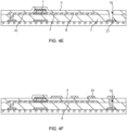
- FIG. 4B disposing an interlayer insulating layer 3 on the first metal layer 2, and patterning the interlayer insulating layer 3 to form a first via 31.
- the first via 31 penetrates the interlayer insulating layer 3 and extends to a surface of the first electrode 21.
- the active layer 4 is connected to the first electrode 21 by the first via 31.
- the active layer 4 is an oxide semiconductor layer.
- the gate 71 is disposed opposite to the auxiliary electrode 22.
- Using the gate 71 as a mask plate to pattern the gate insulating layer 6 can save one mask plate.
- the first electrode contact part 42 is connected to the first electrode 21 by the first via 31.
- the second electrode 5 is connected to the active layer 4.
- the second electrode 5 is connected to the semiconductor part 41.
- the second electrode 5 is a drain or a source.
- the second electrode 5 and the semiconductor part 41 are disposed on a same layer.
- the second electrode 5 and the first electrode contact part 42 are respectively disposed on two sides of the semiconductor part 41.
- the second electrode 5 and the pixel electrode 8 have a same material.
- a pattern of the pixel electrode 8 is planar.
- the second electrode 5 and the pixel electrode 8 are integrated.
- the pixel electrode 8 and the second electrode 5 are formed by performing a metal-doping process on an oxide semiconductor layer.
- the second electrode 5 can be omitted or can be regarded as a part of the pixel electrode 8, which can be determined according to the pattern of the pixel electrode 8.
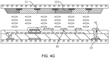
- a passivation layer 9 on the second metal layer 7, wherein the passivation layer 9 covers the gate 71, the scan line, the first electrode contact part 42, the second electrode 5, and the pixel electrode 8, and patterning the passivation layer 9 to define a second via 91 penetrating the passivation layer 9 and the interlayer insulating layer 3 and extending to a surface of a common electrode line 23.
- the common electrode 10 can be made of a transparent ITO material.
- the common electrode 10 is comb-shaped. By stacking the planarly-disposed pixel electrode 8 and the patterned common electrode 10, a horizontal edge electrical field can be generated, thereby driving liquid crystals to be oriented.
- the common electrode 10 is connected to the common electrode line 23 by the second via 91.
- the first electrode 21 and the gate 71 of the TFT are disposed on two sides of the active layer 4.
- the gate insulating layer 6 between the gate 71 and the active layer 4 is independent from the interlayer insulating layer 6 between the first electrode 21 and the active layer 4. Therefore, a thickness of the gate insulating layer 6 between the gate 71 and the active layer 4 and a thickness of the interlayer insulating layer 6 between the first electrode 21 and the active layer 4 can be individually adjusted. Therefore, the thickness of the gate insulating layer 6 can be reduced to reduce Vgs and the thickness of the interlayer insulating layer 3 can be increased to improve a pressure resistance between the gate 7 and the drain (first electrode 21). Moreover, increasing the thickness of the interlayer insulating layer 3 can also reduce capacitance between the gate 7 and the drain (first electrode 21), thereby significantly improving comprehensive electrical performance of the TFT.
Landscapes
- Physics & Mathematics (AREA)
- Nonlinear Science (AREA)
- Engineering & Computer Science (AREA)
- Microelectronics & Electronic Packaging (AREA)
- Mathematical Physics (AREA)
- Chemical & Material Sciences (AREA)
- Crystallography & Structural Chemistry (AREA)
- General Physics & Mathematics (AREA)
- Optics & Photonics (AREA)
- Devices For Indicating Variable Information By Combining Individual Elements (AREA)
- Liquid Crystal (AREA)
- Thin Film Transistor (AREA)
Abstract
Description
- The present disclosure relates to a field of display technologies, and more particularly, to a thin-film transistor (TFT), a display panel, and a manufacturing method of the display panel.
- In conventional back-channel etched (BCE) TFTs, to improve electrical performance, a Vgs voltage needs to be reduced as much as possible. Specifically, this can be realized by reducing a thickness of a gate insulating layer. However, reducing the thickness of the gate insulating layer not only reduces a pressure resistance between a gate and a drain but also increases capacitance between the gate and a source/drain, affecting comprehensive electrical performance of the TFTs.
- Embodiments of the present disclosure provide a TFT, a display panel, and a manufacturing method of the display panel to effectively improve comprehensive electrical performance of TFTs.
- An embodiment of the present disclosure provides a TFT, comprising: a gate; a gate insulating layer disposed on a side of the gate; an active layer disposed on a side of the gate insulating layer away from the gate and disposed opposite to the gate; a first electrode disposed on a side of the active layer away from the gate; and an interlayer insulating layer disposed between the first electrode and the active layer to insulate the first electrode from the active layer, a first via penetrating the interlayer insulating layer and extending to a surface of the first electrode is defined on the interlayer insulating layer, the active layer is connected to the first electrode by the first via, and a thickness of the interlayer insulating layer is greater than a thickness of the gate insulating layer; and a second electrode connected to the active layer. The second electrode and the active layer are disposed on a same layer.
- Optionally, in some specific embodiments of the present disclosure, the TFT further comprises: an auxiliary electrode disposed opposite to the active layer, wherein the interlayer insulating layer is disposed between the auxiliary electrode and the active layer.
- Optionally, in some specific embodiments of the present disclosure, the first electrode and the auxiliary electrode are disposed on a same layer, and the active layer is connected to the first electrode by the first via.
- Optionally, in some specific embodiments of the present disclosure, the active layer comprises a semiconductor part and a first electrode contact part, conductivity of the first electrode contact part is less than conductivity of the first electrode, and the conductivity of the first electrode contact part is greater than conductivity of the semiconductor part; and the first electrode contact part is connected to the first electrode by the first via.
- An embodiment of the present disclosure further provides a display panel, comprising: a first electrode disposed on a first metal layer; an interlayer insulating layer disposed on the first electrode, wherein a first via penetrating the interlayer insulating layer and extending to a surface of the first electrode is defined on the interlayer insulating layer; an active layer disposed on the interlayer insulating layer, wherein the active layer is connected to the first electrode by the first via; a second electrode connected to the active layer; a gate insulating layer disposed on the active layer; and a gate disposed on a second metal layer disposed on the gate insulating layer, wherein the gate is disposed opposite to the active layer. A thickness of the interlayer insulating layer is greater than a thickness of the gate insulating layer.
- Optionally, in some specific embodiments of the present disclosure, the display panel further comprises: an auxiliary electrode disposed opposite to the active layer, wherein the interlayer insulating layer is disposed between the auxiliary electrode and the active layer. The first electrode is a drain and the second electrode is a source; and/or the first electrode is the source and the second electrode is the drain.
- Optionally, in some specific embodiments of the present disclosure, the auxiliary electrode is disposed on the first metal layer, and the interlayer insulating layer covers the first electrode and the auxiliary electrode.
- Optionally, in some specific embodiments of the present disclosure, the active layer comprises a semiconductor part and a first electrode contact part, conductivity of the first electrode contact part is less than conductivity of the first electrode, and the conductivity of the first electrode contact part is greater than conductivity of the semiconductor part; and the first electrode contact part is connected to the first electrode by the first via.
- Optionally, in some specific embodiments of the present disclosure, the display panel further comprises a pixel electrode, wherein the pixel electrode and the active layer are disposed on a same layer, the pixel electrode is electrically connected to the active layer, and the active layer comprises a metal oxide semiconductor.
- Optionally, in some specific embodiments of the present disclosure, the display panel further comprises: a substrate, wherein the first metal layer is disposed on the substrate and comprises a plurality of data lines; a plurality of scan lines disposed on the second metal layer, wherein the scan lines cross the data lines to define a plurality of sub-pixel units, and the gate, the second electrode, a thin-film transistor (TFT) composed of the first electrode, the second electrode, the first electrode, and the active layer and the pixel electrode connected to the TFT are disposed in the sub-pixel units; a passivation layer disposed on the second metal layer and covering the gate and the pixel electrode; and a common electrode disposed on the passivation layer and disposed opposite to the pixel electrode.
- Optionally, in some specific embodiments of the present disclosure, a lateral edge of the gate, a lateral edge of the gate insulating layer, and a lateral edge of the semiconductor part of the active layer are aligned with each other.
- Optionally, in some specific embodiments of the present disclosure, the thickness of the interlayer insulating layer is greater than or equal to two times the thickness of the gate insulating layer.
- Optionally, in some specific embodiments of the present disclosure, the first metal layer further comprises a touch control signal line; and the display panel further comprises: a first touch control electrode, wherein the first touch control electrode and the active layer are disposed on a same layer, and the first touch control electrode is connected to the active layer; and a second touch control electrode, wherein the second touch control electrode is insulated from the first touch control electrode and is disposed opposite to the first touch control electrode.
- An embodiment of the present disclosure further provides a method of manufacturing the display panel, comprising following steps:
- B1, providing a substrate;
- B2, forming a first metal layer on the substrate, and patterning the first metal layer to form a first electrode;
- B3, disposing an interlayer insulating layer on the first metal layer, and patterning the interlayer insulating layer to form a first via;
- B4, disposing a patterned active layer on the interlayer insulating layer, wherein the active layer is connected to the first electrode by the first via, and the active layer comprises a metal oxide semiconductor;
- B5, forming a gate insulating layer and a second metal layer on the active layer, and a thickness of the interlayer insulating layer is greater than or equal to two times a thickness of the gate insulating layer; patterning the second metal layer to form a gate, wherein the gate and the active layer are opposite to each other; using the patterned gate as a mask plate to pattern the gate insulating layer to expose the active layer disposed on the first electrode; and using the patterned gate as the mask plate to metalize the exposed active layer to form a second electrode and a first electrode contact part which are connected to the active layer, wherein the first electrode contact part is connected to the first electrode by the first via.
- Regarding the beneficial effects: in the present disclosure, a first electrode and a gate of a TFT are disposed on two sides of the active layer. By individually disposing a gate insulating layer between the gate and the active layer and an interlayer insulating layer between the first electrode and the active layer, a thickness of the gate insulating layer between the gate and the active layer and a thickness of the interlayer insulating layer between the first electrode and the active layer can be individually adjusted. Therefore, the thickness of the gate insulating layer can be reduced to reduce Vgs and the thickness of the interlayer insulating layer can be increased to improve a pressure resistance between the gate and the drain (first electrode). Moreover, increasing the thickness of the interlayer insulating layer can also reduce capacitance between the gate and the drain (first electrode), thereby significantly improving comprehensive electrical performance of the TFT.
- In addition, in a manufacturing method of a display panel provided by the present disclosure, patterning of a gate insulating layer and metalization of an active layer are completed by a gate self-alignment process of a gate. Therefore, two mask plates can be saved, thereby reducing manufacturing cost.
- The accompanying figures to be used in the description of embodiments of the present disclosure or prior art will be described in brief to more clearly illustrate the technical solutions of the embodiments or the prior art. The accompanying figures described below are only part of the embodiments of the present disclosure, from which those skilled in the art can derive further figures without making any inventive efforts.
-
FIG. 1 is a cross-sectional schematic view showing a TFT according to a specific embodiment of the present disclosure. -
FIG. 2 is a cross-sectional schematic view showing a display area of a display panel according to a first embodiment of the present disclosure. -
FIG. 3 is a cross-sectional schematic view showing a display area of a display panel according to a second embodiment of the present disclosure. -
FIGs. 4A to 4G are structural schematic views showing manufacturing processes of the display panel inFIG. 2 . - Hereinafter preferred embodiments of the present disclosure will be described with reference to the accompanying drawings to exemplify the embodiments of the present disclosure can be implemented, which can fully describe the technical contents of the present disclosure to make the technical content of the present disclosure clearer and easy to understand. However, the described embodiments are only some of the embodiments of the present disclosure, but not all of the embodiments. All other embodiments obtained by those skilled in the art based on the embodiments of the present disclosure without creative efforts are within the scope of the present disclosure.
- The present disclosure provides a TFT, including a gate, a gate insulating layer, an active layer, an auxiliary electrode, an interlayer insulating layer, a first electrode, and a second electrode. The gate insulating layer is disposed on a side of the gate. The active layer is disposed on a side of the gate insulating layer away from the gate. The active layer is disposed opposite to the gate. The auxiliary electrode is disposed opposite to the active layer. The interlayer insulating layer is disposed between the auxiliary electrode and the active layer to insulate the auxiliary electrode from the active layer. A thickness of the interlayer insulating layer is greater than a thickness of the gate insulating layer. The first electrode and the auxiliary electrode are disposed on a same layer. A first via penetrating the interlayer insulating layer and extending to a surface of the first electrode is defined on the interlayer insulating layer. The active layer is connected to the first electrode by the first via. The second electrode is connected to the active layer. The second electrode and the active layer are disposed on a same layer.
- Specifically, as shown in
FIG. 1 , The TFT is disposed on asubstrate 1. - The
substrate 1 is an array substrate. Thesubstrate 1 is a rigid substrate which can be made of glass. It should be understood that thesubstrate 1 may also be a flexible substrate which can be made of an organic insulating material, such as polyimide (PI) and polyethylene terephthalate (PET), that can block moisture and oxygen. No specific limitation is given here. - A
first metal layer 2 is disposed on thesubstrate 1. Thefirst metal layer 2 is patterned to form afirst electrode 21 and anauxiliary electrode 22 of the TFT. Thefirst metal layer 2 can be made of one or more of a common conductive metal, such as Mo, Al, Ti, and Cu, and an alloy. Thefirst metal layer 2 may have a single-layer conductive layer structure made of single metal or may have a multi-layer conductive layer structure made of multiple metal. No specific limitation is given here. Thefirst electrode 21 may be a source or a drain. In the present embodiment, thefirst electrode 21 is the drain connected to a data line. - The interlayer insulating
layer 3 is disposed on thefirst metal layer 2. The interlayer insulatinglayer 3 covers thefirst electrode 21 and theauxiliary electrode 22. A first via 31 penetrating theinterlayer insulating layer 3 and extending to a surface of thefirst electrode 21 is defined on theinterlayer insulating layer 3. Commonly, theinterlayer insulating layer 3 is formed by depositing or sputtering one or more of a common inorganic material, such as SiNx, SiOx, and Al2O3, that can block moisture and oxygen. The interlayer insulatinglayer 3 may also be made of an organic insulating layer to have a flat surface. - The
active layer 4 is disposed on theinterlayer insulating layer 3. Theactive layer 4 may be made of a common semiconductor material such as a metal oxide, amorphous silicon, or polycrystalline silicon. A middle area of theactive layer 4 corresponds to theauxiliary electrode 22. Theactive layer 4 includes asemiconductor part 41 and a firstelectrode contact part 42. Conductivity of the firstelectrode contact part 42 is less than conductivity of thefirst electrode 21. The conductivity of the firstelectrode contact part 42 is greater than conductivity of thesemiconductor part 41. The firstelectrode contact part 42 is connected to thefirst electrode 21 by the first via 31. - The
second electrode 5 is connected to theactive layer 4. Thesecond electrode 5 is connected to thesemiconductor part 41. Thesecond electrode 5 may be the drain or the source. In the present embodiment, thesecond electrode 5 is the source connected to a pixel electrode or other circuits. Thesecond electrode 5 and theactive layer 4 are disposed on a same layer. Thesecond electrode 5 and the firstelectrode contact part 42 are respectively disposed on two sides of thesemiconductor part 41. - The
gate insulating layer 6 is disposed on theactive layer 4. Thegate insulating layer 6 covers thesemiconductor part 41. Commonly, thegate insulating layer 6 is formed by depositing or sputtering one or more of a common inorganic material such as SiNx, SiOx, and Al2O3. Generally, an insulating layer having a single layer can satisfy yield rate requirements of display panels. However, in display panels having an active layer made of polysilicon or a metal oxide, an insulating layer having a structure of multiple layers which are stacked may also be applied to improve a yield rate, thereby ensuring that moisture and oxygen can be effectively blocked. In the present embodiment, thegate insulating layer 6 has a structure having a single layer of SiO2 or a single layer of SiNx. - The
gate 71 is disposed on thegate insulating layer 6. Thegate 71 is disposed opposite to thesemiconductor part 41. Thegate 71 can be made of one or more of a common conductive metal, such as Mo, Al, Ti, and Cu, and an alloy. Thegate 71 may have a single-layer conducive layer structure having a single metal or may have a multi-layer conductive layer structure having multiple metals. A specific limitation is not given here. - The
auxiliary electrode 22 may be an auxiliary gate and/or a light-shielding electrode. Theauxiliary electrode 22 is disposed opposite to thesemiconductor part 41. When theauxiliary electrode 22 is the auxiliary gate, theauxiliary electrode 22 may be made of a conductive material such as metal or indium tin oxide (ITO). By disposing theauxiliary electrode 22 opposite to thesemiconductor part 41, electrical performance of the TFT can be effectively improved. Theauxiliary electrode 22 can be the light-shielding electrode when it is made of metal or other non-transparent materials. By disposing theauxiliary electrode 22 opposite to thesemiconductor part 41, light can be prevented from being emitted on thesemiconductor part 41, which affects electrical performance of the TFT. - In the TFT provided by the present embodiment, the
first electrode 21 and thegate 71 are disposed on two sides of theactive layer 4. Thefirst electrode 21 is insulated from theactive layer 4 by theinterlayer insulating layer 3. Thegate 71 is insulated from theactive layer 4 by thegate insulating layer 6. An insulating layer between thegate 71 and theactive layer 4 is independent from an insulating layer between the source/drain and theactive layer 4. Therefore, a thickness of the insulating layer between thegate 71 and theactive layer 4 and a thickness of the insulating layer between the source/drain and theactive layer 4 can be individually adjusted. As such, an issue of conventional technologies can be solved: when a gate and a source/drain are disposed on a same side of an active layer, reducing a thickness of a gate insulating layer to reduce Vgs will simultaneously reduce other electrical performance of TFTs. - A thickness of the interlayer insulating
layer 3 is greater than a thickness of thegate insulating layer 6. The thickness of thegate insulating layer 6 is reduced according to a predetermined target value of Vgs of the TFT. Meanwhile, the thickness of the interlayer insulatinglayer 3 can be unchanged or increased. Therefore, a pressure resistance between thegate 71 and the drain (first electrode 21) will not be affected when the thickness of thegate insulating layer 6 is reduced, and capacitance between thegate 71 and the drain (first electrode 21) can be increased by appropriately increasing the thickness of the interlayer insulatinglayer 3. Because of the above design, every electrical performance of the TFT can be significantly improved. - Optionally, the thickness of the interlayer insulating
layer 3 is greater than or equal to two times the thickness of thegate insulating layer 6. When the thickness of thegate insulating layer 6 is one-third of the thickness of the interlayer insulatinglayer 3, comprehensive electrical performance of the TFT is improved. - Optionally, a lateral edge of the
gate 71, a lateral edge of thegate insulating layer 6, and a lateral edge of thesemiconductor part 41 of theactive layer 4 are aligned with each other, thereby reducing a number of mask plates for manufacturing the TFT. Specifically, theactive layer 4 includes a metal oxide semiconductor such as indium gallium zinc oxide (IGZO) or indium gallium zinc tin oxide (IGZTO). Thegate insulating layer 6 is patterned with the patternedgate 71 as a plate mask to expose theactive layer 4 disposed on thefirst electrode 21. The exposedactive layer 4 is metalized with the patternedgate 71 as a plate mask to form thesecond electrode 5 and the firstelectrode contact part 42 which are connected to theactive layer 4. The firstelectrode contact part 42 is connected to thefirst electrode 21 by the first via 31. Patterning of thegate insulating layer 6 and metalization of theactive layer 4 are completed by a self-alignment process of thegate 71. Therefore, two mask plates are saved, thereby reducing manufacturing cost. - As shown in
FIG 2 , the present disclosure further provides a first embodiment of a display panel. The display panel includes asubstrate 1, and afirst metal layer 2, aninterlayer insulating layer 3, anactive layer 4, asecond electrode 5, agate insulating layer 6, asecond metal layer 7, apixel electrode 8, apassivation layer 9, and acommon electrode layer 10 which are disposed on thesubstrate 1. - The
substrate 1 is an array substrate. Thesubstrate 1 is a rigid substrate which can be made of glass. It should be understood that thesubstrate 1 may also be a flexible substrate which can be made of an organic insulating material, such as PI and PET, that can block moisture. No specific limitation is given here. - A
first metal layer 2 is disposed on thesubstrate 1. Thefirst metal layer 2 is patterned to form a data line (not shown), and afirst electrode 21, anauxiliary electrode 22, and acommon electrode line 23 of the TFT. Thefirst metal layer 2 can be made of one or more of a common conductive metal, such as Mo, Al, Ti, and Cu, and an alloy. Thefirst metal layer 2 may have a single-layer conductive layer structure made of a single metal or may have a multi-layer conductive layer structure made of multiple metals. No specific limitation is given here. Thefirst electrode 21 may be a source or a drain. In the present embodiment, thefirst electrode 21 is the drain connected to a data line. - The
auxiliary electrode 22 may be an auxiliary gate and/or a light-shielding electrode. Theauxiliary electrode 22 is disposed opposite to thesemiconductor part 41. When theauxiliary electrode 22 is the auxiliary gate, theauxiliary electrode 22 may be made of a conductive material such as metal or ITO. By disposing theauxiliary electrode 22 opposite to thesemiconductor part 41, electrical performance of the TFT can be effectively improved. Theauxiliary electrode 22 can be the light-shielding electrode when it is made of metal or other non-transparent materials. By disposing theauxiliary electrode 22 opposite to thesemiconductor part 41, light can be prevented from being emitted on thesemiconductor part 41, and electrical performance of the TFT can be prevented from being affected. - The interlayer insulating
layer 3 is disposed on thefirst metal layer 2. The interlayer insulatinglayer 3 covers the data line, thefirst electrode 21, theauxiliary electrode 22, and thecommon electrode line 23. A first via 31 penetrating theinterlayer insulating layer 3 and extending to a surface of thefirst electrode 21 is defined on theinterlayer insulating layer 3. Commonly, theinterlayer insulating layer 3 is formed by depositing or sputtering one or more of a common inorganic material, such as SiNx, SiOx, and Al2O3, that can block moisture and oxygen. Generally, an insulating layer having a single layer can satisfy yield rate requirements of display panels. However, in display panels having an active layer made of polysilicon or a metal oxide, an insulating layer having a structure of multiple layers which are stacked may also be applied to improve a yield rate, thereby ensuring that moisture and oxygen can be effectively blocked. In the present embodiment, the insulatinglayer 3 has a structure having a single layer of SiO2 or a single layer of SiNx. - The
active layer 4 is disposed on theinterlayer insulating layer 3. Theactive layer 4 may be made of a common semiconductor material such as a metal oxide, an amorphous silicon, or a polycrystalline silicon. In the present embodiment, theactive layer 4 is made of a metal oxide semiconductor. A middle area of theactive layer 4 corresponds to theauxiliary electrode 22. Theactive layer 4 includes asemiconductor part 41 and a firstelectrode contact part 42. Conductivity of the firstelectrode contact part 42 is less than conductivity of thefirst electrode 21. The conductivity of the firstelectrode contact part 42 is greater than conductivity of thesemiconductor part 41. The firstelectrode contact part 42 is connected to thefirst electrode 21 by the first via 31. - The
second electrode 5 is connected to theactive layer 4. Thesecond electrode 5 is connected to thesemiconductor part 41. Thesecond electrode 5 may be the drain or the source. Thesecond electrode 5 and theactive layer 4 are disposed on a same layer. Thesecond electrode 5 and the firstelectrode contact part 42 are respectively disposed on two sides of thesemiconductor part 41. - The
gate insulating layer 6 is disposed on theactive layer 4. Thegate insulating layer 6 covers thesemiconductor part 41. Commonly, thegate insulating layer 6 is formed by depositing or sputtering one or more of a common inorganic material such as SiNx, SiOx, and Al2O3. Generally, an insulating layer having a single layer can satisfy yield rate requirements of display panels. However, in display panels having an active layer made of polysilicon or a metal oxide, an insulating layer having a structure of multiple layers which are stacked may also be applied to improve a yield rate, thereby ensuring that moisture and oxygen can be effectively blocked. In the present embodiment, thegate insulating layer 6 has a structure having a single layer of SiO2 or a single layer of SiNx. - The
second metal layer 7 is disposed on thegate insulating layer 6. Thesecond metal layer 7 is patterned to form agate 71 and a scan line (not shown) of the TFT. Thegate 71 is disposed opposite to thesemiconductor part 41. Thesecond metal layer 7 may be made of one or more of common conductive metal, such as Mo, Al, Ti, and Cu, and an alloy. Thesecond metal layer 7 may have a single-layer conductive layer structure having a single metal or may be a multi-layer conductive metal structure having multiple metals. A specific limitation is not given here. - The
pixel electrode 8 is disposed on theinterlayer insulating layer 3. Thepixel electrode 8, theactive layer 4, and thesecond electrode 5 are disposed on a same layer. Thepixel electrode 8 and thesecond electrode 5 are formed by performing a metal-doping process on theactive layer 4. Thepixel electrode 8 and thesecond electrode 5 are integrated. An end of thesecond electrode 5 is connected to thesemiconductor part 41, and another end of thesecond electrode 5 is connected to thepixel electrode 8. Thepixel electrode 8 and thesecond electrode 5 are formed by performing the metal-doping process on an oxide semiconductor layer. In some embodiments, thesecond electrode 5 can be omitted or can be regarded as a part of thepixel electrode 8, which can be determined according to the pattern of thepixel electrode 8. - The
passivation layer 9 is disposed on thesecond metal layer 7. Thepassivation layer 9 covers thegate 71, the scan line, the firstelectrode contact part 42, thesecond electrode 5, and thepixel electrode 8. A second via 91 penetrating thepassivation layer 9 and the interlayer insulatinglayer 3 and extending to a surface of acommon electrode line 23 is defined on thepassivation layer 9. Commonly, thepassivation layer 9 is formed by depositing or sputtering one or more of a common inorganic material such as SiNx, SiOx, and Al2O3. Generally, an insulating layer having a single layer can satisfy yield rate requirements of display panels. However, in display panels having an active layer made of polysilicon or a metal oxide, an insulating layer having a structure of multiple layers which are stacked may also be applied to improve a yield rate, thereby ensuring that moisture and oxygen can be effectively blocked. - The
common electrode 10 is disposed on thepassivation layer 9. Thecommon electrode 10 can be made of a transparent ITO material. Thecommon electrode 10 is connected to thecommon electrode line 23 by the second via 91. In the present embodiment, the display panel is a fringe field switching (FFS) display panel. By stacking the planarly-disposedpixel electrode 8 and the patternedcommon electrode 10, a horizontal edge electrical field can be generated, thereby driving liquid crystals to be oriented. To ensure display quality, theinterlayer insulating layer 3 below thepixel electrode 8 needs to be an organic insulating planarization layer. Therefore, thepixel electrode 8 can be ensured to be disposed on a same horizontal surface as possible. Thecommon electrode 10 is disposed opposite to thepixel electrode 8, thereby generating a horizontal electrical afield to drive the liquid crystals. It should be understood that thecommon electrode 10 may have a star-shaped pattern, a comb-shaped pattern, or other patterns. A specific limitation is not given here. - A first alignment (not shown) is disposed on the
common electrode 10 to adjust an orientation angle of the liquid crystals. - The display panel further includes a
base plate 11, and acolor filter layer 12, a light-shielding layer 13, and a second alignment layer (not shown) which are disposed on thesubstrate 11. - The
base plate 11 is disposed opposite to thesubstrate 1. A material of thebase plate 11 and a material of thesubstrate 1 are same an are not described here. - The
color filter layer 12 includes a plurality ofoptical filters 121. Each sub-pixel area is provided with oneoptical filter 121. Theoptical filters 121 are disposed opposite to thepixel electrode 8. - The light-
shielding layer 13 is disposed between two adjacentoptical filters 121 to prevent a mixture of colors. Generally, the light-shielding layer 13 is made of a black resin material. - The second alignment layer covers the
color filter layer 12 and the light-shielding layer 13 to adjust the orientation angle of the liquid crystals. - The display panel further includes a liquid crystal layer (not shown) and a barrier component (not shown) disposed between the
substrate 1 and thebase plate 11. - A display area of the display panel is provided with a plurality of scan lines extending along a first direction and a plurality of data lines extending along a second direction. The scan lines cross the data lines to define a plurality of sub-pixel areas arranged in an array manner. The TFT composed of the
gate 71, thesecond electrode 5, thefirst electrode 21, and theactive layer 4 and thepixel electrode 8 connected to the TFT are disposed in the sub-pixel units. - The
auxiliary electrode 22 is disposed opposite to thesemiconductor part 41. When theauxiliary electrode 22 is the auxiliary gate, theauxiliary electrode 22 may be made of a conductive material such as metal or ITO. By disposing theauxiliary electrode 22 opposite to thesemiconductor part 41, electrical performance of the TFT can be effectively improved. Theauxiliary electrode 22 can be the light-shielding electrode when it is made of metal or other non-transparent materials. By disposing theauxiliary electrode 22 opposite to thesemiconductor part 41, light can be prevented from being emitted on thesemiconductor part 41, and electrical performance of the TFT can be prevented from being affected. - In the display panel provided by the present embodiment, the
first electrode 21 and thegate 71 of the TFT are disposed on two sides of theactive layer 4. Thefirst electrode 21 is insulated from theactive layer 4 by theinterlayer insulating layer 3. Thegate 71 is insulated from theactive layer 4 by thegate insulating layer 6. An insulating layer between thegate 71 and theactive layer 4 is independent from an insulating layer between the source/drain and theactive layer 4. Therefore, a thickness of the insulating layer between thegate 71 and theactive layer 4 and a thickness of the insulating layer between the source/drain and theactive layer 4 can be individually adjusted. As such, an issue of conventional technologies can be solved: when a gate and a source/drain are disposed on a same side of an active layer, reducing a thickness of a gate insulating layer to reduce Vgs will simultaneously reduce other electrical performance of TFTs. - A thickness of the interlayer insulating
layer 3 is greater than a thickness of thegate insulating layer 6. The thickness of thegate insulating layer 6 is reduced according to a predetermined target value of Vgs of the TFT. Meanwhile, the thickness of the interlayer insulatinglayer 3 can be unchanged or increased. Therefore, a pressure resistance between thegate 71 and the drain (first electrode 21) will not be affected when the thickness of thegate insulating layer 6 is reduced, and capacitance between thegate 71 and the drain (first electrode 21) can be increased by appropriately increasing the thickness of the interlayer insulatinglayer 3. Because of the above design, every electrical performance of the TFT can be significantly improved. - Optionally, the thickness of the interlayer insulating
layer 3 is greater than or equal to two times the thickness of thegate insulating layer 6. When the thickness of thegate insulating layer 6 is one-third of the thickness of the interlayer insulatinglayer 3, comprehensive electrical performance of the TFT is improved. - Optionally, a lateral edge of the
gate 71, a lateral edge of thegate insulating layer 6, and a lateral edge of thesemiconductor part 41 of theactive layer 4 are aligned with each other, thereby reducing a number of mask plates for manufacturing the TFT. Specifically, theactive layer 4 includes a metal oxide semiconductor such as IGZO or IGZTO. Thegate insulating layer 6 is patterned with the patternedgate 71 as a plate mask to expose theactive layer 4 disposed on thefirst electrode 21. The exposedactive layer 4 is metalized with the patternedgate 71 as a plate mask to form thesecond electrode 5 and the firstelectrode contact part 42 which are connected to theactive layer 4. The firstelectrode contact part 42 is connected to thefirst electrode 21 by the first via 31. Patterning of thegate insulating layer 6 and metalization of theactive layer 4 are completed by a self-alignment process of thegate 71. Therefore, two mask plates are saved, thereby reducing manufacturing cost. - As shown in
FIG. 3 , the present embodiment further provides a second embodiment of a display panel. Differences between the present embodiment and the first embodiment include: - The
first metal layer 2 further includes a touch control signal line. Thefirst metal layer 2 is patterned to form thefirst electrode 21, theauxiliary electrode 22, thecommon electrode line 23, and a touchcontrol signal line 24. - A third via 92, which penetrates the
passivation layer 9 and the interlayer insulatinglayer 3, extends to the second via 91 on the surface of thecommon electrode line 23, and extends to a surface of the touchcontrol signal line 24, is defined on thepassivation layer 9. - When the display panel has a mutual-capacitive touch control structure, the display panel further includes a first
touch control electrode 14 and a secondtouch control electrode 15. The firsttouch control electrode 14 and theactive layer 4 are disposed on a same layer. Thetouch control electrode 14 is connected to theactive layer 4. The secondtouch control electrode 15 is insulated from the firsttouch control electrode 14 and is disposed opposite to the firsttouch control electrode 14. The secondtouch control electrode 15 and thecommon electrode 10 are disposed on a same layer. The secondtouch control electrode 15 is connected to the touchcontrol signal line 24 by the third via 92. - When the display panel has a self-capacitive touch control structure, the display panel only includes a layer of the second
touch control electrode 15 disposed on a same layer as the common electrode. The secondtouch control electrode 15 is connected to the touchcontrol signal line 24 by the third via 92. - Other structures of the present embodiment are same as the structures of the first embodiment and are not described again here.
- As shown in
FIGs. 4A to 4G , the present disclosure further provides a specific embodiment of a method of manufacturing a display panel, including following steps: - B1, providing a
substrate 1. - B2, as shown in
FIG. 4A , forming afirst metal layer 2 on thesubstrate 1, and patterning thefirst metal layer 2 to form afirst electrode 21. - Optionally, the step B2 includes forming the
first metal layer 2 on thesubstrate 1, and patterning thefirst metal layer 2 to form thefirst electrode 21, anauxiliary electrode layer 2, acommon electrode line 23, and a data line (not shown). - B3, as shown in
FIG. 4B , disposing aninterlayer insulating layer 3 on thefirst metal layer 2, and patterning theinterlayer insulating layer 3 to form a first via 31. The first via 31 penetrates the interlayer insulatinglayer 3 and extends to a surface of thefirst electrode 21. - B4, as shown in
FIG. 4C , disposing a patternedactive layer 4 on theinterlayer insulating layer 3. Theactive layer 4 is connected to thefirst electrode 21 by the first via 31. Theactive layer 4 is an oxide semiconductor layer. - B5, as shown in
FIG. 4D , forming agate insulating layer 6 and asecond metal layer 7 on theactive layer 4, wherein a thickness of the interlayer insulatinglayer 3 is greater than or equal to two times a thickness of thegate insulating layer 6, and patterning thesecond metal layer 7 to form agate 71 and a scan line (not shown), wherein thegate 71 is disposed opposite to theactive layer 4. Optionally, thegate 71 is disposed opposite to theauxiliary electrode 22. - Patterning the
gate insulating layer 6 with the patternedgate 71 as a mask plate to expose theactive layer 4 disposed on thefirst electrode 21, aligning a lateral edge of thegate 71 with a lateral edge of thegate insulating layer 6. Using thegate 71 as a mask plate to pattern thegate insulating layer 6 can save one mask plate. - Performing a metal-doping process on the exposed
active layer 4 with the patternedgate 71 as a mask plate to form apixel electrode 8, and asecond electrode 5 and the firstelectrode contact part 42 which are connected to asemiconductor part 41, and aligning the lateral edge of thegate 71, the lateral edge of thegate insulating layer 6, and a lateral edge of thesemiconductor part 41 with each other. The firstelectrode contact part 42 is connected to thefirst electrode 21 by the first via 31. - The
second electrode 5 is connected to theactive layer 4. Thesecond electrode 5 is connected to thesemiconductor part 41. Thesecond electrode 5 is a drain or a source. Thesecond electrode 5 and thesemiconductor part 41 are disposed on a same layer. Thesecond electrode 5 and the firstelectrode contact part 42 are respectively disposed on two sides of thesemiconductor part 41. - The
second electrode 5 and thepixel electrode 8 have a same material. A pattern of thepixel electrode 8 is planar. Thesecond electrode 5 and thepixel electrode 8 are integrated. Thepixel electrode 8 and thesecond electrode 5 are formed by performing a metal-doping process on an oxide semiconductor layer. In some embodiments, thesecond electrode 5 can be omitted or can be regarded as a part of thepixel electrode 8, which can be determined according to the pattern of thepixel electrode 8. - B6, as shown in
FIG. 4E , forming apassivation layer 9 on thesecond metal layer 7, wherein thepassivation layer 9 covers thegate 71, the scan line, the firstelectrode contact part 42, thesecond electrode 5, and thepixel electrode 8, and patterning thepassivation layer 9 to define a second via 91 penetrating thepassivation layer 9 and the interlayer insulatinglayer 3 and extending to a surface of acommon electrode line 23. - B7, as shown in
FIG. 4F , forming a common electrode layer on thepassivation layer 9, and patterning the common electrode layer to form acommon electrode 10. Thecommon electrode 10 can be made of a transparent ITO material. Thecommon electrode 10 is comb-shaped. By stacking the planarly-disposedpixel electrode 8 and the patternedcommon electrode 10, a horizontal edge electrical field can be generated, thereby driving liquid crystals to be oriented. Thecommon electrode 10 is connected to thecommon electrode line 23 by the second via 91. - B8, as shown in
FIG. 4G , covering a color filter substrate on thecommon electrode 10, and sealing the liquid crystals between the color filter substrate and anoptical filter 121. - In the display panel provided by the present embodiment, the
first electrode 21 and thegate 71 of the TFT are disposed on two sides of theactive layer 4. Thegate insulating layer 6 between thegate 71 and theactive layer 4 is independent from the interlayer insulatinglayer 6 between thefirst electrode 21 and theactive layer 4. Therefore, a thickness of thegate insulating layer 6 between thegate 71 and theactive layer 4 and a thickness of the interlayer insulatinglayer 6 between thefirst electrode 21 and theactive layer 4 can be individually adjusted. Therefore, the thickness of thegate insulating layer 6 can be reduced to reduce Vgs and the thickness of the interlayer insulatinglayer 3 can be increased to improve a pressure resistance between thegate 7 and the drain (first electrode 21). Moreover, increasing the thickness of the interlayer insulatinglayer 3 can also reduce capacitance between thegate 7 and the drain (first electrode 21), thereby significantly improving comprehensive electrical performance of the TFT. - In addition, in a manufacturing method of a display panel provided by the present disclosure, patterning of the
gate insulating layer 6 and metalization of anactive layer 4 are completed by a gate self-alignment process of thegate 71. Therefore, two mask plates can be saved, thereby reducing manufacturing cost. - A TFT, a display panel, and a manufacturing method of the display panel have been described in detail by the above embodiments, which illustrate principles and implementations thereof. However, the description of the above embodiments is only for helping to understand the technical solution of the present disclosure and core ideas thereof, and it is understood by those skilled in the art that many changes and modifications to the described embodiments can be carried out without departing from the scope and the spirit of the disclosure that is intended to be limited only by the appended claims.
Claims (20)
- A thin-film transistor (TFT), comprising:a gate;a gate insulating layer disposed on a side of the gate;an active layer disposed on a side of the gate insulating layer away from the gate and disposed opposite to the gate;a first electrode disposed on a side of the active layer away from the gate; andan interlayer insulating layer disposed between the first electrode and the active layer to insulate the first electrode from the active layer, a first via penetrating the interlayer insulating layer and extending to a surface of the first electrode is defined on the interlayer insulating layer, the active layer is connected to the first electrode by the first via, and a thickness of the interlayer insulating layer is greater than a thickness of the gate insulating layer; anda second electrode connected to the active layer, wherein the second electrode and the active layer are disposed on a same layer.
- The TFT of claim 1, comprising:
an auxiliary electrode disposed opposite to the active layer, wherein the interlayer insulating layer is disposed between the auxiliary electrode and the active layer. - The TFT of claim 2, wherein the first electrode and the auxiliary electrode are disposed on a same layer, and the active layer is connected to the first electrode by the first via.
- The TFT of claim 1, wherein the active layer comprises a semiconductor part and a first electrode contact part, conductivity of the first electrode contact part is less than conductivity of the first electrode, and the conductivity of the first electrode contact part is greater than conductivity of the semiconductor part; and
the first electrode contact part is connected to the first electrode by the first via. - The TFT of claim 4, wherein a lateral edge of the gate, a lateral edge of the gate insulating layer, and a lateral edge of the semiconductor part of the active layer are aligned with each other.
- The TFT of claim 1, wherein the thickness of the interlayer insulating layer is greater than or equal to two times the thickness of the gate insulating layer.
- The TFT of claim 6, wherein the thickness of the interlayer insulating layer is equal to three times the thickness of the gate insulating layer.
- A display panel, comprising:a first electrode disposed on a first metal layer;an interlayer insulating layer disposed on the first electrode, wherein a first via penetrating the interlayer insulating layer and extending to a surface of the first electrode is defined on the interlayer insulating layer;an active layer disposed on the interlayer insulating layer, wherein the active layer is connected to the first electrode by the first via;a second electrode connected to the active layer;a gate insulating layer disposed on the active layer; anda gate disposed on a second metal layer disposed on the gate insulating layer, wherein the gate is disposed opposite to the active layer;wherein a thickness of the interlayer insulating layer is greater than a thickness of the gate insulating layer.
- The display panel of claim 8, comprising:
an auxiliary electrode disposed opposite to the active layer, wherein the interlayer insulating layer is disposed between the auxiliary electrode and the active layer. - The display panel of claim 8, wherein the first electrode is a drain and the second electrode is a source; and/or
the first electrode is the source and the second electrode is the drain. - The display panel of claim 9, wherein the auxiliary electrode is disposed on the first metal layer, and the interlayer insulating layer covers the first electrode and the auxiliary electrode.
- The display panel of claim 8, wherein the active layer comprises a semiconductor part and a first electrode contact part, conductivity of the first electrode contact part is less than conductivity of the first electrode, and the conductivity of the first electrode contact part is greater than conductivity of the semiconductor part; and
the first electrode contact part is connected to the first electrode by the first via. - The display panel of claim 8, comprising a pixel electrode, wherein the pixel electrode and the active layer are disposed on a same layer, the pixel electrode is electrically connected to the active layer, and the active layer comprises a metal oxide semiconductor.
- The display panel of claim 13, comprising:a substrate, wherein the first metal layer is disposed on the substrate and comprises a plurality of data lines;a plurality of scan lines disposed on the second metal layer, wherein the scan lines cross the data lines to define a plurality of sub-pixel units, and the gate, the second electrode, a thin-film transistor (TFT) composed of the first electrode, the second electrode, the first electrode, and the active layer and the pixel electrode connected to the TFT are disposed in the sub-pixel units;a passivation layer disposed on the second metal layer and covering the gate and the pixel electrode; anda common electrode disposed on the passivation layer and disposed opposite to the pixel electrode.
- The display panel of claim 8, wherein a lateral edge of the gate, a lateral edge of the gate insulating layer, and a lateral edge of the semiconductor part of the active layer are aligned with each other.
- The display panel of claim 8, wherein the thickness of the interlayer insulating layer is greater than or equal to two times the thickness of the gate insulating layer.
- The display panel of claim 16, wherein the thickness of the interlayer insulating layer is equal to three times the thickness of the gate insulating layer.
- The display panel of claim 8, wherein the first metal layer comprises a touch control signal line; and
the display panel comprises:
a first touch control electrode, wherein the first touch control electrode and the active layer are disposed on a same layer, and the first touch control electrode is connected to the active layer. - The display panel of claim 8, comprising a second touch control electrode, wherein the second touch control electrode is insulated from the first touch control electrode and is disposed opposite to the first touch control electrode.
- A method of manufacturing the display panel, comprising following steps:B1, providing a substrate;B2, forming a first metal layer on the substrate, and patterning the first metal layer to form a first electrode;B3, disposing an interlayer insulating layer on the first metal layer, and patterning the interlayer insulating layer to form a first via;B4, disposing a patterned active layer on the interlayer insulating layer, wherein the active layer is connected to the first electrode by the first via, and the active layer comprises a metal oxide semiconductor;B5, forming a gate insulating layer and a second metal layer on the active layer, and a thickness of the interlayer insulating layer is greater than or equal to two times a thickness of the gate insulating layer;patterning the second metal layer to form a gate, wherein the gate and the active layer are disposed opposite to each other;using the patterned gate as a mask plate to pattern the gate insulating layer to expose the active layer disposed on the first electrode; andusing the patterned gate as the mask plate to metalize the exposed active layer to form a second electrode and a first electrode contact part which are connected to the active layer, wherein the first electrode contact part is connected to the first electrode by the first via.
Applications Claiming Priority (2)
| Application Number | Priority Date | Filing Date | Title |
|---|---|---|---|
| CN202111120728.4A CN113871401B (en) | 2021-09-24 | 2021-09-24 | Thin film transistor, display panel and method for manufacturing the same |
| PCT/CN2021/121819 WO2023044950A1 (en) | 2021-09-24 | 2021-09-29 | Thin film transistor, display panel and preparation method therefor |
Publications (2)
| Publication Number | Publication Date |
|---|---|
| EP4407684A1 true EP4407684A1 (en) | 2024-07-31 |
| EP4407684A4 EP4407684A4 (en) | 2025-08-06 |
Family
ID=78993743
Family Applications (1)
| Application Number | Title | Priority Date | Filing Date |
|---|---|---|---|
| EP21801407.4A Pending EP4407684A4 (en) | 2021-09-24 | 2021-09-29 | Thin-film transistor, display panel and manufacturing method therefor |
Country Status (5)
| Country | Link |
|---|---|
| US (1) | US20240047537A1 (en) |
| EP (1) | EP4407684A4 (en) |
| JP (1) | JP7816983B2 (en) |
| CN (1) | CN113871401B (en) |
| WO (1) | WO2023044950A1 (en) |
Families Citing this family (6)
| Publication number | Priority date | Publication date | Assignee | Title |
|---|---|---|---|---|
| CN114447090A (en) * | 2022-02-10 | 2022-05-06 | 京东方科技集团股份有限公司 | Display substrate and display device |
| CN114721553B (en) * | 2022-06-06 | 2022-12-13 | 惠科股份有限公司 | Touch structure, OLED touch display panel and manufacturing method |
| CN115241208A (en) | 2022-07-08 | 2022-10-25 | 武汉华星光电技术有限公司 | display panel |
| CN115458587B (en) * | 2022-09-19 | 2025-10-28 | 武汉华星光电技术有限公司 | Display panel |
| CN115483277A (en) * | 2022-09-30 | 2022-12-16 | 惠科股份有限公司 | Thin film transistor, display panel and manufacturing method thereof |
| CN116224664B (en) * | 2023-01-30 | 2025-07-25 | 惠科股份有限公司 | Gamma debugging method and array substrate |
Family Cites Families (20)
| Publication number | Priority date | Publication date | Assignee | Title |
|---|---|---|---|---|
| CN103295906B (en) * | 2012-06-29 | 2016-05-18 | 上海中航光电子有限公司 | A kind of preparation method of thin film transistor (TFT) and thin film transistor (TFT) |
| CN102790012A (en) * | 2012-07-20 | 2012-11-21 | 京东方科技集团股份有限公司 | Array substrate and manufacturing method thereof as well as display equipment |
| KR102132181B1 (en) * | 2013-12-31 | 2020-07-10 | 엘지디스플레이 주식회사 | Organic light emitting display device and method of manufacturing the same |
| JP6263721B2 (en) * | 2014-06-20 | 2018-01-24 | 株式会社Joled | THIN FILM TRANSISTOR, METHOD FOR PRODUCING THIN FILM TRANSISTOR AND ORGANIC EL DISPLAY DEVICE |
| US10147823B2 (en) * | 2015-03-19 | 2018-12-04 | Semiconductor Energy Laboratory Co., Ltd. | Semiconductor device |
| CN104915054B (en) * | 2015-05-14 | 2019-10-15 | 京东方科技集团股份有限公司 | Array substrate, manufacturing method thereof, and display device |
| KR102543577B1 (en) * | 2016-04-07 | 2023-06-14 | 삼성디스플레이 주식회사 | Transistor array panel, manufacturing method thereof, and disalay device comprising the same |
| JP2018181890A (en) * | 2017-04-03 | 2018-11-15 | 株式会社半導体エネルギー研究所 | Semiconductor device |
| JP7208891B2 (en) * | 2017-04-28 | 2023-01-19 | 株式会社半導体エネルギー研究所 | Manufacturing method of semiconductor device |
| KR102519087B1 (en) * | 2017-06-30 | 2023-04-05 | 엘지디스플레이 주식회사 | Display device and method for manufacturing the same |
| JP2019040026A (en) | 2017-08-24 | 2019-03-14 | 株式会社ジャパンディスプレイ | Display device |
| CN107863320B (en) * | 2017-11-22 | 2019-04-30 | 深圳市华星光电半导体显示技术有限公司 | VA type thin film transistor array substrate and manufacturing method thereof |
| CN112051690B (en) * | 2019-06-07 | 2023-12-22 | 夏普株式会社 | Active matrix substrate and liquid crystal display device with touch sensor |
| JP7471075B2 (en) * | 2019-12-17 | 2024-04-19 | シャープ株式会社 | Active matrix substrate and its manufacturing method |
| JP7299834B2 (en) * | 2019-12-26 | 2023-06-28 | シャープ株式会社 | Active matrix substrate, in-cell touch panel liquid crystal display device provided with active matrix substrate, and method for manufacturing active matrix substrate |
| JP7636159B2 (en) | 2019-12-27 | 2025-02-26 | Tianma Japan株式会社 | Thin Film Devices |
| CN111584521B (en) * | 2020-05-25 | 2023-10-03 | 成都京东方显示科技有限公司 | Array substrate and manufacturing method thereof, display panel |
| CN111682033A (en) * | 2020-07-07 | 2020-09-18 | 深圳市华星光电半导体显示技术有限公司 | Display panel and method of making the same |
| CN112490254B (en) * | 2020-12-03 | 2022-10-04 | Tcl华星光电技术有限公司 | Array substrate, display panel and preparation method thereof |
| CN113345837A (en) * | 2021-05-26 | 2021-09-03 | 深圳市华星光电半导体显示技术有限公司 | Display panel and manufacturing method thereof |
-
2021
- 2021-09-24 CN CN202111120728.4A patent/CN113871401B/en active Active
- 2021-09-29 US US17/611,118 patent/US20240047537A1/en active Pending
- 2021-09-29 EP EP21801407.4A patent/EP4407684A4/en active Pending
- 2021-09-29 JP JP2021560071A patent/JP7816983B2/en active Active
- 2021-09-29 WO PCT/CN2021/121819 patent/WO2023044950A1/en not_active Ceased
Also Published As
| Publication number | Publication date |
|---|---|
| CN113871401B (en) | 2025-02-14 |
| US20240047537A1 (en) | 2024-02-08 |
| CN113871401A (en) | 2021-12-31 |
| EP4407684A4 (en) | 2025-08-06 |
| WO2023044950A1 (en) | 2023-03-30 |
| JP2024504881A (en) | 2024-02-02 |
| JP7816983B2 (en) | 2026-02-18 |
Similar Documents
| Publication | Publication Date | Title |
|---|---|---|
| US20240047537A1 (en) | Thin-film transistor, display panel, and manufacturing method of the display panel | |
| US8908117B2 (en) | Thin film transistor array substrate and liquid crystal display apparatus comprising a transparent conductive film pattern having a first type pattern and a second type pattern | |
| CN103489826B (en) | Array base palte, preparation method and display unit | |
| US9054195B2 (en) | Array substrate, method for fabricating the same, and display device | |
| US12142614B2 (en) | Active matrix substrate | |
| US9331165B2 (en) | Thin-film transistor (TFT), manufacturing method thereof, array substrate, display device and barrier layer | |
| KR101985246B1 (en) | Thin film transistor substrate having metal oxide and manufacturing method thereof | |
| US20150162351A1 (en) | Thin film transistor substrate and method for manufacturing the same | |
| US11145684B2 (en) | Array substrate, liquid crystal panel and liquid crystal display device | |
| CN114787703B (en) | Array substrate and manufacturing method thereof | |
| KR20040043864A (en) | thin film transistor array panel and method for manufacturing the panel | |
| US20200144296A1 (en) | Array substrate, manufacturing method thereof and display panel | |
| US9673332B2 (en) | Circuit substrate manufacturing method | |
| US12210252B2 (en) | Array substrate and manufacturing method therefor, and display panel | |
| KR101270705B1 (en) | Thin film transistor substrate, method for manufacturing the same and liquid crystal display panel having the same | |
| WO2014080825A1 (en) | Semiconductor device and display device | |
| CN114594639A (en) | Array substrate and manufacturing method | |
| US12066723B2 (en) | Display panel and display device | |
| KR100512623B1 (en) | array circuit board of LCD and fabrication method of thereof | |
| US12635243B2 (en) | Active matrix substrate | |
| US20230135065A1 (en) | Active matrix substrate | |
| US20250176263A1 (en) | Display panels and manufacturing methods thereof | |
| CN203466192U (en) | Array substrate and display device | |
| KR101899930B1 (en) | Array substrate for fringe field switching mode liquid crystal display device and method for fabricating the same | |
| CN121586291A (en) | Array substrate and its manufacturing method, display device |
Legal Events
| Date | Code | Title | Description |
|---|---|---|---|
| STAA | Information on the status of an ep patent application or granted ep patent |
Free format text: STATUS: UNKNOWN |
|
| STAA | Information on the status of an ep patent application or granted ep patent |
Free format text: STATUS: THE INTERNATIONAL PUBLICATION HAS BEEN MADE |
|
| PUAI | Public reference made under article 153(3) epc to a published international application that has entered the european phase |
Free format text: ORIGINAL CODE: 0009012 |
|
| STAA | Information on the status of an ep patent application or granted ep patent |
Free format text: STATUS: REQUEST FOR EXAMINATION WAS MADE |
|
| 17P | Request for examination filed |
Effective date: 20211116 |
|
| AK | Designated contracting states |
Kind code of ref document: A1 Designated state(s): AL AT BE BG CH CY CZ DE DK EE ES FI FR GB GR HR HU IE IS IT LI LT LU LV MC MK MT NL NO PL PT RO RS SE SI SK SM TR |
|
| DAV | Request for validation of the european patent (deleted) | ||
| DAX | Request for extension of the european patent (deleted) | ||
| REG | Reference to a national code |
Ref country code: DE Ref legal event code: R079 Free format text: PREVIOUS MAIN CLASS: H01L0027120000 Ipc: G02F0001136200 |
|
| A4 | Supplementary search report drawn up and despatched |
Effective date: 20250707 |
|
| RIC1 | Information provided on ipc code assigned before grant |
Ipc: G02F 1/1362 20060101AFI20250701BHEP Ipc: G02F 1/1368 20060101ALI20250701BHEP Ipc: H10D 30/67 20250101ALI20250701BHEP Ipc: H10D 86/40 20250101ALN20250701BHEP Ipc: H10D 86/60 20250101ALN20250701BHEP |
|
| STAA | Information on the status of an ep patent application or granted ep patent |
Free format text: STATUS: EXAMINATION IS IN PROGRESS |
|
| 17Q | First examination report despatched |
Effective date: 20251222 |