EP4407680A1 - Chipgehäusemodul und herstellungsverfahren dafür, stromversorgungsmodul und elektronische vorrichtung - Google Patents
Chipgehäusemodul und herstellungsverfahren dafür, stromversorgungsmodul und elektronische vorrichtung Download PDFInfo
- Publication number
- EP4407680A1 EP4407680A1 EP22929640.5A EP22929640A EP4407680A1 EP 4407680 A1 EP4407680 A1 EP 4407680A1 EP 22929640 A EP22929640 A EP 22929640A EP 4407680 A1 EP4407680 A1 EP 4407680A1
- Authority
- EP
- European Patent Office
- Prior art keywords
- conductive
- bare die
- connecting sheet
- conductive frame
- frame
- Prior art date
- Legal status (The legal status is an assumption and is not a legal conclusion. Google has not performed a legal analysis and makes no representation as to the accuracy of the status listed.)
- Pending
Links
Images



Classifications
-
- H—ELECTRICITY
- H10—SEMICONDUCTOR DEVICES; ELECTRIC SOLID-STATE DEVICES NOT OTHERWISE PROVIDED FOR
- H10W—GENERIC PACKAGES, INTERCONNECTIONS, CONNECTORS OR OTHER CONSTRUCTIONAL DETAILS OF DEVICES COVERED BY CLASS H10
- H10W70/00—Package substrates; Interposers; Redistribution layers [RDL]
- H10W70/40—Leadframes
- H10W70/464—Additional interconnections in combination with leadframes
- H10W70/466—Tape carriers or flat leads
-
- H—ELECTRICITY
- H10—SEMICONDUCTOR DEVICES; ELECTRIC SOLID-STATE DEVICES NOT OTHERWISE PROVIDED FOR
- H10W—GENERIC PACKAGES, INTERCONNECTIONS, CONNECTORS OR OTHER CONSTRUCTIONAL DETAILS OF DEVICES COVERED BY CLASS H10
- H10W70/00—Package substrates; Interposers; Redistribution layers [RDL]
- H10W70/40—Leadframes
- H10W70/464—Additional interconnections in combination with leadframes
- H10W70/468—Circuit boards
-
- H—ELECTRICITY
- H10—SEMICONDUCTOR DEVICES; ELECTRIC SOLID-STATE DEVICES NOT OTHERWISE PROVIDED FOR
- H10W—GENERIC PACKAGES, INTERCONNECTIONS, CONNECTORS OR OTHER CONSTRUCTIONAL DETAILS OF DEVICES COVERED BY CLASS H10
- H10W70/00—Package substrates; Interposers; Redistribution layers [RDL]
- H10W70/40—Leadframes
- H10W70/481—Leadframes for devices being provided for in groups H10D8/00 - H10D48/00
-
- H—ELECTRICITY
- H10—SEMICONDUCTOR DEVICES; ELECTRIC SOLID-STATE DEVICES NOT OTHERWISE PROVIDED FOR
- H10W—GENERIC PACKAGES, INTERCONNECTIONS, CONNECTORS OR OTHER CONSTRUCTIONAL DETAILS OF DEVICES COVERED BY CLASS H10
- H10W72/00—Interconnections or connectors in packages
- H10W72/071—Connecting or disconnecting
- H10W72/076—Connecting or disconnecting of strap connectors
-
- H—ELECTRICITY
- H10—SEMICONDUCTOR DEVICES; ELECTRIC SOLID-STATE DEVICES NOT OTHERWISE PROVIDED FOR
- H10W—GENERIC PACKAGES, INTERCONNECTIONS, CONNECTORS OR OTHER CONSTRUCTIONAL DETAILS OF DEVICES COVERED BY CLASS H10
- H10W72/00—Interconnections or connectors in packages
- H10W72/60—Strap connectors, e.g. thick copper clips for grounding of power devices
-
- H—ELECTRICITY
- H10—SEMICONDUCTOR DEVICES; ELECTRIC SOLID-STATE DEVICES NOT OTHERWISE PROVIDED FOR
- H10W—GENERIC PACKAGES, INTERCONNECTIONS, CONNECTORS OR OTHER CONSTRUCTIONAL DETAILS OF DEVICES COVERED BY CLASS H10
- H10W76/00—Containers; Fillings or auxiliary members therefor; Seals
- H10W76/10—Containers or parts thereof
- H10W76/17—Containers or parts thereof characterised by their materials
-
- H—ELECTRICITY
- H10—SEMICONDUCTOR DEVICES; ELECTRIC SOLID-STATE DEVICES NOT OTHERWISE PROVIDED FOR
- H10W—GENERIC PACKAGES, INTERCONNECTIONS, CONNECTORS OR OTHER CONSTRUCTIONAL DETAILS OF DEVICES COVERED BY CLASS H10
- H10W90/00—Package configurations
-
- H—ELECTRICITY
- H10—SEMICONDUCTOR DEVICES; ELECTRIC SOLID-STATE DEVICES NOT OTHERWISE PROVIDED FOR
- H10W—GENERIC PACKAGES, INTERCONNECTIONS, CONNECTORS OR OTHER CONSTRUCTIONAL DETAILS OF DEVICES COVERED BY CLASS H10
- H10W90/00—Package configurations
- H10W90/811—Multiple chips on leadframes
-
- H—ELECTRICITY
- H10—SEMICONDUCTOR DEVICES; ELECTRIC SOLID-STATE DEVICES NOT OTHERWISE PROVIDED FOR
- H10W—GENERIC PACKAGES, INTERCONNECTIONS, CONNECTORS OR OTHER CONSTRUCTIONAL DETAILS OF DEVICES COVERED BY CLASS H10
- H10W70/00—Package substrates; Interposers; Redistribution layers [RDL]
- H10W70/40—Leadframes
- H10W70/421—Shapes or dispositions
-
- H—ELECTRICITY
- H10—SEMICONDUCTOR DEVICES; ELECTRIC SOLID-STATE DEVICES NOT OTHERWISE PROVIDED FOR
- H10W—GENERIC PACKAGES, INTERCONNECTIONS, CONNECTORS OR OTHER CONSTRUCTIONAL DETAILS OF DEVICES COVERED BY CLASS H10
- H10W72/00—Interconnections or connectors in packages
- H10W72/071—Connecting or disconnecting
- H10W72/076—Connecting or disconnecting of strap connectors
- H10W72/07651—Connecting or disconnecting of strap connectors characterised by changes in properties of the strap connectors during connecting
- H10W72/07654—Connecting or disconnecting of strap connectors characterised by changes in properties of the strap connectors during connecting changes in dispositions
-
- H—ELECTRICITY
- H10—SEMICONDUCTOR DEVICES; ELECTRIC SOLID-STATE DEVICES NOT OTHERWISE PROVIDED FOR
- H10W—GENERIC PACKAGES, INTERCONNECTIONS, CONNECTORS OR OTHER CONSTRUCTIONAL DETAILS OF DEVICES COVERED BY CLASS H10
- H10W72/00—Interconnections or connectors in packages
- H10W72/60—Strap connectors, e.g. thick copper clips for grounding of power devices
- H10W72/621—Structures or relative sizes of strap connectors
-
- H—ELECTRICITY
- H10—SEMICONDUCTOR DEVICES; ELECTRIC SOLID-STATE DEVICES NOT OTHERWISE PROVIDED FOR
- H10W—GENERIC PACKAGES, INTERCONNECTIONS, CONNECTORS OR OTHER CONSTRUCTIONAL DETAILS OF DEVICES COVERED BY CLASS H10
- H10W72/00—Interconnections or connectors in packages
- H10W72/60—Strap connectors, e.g. thick copper clips for grounding of power devices
- H10W72/641—Dispositions of strap connectors
- H10W72/642—Dispositions of strap connectors being orthogonal to a side surface of the chip, e.g. in parallel arrangements
-
- H—ELECTRICITY
- H10—SEMICONDUCTOR DEVICES; ELECTRIC SOLID-STATE DEVICES NOT OTHERWISE PROVIDED FOR
- H10W—GENERIC PACKAGES, INTERCONNECTIONS, CONNECTORS OR OTHER CONSTRUCTIONAL DETAILS OF DEVICES COVERED BY CLASS H10
- H10W72/00—Interconnections or connectors in packages
- H10W72/60—Strap connectors, e.g. thick copper clips for grounding of power devices
- H10W72/641—Dispositions of strap connectors
- H10W72/647—Dispositions of multiple strap connectors
-
- H—ELECTRICITY
- H10—SEMICONDUCTOR DEVICES; ELECTRIC SOLID-STATE DEVICES NOT OTHERWISE PROVIDED FOR
- H10W—GENERIC PACKAGES, INTERCONNECTIONS, CONNECTORS OR OTHER CONSTRUCTIONAL DETAILS OF DEVICES COVERED BY CLASS H10
- H10W72/00—Interconnections or connectors in packages
- H10W72/851—Dispositions of multiple connectors or interconnections
- H10W72/874—On different surfaces
- H10W72/886—Die-attach connectors and strap connectors
-
- H—ELECTRICITY
- H10—SEMICONDUCTOR DEVICES; ELECTRIC SOLID-STATE DEVICES NOT OTHERWISE PROVIDED FOR
- H10W—GENERIC PACKAGES, INTERCONNECTIONS, CONNECTORS OR OTHER CONSTRUCTIONAL DETAILS OF DEVICES COVERED BY CLASS H10
- H10W72/00—Interconnections or connectors in packages
- H10W72/90—Bond pads, in general
- H10W72/921—Structures or relative sizes of bond pads
- H10W72/926—Multiple bond pads having different sizes
-
- H—ELECTRICITY
- H10—SEMICONDUCTOR DEVICES; ELECTRIC SOLID-STATE DEVICES NOT OTHERWISE PROVIDED FOR
- H10W—GENERIC PACKAGES, INTERCONNECTIONS, CONNECTORS OR OTHER CONSTRUCTIONAL DETAILS OF DEVICES COVERED BY CLASS H10
- H10W90/00—Package configurations
- H10W90/701—Package configurations characterised by the relative positions of pads or connectors relative to package parts
- H10W90/731—Package configurations characterised by the relative positions of pads or connectors relative to package parts of die-attach connectors
- H10W90/736—Package configurations characterised by the relative positions of pads or connectors relative to package parts of die-attach connectors between a chip and a stacked lead frame, conducting package substrate or heat sink
-
- H—ELECTRICITY
- H10—SEMICONDUCTOR DEVICES; ELECTRIC SOLID-STATE DEVICES NOT OTHERWISE PROVIDED FOR
- H10W—GENERIC PACKAGES, INTERCONNECTIONS, CONNECTORS OR OTHER CONSTRUCTIONAL DETAILS OF DEVICES COVERED BY CLASS H10
- H10W90/00—Package configurations
- H10W90/701—Package configurations characterised by the relative positions of pads or connectors relative to package parts
- H10W90/761—Package configurations characterised by the relative positions of pads or connectors relative to package parts of strap connectors
- H10W90/762—Package configurations characterised by the relative positions of pads or connectors relative to package parts of strap connectors between stacked chips
-
- H—ELECTRICITY
- H10—SEMICONDUCTOR DEVICES; ELECTRIC SOLID-STATE DEVICES NOT OTHERWISE PROVIDED FOR
- H10W—GENERIC PACKAGES, INTERCONNECTIONS, CONNECTORS OR OTHER CONSTRUCTIONAL DETAILS OF DEVICES COVERED BY CLASS H10
- H10W90/00—Package configurations
- H10W90/701—Package configurations characterised by the relative positions of pads or connectors relative to package parts
- H10W90/761—Package configurations characterised by the relative positions of pads or connectors relative to package parts of strap connectors
- H10W90/766—Package configurations characterised by the relative positions of pads or connectors relative to package parts of strap connectors between a chip and a stacked lead frame, conducting package substrate or heat sink
-
- H—ELECTRICITY
- H10—SEMICONDUCTOR DEVICES; ELECTRIC SOLID-STATE DEVICES NOT OTHERWISE PROVIDED FOR
- H10W—GENERIC PACKAGES, INTERCONNECTIONS, CONNECTORS OR OTHER CONSTRUCTIONAL DETAILS OF DEVICES COVERED BY CLASS H10
- H10W90/00—Package configurations
- H10W90/701—Package configurations characterised by the relative positions of pads or connectors relative to package parts
- H10W90/761—Package configurations characterised by the relative positions of pads or connectors relative to package parts of strap connectors
- H10W90/767—Package configurations characterised by the relative positions of pads or connectors relative to package parts of strap connectors between a chip and a laterally-adjacent lead frame, conducting package substrate or heat sink
Definitions
- This application relates to the field of chip packaging, and in particular, to a chip package module, a method for manufacturing the chip package module, a power module in which the chip package module is used, and an electronic device.
- MOSFET Metal-Oxide-Semiconductor Field-Effect Transistor
- a first aspect of embodiments of this application provides a chip package module, including:
- the first conductive connecting sheet, the conductive cover plate, and the like are used to implement electrical interconnection between the first bare die and the second bare die that are vertically laminated, and the two bare dies are packaged inside one device, so that performance of a single device is improved, and a requirement of a high-performance power supply system for a device is met to some extent.
- a first electrode of the first bare die is electrically connected to the first conductive frame, and a second electrode of the second bare die is electrically connected to the conductive cover plate, to implement an electrical connection between the first electrode and the second electrode; and both a third electrode of the first bare die and a fourth electrode of the second bare die are electrically connected to the first conductive connecting sheet, to implement an electrical connection between the third electrode and the fourth electrode.
- the vertically laminated first bare die and second bare die packaged inside one device have two pairs of electrodes that are electrically interconnected.
- the chip package module further includes a third conductive frame and a second conductive connecting sheet, and the first conductive frame, the second conductive frame, and the third conductive frame are disposed at an interval from each other; and the second conductive connecting sheet is connected to the surface of the first bare die away from the first conductive frame, and extends to be lapped on the third conductive frame, and the second conductive connecting sheet is disposed at an interval from the first conductive connecting sheet.
- both a fifth electrode of the first bare die and a sixth electrode of the second bare die are electrically connected to the second conductive connecting sheet, to implement an electrical connection between the fifth electrode and the sixth electrode.
- the vertically laminated first bare die and second bare die packaged inside one device have three pairs of electrodes that are electrically interconnected.
- the first electrode is a first source
- the third electrode is a first drain
- the fifth electrode is a first gate
- the second electrode is a second source
- the fourth electrode is a second drain
- the sixth electrode is a second gate
- the first source, the first drain, and the first gate are electrically connected in a one-to-one correspondence to the first conductive frame, the first conductive connecting sheet, and the second conductive connecting sheet
- the second source, the second drain, and the second gate are electrically connected in a one-to-one correspondence to the conductive cover plate, the first conductive connecting sheet, and the second conductive connecting sheet.
- the first source is connected in parallel to the second source
- the first drain is connected in parallel to the second drain
- the first gate is connected in parallel to the second gate
- the first bare die and the second bare die may be MOSFET chips, and three terminals, namely, the sources, the drains, and the gates, of the second bare die and the first bare die that are vertically laminated inside the single device are connected in parallel, to greatly improve device performance.
- the first drain is electrically connected to the first conductive frame, the first gate is electrically connected to the first conductive connecting sheet, and the first source is electrically connected to the second conductive connecting sheet; and the second drain is electrically connected to the conductive cover plate, the second gate is electrically connected to the first conductive connecting sheet, and the second source is electrically connected to the second conductive connecting sheet.
- the conductive cover plate includes a flat plate and at least one side plate that is bent and connected to the flat plate, the flat plate covers the surface of the second bare die away from the first conductive frame, and each side plate is connected between the flat plate and the first conductive frame.
- the side plates are supported between the flat plate and the first conductive frame to provide support.
- the conductive cover plate is connected to the first conductive frame by the bent side plate, and can bear a weight of the conductive cover plate itself and a weight of a plastic package material obtained after a part of the chip package module is packaged in plastic, to relieve stress of the first bare die below to some extent.
- each side plate is vertically connected to the flat plate.
- the conductive cover plate includes three side plates vertically connected to the flat plate.
- the conductive cover plate is connected to the first conductive frame by three vertically bent side plates, and the three side plates can bear a weight of the conductive cover plate itself and a weight of a plastic package material obtained after a part of the chip package module is packaged in plastic, to relieve stress of the first bare die below to some extent.
- solder is disposed between the first bare die and the first conductive frame, and an electrical connection is implemented by soldering; solder is disposed in regions in which the first conductive connecting sheet is lapped on the first bare die and the second conductive frame, and the first conductive connecting sheet is electrically connected to the first bare die and the second conductive frame by soldering; solder is disposed in a region in which the second bare die is lapped on the first conductive connecting sheet, and the second bare die is electrically connected to the first conductive connecting sheet by soldering; and solder is disposed between the conductive cover plate and the second bare die, and the conductive cover plate is electrically connected to the second bare die by soldering.
- a second aspect of embodiments of this application provides a power module, including a circuit board and a chip package module located on the circuit board.
- the chip package module is the chip package module according to the first aspect of embodiments of this application.
- a third aspect of embodiments of this application provides an electronic device, including a circuit board and a chip package module located on the circuit board.
- the chip package module is the chip package module according to the first aspect of embodiments of this application.
- a fourth aspect of embodiments of this application provides a method for manufacturing a chip package module, including:
- the manufacturing method further includes: before the second bare die is arranged, providing a third conductive frame located at an interval beside the first conductive frame; and arranging a second conductive connecting sheet, where the second conductive connecting sheet is connected to the surface of the first bare die away from the first conductive frame and extends to be lapped on the third conductive frame, and the second conductive connecting sheet is disposed at an interval from the first conductive connecting sheet.
- the conductive cover plate includes a flat plate and at least one side plate that is bent and connected to the flat plate, the flat plate covers the surface of the second bare die away from the first conductive frame, and each side plate is connected between the flat plate and the first conductive frame.
- each of the first bare die and the second bare die includes a plurality of electrodes
- the plurality of electrodes of the first bare die include a source, a drain, and a gate
- the plurality of electrodes of the second bare die also include a source, a drain, and a gate
- the source, the drain, and the gate of the first bare die are electrically connected in a one-to-one correspondence to the first conductive frame, the first conductive connecting sheet, and the second conductive connecting sheet
- the source, the drain, and the gate of the second bare die are electrically connected in a one-to-one correspondence to the conductive cover plate, the first conductive connecting sheet, and the second conductive connecting sheet
- the source of the first bare die is connected in parallel to the source of the second bare die
- the drain of the first bare die is connected in parallel to the drain of the second bare die
- the gate of the first bare die is connected in parallel to the gate of the second bare die.
- the attaching a first bare die to the first conductive frame includes: arranging solder on the first conductive frame, placing the first bare die on the solder, and then electrically connecting the first bare die to the first conductive frame by soldering;
- Embodiments of this application provide a chip package module with a novel structure.
- two bare wafers may be packaged in parallel in a single device, to reduce a single-transistor loss, improve a power density, and improve performance of a single-chip package module.
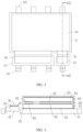
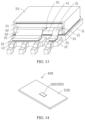
- a chip package module 100 in a first embodiment of this application includes a first conductive frame 11, a second conductive frame 12, and a third conductive frame 13.
- the first conductive frame 11, the second conductive frame 12, and the third conductive frame 13 are disposed at an interval from each other.
- the first conductive frame 11, the second conductive frame 12, and the third conductive frame 13 all have a flat plate form.
- Each of the first conductive frame 11, the second conductive frame 12, and the third conductive frame 13 is connected to a pin 101.
- the pin 101 is configured to electrically connect to another electronic component (for example, an external circuit).
- Materials of the first conductive frame 11, the second conductive frame 12, and the third conductive frame 13 may be conductive metal.
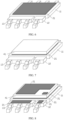
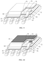
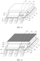
- the chip package module 100 further includes a first bare die 41, a second bare die 42, a first conductive connecting sheet 31, and a second conductive connecting sheet 32.
- the first bare die 41 is disposed on the first conductive frame 11.
- an area of a top surface that is of the first conductive frame 11 and that is used to place the first bare die 41 is larger than an area of the first bare die 41, and the first bare die 41 partially covers a top surface of the first conductive frame 11.
- Solder 21 is disposed between the first bare die 41 and the first conductive frame 11, and an electrical connection is implemented by soldering.
- the first conductive connecting sheet 31 partially covers and is connected to a surface of the first bare die 41 away from the first conductive frame 11, and extends to be lapped on the second conductive frame 12.
- the second conductive connecting sheet 32 partially covers and is connected to the surface of the first bare die 41 away from the first conductive frame 11, and extends to be lapped on the third conductive frame 13.
- the second conductive connecting sheet 32 and the first conductive connecting sheet 31 are disposed at an interval.
- Solder 21 is disposed in regions in which the first conductive connecting sheet 31 is lapped on the first bare die 41 and the second conductive frame 12, and the first conductive connecting sheet 31 is electrically connected to both the first bare die 41 and the second conductive frame 12 by soldering.
- Solder 21 is disposed in regions in which the second conductive connecting sheet 32 is lapped on the first bare die 41 and the third conductive frame 13, and the second conductive connecting sheet 32 is electrically connected to both the first bare die 41 and the third conductive frame 13 by soldering.
- the second bare die 42 is laminated on a surface of the first bare die 41 with the first conductive connecting sheet 31 and the second conductive connecting sheet 32, and is electrically connected to both the first conductive connecting sheet 31 and the second conductive connecting sheet 32.
- the first conductive connecting sheet 31 and the second conductive frame 12 are cooperatively disposed, and the second conductive connecting sheet 32 and the third conductive frame 13 are cooperatively disposed.
- Solder 21 is disposed in regions in which the second bare die 42 is lapped on the first conductive connecting sheet 31 and the second conductive connecting sheet 32, and the second bare die 42 is electrically connected to the first conductive connecting sheet 31 and the second conductive connecting sheet 32 by soldering.
- the first conductive connecting sheet 31 is electrically connected to the first bare die 41 and the second bare die 42.
- the second conductive connecting sheet 32 is also electrically connected to the first bare die 41 and the second bare die 42.
- the chip package module 100 further includes a conductive cover plate 33.
- the conductive cover plate 33 is connected to a surface of the second bare die 42 away from the first conductive frame 11, and extends to be connected to the first conductive frame 11.
- the conductive cover plate 33 includes a flat plate 331 and at least one side plate 333 that is bent and connected to the flat plate 331.
- the flat plate 331 covers the surface of the second bare die 42 away from the first conductive frame 11.
- Each side plate 333 is connected between the flat plate 331 and the first conductive frame 11.
- the conductive cover plate 33 and the first conductive frame 11 are cooperatively disposed.
- Solder 21 is disposed between the flat plate 331 and the second bare die 42, and solder 21 is also disposed between the side plate 333 and the first conductive frame 11.
- the conductive cover plate 33 is electrically connected to the second bare die 42 and the first conductive frame 11 by soldering.
- the conductive cover plate 33 includes three side plates 333 vertically connected to the flat plate 331.
- the side plate 333 is not disposed, to keep the side plate 333 from affecting that the first conductive connecting sheet 31 and the second conductive connecting sheet 32 respectively extend to be lapped on the second conductive frame 12 and the third conductive frame 13.
- the side plates 333 are equivalently supported between the flat plate 331 and the first conductive frame 11, to provide a support force.
- a structure of the side plate 333 includes but is not limited to a right-angle bending (the side plate 333 is vertically connected to the flat plate 331), a step-shaped bending, a support column, and the like.
- the conductive cover plate 33 is connected to the first conductive frame 11 by the three bent side plates 333.
- the three side plates 333 can bear a weight of the conductive cover plate 33 itself and a weight of a plastic package material obtained after a part of the chip package module 100 is packaged in plastic, to relieve stress of the first bare die 41 below to some extent.
- a structure of a chip package module 200 in a second embodiment of this application is basically the same as a structure of the chip package module 100.
- a difference lies in that a conductive cover plate 33 of the chip package module 200 includes only one side plate 333 vertically connected to the flat plate 331. If a side of the first conductive frame 11 on which the second conductive frame 12 and the third conductive frame 13 are disposed is a first side, the unique side plate 333 is disposed on a second side opposite to the first side.
- the single side plate 333 is connected to the first conductive frame 11, which can also play a supporting role and reduce design and manufacturing difficulty of the conductive cover plate 33.
- the first conductive frame 11, the second conductive frame 12, and the third conductive frame 13 are all rectangular plates, and a size of the first conductive frame 11 is larger than a size of the second conductive frame 12 and a size of the third conductive frame 13.
- the second conductive frame 12 and the third conductive frame 13 are located on a same side edge of the first conductive frame 11.
- a pin 101 of the first conductive frame 11 is connected to a side of the first conductive frame 11 away from the second conductive frame 12.
- a pin 101 of the second conductive frame 12 is connected to a side of the second conductive frame 12 away from the first conductive frame 11.
- a pin 101 of the third conductive frame 13 is connected to a side of the third conductive frame 13 away from the first conductive frame 11.
- the first conductive frame 11, the second conductive frame 12, and the third conductive frame 13 have a same thickness. Therefore, when the first bare die 41 is disposed on the first conductive frame 11, a height of the first bare die 41 is larger than that of the second conductive frame 12 and the third conductive frame 13.
- the first conductive connecting sheet 31 is bent and extends from the first bare die 41 to the second conductive frame 12 to be lapped on and cover the second conductive frame 12.
- the second conductive connecting sheet 32 is bent and extends from the first bare die 41 to the third conductive frame 13 to be lapped on and cover the third conductive frame 13.
- the first conductive connecting sheet 31 and the second conductive connecting sheet 32 are spaced from each other. As shown in FIG.
- the first conductive connecting sheet 31 includes two flat parts 310 and a connecting part 311 connected between the two flat parts 310.
- One flat part 310 covers the first bare die 41, and the other flat part 310 covers the second conductive frame 12.
- the connecting part is bent and extends from an end part of each flat part 310.
- the second conductive connecting part also includes two flat parts 310 and a connecting part 311 connected between the two flat parts 310.
- One flat part 310 covers the first bare die 41, and the other flat part 310 covers the third conductive frame 13.
- the connecting part 311 is bent and extends from an end part of each flat part 310.
- the chip package module 100 may further include a plastic package layer (not shown in the figure) for packaging the conductive cover plate 33, the first bare die 41, and the second bare die 42.
- the conductive cover plate 33 may be included inside a plastic package body, or may be partially exposed to air to increase a heat dissipation capability.
- the first conductive connecting sheet 31, the second conductive connecting sheet 32, and the conductive cover plate 33 may be made of a same material.
- the material is a metal material or a solid-state conductive organic material, but is not limited thereto.
- Each of the first bare die 41 and the second bare die 42 includes a plurality of electrodes (not shown in the figure).
- An electrode (a first electrode) of the first bare die 41 is electrically connected to the first conductive frame 11.
- An electrode (a second electrode) of the second bare die 42 is electrically connected to the conductive cover plate 33.
- the first conductive frame 11 is electrically connected to the first bare die 41. Therefore, the first pair of electrodes of the first bare die 41 and the second bare die 42 are electrically connected to the conductive cover plate 33 by the first conductive frame 11.
- signal transmission with an external circuit is implemented through the first conductive frame 11.
- Another electrode (a third electrode) of the first bare die 41 and another electrode (a fourth electrode) of the second bare die 42 are both electrically connected to the first conductive connecting sheet 31.
- the second pair of electrodes of the first bare die 41 and the second bare die 42 are electrically connected by the first conductive connecting sheet 31, and then are electrically connected to the first conductive connecting sheet 31 by the second conductive frame 12 to implement signal transmission with an external circuit.
- Still another electrode (a fifth electrode) of the first bare die 41 and still another electrode (a sixth electrode) of the second bare die 42 are both electrically connected to the second conductive connecting sheet 32.
- the third pair of electrodes of the first bare die 41 and the second bare die 42 are electrically connected by the second conductive connecting sheet 32, and then are electrically connected to the second conductive connecting sheet 32 by the third conductive frame 13, to implement signal transmission with an external circuit.
- first conductive connecting sheet 31 and the second conductive frame 12 are cooperatively disposed and the second conductive connecting sheet 32 and the third conductive frame 13 are cooperatively disposed according to a quantity of pairs of electrodes that need to be electrically connected in the first bare die 41 and the second bare die 42, and may be correspondingly increased or decreased as required.
- first conductive connecting sheet 31 and the second conductive frame 12 and the second conductive connecting sheet 32 and the third conductive frame 13 may both be omitted.
- the second conductive connecting sheet 32 and the third conductive frame 13 may be omitted.
- the first conductive connecting sheet 31, the second conductive connecting sheet 32, and the conductive cover plate 33 are used to implement electrical interconnection between the bare dies 41 and 42 that are vertically laminated, and the two bare dies are packaged inside one device, so that performance of a single device is improved, and a requirement of a high-performance power supply system for a device is met to some extent.
- both the first bare die 41 and the second bare die 42 are MOSFET chips.
- the plurality of electrodes of the first bare die 41 include a source, a drain, and a gate
- the plurality of electrodes of the second bare die 42 also include a source, a drain, and a gate.
- the source, the drain, and the gate of the first bare die 41 are electrically connected in a one-to-one correspondence to the first conductive frame 11, the first conductive connecting sheet 31, and the second conductive connecting sheet 32.
- a specific correspondence connection relationship is not limited.
- the source of the first bare die 41 is electrically connected to any one of the first conductive frame 11, the first conductive connecting sheet 31, and the second conductive connecting sheet 32.
- the drain of the first bare die 41 is electrically connected to one of the remaining two of the first conductive frame 11, the first conductive connecting sheet 31, and the second conductive connecting sheet 32.
- the gate of the first bare die 41 is electrically connected to the last remaining one of the first conductive frame 11, the first conductive connecting sheet 31, and the second conductive connecting sheet 32.
- the source, the drain, and the gate of the second bare die 42 are electrically connected in a one-to-one correspondence to the conductive cover plate 33, the first conductive connecting sheet 31, and the second conductive connecting sheet 32.
- a specific correspondence connection relationship is not limited.
- the source of the second bare die 42 is electrically connected to any one of the conductive cover plate 33, the first conductive connecting sheet 31, and the second conductive connecting sheet 32.
- the drain of the second bare die 42 is electrically connected to one of the remaining two of the conductive cover plate 33, the first conductive connecting sheet 31, and the second conductive connecting sheet 32.
- the gate of the second bare die 42 is electrically connected to the last remaining one of the conductive cover plate 33, the first conductive connecting sheet 31, and the second conductive connecting sheet 32.
- the source of the first bare die 41 is connected in parallel to the source of the second bare die 42.
- the drain of the first bare die 41 is connected in parallel to the drain of the second bare die 42.
- the gate of the first bare die 41 is connected in parallel to the gate of the second bare die 42.
- the three terminals, namely, the sources, the drains, and the gates, of the second bare die 42 and the first bare die 41 that are vertically laminated are connected in parallel.
- the first electrode of the first bare die 41 is the drain and is electrically connected to the first conductive frame 11.
- the third electrode of the first bare die 41 is the gate and is electrically connected to the first conductive connecting sheet 31.
- the fifth electrode of the first bare die 41 is the source and is electrically connected to the second conductive connecting sheet 32.
- the second electrode of the second bare die 42 is the drain and is electrically connected to the conductive cover plate 33.
- the fourth electrode of the second bare die 42 is the gate and is electrically connected to the first conductive connecting sheet 31.
- the sixth electrode of the second bare die 42 is the source and is electrically connected to the second conductive connecting sheet 32.
- the three terminals, namely, the sources, the drains, and the gates, of the second bare die 42 and the first bare die 41 are connected in parallel.
- the first conductive connecting sheet 31, the second conductive connecting sheet 32, and the conductive cover plate 33 are used to implement a parallel connection of the three terminals of the bare dies 41 and 42 that are vertically laminated, so that a single device has vertically laminated chips, and performance of the device is greatly improved.
- sizes and thicknesses of the first bare die 41 and the second bare die 42, and an area of the solder 21 to be coated in the chip package module 100 may be adjusted and designed as required.
- this application further provides a power module 400, including a circuit board 530 and the foregoing chip package modules 100 and 200 located on the circuit board 530.
- the pins 101 of the first conductive frame 11, the second conductive frame 12, and the third conductive frame 13 may all be electrically connected to the circuit board 530.
- this application further provides an electronic device 500, including a housing 510, a circuit board 530 located in the housing 510, and the foregoing chip package modules 100 and 200 located on the circuit board 530.
- this application further provides a method for manufacturing the foregoing chip package module, including the following steps.
- first conductive connecting sheet 31 and the second conductive frame 12 are cooperatively disposed and the second conductive connecting sheet 32 and the third conductive frame 13 are cooperatively disposed according to a quantity of pairs of electrodes that need to be electrically connected in the first bare die 41 and the second bare die 42, and may be correspondingly increased or decreased as required.
- the first conductive frame 11, the second conductive frame 12, and the third conductive frame 13 are all rectangular flat blocks, and a size of the first conductive frame 11 is larger than a size of the second conductive frame 12 and a size of the third conductive frame 13.
- the second conductive frame 12 and the third conductive frame 13 are located on a same side edge of the first conductive frame 11.
- the first conductive frame 11, the second conductive frame 12, and the third conductive frame 13 are all connected to pins 101.
- the pin 101 of the first conductive frame 11 is connected to a side of the first conductive frame 11 away from the second conductive frame 12.
- the pin 101 of the second conductive frame is connected to a side of the second conductive frame 12 away from the first conductive frame 11.
- the pin 101 of the third conductive frame 13 is connected to a side of the third conductive frame 13 away from the first conductive frame 11.
- the first conductive frame 11, the second conductive frame 12, and the third conductive frame 13 may be obtained by cutting a conductive metal plate.
- the pins 101 may also be obtained by processing the conductive metal plate.
- the conductive frames and the pins 101 connected to the conductive frames are integrally formed. However, this application is not limited thereto.
- the first conductive frame 11, the second conductive frame 12, and the third conductive frame 13 have a same thickness.
- that attaching a first bare die 41 to the first conductive frame 11 includes: arranging solder 21 on the first conductive frame 11, placing the first bare die 41 on the solder 21, and then electrically connecting the first bare die 41 to the first conductive frame 11 by soldering, for example, performing heating (a heating temperature generally does not exceed 450 degrees Celsius) to splice the solder 21 between the first bare die 41 and the first conductive frame 11.
- the arranging a first conductive connecting sheet 31 and arranging a second conductive connecting sheet 32 includes: arranging two groups of solder 21 disposed at intervals on the surface of the first bare die 41 away from the first conductive frame 11, arranging solder 21 separately on the second conductive frame 12 and the third conductive frame 13, then placing the first conductive connecting sheet 31 on one group of solder 21 of the first bare die 41 and the solder 21 on the second conductive frame 12, arranging the second conductive connecting sheet 32 on the other group of solder 21 of the first bare die 41 and the solder 21 on the third conductive frame 13, and electrically connecting the first conductive connecting sheet 31 to the first bare die 41 and the second conductive frame 12 by soldering and electrically connecting the second conductive connecting sheet 32 to the first bare die 41 and the third conductive frame 13 by soldering, for example, performing heating (the heating temperature generally does not exceed 450 degrees Celsius) to splice the solder 21 between the first bare die 41 and the first bare die 41 and the first bare die 41 and
- the first conductive connecting sheet 31 needs to match shapes of the first bare die 41 and the first conductive frame 11.
- the first conductive connecting sheet 31 includes two flat parts 310 and a connecting part 311 connected between the two flat parts 310.
- the connecting part 311 is bent and extends from an end part of each flat part 310.
- One flat part 310 covers the first bare die 41, and the other flat part 310 covers the second conductive frame 12.
- a shape of the second conductive connecting part needs to match shapes of the first bare die 41 and the second conductive frame 12.
- the second conductive connecting part also includes two flat parts 310 and a connecting part 311 connected between the two flat parts 310.
- the connecting part 311 is bent and extends from an end part of each flat part 310.
- One flat part 310 covers the first bare die 41, and the other flat part 310 covers the third conductive frame 13.
- the attaching a second bare die 42 includes: separately arranging solder 21 on surfaces of the first conductive connecting sheet 31 and the second conductive connecting sheet 32 away from the first bare die 41, placing the second bare die 42 on the solder 21, and electrically connecting the second bare die 42 to the first conductive connecting sheet 31 and the second conductive connecting sheet 32 by soldering, for example, performing heating to splice the solder 21 between the second bare die 42 and the first conductive connecting sheet 31 and between the second bare die 42 and the second conductive connecting sheet 32.
- the arranging a conductive cover plate 33 includes: arranging solder 21 on the surface of the second bare die 42 away from the first conductive frame 11, placing the flat plate 331 of the conductive cover plate 33 on the solder 21, and electrically connecting the conductive cover plate 33 to the second bare die 42 by soldering, for example, performing heating to splice the solder 21 between the conductive cover plate 33 and the second bare die 42.
Landscapes
- Structures Or Materials For Encapsulating Or Coating Semiconductor Devices Or Solid State Devices (AREA)
Applications Claiming Priority (2)
| Application Number | Priority Date | Filing Date | Title |
|---|---|---|---|
| CN202210194673.XA CN114743957B (zh) | 2022-03-01 | 2022-03-01 | 芯片封装模组及其制备方法、电源模块、电子设备 |
| PCT/CN2022/138513 WO2023165213A1 (zh) | 2022-03-01 | 2022-12-13 | 芯片封装模组及其制备方法、电源模块、电子设备 |
Publications (2)
| Publication Number | Publication Date |
|---|---|
| EP4407680A1 true EP4407680A1 (de) | 2024-07-31 |
| EP4407680A4 EP4407680A4 (de) | 2025-04-30 |
Family
ID=82275670
Family Applications (1)
| Application Number | Title | Priority Date | Filing Date |
|---|---|---|---|
| EP22929640.5A Pending EP4407680A4 (de) | 2022-03-01 | 2022-12-13 | Chipgehäusemodul und herstellungsverfahren dafür, stromversorgungsmodul und elektronische vorrichtung |
Country Status (5)
| Country | Link |
|---|---|
| US (1) | US20240312882A1 (de) |
| EP (1) | EP4407680A4 (de) |
| JP (1) | JP7704478B2 (de) |
| CN (1) | CN114743957B (de) |
| WO (1) | WO2023165213A1 (de) |
Families Citing this family (1)
| Publication number | Priority date | Publication date | Assignee | Title |
|---|---|---|---|---|
| CN114743957B (zh) * | 2022-03-01 | 2026-04-21 | 华为数字能源技术有限公司 | 芯片封装模组及其制备方法、电源模块、电子设备 |
Family Cites Families (8)
| Publication number | Priority date | Publication date | Assignee | Title |
|---|---|---|---|---|
| JP2005302951A (ja) * | 2004-04-09 | 2005-10-27 | Toshiba Corp | 電力用半導体装置パッケージ |
| US20090212405A1 (en) * | 2008-02-26 | 2009-08-27 | Yong Liu | Stacked die molded leadless package |
| US9214417B2 (en) * | 2010-06-18 | 2015-12-15 | Alpha And Omega Semiconductor Incorporated | Combined packaged power semiconductor device |
| CN102593108B (zh) * | 2011-01-18 | 2014-08-20 | 台达电子工业股份有限公司 | 功率半导体封装结构及其制造方法 |
| US20140063744A1 (en) * | 2012-09-05 | 2014-03-06 | Texas Instruments Incorporated | Vertically Stacked Power FETS and Synchronous Buck Converter Having Low On-Resistance |
| US9082868B2 (en) * | 2013-03-13 | 2015-07-14 | Semiconductor Components Industries, Llc | Semiconductor component and method of manufacture |
| CN110504220A (zh) * | 2019-08-26 | 2019-11-26 | 珠海格力电器股份有限公司 | 功率器件封装方法及功率器件封装结构 |
| CN114743957B (zh) * | 2022-03-01 | 2026-04-21 | 华为数字能源技术有限公司 | 芯片封装模组及其制备方法、电源模块、电子设备 |
-
2022
- 2022-03-01 CN CN202210194673.XA patent/CN114743957B/zh active Active
- 2022-12-13 WO PCT/CN2022/138513 patent/WO2023165213A1/zh not_active Ceased
- 2022-12-13 EP EP22929640.5A patent/EP4407680A4/de active Pending
- 2022-12-13 JP JP2024533960A patent/JP7704478B2/ja active Active
-
2024
- 2024-05-22 US US18/671,243 patent/US20240312882A1/en active Pending
Also Published As
| Publication number | Publication date |
|---|---|
| WO2023165213A1 (zh) | 2023-09-07 |
| US20240312882A1 (en) | 2024-09-19 |
| CN114743957B (zh) | 2026-04-21 |
| JP7704478B2 (ja) | 2025-07-08 |
| CN114743957A (zh) | 2022-07-12 |
| JP2024542835A (ja) | 2024-11-15 |
| EP4407680A4 (de) | 2025-04-30 |
Similar Documents
| Publication | Publication Date | Title |
|---|---|---|
| EP2526565B1 (de) | Halbleitergehäusungsmethode | |
| CN101656250B (zh) | 具有立体匹配互连板的紧密封装半导体芯片 | |
| US6847112B2 (en) | Semiconductor device and manufacturing the same | |
| EP4148778B1 (de) | Leistungshalbleitermodul | |
| CN105990266A (zh) | 功率转换电路的封装模块及其制造方法 | |
| US20070108560A1 (en) | Stackable power semiconductor package system | |
| US20240312882A1 (en) | Chip package module, method for manufacturing same, power module, and electronic device | |
| JPWO2020035931A1 (ja) | 半導体モジュール | |
| CN116130477A (zh) | 智能功率模块和具有其的电子设备 | |
| CN116190369A (zh) | 智能功率模块和具有其的电子设备 | |
| CN202487568U (zh) | 半导体模块 | |
| CN101930957A (zh) | 功率半导体器件封装及制造方法 | |
| US20230317685A1 (en) | Packaged electronic device comprising a plurality of power transistors | |
| CN103681669B (zh) | 用于电池组保护mosfet的公共漏极电源夹件 | |
| US11482468B2 (en) | Power module package casing with protrusion supports | |
| US20250105112A1 (en) | Electronic package with integral seal | |
| JP2012074588A (ja) | 半導体パワーモジュールおよびその製造方法 | |
| CN118173546A (zh) | 一种芯片并联堆叠封装结构及其封装方法 | |
| CN104952815B (zh) | 半导体模块以及半导体模块的制造方法 | |
| CN214705919U (zh) | 一种适用于wlcsp芯片的封装结构 | |
| JP2020087998A (ja) | リードフレーム、半導体装置及び半導体装置の製造方法 | |
| US9953890B2 (en) | Semiconductor device | |
| EP4050650A1 (de) | Leistungshalbleitermodulanordnung | |
| US20250046671A1 (en) | Semiconductor apparatus and method for manufacturing semiconductor apparatus | |
| CN119050110B (zh) | 功率器件 |
Legal Events
| Date | Code | Title | Description |
|---|---|---|---|
| STAA | Information on the status of an ep patent application or granted ep patent |
Free format text: STATUS: THE INTERNATIONAL PUBLICATION HAS BEEN MADE |
|
| PUAI | Public reference made under article 153(3) epc to a published international application that has entered the european phase |
Free format text: ORIGINAL CODE: 0009012 |
|
| STAA | Information on the status of an ep patent application or granted ep patent |
Free format text: STATUS: REQUEST FOR EXAMINATION WAS MADE |
|
| 17P | Request for examination filed |
Effective date: 20240426 |
|
| AK | Designated contracting states |
Kind code of ref document: A1 Designated state(s): AL AT BE BG CH CY CZ DE DK EE ES FI FR GB GR HR HU IE IS IT LI LT LU LV MC ME MK MT NL NO PL PT RO RS SE SI SK SM TR |
|
| A4 | Supplementary search report drawn up and despatched |
Effective date: 20250327 |
|
| RIC1 | Information provided on ipc code assigned before grant |
Ipc: H01L 21/60 20060101ALI20250321BHEP Ipc: H01L 23/492 20060101ALI20250321BHEP Ipc: H01L 23/495 20060101ALI20250321BHEP Ipc: H01L 25/07 20060101AFI20250321BHEP |
|
| DAV | Request for validation of the european patent (deleted) | ||
| DAX | Request for extension of the european patent (deleted) |