EP4407419A2 - Berührungsanzeigevorrichtung und anzeigetafel - Google Patents
Berührungsanzeigevorrichtung und anzeigetafel Download PDFInfo
- Publication number
- EP4407419A2 EP4407419A2 EP24168725.0A EP24168725A EP4407419A2 EP 4407419 A2 EP4407419 A2 EP 4407419A2 EP 24168725 A EP24168725 A EP 24168725A EP 4407419 A2 EP4407419 A2 EP 4407419A2
- Authority
- EP
- European Patent Office
- Prior art keywords
- touch
- area
- disposed
- touch electrodes
- display device
- Prior art date
- Legal status (The legal status is an assumption and is not a legal conclusion. Google has not performed a legal analysis and makes no representation as to the accuracy of the status listed.)
- Pending
Links
Images


Classifications
-
- G—PHYSICS
- G06—COMPUTING OR CALCULATING; COUNTING
- G06F—ELECTRIC DIGITAL DATA PROCESSING
- G06F3/00—Input arrangements for transferring data to be processed into a form capable of being handled by the computer; Output arrangements for transferring data from processing unit to output unit, e.g. interface arrangements
- G06F3/01—Input arrangements or combined input and output arrangements for interaction between user and computer
- G06F3/03—Arrangements for converting the position or the displacement of a member into a coded form
- G06F3/041—Digitisers, e.g. for touch screens or touch pads, characterised by the transducing means
- G06F3/0412—Digitisers structurally integrated in a display
-
- G—PHYSICS
- G06—COMPUTING OR CALCULATING; COUNTING
- G06F—ELECTRIC DIGITAL DATA PROCESSING
- G06F3/00—Input arrangements for transferring data to be processed into a form capable of being handled by the computer; Output arrangements for transferring data from processing unit to output unit, e.g. interface arrangements
- G06F3/01—Input arrangements or combined input and output arrangements for interaction between user and computer
- G06F3/03—Arrangements for converting the position or the displacement of a member into a coded form
- G06F3/041—Digitisers, e.g. for touch screens or touch pads, characterised by the transducing means
- G06F3/0416—Control or interface arrangements specially adapted for digitisers
- G06F3/04164—Connections between sensors and controllers, e.g. routing lines between electrodes and connection pads
-
- G—PHYSICS
- G06—COMPUTING OR CALCULATING; COUNTING
- G06F—ELECTRIC DIGITAL DATA PROCESSING
- G06F3/00—Input arrangements for transferring data to be processed into a form capable of being handled by the computer; Output arrangements for transferring data from processing unit to output unit, e.g. interface arrangements
- G06F3/01—Input arrangements or combined input and output arrangements for interaction between user and computer
- G06F3/03—Arrangements for converting the position or the displacement of a member into a coded form
- G06F3/041—Digitisers, e.g. for touch screens or touch pads, characterised by the transducing means
- G06F3/0416—Control or interface arrangements specially adapted for digitisers
- G06F3/0418—Control or interface arrangements specially adapted for digitisers for error correction or compensation, e.g. based on parallax, calibration or alignment
-
- G—PHYSICS
- G06—COMPUTING OR CALCULATING; COUNTING
- G06F—ELECTRIC DIGITAL DATA PROCESSING
- G06F3/00—Input arrangements for transferring data to be processed into a form capable of being handled by the computer; Output arrangements for transferring data from processing unit to output unit, e.g. interface arrangements
- G06F3/01—Input arrangements or combined input and output arrangements for interaction between user and computer
- G06F3/03—Arrangements for converting the position or the displacement of a member into a coded form
- G06F3/041—Digitisers, e.g. for touch screens or touch pads, characterised by the transducing means
- G06F3/044—Digitisers, e.g. for touch screens or touch pads, characterised by the transducing means by capacitive means
- G06F3/0443—Digitisers, e.g. for touch screens or touch pads, characterised by the transducing means by capacitive means using a single layer of sensing electrodes
-
- G—PHYSICS
- G06—COMPUTING OR CALCULATING; COUNTING
- G06F—ELECTRIC DIGITAL DATA PROCESSING
- G06F3/00—Input arrangements for transferring data to be processed into a form capable of being handled by the computer; Output arrangements for transferring data from processing unit to output unit, e.g. interface arrangements
- G06F3/01—Input arrangements or combined input and output arrangements for interaction between user and computer
- G06F3/03—Arrangements for converting the position or the displacement of a member into a coded form
- G06F3/041—Digitisers, e.g. for touch screens or touch pads, characterised by the transducing means
- G06F3/044—Digitisers, e.g. for touch screens or touch pads, characterised by the transducing means by capacitive means
- G06F3/0445—Digitisers, e.g. for touch screens or touch pads, characterised by the transducing means by capacitive means using two or more layers of sensing electrodes, e.g. using two layers of electrodes separated by a dielectric layer
-
- G—PHYSICS
- G06—COMPUTING OR CALCULATING; COUNTING
- G06F—ELECTRIC DIGITAL DATA PROCESSING
- G06F3/00—Input arrangements for transferring data to be processed into a form capable of being handled by the computer; Output arrangements for transferring data from processing unit to output unit, e.g. interface arrangements
- G06F3/01—Input arrangements or combined input and output arrangements for interaction between user and computer
- G06F3/03—Arrangements for converting the position or the displacement of a member into a coded form
- G06F3/041—Digitisers, e.g. for touch screens or touch pads, characterised by the transducing means
- G06F3/044—Digitisers, e.g. for touch screens or touch pads, characterised by the transducing means by capacitive means
- G06F3/0448—Details of the electrode shape, e.g. for enhancing the detection of touches, for generating specific electric field shapes, for enhancing display quality
-
- H—ELECTRICITY
- H10—SEMICONDUCTOR DEVICES; ELECTRIC SOLID-STATE DEVICES NOT OTHERWISE PROVIDED FOR
- H10K—ORGANIC ELECTRIC SOLID-STATE DEVICES
- H10K50/00—Organic light-emitting devices
- H10K50/80—Constructional details
- H10K50/86—Arrangements for improving contrast, e.g. preventing reflection of ambient light
- H10K50/865—Arrangements for improving contrast, e.g. preventing reflection of ambient light comprising light absorbing layers, e.g. light-blocking layers
-
- H—ELECTRICITY
- H10—SEMICONDUCTOR DEVICES; ELECTRIC SOLID-STATE DEVICES NOT OTHERWISE PROVIDED FOR
- H10K—ORGANIC ELECTRIC SOLID-STATE DEVICES
- H10K59/00—Integrated devices, or assemblies of multiple devices, comprising at least one organic light-emitting element covered by group H10K50/00
- H10K59/30—Devices specially adapted for multicolour light emission
- H10K59/38—Devices specially adapted for multicolour light emission comprising colour filters or colour changing media [CCM]
-
- H—ELECTRICITY
- H10—SEMICONDUCTOR DEVICES; ELECTRIC SOLID-STATE DEVICES NOT OTHERWISE PROVIDED FOR
- H10K—ORGANIC ELECTRIC SOLID-STATE DEVICES
- H10K59/00—Integrated devices, or assemblies of multiple devices, comprising at least one organic light-emitting element covered by group H10K50/00
- H10K59/40—OLEDs integrated with touch screens
-
- G—PHYSICS
- G06—COMPUTING OR CALCULATING; COUNTING
- G06F—ELECTRIC DIGITAL DATA PROCESSING
- G06F2203/00—Indexing scheme relating to G06F3/00 - G06F3/048
- G06F2203/041—Indexing scheme relating to G06F3/041 - G06F3/045
- G06F2203/04111—Cross over in capacitive digitiser, i.e. details of structures for connecting electrodes of the sensing pattern where the connections cross each other, e.g. bridge structures comprising an insulating layer, or vias through substrate
Definitions
- Embodiments relate to a touch display device and a display panel.
- Display devices used in computer monitors, TVs, and the like may include self-emitting display devices, such as organic light-emitting displays, vacuum fluorescent displays (VFDs), field emission displays (FEDs), and plasma display panels, and non-self-emitting display devices, such as liquid crystal display (LCD) devices, which need a light source.
- self-emitting display devices such as organic light-emitting displays, vacuum fluorescent displays (VFDs), field emission displays (FEDs), and plasma display panels
- non-self-emitting display devices such as liquid crystal display (LCD) devices, which need a light source.
- LCD liquid crystal display
- a liquid crystal display device includes two substrates respectively having an electrode generating an electric field and a liquid crystal layer disposed between the two substrates and having dielectric anisotropy.
- the LCD device generates an electric field in the liquid crystal layer by applying a voltage to the electrodes generating an electric field and adjusts the strength of the electric field by changing the voltage, so that the transmissivity of light passing through the liquid crystal layer is adjusted, thereby displaying an intended image.
- Such a liquid crystal display device includes a data driving circuit receiving image data from an external source, generating a data voltage, and supplying the data voltage to corresponding pixels of a liquid crystal display panel through data lines, a gate driving circuit generating and supplying a gate signal so that the pixels of the liquid crystal display panel are driven in respective lines, and a backlight unit disposed at the rear of the liquid crystal display panel to light the liquid crystal display panel.
- LEDs light-emitting diodes
- in-cell touch display devices respectively having components of a touchscreen disposed inside (or embedded in) a display panel thereof have been developed and used in order to provide a thin profile to mobile terminals, such as a smartphone and tablet personal computer (PC).
- mobile terminals such as a smartphone and tablet personal computer (PC).
- common electrodes designed for the driving of pixels are also used as touch sensing electrodes.
- a common voltage is provided to thin-film transistors (TFTs) during display driving periods, while a touch driving signal is supplied to the common electrodes serving as the touch electrodes during touch sensing periods.
- TFTs thin-film transistors
- small touch display devices such as watches, vehicle instrument panels, and smartphones
- the inventors of the present disclosure have recognized that undesirable short circuits may frequently occur between metal layers provided inside the small touch display devices as the industry continues to try to miniaturize the size of the touch display devices.
- the thickness of the color filters may be increased.
- the inventors have realized that the increase of thickness of the color filters may reduce the thickness of a planarization layer located between touch lines provided over the color filters, and common electrodes which thereby causes short circuit defects.
- a touch display device and a display panel capable of preventing short circuit defects between touch electrodes and touch lines are provided.
- a touch display device and a display panel having a structure in which a bridge pattern connecting touch electrodes may be provided in an open area in which a single color filter is provided, so as not to overlap an area in which a plurality of color filters are provided, thereby preventing short circuit defects between the touch electrodes and touch lines and enabling accurate touch sensing.
- a touch display device may include: a display panel including an open area of a subpixel in which a single color filter is disposed to display an image and a black strip area in which a plurality of color filters overlap each other to block light emission; a plurality of touch electrodes disposed inside the display panel and separated from each other; a plurality of touch lines connected to the plurality of touch electrodes to apply a touch driving signal to the plurality of touch electrodes; and at least one bridge pattern disposed in the open area and connected to touch electrodes disposed in adjacent subpixels, among the plurality of touch electrodes.
- the bridge pattern may be provided on the same layer and made of the same or substantially the same material as the touch electrodes
- the bridge pattern may be disposed in a middle portion of an outer circumference of the open area with respect to a direction of one side of the open area.
- the bridge pattern may be disposed in a middle portion of the open area with respect to a longitudinal direction of a touch line in the subpixel, among the plurality of touch lines.
- the touch display device may further include an open pattern provided in the black strip area to separate the touch electrodes disposed in the adjacent subpixels.
- a display panel may include: a plurality of subpixels; a plurality of touch electrodes performing touch sensing on the plurality of subpixels; open areas in each of which a single color filter is provided in a corresponding subpixel among the plurality of subpixels to emit light (e.g., to display an image); a black strip area in which a plurality of color filters overlap each other in the plurality of subpixels to block light emission; and at least one bridge pattern disposed in an open area and connected to touch electrodes disposed in adjacent subpixels, among the plurality of touch electrodes.
- the at least one bridge pattern may be provided on the same layer and made of the same or substantially the same material as the touch electrodes.
- the at least one bridge pattern may be disposed in a middle portion of an outer circumference of the open area in a direction of one side of the open area.
- the at least one bridge pattern may be disposed in a middle portion of the open area with respect to a middle portion of an outer circumference of the open area in a longitudinal direction of a touch line in the subpixel, among the plurality of touch lines.
- An open pattern separating the touch electrodes disposed in the adjacent subpixels may be provided in the black strip area.
- a touch display device may include: a display panel including: an open area of a subpixel configured to emit light; a single color filter disposed in the open area; a black strip area adjacent to the open area; and a plurality of color filters overlapped with each other in the black strip area, the black strip area blocking light emission at least partially due to the overlapping of the plurality of color filters; a plurality of touch electrodes disposed inside the display panel and separated from each other; a plurality of touch lines connected to the plurality of touch electrodes, respectively, to apply a touch driving signal to the plurality of touch electrodes; and at least one bridge pattern disposed in the open area and connected to touch electrodes disposed in adjacent subpixels, among the plurality of touch electrodes.
- the at least one bridge pattern may be provided on the same layer and made of the same or substantially the same material as the touch electrodes.
- the at least one bridge pattern may be disposed in a middle portion of an outer circumference of the open area with respect to a direction of one side of the open area.
- the at least one bridge pattern may be disposed in a middle portion of the open area with respect to a longitudinal direction of a touch line in the subpixel, among the plurality of touch lines.
- the touch display device may further include an open pattern provided in the black strip area to separate the touch electrodes disposed in the adjacent subpixels.
- the touch display device and the display panel may prevent short circuit defects between touch electrodes and touch lines.
- the touch display device and the display panel may have a structure in which a bridge pattern connecting touch electrodes may be provided in an open area in which a single color filter is provided, so as not to overlap an area in which a plurality of color filters are provided, thereby preventing short circuit defects between the touch electrodes and touch lines and enabling accurate touch sensing.
- first element is connected or coupled to
- contacts or overlaps etc.
- second element it should be interpreted that, not only can the first element “be directly connected or coupled to” or “directly contact or overlap” the second element, but a third element can also be “interposed” between the first and second elements, or the first and second elements can “be connected or coupled to,” “contact or overlap,” etc., each other via a fourth element.
- the second element may be included in at least one of two or more elements that "are connected or coupled to,” “contact or overlap,” etc., each other.
- time relative terms such as “after,” “subsequent to,” “next,” “before,” and the like, are used to describe processes or operations of elements or configurations, or flows or steps in operating, processing, manufacturing methods, these terms may be used to describe nonconsecutive or non-sequential processes or operations unless the term “directly” or “immediately” is used together with the term.
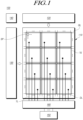
- FIG. 1 is a schematic diagram illustrating the configuration of a touch display device according to embodiments.
- a touch display device 100 is a device able to provide an image display function and a touch sensing function.
- the touch display device 100 may be a medium or large display device, such as a TV or a monitor, having a touch sensing function for a touch input, or may be a mobile device, such as a smartphone or a tablet personal computer (PC).
- a medium or large display device such as a TV or a monitor, having a touch sensing function for a touch input
- a mobile device such as a smartphone or a tablet personal computer (PC).
- the touch display device 100 includes a display panel 110, a data driving circuit 120, a gate driving circuit 130, a timing controller 140, and the like to provide the image display function.
- the display panel 110 may include a plurality of data lines DL extending in a first direction (e.g., a column direction) and a plurality of gate lines GL extending in a second direction (e.g., a row direction).
- a first direction e.g., a column direction
- a plurality of gate lines GL extending in a second direction (e.g., a row direction).
- the data driving circuit 120 drives the plurality of data lines DL, while the gate driving circuit 130 drives the plurality of gate lines GL.
- the timing controller 140 controls the data driving circuit 120 and the gate driving circuit 130. In this regard, the timing controller 140 supplies a variety of signals to the data driving circuit 120 and the gate driving circuit 130.
- the timing controller 140 starts scanning process at points in time realized by respective frames, outputs image data obtained by converting input image data supplied by an external source into a data signal format readable by the data driving circuit 120, and controls data driving at appropriate points in time in response to the scanning.
- the timing controller 140 may be a controller used in typical display technology or may be a control device including such a controller and performing other control functions.
- the data driving circuit 120 drives the plurality of data lines DL by supplying a data voltage to the plurality of data lines DL.
- the data driving circuit 120 may also be referred to as a "source driving circuit (SDIC)."
- the gate driving circuit 130 sequentially drives the plurality of gate lines GL by sequentially supplying a scan signal to the plurality of gate lines GL.
- the gate driving circuit 130 may also be referred to as a "scan driving circuit.”
- the gate driving circuit 130 sequentially supplies the scan signal having an on or off voltage to the plurality of gate lines GL, under the control of the timing controller 140.
- the data driving circuit 120 converts the image data, received from the timing controller 140, into an analog data voltage, and supplies the analog data voltage to the plurality of data lines DL.
- the data driving circuit 120 may be located on one side of (e.g., above or below) the display panel 110 or may be located on both sides of (e.g., above and below) the display panel 110 depending on the driving method, the design of the panel, or the like.
- the gate driving circuit 130 may be located on one side (e.g., to the left or right) of the display panel 110 or may be located on both sides (e.g., to the left and right) of the display panel 110 depending on the driving method, the design of the panel, or the like.
- the data driving circuit 120 may include at least one data driving integrated circuit to drive the plurality of data lines.
- Each of the data driving integrated circuits may be connected to a bonding pad of the display panel 110 by a tape-automated bonding (TAB) method or a chip-on-glass (COG) method, may be directly mounted on the display panel 110, or in some cases, may be provided as an integrated portion of the display panel 110.
- TAB tape-automated bonding
- COG chip-on-glass
- each of the data driving integrated circuits may be implemented using a chip-on-film (COF) structure mounted on a film connected to the display panel 110.
- COF chip-on-film
- Each of the data driving integrated circuits may include a shift register, a latch circuit, a digital-to-analog converter (DAC), an output buffer, and the like.
- DAC digital-to-analog converter
- the gate driving circuit 130 may include at least one gate driving integrated circuit.
- Each of the gate driving integrated circuits may be connected to a bonding pad of the display panel 110 by a TAB method or a COG method, may be implemented using a gate-in-panel (GIP) structure directly mounted on the display panel 110, or in some cases, may be provided as an integrated portion of the display panel 110.
- GIP gate-in-panel
- each of the gate driving integrated circuits may be implemented using a COF structure mounted on a film connected to the display panel 110.
- the touch display device 100 may be various types of devices, such as a liquid crystal display (LCD) device, an organic light-emitting display device, a plasma display panel, or the like.
- LCD liquid crystal display
- OLED organic light-emitting display
- plasma display panel or the like.
- Each of subpixels SP arranged in the display panel 110 may include circuit components, such as a transistor.
- the touch display device 100 may include a touch system for providing a touch sensing function.
- the touch system may include a plurality of touch electrodes arranged in the form of a matrix to serve as touch electrodes, a touch circuit 150 sensing touches by driving the plurality of touch electrodes, and the like.
- the touch circuit 150 may be comprised of a plurality of modules (e.g., a touch driving circuit and a touch sensing circuit). Some or all of the plurality of modules may be included in the data driving integrated circuits of the data driving circuit 120 or may form separate integrated circuits together with the data driving circuit 120.
- the touch circuit 150 may sequentially drive the plurality of touch electrodes TE by sequentially supplying a touch driving signal to the plurality of touch electrodes TE and receive touch sensing signals from the touch electrodes TE to which the touch driving signal has been applied.
- the touch circuit 150 may detect a touch event (e.g., whether or not a touch has been made) and touch coordinates, on the basis of the touch sensing signals received from the plurality of touch electrodes TE.
- a touch event e.g., whether or not a touch has been made
- touch coordinates on the basis of the touch sensing signals received from the plurality of touch electrodes TE.
- the touch driving signal may have, for example, a pulse-width modulation waveform having two or more voltage levels.
- the touch sensing signals received from the plurality of touch electrodes TE may differ depending on whether or not a touch has been made on a corresponding touch electrode TE or surroundings thereof by a pointer, such as a finger or a pen.
- the touch circuit 150 may detect the touch event and the touch coordinates by determining a change in capacitance (or voltage or electric charge) of the touch electrodes TE, on the basis of the touch sensing signals.
- a plurality of touch lines TL are connected to the plurality of touch electrodes TE to supply the touch driving signal to the plurality of touch electrodes TE.
- the touch system may further include a switch circuit 160, by which the touch lines TL connected to the plurality of touch electrodes TE are sequentially connected to the touch circuit 150, in order to sequentially supply the touch driving signal to the plurality of touch electrodes TE.
- Such a switch circuit 160 may be implemented as at least one multiplexer.
- Each of the plurality of touch electrodes TE may be provided in the form of a block.
- each of the touch electrodes TE may be the same as or correspond to the size of each of the subpixels SP. Alternatively, the size of each of the touch electrodes TE may be greater than the size of each of the subpixels SP. That is, the area of each of the touch electrodes TE may have a size corresponding to the area of two or more subpixels SP.
- the number of the touch electrodes TE to be driven for the touch sensing may be reduced.
- the touch driving and the touch sensing related to the touch driving may be efficiently and rapidly performed.
- the plurality of touch electrodes TE may be disposed inside (or embedded in) the display panel 110.
- the display panel 110 may be referred to as including a touchscreen or a touchscreen panel embedded therein. That is, the display panel 110 may be a display panel 110 with an in-cell or on-cell touchscreen embedded therein.
- the touch display device 100 may operate in display mode to provide the image display function or operate in touch mode to provide the touch sensing function.
- the plurality of touch electrodes TE may be used as display electrodes in image display periods, i.e., time periods corresponding to the image display mode, while operating as touch sensors in touch sensing periods, i.e., time periods corresponding to the touch mode.
- the plurality of touch electrodes TE may operate as common electrodes, i.e., an example of the display electrodes to which a common voltage is applied.
- the common voltage corresponds to a pixel voltage applied to pixel electrodes.
- the plurality of touch lines TL may pass through the touch electrodes TE.
- the touch lines TL may be connected to the touch electrodes TE to provide the touch sensing signals to the touch circuit 150.
- the touch lines TL may apply the common voltage to the touch electrodes TE in the display mode and provide the touch sensing signals to the touch circuit 150.
- At least one data line (DL) may be disposed between the touch lines TL.
- the touch lines TL may be provided to reach an area connected to the touch electrodes TE or pass through the entire area in which the touch electrodes TE are disposed, depending on the configuration thereof. In other embodiments, the touch lines TL may be provided to reach an area connected to the touch electrodes TE or pass through at least a portion of the area in which the touch electrodes TE are disposed.
- a single touch line TL may be disposed in each of the touch electrodes TE.
- a contact hole connecting the touch line TL and the touch electrode TE may be provided.
- the contact hole may be provided as a plurality of contact holes to improve the efficiency of the connection or may be a single contact hole.
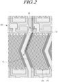
- FIG. 2 is a diagram illustrating a planar structure of the display panel of the touch display device
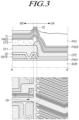
- FIG. 3 is a diagram illustrating the cross-section of an area between adjacent subpixels in which touch electrodes are connected, taken along line A-A' in the display panel illustrated in FIG. 2 , as well as a planar structure of the same area.
- the touch display device 100 may include open areas OA of the subpixels SP in each of which a color filter is provided as a single layer to emit a corresponding color of light and a black strip area BS in which color filters are stacked on each other to prevent light from leaking from circuit portions at the boundaries of the subpixels SP.
- Circuit elements such as a driving transistor, are disposed in the black strip area BS.
- a first insulating layer PAS 1 and a gate electrode layer GATE are sequentially disposed on a substrate SUB, and a gate insulating layer GI is provided to cover the gate electrode layer GATE.
- the substrate SUB may be a glass substrate or a plastic substrate, while the gate electrode layer GATE may have a single-layer structure or a multilayer structure made of one selected from among, but not limited to, Mo, Al, Cr, Au, Ti, Ni, Nd, Cu, and alloys thereof.
- the gate insulating layer GI may be made of an inorganic insulating material, such as silicon dioxide (SiO 2 ), silicon nitride (SiNx), or silicon oxynitride (SiON), or may have a multilayer structure of SiO 2 , SiNx, and SiON.
- silicon dioxide SiO 2
- SiNx silicon nitride
- SiON silicon oxynitride
- Color filters CF (in the example shown, CF 1, CF2, and CF3) for displaying colors are provided over the gate insulating layer GI.
- the color filters CF may have an array of three colors, e.g., red (R), green (G), and blue (B), or an array of four colors, e.g., red (R), green (G), blue (B), and white (W).
- R red
- G green
- B blue
- W white
- an array of color filters CF1, CF2, and CF3 of three colors R, G, and B is illustrated.
- a second insulating layer PAS2 is disposed over the color filters CF, and the touch lines TL are disposed over the second insulating layer PAS2.
- a third insulating layer PAS3 and a planarization layer PAC may be provided over the touch lines TL to insulate the touch lines TL from the pixel electrodes PE or the touch electrodes TE.
- the planarization layer PAC may be an organic film made of, for example, a photo acrylic material, or may be an inorganic film made of, for example, silicon nitride (SiNx).
- the pixel electrodes PE and the touch electrodes TE are provided over the planarization layer PAC.
- the pixel electrodes PE may be connected to source/drain electrodes via contact holes.
- the pixel electrodes PE and the touch electrodes TE may be disposed on different layers or on the same layer.
- the touch electrodes TE correspond to the common electrodes to which the common voltage is applied during display driving periods.
- the touch electrodes TE may have a linear shape or a zigzag shape having one or more bends.
- the pixel electrodes PE may have a linear shape or a zigzag shape having one or more bends.
- the pixel electrodes PE may have a finger pattern, in which case the touch electrodes TE may also have a finger pattern according to the shape of the pixel electrodes PE.
- the touch electrodes TE and the pixel electrodes PE may be made of, for example, a transparent conductive material, such as indium tin oxide (ITO).
- the touch electrodes TE and the touch lines TL are insulated by the planarization layer PAC disposed in an area in which the touch electrodes TE overlap the touch lines TL.
- the color filters CF displaying specific colors have a grid-shaped structure with a predetermined thickness (or a selected thickness in other embodiments) so as to at least partially surround the respective subpixels SP.
- each of the open areas OA displaying the color red (R), green (G), blue (B), or white (W) is an area in which a color filter CF corresponding to each color is provided as a single layer
- the black strip area BS is an area in which two or more of the red, green, and blue color filters CF or the red, green, blue, and white color filters CF overlap.
- the touch electrodes TE in the adjacent subpixels SP are connected to each other by a bridge pattern TB to form a single structure.
- the bridge pattern TB is provided in the black strip area BS.
- the black strip area BS is comprised of double layers of overlapping color filters CF.
- the thickness of the color filters CF in the black strip area BS is greater than the thickness of the single layer of the color filter in each of the open areas OA.
- the color filters CF protrude upward in the area in which the bridge pattern TB is provided, due to the overlapping of the three color filters CF, e.g., the red color filter CF 1, the green color filter CF2, and the blue color filter CF3, in the area in which the bridge pattern TB is provided is illustrated.
- the thickness of the planarization layer PAC provided in the black strip area BS is smaller than the thickness of the planarization layer PAC provided in the open areas OA.
- the distance between the touch electrodes TE provided over the planarization layer PAC and the touch lines TL provided below the planarization layer PAC is reduced.
- the touch electrodes TE and the touch lines TL may be short-circuited in an unintended area.
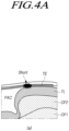
- FIGs. 4A and 4B illustrate an example of two views in which a touch electrode and a touch line are short-circuited in the black strip area of the touch display device.
- the black strip area BS has a structure in which a plurality of color filters CF overlap, and thus, the thickness of the color filters CF in the black strip area BS is greater than the thickness of a single color filter CF in an active area.
- the thickness of the planarization layer PAC provided over the touch lines TL in the black strip area BS is smaller than the thickness of the planarization layer PAC provided in each of the open areas OA.
- the bridge pattern TB may cause a short circuit between the touch electrode TE and the touch line TL in the area between the adjacent subpixels in which the touch electrodes TE are connected (shown in FIG. 4A ).
- the plurality of touch lines TL pass over the touch electrodes TE to which the common voltage is applied during the display driving periods, whereas a single touch line TL is connected to each of the touch electrodes TE.
- the contact hole connecting a single touch electrode TE and a single touch line TL may be provided as a plurality of contact holes for the efficiency of the connection.
- a single touch line TL is connected to two or more touch electrodes TE due to a short circuit in the black strip area BS, an area that has actually been touched may not be able to be determined, and thus, a touch error may occur (shown in FIG. 4B ).
- the bridge pattern TB connecting the touch electrodes TE in the adjacent subpixels SP is provided in the open areas OA in each of which the single color filter CF is disposed, but is not provided in the black strip area BS in which the plurality of color filters CF overlap.
- the planarization layer PAC between the touch electrodes TE and the touch lines TL may have a thickness sufficient to prevent touch sensing errors caused by short circuits between the touch electrodes TE and the touch lines TL.
- FIG. 5 is a diagram illustrating a planar structure of the display panel of the touch display device according to embodiments.
- FIG. 6 is a diagram illustrating the cross-section of an area between adjacent subpixels of the display panel of the touch display device according to embodiments, taken along line B-B' in FIG. 5 and corresponding to an open pattern separating the touch electrodes in the adjacent subpixels and a bridge pattern connecting the touch electrodes in the adjacent subpixels, as well as a planar structure of the same area.
- the display panel 110 may include a plurality of subpixels SP arranged in the form of a matrix.
- the display panel 110 may include the open areas OA in each of which a color filter CF is provided as a single layer in a subpixel SP to generate light having a corresponding color and the black strip area BS preventing light from leaking from circuit portions at the boundaries of the subpixels SP.
- two or more color filters CF are stacked on each other to prevent light leakage.
- the first insulating layer PAS1 and the gate electrode layer GATE are sequentially disposed on the substrate SUB, and the gate insulating layer GI is provided to cover the gate electrode layer GATE.
- the color filters CF displaying colors are provided over the gate insulating layer GI.
- the second insulating layer PAS2 is disposed over the color filters CF, and the touch lines TL are disposed over the second insulating layer PAS2.
- the third insulating layer PASS and the planarization layer PAC may be provided over the touch lines TL to insulate the touch lines TL from the pixel electrodes PE or the touch electrodes TE.
- the pixel electrodes PE and the touch electrodes TE are provided over the planarization layer PAC.
- the pixel electrodes PE may be connected to source/drain electrodes via contact holes.
- the color filters CF displaying specific colors have a grid-shaped structure with a predetermined thickness (or a selected thickness in other embodiments) to at least partially surround the respective subpixels SP.
- each of the open areas OA respectively displaying a color red (R), green (G), blue (B), or white (W) is provided with a single color filter layer corresponding to each color (wherein the single green color filter CF2 is provided as an example).
- the black strip area BS is an area in which two or more of the red, green, and blue color filters CF or the red (R), green (G), blue (B), and white (W) color filters CF overlap.
- the thickness of the color filters CF in the black strip area BS is greater than the thickness of the single color filter CF provided in each of the open areas OA.
- the thickness of the planarization layer PAC provided in the black strip area BS is smaller than the thickness of the planarization layer PAC provided in each of the open areas OA.
- the bridge pattern TB connecting the touch electrodes TE disposed in the adjacent subpixels SP is provided in the open areas OA in each of which the single color filter CF is disposed, but is not provided in the black strip area BS in which the color filters CF overlap and are stacked on each other.
- the planarization layer PAC may have a thickness sufficient to prevent a short circuit that would otherwise occur between the touch electrodes TE and the touch lines TL below the planarization layer PAC.
- the bridge pattern TB provided in the open areas OA of the subpixels SP may be formed such that a single bridge of the bridge pattern TB is provided for a single subpixel SP.
- the bridge pattern TB i.e., a component connecting adjacent touch electrodes TE, may be provided on the same layer and made of the same or substantially the same material as the touch electrodes TE.
- the bridge pattern TB may be provided in middle portions of the outer circumferential lines of the open areas OA, to which the touch electrodes TE are adjacent, for the purpose of efficient design and the symmetry of the display panel 110, and reduced or minimized interference with the other components.
- the vertical direction may refer to a longitudinal direction of the touch line TL in the unit subpixel SP.
- the bridge pattern TB connecting the touch electrodes TE in the adjacent subpixels SP is not provided in the black strip area BS, whereas an open pattern TO separating the adjacent subpixels SP located on both sides of the data lines DL is provided in the black strip area BS.
- the first insulating layer PAS1 and the gate electrode layer GATE are provided on the substrate SUB, and the gate insulating layer GI are provided to cover the gate electrode layer GATE.
- the color filters CF1, CF2, and CF3 for displaying colors are provided over the gate insulating layer GI.
- the thickness of the black strip area BS is increased, such that the thickness of the planarization layer PAC provided in the upper portion of the black strip area BS is reduced.
- the open pattern TO is provided in a portion of the black strip area BS, through which the touch lines TL pass, so as to separate the touch electrodes TE in the adjacent subpixels SP from each other.
- the bridge pattern TB connecting the touch electrodes TE in the adjacent subpixels SP is not provided in the black strip area BS, such that the touch electrodes TE in the adjacent subpixels SP remain separated from each other.
- the touch lines TL are provided but none of the touch electrodes TE is provided over an area in which the first color filter CF1, the second color filter CF2, and the third color filter CF3 overlap each other or an area in which two or more color filters CF overlap each other.
- the thickness of the third insulating layer PASS or the planarization layer PAC provided over the area in which the first color filter CF1 overlaps the second color filter CF2 is reduced, the problem of the touch lines TL being short-circuited to the touch electrodes TE may be prevented.
- the touch electrodes TE provided in the adjacent subpixels SP may be connected to each other via the bridge pattern TB to form a single structure.
- the bridge pattern TB is provided in the open areas OA of the subpixels SP.
- a data line is disposed between subpixels SP adjacent to each other in the horizontal direction.
- the subpixels SP located on both sides of the data lines correspond to the open areas OA respectively emitting a specific color of light.
- a single color filter CF is provided as a single layer to display a specific color of light.
- the plurality of color filters CF1, CF2, and CF3 do not overlap each other.
- the third insulating layer PASS or the planarization layer PAC provided over each of the color filters CF may have a sufficient margin of thickness.
- the touch electrodes TE are provided over the planarization layer PAC having the sufficient margin of thickness and in an area overlapping the touch lines TL, the touch electrodes TE have a sufficient distance D to the touch lines TL provided under the planarization layer PAC. Thus, short circuit defects between the touch electrodes TE and the touch lines TL may be prevented.
- the bridge pattern TB connecting the touch electrodes TE in the adjacent subpixels SP may be provided such that a single bridge of the bridge pattern TB is provided for a single subpixel SP.
- the bridge pattern TB may be provided in middle portions of the outer circumferential lines of the open areas OA, for the purpose of efficient design and the symmetry of the display panel 110, and reduced or minimized interference with the other components.
- embodiments of the present disclosure are applicable to self-emitting display devices, such as organic light-emitting displays, and non-self-emitting display devices, such as liquid crystal display (LCD) devices.
- self-emitting display devices such as organic light-emitting displays
- non-self-emitting display devices such as liquid crystal display (LCD) devices.
- LCD liquid crystal display
- Example 1 A touch display device, comprising: a display panel including: an open area of a subpixel configured to emit light; a single color filter disposed in the open area; a black strip area adjacent to the open area; and a plurality of color filters overlapped with each other in the black strip area, the black strip area blocking light emission at least partially due to the overlapping of the plurality of color filters; a plurality of touch electrodes disposed inside the display panel and separated from each other; a plurality of touch lines connected to the plurality of touch electrodes, respectively, to apply a touch driving signal to the plurality of touch electrodes; and at least one bridge pattern disposed in the open area and connected to touch electrodes disposed in adjacent subpixels, among the plurality of touch electrodes.
- Example 2 The touch display device according to Example 1, wherein the at least one bridge pattern is provided on the same layer and made of the same or substantially the same material as the touch electrodes.
- Example 3 The touch display device according to Example 1 or 2, wherein the at least one bridge pattern is disposed in a middle portion of an outer circumference of the open area with respect to a direction of one side of the open area.
- Example 4 The touch display device according to any one of Examples 1 to 3, wherein the at least one bridge pattern is disposed in a middle portion of the open area with respect to a longitudinal direction of a touch line in the subpixel, among the plurality of touch lines.
- Example 5 The touch display device according to any one of Examples 1 to 4, further comprising an open pattern provided in the black strip area to separate the touch electrodes disposed in the adjacent subpixels.
- Example 6 A display panel, comprising: a plurality of subpixels; a plurality of touch electrodes configured to perform touch sensing on the plurality of subpixels; open areas in each of which a single color filter is provided in a corresponding subpixel among the plurality of subpixels to emit light; a black strip area in which a plurality of color filters overlap each other in the plurality of subpixels to block light emission; and at least one bridge pattern disposed in an open area and connected to touch electrodes disposed in adjacent subpixels, among the plurality of touch electrodes.
- Example 7 The display panel according to Example 6, wherein the at least one bridge pattern is provided on the same layer and made of the same or substantially the same material as the touch electrodes.
- Example 8 The display panel according to Example 6 or 7, wherein the at least one bridge pattern is disposed in a middle portion of an outer circumference of the open area in a direction of one side of the open area.
- Example 9 The display panel according to any one of Examples 6 to 8, wherein the at least one bridge pattern is disposed in a middle portion of the open area with respect to a middle portion of an outer circumference of the open area in a longitudinal direction of a touch line in the subpixel, among the plurality of touch lines.
- Example 10 The display panel according to any one of Examples 6 to 9, wherein an open pattern separating the touch electrodes disposed in the adjacent subpixels is provided in the black strip area.
Landscapes
- Engineering & Computer Science (AREA)
- General Engineering & Computer Science (AREA)
- Theoretical Computer Science (AREA)
- Physics & Mathematics (AREA)
- Human Computer Interaction (AREA)
- General Physics & Mathematics (AREA)
- Computer Networks & Wireless Communication (AREA)
- Quality & Reliability (AREA)
- Optics & Photonics (AREA)
- Devices For Indicating Variable Information By Combining Individual Elements (AREA)
- Liquid Crystal (AREA)
- Position Input By Displaying (AREA)
Applications Claiming Priority (2)
| Application Number | Priority Date | Filing Date | Title |
|---|---|---|---|
| KR1020190176608A KR102891728B1 (ko) | 2019-12-27 | 2019-12-27 | 터치 디스플레이 장치, 및 디스플레이 패널 |
| EP20216458.8A EP3842903B1 (de) | 2019-12-27 | 2020-12-22 | Berührungsanzeigevorrichtung und anzeigetafel |
Related Parent Applications (2)
| Application Number | Title | Priority Date | Filing Date |
|---|---|---|---|
| EP20216458.8A Division-Into EP3842903B1 (de) | 2019-12-27 | 2020-12-22 | Berührungsanzeigevorrichtung und anzeigetafel |
| EP20216458.8A Division EP3842903B1 (de) | 2019-12-27 | 2020-12-22 | Berührungsanzeigevorrichtung und anzeigetafel |
Publications (2)
| Publication Number | Publication Date |
|---|---|
| EP4407419A2 true EP4407419A2 (de) | 2024-07-31 |
| EP4407419A3 EP4407419A3 (de) | 2024-10-30 |
Family
ID=73856794
Family Applications (2)
| Application Number | Title | Priority Date | Filing Date |
|---|---|---|---|
| EP24168725.0A Pending EP4407419A3 (de) | 2019-12-27 | 2020-12-22 | Berührungsanzeigevorrichtung und anzeigetafel |
| EP20216458.8A Active EP3842903B1 (de) | 2019-12-27 | 2020-12-22 | Berührungsanzeigevorrichtung und anzeigetafel |
Family Applications After (1)
| Application Number | Title | Priority Date | Filing Date |
|---|---|---|---|
| EP20216458.8A Active EP3842903B1 (de) | 2019-12-27 | 2020-12-22 | Berührungsanzeigevorrichtung und anzeigetafel |
Country Status (4)
| Country | Link |
|---|---|
| US (2) | US11402936B2 (de) |
| EP (2) | EP4407419A3 (de) |
| KR (1) | KR102891728B1 (de) |
| CN (1) | CN113050821B (de) |
Families Citing this family (5)
| Publication number | Priority date | Publication date | Assignee | Title |
|---|---|---|---|---|
| KR102891728B1 (ko) * | 2019-12-27 | 2025-11-27 | 엘지디스플레이 주식회사 | 터치 디스플레이 장치, 및 디스플레이 패널 |
| KR102886099B1 (ko) * | 2021-09-30 | 2025-11-13 | 엘지디스플레이 주식회사 | 터치 표시 장치 |
| KR20230079567A (ko) * | 2021-11-29 | 2023-06-07 | 엘지디스플레이 주식회사 | 터치 디스플레이 장치 |
| KR102908990B1 (ko) * | 2021-12-31 | 2026-01-08 | 엘지디스플레이 주식회사 | 표시 장치 및 그의 제조 방법 |
| KR20240106565A (ko) | 2022-12-29 | 2024-07-08 | 엘지디스플레이 주식회사 | 표시장치 |
Family Cites Families (16)
| Publication number | Priority date | Publication date | Assignee | Title |
|---|---|---|---|---|
| KR101229288B1 (ko) * | 2006-06-19 | 2013-02-04 | 삼성디스플레이 주식회사 | 표시기판, 이를 갖는 표시패널 및 이의 제조방법 |
| TWI419036B (zh) * | 2009-10-23 | 2013-12-11 | Au Optronics Corp | 觸控顯示面板及其觸控感測單元 |
| KR102161743B1 (ko) * | 2013-11-26 | 2020-10-06 | 삼성디스플레이 주식회사 | 터치 감지 장치 및 이를 포함하는 표시 장치 |
| KR102189578B1 (ko) * | 2014-07-30 | 2020-12-14 | 삼성디스플레이 주식회사 | 액정 표시 패널 및 그 제조 방법 |
| CN104536636B (zh) * | 2015-01-27 | 2017-12-08 | 京东方科技集团股份有限公司 | 一种阵列基板、触控面板及阵列基板的制作方法 |
| KR102334808B1 (ko) * | 2015-04-30 | 2021-12-03 | 삼성디스플레이 주식회사 | 표시 패널 |
| KR102324830B1 (ko) * | 2016-01-26 | 2021-11-12 | 삼성디스플레이 주식회사 | 유기 발광 표시 장치 |
| KR101849588B1 (ko) * | 2016-05-30 | 2018-04-17 | 엘지디스플레이 주식회사 | 터치 센서를 가지는 컬러 필터 어레이 및 이를 구비하는 표시 패널 |
| KR102805657B1 (ko) * | 2016-12-22 | 2025-05-09 | 엘지디스플레이 주식회사 | 표시장치 |
| KR102662681B1 (ko) * | 2016-12-26 | 2024-04-30 | 엘지디스플레이 주식회사 | 터치 스크린 일체형 표시장치와 그의 제조방법 |
| KR102952899B1 (ko) * | 2016-12-28 | 2026-04-15 | 엘지디스플레이 주식회사 | 표시 장치 |
| KR101862048B1 (ko) | 2016-12-29 | 2018-05-30 | 엘지디스플레이 주식회사 | 터치스크린 내장형 디스플레이 패널 및 터치 디스플레이 디바이스 |
| JP2019082536A (ja) * | 2017-10-30 | 2019-05-30 | シャープ株式会社 | 位置入力機能付き表示装置 |
| JP2019169086A (ja) * | 2018-03-26 | 2019-10-03 | シャープ株式会社 | 位置入力装置 |
| KR102554873B1 (ko) * | 2018-09-14 | 2023-07-12 | 삼성디스플레이 주식회사 | 유기 발광 표시 장치 |
| KR102891728B1 (ko) * | 2019-12-27 | 2025-11-27 | 엘지디스플레이 주식회사 | 터치 디스플레이 장치, 및 디스플레이 패널 |
-
2019
- 2019-12-27 KR KR1020190176608A patent/KR102891728B1/ko active Active
-
2020
- 2020-12-22 EP EP24168725.0A patent/EP4407419A3/de active Pending
- 2020-12-22 CN CN202011527652.2A patent/CN113050821B/zh active Active
- 2020-12-22 EP EP20216458.8A patent/EP3842903B1/de active Active
- 2020-12-23 US US17/132,643 patent/US11402936B2/en active Active
-
2022
- 2022-06-24 US US17/849,445 patent/US12026333B2/en active Active
Also Published As
| Publication number | Publication date |
|---|---|
| CN113050821A (zh) | 2021-06-29 |
| EP3842903B1 (de) | 2024-06-12 |
| KR20210083876A (ko) | 2021-07-07 |
| EP3842903A1 (de) | 2021-06-30 |
| US11402936B2 (en) | 2022-08-02 |
| KR102891728B1 (ko) | 2025-11-27 |
| US12026333B2 (en) | 2024-07-02 |
| US20210200362A1 (en) | 2021-07-01 |
| US20220326798A1 (en) | 2022-10-13 |
| EP4407419A3 (de) | 2024-10-30 |
| CN113050821B (zh) | 2025-04-15 |
Similar Documents
| Publication | Publication Date | Title |
|---|---|---|
| US12026333B2 (en) | Touch display device and display panel | |
| KR102034112B1 (ko) | 액정 디스플레이 장치와 이의 구동방법 | |
| US10031359B2 (en) | In-cell touch display device | |
| KR102009388B1 (ko) | 액정 디스플레이 장치 | |
| US8810490B2 (en) | Display apparatus | |
| US7855773B2 (en) | Liquid crystal panel having low-resistance common electrode layer | |
| US20100328268A1 (en) | Information input device and display device | |
| TWI616856B (zh) | 包含具有橋接圖案之顯示面板之顯示裝置 | |
| US10319316B2 (en) | Electro-optical device including a plurality of scanning lines | |
| US20180182317A1 (en) | Driver structure for rgbw four-color panel | |
| US20160335975A1 (en) | Array Substrate and Driving Method Thereof, Display Panel, and Display Apparatus | |
| US8610869B2 (en) | Flat display panel comprising a plurality of signal lines connected to a plurality of electrodes disposed along a periphery of a display area wherein the purality of signals lines has one segment extending along a first direction and one segment extending along a second direction | |
| KR102849788B1 (ko) | 표시 장치 | |
| US20170090650A1 (en) | Display device | |
| KR20210045127A (ko) | 터치 디스플레이 장치 및 디스플레이 패널 | |
| KR102092076B1 (ko) | 디스플레이 장치의 검사 방법 | |
| US12169612B2 (en) | Touch display device with color filter between data link lines and touch link lines | |
| KR20190029045A (ko) | 터치 표시장치 | |
| US9651836B2 (en) | Display device | |
| CN103713434B (zh) | 显示装置 | |
| KR102262709B1 (ko) | 평판표시장치 | |
| CN118276351A (zh) | 显示装置 | |
| KR102766820B1 (ko) | 베젤이 감소한 표시장치 | |
| KR20160053177A (ko) | 표시장치 | |
| KR20130110579A (ko) | 금속 산화물 반도체를 포함하는 박막 트랜지스터 기판 및 그 제조 방법 |
Legal Events
| Date | Code | Title | Description |
|---|---|---|---|
| PUAI | Public reference made under article 153(3) epc to a published international application that has entered the european phase |
Free format text: ORIGINAL CODE: 0009012 |
|
| STAA | Information on the status of an ep patent application or granted ep patent |
Free format text: STATUS: REQUEST FOR EXAMINATION WAS MADE |
|
| 17P | Request for examination filed |
Effective date: 20240405 |
|
| AC | Divisional application: reference to earlier application |
Ref document number: 3842903 Country of ref document: EP Kind code of ref document: P |
|
| AK | Designated contracting states |
Kind code of ref document: A2 Designated state(s): AL AT BE BG CH CY CZ DE DK EE ES FI FR GB GR HR HU IE IS IT LI LT LU LV MC MK MT NL NO PL PT RO RS SE SI SK SM TR |
|
| REG | Reference to a national code |
Ref country code: DE Ref legal event code: R079 Free format text: PREVIOUS MAIN CLASS: G06F0003044000 Ipc: G06F0003041000 |
|
| PUAL | Search report despatched |
Free format text: ORIGINAL CODE: 0009013 |
|
| AK | Designated contracting states |
Kind code of ref document: A3 Designated state(s): AL AT BE BG CH CY CZ DE DK EE ES FI FR GB GR HR HU IE IS IT LI LT LU LV MC MK MT NL NO PL PT RO RS SE SI SK SM TR |
|
| RIC1 | Information provided on ipc code assigned before grant |
Ipc: G06F 3/044 20060101ALI20240924BHEP Ipc: G06F 3/041 20060101AFI20240924BHEP |
|
| STAA | Information on the status of an ep patent application or granted ep patent |
Free format text: STATUS: EXAMINATION IS IN PROGRESS |
|
| 17Q | First examination report despatched |
Effective date: 20260212 |