EP4404055A2 - Datenverarbeitungssystem - Google Patents
Datenverarbeitungssystem Download PDFInfo
- Publication number
- EP4404055A2 EP4404055A2 EP24181514.1A EP24181514A EP4404055A2 EP 4404055 A2 EP4404055 A2 EP 4404055A2 EP 24181514 A EP24181514 A EP 24181514A EP 4404055 A2 EP4404055 A2 EP 4404055A2
- Authority
- EP
- European Patent Office
- Prior art keywords
- computing
- data
- memory
- processor
- accelerator
- Prior art date
- Legal status (The legal status is an assumption and is not a legal conclusion. Google has not performed a legal analysis and makes no representation as to the accuracy of the status listed.)
- Granted
Links
Images


Classifications
-
- G—PHYSICS
- G06—COMPUTING OR CALCULATING; COUNTING
- G06F—ELECTRIC DIGITAL DATA PROCESSING
- G06F9/00—Arrangements for program control, e.g. control units
- G06F9/06—Arrangements for program control, e.g. control units using stored programs, i.e. using an internal store of processing equipment to receive or retain programs
- G06F9/30—Arrangements for executing machine instructions, e.g. instruction decode
- G06F9/30181—Instruction operation extension or modification
- G06F9/30189—Instruction operation extension or modification according to execution mode, e.g. mode flag
-
- G—PHYSICS
- G06—COMPUTING OR CALCULATING; COUNTING
- G06F—ELECTRIC DIGITAL DATA PROCESSING
- G06F7/00—Methods or arrangements for processing data by operating upon the order or content of the data handled
- G06F7/38—Methods or arrangements for performing computations using exclusively denominational number representation, e.g. using binary, ternary, decimal representation
- G06F7/48—Methods or arrangements for performing computations using exclusively denominational number representation, e.g. using binary, ternary, decimal representation using non-contact-making devices, e.g. tube, solid state device; using unspecified devices
- G06F7/491—Computations with decimal numbers radix 12 or 20.
- G06F7/498—Computations with decimal numbers radix 12 or 20. using counter-type accumulators
- G06F7/4981—Adding; Subtracting
-
- G—PHYSICS
- G06—COMPUTING OR CALCULATING; COUNTING
- G06F—ELECTRIC DIGITAL DATA PROCESSING
- G06F15/00—Digital computers in general; Data processing equipment in general
- G06F15/16—Combinations of two or more digital computers each having at least an arithmetic unit, a program unit and a register, e.g. for a simultaneous processing of several programs
- G06F15/163—Interprocessor communication
-
- G—PHYSICS
- G06—COMPUTING OR CALCULATING; COUNTING
- G06F—ELECTRIC DIGITAL DATA PROCESSING
- G06F3/00—Input arrangements for transferring data to be processed into a form capable of being handled by the computer; Output arrangements for transferring data from processing unit to output unit, e.g. interface arrangements
- G06F3/06—Digital input from, or digital output to, record carriers, e.g. RAID, emulated record carriers or networked record carriers
- G06F3/0601—Interfaces specially adapted for storage systems
- G06F3/0602—Interfaces specially adapted for storage systems specifically adapted to achieve a particular effect
- G06F3/0604—Improving or facilitating administration, e.g. storage management
-
- G—PHYSICS
- G06—COMPUTING OR CALCULATING; COUNTING
- G06F—ELECTRIC DIGITAL DATA PROCESSING
- G06F3/00—Input arrangements for transferring data to be processed into a form capable of being handled by the computer; Output arrangements for transferring data from processing unit to output unit, e.g. interface arrangements
- G06F3/06—Digital input from, or digital output to, record carriers, e.g. RAID, emulated record carriers or networked record carriers
- G06F3/0601—Interfaces specially adapted for storage systems
- G06F3/0668—Interfaces specially adapted for storage systems adopting a particular infrastructure
- G06F3/0671—In-line storage system
- G06F3/0673—Single storage device
-
- G—PHYSICS
- G06—COMPUTING OR CALCULATING; COUNTING
- G06F—ELECTRIC DIGITAL DATA PROCESSING
- G06F7/00—Methods or arrangements for processing data by operating upon the order or content of the data handled
- G06F7/38—Methods or arrangements for performing computations using exclusively denominational number representation, e.g. using binary, ternary, decimal representation
- G06F7/48—Methods or arrangements for performing computations using exclusively denominational number representation, e.g. using binary, ternary, decimal representation using non-contact-making devices, e.g. tube, solid state device; using unspecified devices
- G06F7/491—Computations with decimal numbers radix 12 or 20.
- G06F7/4915—Multiplying; Dividing
-
- G—PHYSICS
- G06—COMPUTING OR CALCULATING; COUNTING
- G06F—ELECTRIC DIGITAL DATA PROCESSING
- G06F7/00—Methods or arrangements for processing data by operating upon the order or content of the data handled
- G06F7/38—Methods or arrangements for performing computations using exclusively denominational number representation, e.g. using binary, ternary, decimal representation
- G06F7/48—Methods or arrangements for performing computations using exclusively denominational number representation, e.g. using binary, ternary, decimal representation using non-contact-making devices, e.g. tube, solid state device; using unspecified devices
- G06F7/491—Computations with decimal numbers radix 12 or 20.
- G06F7/498—Computations with decimal numbers radix 12 or 20. using counter-type accumulators
- G06F7/4983—Multiplying; Dividing
-
- G—PHYSICS
- G06—COMPUTING OR CALCULATING; COUNTING
- G06F—ELECTRIC DIGITAL DATA PROCESSING
- G06F7/00—Methods or arrangements for processing data by operating upon the order or content of the data handled
- G06F7/38—Methods or arrangements for performing computations using exclusively denominational number representation, e.g. using binary, ternary, decimal representation
- G06F7/48—Methods or arrangements for performing computations using exclusively denominational number representation, e.g. using binary, ternary, decimal representation using non-contact-making devices, e.g. tube, solid state device; using unspecified devices
- G06F7/544—Methods or arrangements for performing computations using exclusively denominational number representation, e.g. using binary, ternary, decimal representation using non-contact-making devices, e.g. tube, solid state device; using unspecified devices for evaluating functions by calculation
-
- G—PHYSICS
- G06—COMPUTING OR CALCULATING; COUNTING
- G06F—ELECTRIC DIGITAL DATA PROCESSING
- G06F7/00—Methods or arrangements for processing data by operating upon the order or content of the data handled
- G06F7/38—Methods or arrangements for performing computations using exclusively denominational number representation, e.g. using binary, ternary, decimal representation
- G06F7/48—Methods or arrangements for performing computations using exclusively denominational number representation, e.g. using binary, ternary, decimal representation using non-contact-making devices, e.g. tube, solid state device; using unspecified devices
- G06F7/544—Methods or arrangements for performing computations using exclusively denominational number representation, e.g. using binary, ternary, decimal representation using non-contact-making devices, e.g. tube, solid state device; using unspecified devices for evaluating functions by calculation
- G06F7/5443—Sum of products
-
- G—PHYSICS
- G06—COMPUTING OR CALCULATING; COUNTING
- G06F—ELECTRIC DIGITAL DATA PROCESSING
- G06F7/00—Methods or arrangements for processing data by operating upon the order or content of the data handled
- G06F7/38—Methods or arrangements for performing computations using exclusively denominational number representation, e.g. using binary, ternary, decimal representation
- G06F7/48—Methods or arrangements for performing computations using exclusively denominational number representation, e.g. using binary, ternary, decimal representation using non-contact-making devices, e.g. tube, solid state device; using unspecified devices
- G06F7/544—Methods or arrangements for performing computations using exclusively denominational number representation, e.g. using binary, ternary, decimal representation using non-contact-making devices, e.g. tube, solid state device; using unspecified devices for evaluating functions by calculation
- G06F7/556—Logarithmic or exponential functions
-
- G—PHYSICS
- G06—COMPUTING OR CALCULATING; COUNTING
- G06F—ELECTRIC DIGITAL DATA PROCESSING
- G06F7/00—Methods or arrangements for processing data by operating upon the order or content of the data handled
- G06F7/38—Methods or arrangements for performing computations using exclusively denominational number representation, e.g. using binary, ternary, decimal representation
- G06F7/48—Methods or arrangements for performing computations using exclusively denominational number representation, e.g. using binary, ternary, decimal representation using non-contact-making devices, e.g. tube, solid state device; using unspecified devices
- G06F7/57—Arithmetic logic units [ALU], i.e. arrangements or devices for performing two or more of the operations covered by groups G06F7/483 – G06F7/556 or for performing logical operations
-
- G—PHYSICS
- G06—COMPUTING OR CALCULATING; COUNTING
- G06N—COMPUTING ARRANGEMENTS BASED ON SPECIFIC COMPUTATIONAL MODELS
- G06N3/00—Computing arrangements based on biological models
- G06N3/02—Neural networks
- G06N3/06—Physical realisation, i.e. hardware implementation of neural networks, neurons or parts of neurons
- G06N3/063—Physical realisation, i.e. hardware implementation of neural networks, neurons or parts of neurons using electronic means
-
- G—PHYSICS
- G06—COMPUTING OR CALCULATING; COUNTING
- G06N—COMPUTING ARRANGEMENTS BASED ON SPECIFIC COMPUTATIONAL MODELS
- G06N3/00—Computing arrangements based on biological models
- G06N3/02—Neural networks
- G06N3/04—Architecture, e.g. interconnection topology
- G06N3/045—Combinations of networks
-
- G—PHYSICS
- G06—COMPUTING OR CALCULATING; COUNTING
- G06N—COMPUTING ARRANGEMENTS BASED ON SPECIFIC COMPUTATIONAL MODELS
- G06N3/00—Computing arrangements based on biological models
- G06N3/02—Neural networks
- G06N3/04—Architecture, e.g. interconnection topology
- G06N3/048—Activation functions
Definitions
- a conventional computing implementation method is as follows: a processor accesses a memory through a bus to read data, performs computing to obtain a result, and then writes the computed result back to the memory through the bus.
- a processor occupies a large amount of bus resources since the processor needs to access the memory constantly during computing. The execution efficiency of the processor is adversely affected.
- the present disclosure provides a data computing system, comprising a memory, a processor, and an accelerator.
- the memory is communicatively coupled to the processor and configured to store data to be computed, and the data is written by the processor.
- the processor is communicatively coupled to the accelerator and configured to control the accelerator.
- the accelerator is communicatively coupled to the memory and configured to access the memory according to pre-configured control information, implement data computing, and write a computed result back into the memory.
- the present disclosure also provides an accelerator and a method performed by an accelerator of a data computing system.
- the data computing system provided in the present disclosure can improve the execution efficiency of a processor and reduce the computing overhead of the processor.
- the data computing system provided in some embodiments of the present disclosure adds an accelerator on the basis of the original memory and processor.
- the processor controls the accelerator using a bus, and the accelerator accesses the memory, performs data computing and writes a computed result back to the memory after completing the computing.
- the processor controls the accelerator, and the specific data computing is completed by the accelerator.
- the computing process is executed by the accelerator independently, and it neither occupies a computing unit of the processor nor occupies bus resources.
- the processor can process other events while the accelerator is performing the computing process and the computing performance of the accelerator is not adversely affected. Therefore, the execution efficiency of the processor is improved, the computing overhead of the processor is reduced, and the time spent on data computing is also reduced.
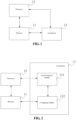
- FIG. 1 is a schematic diagram of an exemplary data computing system, according some embodiments of the present disclosure.
- the data computing system comprises a memory 11, a processor 12 and an accelerator 13.
- Memory 11 is communicatively coupled to processor 12 and configured to store data to be computed. All the data to be computed is written by processor 12 into memory 11.
- Processor 12 is communicatively coupled to accelerator 13 and configured to control accelerator 13.
- Accelerator 13 is communicatively coupled to memory 11 and configured to access memory 11 according to pre-configured control information, to implement data computing process, and to write a computed result back to memory 11.
- processor 12 of the data computing system when performing data computing process, controls accelerator 13 but does not perform the data computing process.
- the data computing process is completed by accelerator 13. Therefore, during the computing process, processor 12 does not need to access memory 11 and hence does not occupy the bus, thereby improving the utilization of the bus.
- accelerator 13 executes the data computing, processor 12 can process other events, and therefore the utilization of the processor is also improved.
- accelerator 13 can be coupled to any type of memory for computing.
- an experimental verification of wake-on-voice algorithm can be performed using some embodiments of the present disclosure.
- the experimental data result indicates that for the same wake-on-voice algorithm, the processing speed needs to be maintained at 196 MCPS (Millions of Cycles Per Second).
- the processing speed can reach 90 MCPS using accelerator 13. The performance can be improved by about 55%.
- FIG. 2 is a schematic diagram of an exemplary accelerator, according to some embodiments of the present disclosure.
- accelerator 13 includes control register module 131 and computing module 132.
- Control register module 131 is communicatively coupled to processor 12 and configured to store control information.
- the control information is pre-configured by processor 12 using a bus to deliver instructions.
- Computing module 132 is communicatively coupled to memory 11 and configured to access memory 11 according to the control information, to implement data computing, and to write a computed result back to memory 11.
- control information includes a start address for the data to be computed, the number of operands, a computing type, a write-back address for a computed result, and a computing enable flag.
- the computing type includes multiply-accumulate operation, exponential function, sigmoid function, rectifier (ReLU) function, and softmax function.
- computing module 132 can implement multiply-accumulate operations, exponential functions, sigmoid functions, rectifier (ReLU) functions, and softmax functions.
- the computing types of the present disclosure are not limited to the several types above, and the computing type can be customized according to actual requirements of a software application. During execution, the computing type can be controlled by the processor in such a manner that its use is flexible and convenient. Moreover, hardware implementations of the computing type can be added or deleted according to actual requirements in order to achieve the effect of optimizing the chip area.
- computing module 132 After detecting that the computing enable flag is 1, computing module 132 reads the data to be computed sequentially from memory 11 according to the start address for the data to be computed and the number of operands, and then performs data computing according to the computing type and writes a computed result back to memory 11 according to the write-back address for computed result. At the same time, computing module 132 resets the computing enable flag. After reading that the computing enable flag is 0, processor 12 can start the next computing or can read the computed result from memory 11.
- FIG. 3 is a schematic structural diagram of an exemplary computing module, according to some embodiments of the present disclosure.
- computing module 132 when implementing the multiply-accumulate operation or rectifier (ReLU) function, comprises a multiply-accumulate unit 1321, a rectifier (ReLU) computing unit 1322, a first multiplexer 1323 and a second multiplexer 1324.
- ReLU rectifier
- Multiply-accumulate unit 1321 comprises a 2-channel 16-bit multiplier 13211, a 2-channel 8-bit multiplier 13212, an accumulator 13214 and a register 13213.
- Multiply-accumulate unit 1321 is configured to perform parallel computing using 2-channel 16-bit multiplier 13211 and 2-channel 8-bit multiplier 13212, and store a multiply-accumulate computed result into register 13213.
- Rectifier (ReLU) computing unit 1322 is configured to perform rectifier (ReLU) function computing for input data 1320 or the multiply-accumulate computed result from multiply-accumulate unit 1321.
- First multiplexer 1323 is configured to select, according to signal ReLU_bypass, either the multiply-accumulate computed result from multiply-accumulate unit 1321 or input data 1320 as the data input to rectifier (ReLU) computing unit 1322.
- Second multiplexer 1324 is configured to select, according to signal ReLU_bypass, whether to perform rectifier (ReLU) function computing for the multiply-accumulate computed result from multiply-accumulate unit 1321.
- ReLU rectifier
- FIG. 4 is a diagram of an exemplary 32-channel 8 ⁇ 8 data storage format and computing process, according to some embodiments of the present disclosure. According to FIG. 4 , to perform a 32-channel 8 ⁇ 8 multiply-accumulate computing, the computing process is illustrated below.
- Processor 12 writes data A and data B into memory 11 through the bus, and no data is written until the subsequent computing process is completed. If the data to be computed needs to be replaced after the computing process is completed, processor 12 rewrites the data to be computed.
- processor 12 configures control register module 131 of accelerator 13, a start address for data A (DATA0_Start_addr), a start address for data B (DATA1_Start_addr), and a write-back address (Result_wb_addr) for a computed result.
- Processor 12 then configures the computing type to be the 32-channel 8 ⁇ 8 multiply-accumulate computing (e.g., the computing of FIG. 4 ), sets the number of operands to 32 and sets the computing enable flag to 1.
- the computing type e.g., the 32-channel 8 ⁇ 8 multiply-accumulate computing (e.g., the computing of FIG. 4 ), sets the number of operands to 32 and sets the computing enable flag to 1.
- computing module 132 of accelerator 13 After detecting that the computing enable flag is 1, computing module 132 of accelerator 13 starts the computing process, reads the data to be computed from memory 11 according to the start address for data A (DATA0_Start_addr), the start address for data B (DATA1_Start_addr) and the number of operands, and performs multiply-accumulate computing.
- the computed result is written back into memory 11 according to the write-back address (Result_wb_addr) , and the computing enable flag is reset.
- processor 12 After reading that the computing enable flag is 0, processor 12 can initiate the next computing process or read the computed result from memory 11.
- FIG. 5 is a diagram of an exemplary 4-channel 16 ⁇ 16 multiply-accumulate data storage format and computing process, according to some embodiments of the present disclosure. According to FIG. 5 , to perform a 4-channel 16 ⁇ 16 multiply-accumulate computing, the computing process is illustrated below.
- Processor 12 writes data A and data B into memory 11 through the bus, and no data is written until the subsequent computing process is completed. If the data to be computed needs to be replaced after the computing process is completed, processor 12 rewrites data to be computed.
- processor 12 configures control register module 131 of accelerator 13, a start address for data A (DATA0_Start_addr), a start address for data B (DATA1_Start_addr), and a write-back address (Result_wb_addr) for a computed result.
- Processor 12 then configures the computing type to be the 4-channel 16 ⁇ 16 multiply-accumulate computing (e.g., the computing of FIG. 5 ), sets the number of operands to 4 and sets the computing enable flag to 1.
- the computing type is the 4-channel 16 ⁇ 16 multiply-accumulate computing (e.g., the computing of FIG. 5 ), sets the number of operands to 4 and sets the computing enable flag to 1.
- computing module 132 of accelerator 13 After detecting that the computing enable flag is 1, computing module 132 of accelerator 13 starts the computing process, reads the data to be computed from memory 11 according to the start address for data A (DATA0_Start_addr), the start address for data B (DATA1_Start_addr) and the number of operands, and performs multiply-accumulate computing.
- the computed result is written back into memory 11 according to the write-back address (Result wb_addr), and the computing enable flag is reset.
- processor 12 After reading that the computing enable flag is 0, processor 12 can initiate the next computing process or read the computed result from memory 11.
- FIG. 6 is a diagram of an exemplary data storage formats and computing process for an exponential function, a softmax function, and a sigmoid function, according to some embodiments of the present disclosure.
- the computing process of FIG. 6 is similar to the multiply-accumulate computing processes of FIG.4 and FIG. 5 .
- processor 12 configures the computing type to be an exponential function, a softmax function, or a sigmoid function.
Landscapes
- Engineering & Computer Science (AREA)
- Theoretical Computer Science (AREA)
- Physics & Mathematics (AREA)
- General Physics & Mathematics (AREA)
- General Engineering & Computer Science (AREA)
- Computing Systems (AREA)
- Pure & Applied Mathematics (AREA)
- Mathematical Analysis (AREA)
- Computational Mathematics (AREA)
- Mathematical Optimization (AREA)
- Software Systems (AREA)
- Health & Medical Sciences (AREA)
- Life Sciences & Earth Sciences (AREA)
- Biomedical Technology (AREA)
- Biophysics (AREA)
- Computational Linguistics (AREA)
- Mathematical Physics (AREA)
- Artificial Intelligence (AREA)
- Evolutionary Computation (AREA)
- Data Mining & Analysis (AREA)
- Molecular Biology (AREA)
- General Health & Medical Sciences (AREA)
- Human Computer Interaction (AREA)
- Neurology (AREA)
- Computer Hardware Design (AREA)
- Advance Control (AREA)
- Multi Processors (AREA)
- Complex Calculations (AREA)
Applications Claiming Priority (3)
| Application Number | Priority Date | Filing Date | Title |
|---|---|---|---|
| CN201810235312.9A CN108446096B (zh) | 2018-03-21 | 2018-03-21 | 数据计算系统 |
| PCT/CN2019/077132 WO2019179311A1 (en) | 2018-03-21 | 2019-03-06 | Data computing system |
| EP19771895.0A EP3765956B1 (de) | 2018-03-21 | 2019-03-06 | Datenverarbeitungssystem |
Related Parent Applications (1)
| Application Number | Title | Priority Date | Filing Date |
|---|---|---|---|
| EP19771895.0A Division EP3765956B1 (de) | 2018-03-21 | 2019-03-06 | Datenverarbeitungssystem |
Publications (3)
| Publication Number | Publication Date |
|---|---|
| EP4404055A2 true EP4404055A2 (de) | 2024-07-24 |
| EP4404055A3 EP4404055A3 (de) | 2024-10-16 |
| EP4404055B1 EP4404055B1 (de) | 2025-11-12 |
Family
ID=63196016
Family Applications (2)
| Application Number | Title | Priority Date | Filing Date |
|---|---|---|---|
| EP24181514.1A Active EP4404055B1 (de) | 2018-03-21 | 2019-03-06 | Datenverarbeitungssystem |
| EP19771895.0A Active EP3765956B1 (de) | 2018-03-21 | 2019-03-06 | Datenverarbeitungssystem |
Family Applications After (1)
| Application Number | Title | Priority Date | Filing Date |
|---|---|---|---|
| EP19771895.0A Active EP3765956B1 (de) | 2018-03-21 | 2019-03-06 | Datenverarbeitungssystem |
Country Status (5)
| Country | Link |
|---|---|
| US (3) | US11243771B2 (de) |
| EP (2) | EP4404055B1 (de) |
| JP (2) | JP7381481B2 (de) |
| CN (1) | CN108446096B (de) |
| WO (1) | WO2019179311A1 (de) |
Families Citing this family (3)
| Publication number | Priority date | Publication date | Assignee | Title |
|---|---|---|---|---|
| CN108446096B (zh) * | 2018-03-21 | 2021-01-29 | 杭州中天微系统有限公司 | 数据计算系统 |
| CN110245096B (zh) * | 2019-06-24 | 2023-07-25 | 苏州暴雪电子科技有限公司 | 一种实现处理器直接连接扩展计算模块的方法 |
| CN112541581A (zh) * | 2019-09-23 | 2021-03-23 | 阿里巴巴集团控股有限公司 | 一种加速计算单元和加速计算系统 |
Family Cites Families (31)
| Publication number | Priority date | Publication date | Assignee | Title |
|---|---|---|---|---|
| JPH04104358A (ja) | 1990-08-23 | 1992-04-06 | Hitachi Ltd | マイクロコンピュータ装置 |
| US5742839A (en) * | 1992-01-30 | 1998-04-21 | Fujitsu Limited | Coprocessor for performing an arithmetic operation by automatically reading data from an external memory |
| JPH10187599A (ja) * | 1996-11-07 | 1998-07-21 | Yamaha Corp | デジタル信号処理装置 |
| EP0945788B1 (de) * | 1998-02-04 | 2004-08-04 | Texas Instruments Inc. | Datenverarbeitungssytem mit einem digitalen Signalprozessor und einem Koprozessor und Datenverarbeitungsverfahren |
| US6219764B1 (en) * | 1998-08-03 | 2001-04-17 | Micron Technology, Inc. | Memory paging control method |
| US6526430B1 (en) | 1999-10-04 | 2003-02-25 | Texas Instruments Incorporated | Reconfigurable SIMD coprocessor architecture for sum of absolute differences and symmetric filtering (scalable MAC engine for image processing) |
| JP3710798B2 (ja) * | 2003-09-12 | 2005-10-26 | 松下電器産業株式会社 | 複合演算処理装置 |
| CN101782930B (zh) | 2009-01-21 | 2012-08-22 | 国际商业机器公司 | 在多处理器系统上进行分子动力学模拟的方法和装置 |
| WO2010150474A1 (ja) | 2009-06-23 | 2010-12-29 | セイコーエプソン株式会社 | サブプロセッサー、集積回路装置及び電子機器 |
| CN102122275A (zh) * | 2010-01-08 | 2011-07-13 | 上海芯豪微电子有限公司 | 一种可配置处理器 |
| CN101794210A (zh) * | 2010-04-07 | 2010-08-04 | 上海交通大学 | 基于fpga的通用矩阵浮点乘法器 |
| US10157060B2 (en) * | 2011-12-29 | 2018-12-18 | Intel Corporation | Method, device and system for control signaling in a data path module of a data stream processing engine |
| US9460144B2 (en) * | 2012-01-13 | 2016-10-04 | Oracle International Corporation | Lock acceleration |
| US20150032922A1 (en) | 2012-02-28 | 2015-01-29 | Nec Corporation | Computer system, method of processing the same, and computer readble medium |
| US9814037B2 (en) * | 2013-06-28 | 2017-11-07 | Intel Corporation | Method for efficient channel estimation and beamforming in FDD system by exploiting uplink-downlink correspondence |
| DE102013212842A1 (de) * | 2013-07-02 | 2015-01-08 | Robert Bosch Gmbh | Verfahren zum Betreiben eines Steuergeräts sowie Steuergerät mit einer Modellberechnungseinheit |
| US9785444B2 (en) * | 2013-08-16 | 2017-10-10 | Analog Devices Global | Hardware accelerator configuration by a translation of configuration data |
| CN103677739B (zh) * | 2013-11-28 | 2016-08-17 | 中国航天科技集团公司第九研究院第七七一研究所 | 一种可配置的乘累加运算单元及其构成的乘累加运算阵列 |
| US9122514B2 (en) * | 2014-01-07 | 2015-09-01 | International Business Machines Corporation | Administering message acknowledgements in a parallel computer |
| US20180046903A1 (en) * | 2016-08-12 | 2018-02-15 | DeePhi Technology Co., Ltd. | Deep processing unit (dpu) for implementing an artificial neural network (ann) |
| CN107688469B (zh) | 2016-12-23 | 2020-02-11 | 北京国睿中数科技股份有限公司 | 兼顾通用指令和专用指令的可重构计算装置 |
| US10402527B2 (en) * | 2017-01-04 | 2019-09-03 | Stmicroelectronics S.R.L. | Reconfigurable interconnect |
| CA3108151C (en) * | 2017-02-23 | 2024-02-20 | Cerebras Systems Inc. | Accelerated deep learning |
| US10186011B2 (en) * | 2017-04-28 | 2019-01-22 | Intel Corporation | Programmable coarse grained and sparse matrix compute hardware with advanced scheduling |
| US11775313B2 (en) * | 2017-05-26 | 2023-10-03 | Purdue Research Foundation | Hardware accelerator for convolutional neural networks and method of operation thereof |
| CN107391447A (zh) * | 2017-07-26 | 2017-11-24 | 成都网烁信息科技有限公司 | 一种电脑加速系统及方法 |
| CN107527090A (zh) | 2017-08-24 | 2017-12-29 | 中国科学院计算技术研究所 | 应用于稀疏神经网络的处理器和处理方法 |
| CN107622305A (zh) | 2017-08-24 | 2018-01-23 | 中国科学院计算技术研究所 | 用于神经网络的处理器和处理方法 |
| US11222256B2 (en) * | 2017-10-17 | 2022-01-11 | Xilinx, Inc. | Neural network processing system having multiple processors and a neural network accelerator |
| CN108701015A (zh) * | 2017-11-30 | 2018-10-23 | 深圳市大疆创新科技有限公司 | 用于神经网络的运算装置、芯片、设备及相关方法 |
| CN108446096B (zh) | 2018-03-21 | 2021-01-29 | 杭州中天微系统有限公司 | 数据计算系统 |
-
2018
- 2018-03-21 CN CN201810235312.9A patent/CN108446096B/zh active Active
-
2019
- 2019-03-06 WO PCT/CN2019/077132 patent/WO2019179311A1/en not_active Ceased
- 2019-03-06 EP EP24181514.1A patent/EP4404055B1/de active Active
- 2019-03-06 JP JP2020546455A patent/JP7381481B2/ja active Active
- 2019-03-06 US US16/479,320 patent/US11243771B2/en active Active
- 2019-03-06 EP EP19771895.0A patent/EP3765956B1/de active Active
-
2022
- 2022-01-21 US US17/648,659 patent/US11972262B2/en active Active
-
2023
- 2023-11-02 JP JP2023188892A patent/JP7696408B2/ja active Active
-
2024
- 2024-04-02 US US18/624,870 patent/US20240264836A1/en active Pending
Also Published As
| Publication number | Publication date |
|---|---|
| US20220147357A1 (en) | 2022-05-12 |
| WO2019179311A1 (en) | 2019-09-26 |
| JP2021517299A (ja) | 2021-07-15 |
| US11972262B2 (en) | 2024-04-30 |
| JP7381481B2 (ja) | 2023-11-15 |
| US20210055879A1 (en) | 2021-02-25 |
| JP2024003111A (ja) | 2024-01-11 |
| CN108446096B (zh) | 2021-01-29 |
| EP3765956A1 (de) | 2021-01-20 |
| US20240264836A1 (en) | 2024-08-08 |
| EP4404055B1 (de) | 2025-11-12 |
| EP4404055A3 (de) | 2024-10-16 |
| EP3765956B1 (de) | 2024-07-03 |
| US11243771B2 (en) | 2022-02-08 |
| CN108446096A (zh) | 2018-08-24 |
| EP3765956A4 (de) | 2021-04-28 |
| JP7696408B2 (ja) | 2025-06-20 |
Similar Documents
| Publication | Publication Date | Title |
|---|---|---|
| US20240264836A1 (en) | Data computing system | |
| CN107766079B (zh) | 处理器以及用于在处理器上执行指令的方法 | |
| CN108733578A (zh) | 快闪存储器的垃圾回收断电回复方法及使用该方法的装置 | |
| CN111813703B (zh) | 数据储存装置及逻辑至物理地址映射表的更新方法 | |
| CN112214158A (zh) | 主机输出输入命令的执行装置及方法及计算机可读取存储介质 | |
| US11960396B2 (en) | Method and computer program product for performing data writes into a flash memory | |
| CN111796759B (zh) | 多平面上的片段数据读取的计算机可读取存储介质及方法 | |
| EP2927779A1 (de) | Plattenschreibverfahren für speicherplattenanordnungen und plattenschreibvorrichtung für speicherplattenanordnungen | |
| CN111047037B (zh) | 数据处理方法、装置、设备及存储介质 | |
| CN115933994B (zh) | 一种数据处理方法、装置、电子设备及存储介质 | |
| KR102454695B1 (ko) | 캐시 장치, 캐시, 시스템, 데이터 처리 방법, 장치 및 매체 | |
| WO2025152506A1 (zh) | 一种数据处理系统、方法、设备及非易失性可读存储介质 | |
| KR20080105390A (ko) | 플래시 메모리에 사용되는 명령어들을 제어하는 방법 및장치 | |
| CN112214095A (zh) | 一种控制硬盘功耗的方法和设备 | |
| US8145822B2 (en) | Computer system for electronic data processing | |
| CN108932209B (zh) | 存储器装置及其操作方法 | |
| CN116661704B (zh) | 存储装置数据读写方法、存储器存储装置及存储器控制器 | |
| CN108170380B (zh) | 一种固态硬盘提升顺序读性能的方法及固态硬盘 | |
| US10521156B2 (en) | Apparatus and method of managing multi solid state disk system | |
| CN109935252B (zh) | 存储器装置及其操作方法 | |
| EP2434409B1 (de) | Prozessor und Verfahren dafür | |
| US11029881B2 (en) | Memory controller, memory system, and information processing system | |
| US10566062B2 (en) | Memory device and method for operating the same | |
| SU608160A1 (ru) | Центральный процессор | |
| JPS59200345A (ja) | マイクロプログラム制御方式 |
Legal Events
| Date | Code | Title | Description |
|---|---|---|---|
| PUAI | Public reference made under article 153(3) epc to a published international application that has entered the european phase |
Free format text: ORIGINAL CODE: 0009012 |
|
| STAA | Information on the status of an ep patent application or granted ep patent |
Free format text: STATUS: THE APPLICATION HAS BEEN PUBLISHED |
|
| AC | Divisional application: reference to earlier application |
Ref document number: 3765956 Country of ref document: EP Kind code of ref document: P |
|
| AK | Designated contracting states |
Kind code of ref document: A2 Designated state(s): AL AT BE BG CH CY CZ DE DK EE ES FI FR GB GR HR HU IE IS IT LI LT LU LV MC MK MT NL NO PL PT RO RS SE SI SK SM TR |
|
| REG | Reference to a national code |
Ref country code: DE Ref legal event code: R079 Free format text: PREVIOUS MAIN CLASS: G06F0009380000 Ipc: G06F0007498000 Ref country code: DE Ref legal event code: R079 Ref document number: 602019078180 Country of ref document: DE Free format text: PREVIOUS MAIN CLASS: G06F0009380000 Ipc: G06F0007498000 |
|
| PUAL | Search report despatched |
Free format text: ORIGINAL CODE: 0009013 |
|
| AK | Designated contracting states |
Kind code of ref document: A3 Designated state(s): AL AT BE BG CH CY CZ DE DK EE ES FI FR GB GR HR HU IE IS IT LI LT LU LV MC MK MT NL NO PL PT RO RS SE SI SK SM TR |
|
| RIC1 | Information provided on ipc code assigned before grant |
Ipc: G06F 9/38 20180101ALI20240910BHEP Ipc: G06F 7/57 20060101ALI20240910BHEP Ipc: G06N 3/063 20230101ALI20240910BHEP Ipc: G06F 7/498 20060101AFI20240910BHEP |
|
| STAA | Information on the status of an ep patent application or granted ep patent |
Free format text: STATUS: REQUEST FOR EXAMINATION WAS MADE |
|
| 17P | Request for examination filed |
Effective date: 20250409 |
|
| GRAP | Despatch of communication of intention to grant a patent |
Free format text: ORIGINAL CODE: EPIDOSNIGR1 |
|
| STAA | Information on the status of an ep patent application or granted ep patent |
Free format text: STATUS: GRANT OF PATENT IS INTENDED |
|
| INTG | Intention to grant announced |
Effective date: 20250603 |
|
| GRAS | Grant fee paid |
Free format text: ORIGINAL CODE: EPIDOSNIGR3 |
|
| GRAA | (expected) grant |
Free format text: ORIGINAL CODE: 0009210 |
|
| STAA | Information on the status of an ep patent application or granted ep patent |
Free format text: STATUS: THE PATENT HAS BEEN GRANTED |
|
| AC | Divisional application: reference to earlier application |
Ref document number: 3765956 Country of ref document: EP Kind code of ref document: P |
|
| AK | Designated contracting states |
Kind code of ref document: B1 Designated state(s): AL AT BE BG CH CY CZ DE DK EE ES FI FR GB GR HR HU IE IS IT LI LT LU LV MC MK MT NL NO PL PT RO RS SE SI SK SM TR |
|
| REG | Reference to a national code |
Ref country code: CH Ref legal event code: F10 Free format text: ST27 STATUS EVENT CODE: U-0-0-F10-F00 (AS PROVIDED BY THE NATIONAL OFFICE) Effective date: 20251112 Ref country code: GB Ref legal event code: FG4D |
|
| REG | Reference to a national code |
Ref country code: IE Ref legal event code: FG4D |
|
| REG | Reference to a national code |
Ref country code: DE Ref legal event code: R096 Ref document number: 602019078180 Country of ref document: DE |
|
| REG | Reference to a national code |
Ref country code: NL Ref legal event code: MP Effective date: 20251112 |
|
| PGFP | Annual fee paid to national office [announced via postgrant information from national office to epo] |
Ref country code: GB Payment date: 20260325 Year of fee payment: 8 |
|
| PG25 | Lapsed in a contracting state [announced via postgrant information from national office to epo] |
Ref country code: ES Free format text: LAPSE BECAUSE OF FAILURE TO SUBMIT A TRANSLATION OF THE DESCRIPTION OR TO PAY THE FEE WITHIN THE PRESCRIBED TIME-LIMIT Effective date: 20251112 |
|
| REG | Reference to a national code |
Ref country code: LT Ref legal event code: MG9D |
|
| PG25 | Lapsed in a contracting state [announced via postgrant information from national office to epo] |
Ref country code: NO Free format text: LAPSE BECAUSE OF FAILURE TO SUBMIT A TRANSLATION OF THE DESCRIPTION OR TO PAY THE FEE WITHIN THE PRESCRIBED TIME-LIMIT Effective date: 20260212 |
|
| PGFP | Annual fee paid to national office [announced via postgrant information from national office to epo] |
Ref country code: DE Payment date: 20260324 Year of fee payment: 8 |
|
| PG25 | Lapsed in a contracting state [announced via postgrant information from national office to epo] |
Ref country code: HR Free format text: LAPSE BECAUSE OF FAILURE TO SUBMIT A TRANSLATION OF THE DESCRIPTION OR TO PAY THE FEE WITHIN THE PRESCRIBED TIME-LIMIT Effective date: 20251112 Ref country code: AT Free format text: LAPSE BECAUSE OF FAILURE TO SUBMIT A TRANSLATION OF THE DESCRIPTION OR TO PAY THE FEE WITHIN THE PRESCRIBED TIME-LIMIT Effective date: 20251112 Ref country code: FI Free format text: LAPSE BECAUSE OF FAILURE TO SUBMIT A TRANSLATION OF THE DESCRIPTION OR TO PAY THE FEE WITHIN THE PRESCRIBED TIME-LIMIT Effective date: 20251112 |
|
| REG | Reference to a national code |
Ref country code: AT Ref legal event code: MK05 Ref document number: 1857310 Country of ref document: AT Kind code of ref document: T Effective date: 20251112 |
|
| PG25 | Lapsed in a contracting state [announced via postgrant information from national office to epo] |
Ref country code: NL Free format text: LAPSE BECAUSE OF FAILURE TO SUBMIT A TRANSLATION OF THE DESCRIPTION OR TO PAY THE FEE WITHIN THE PRESCRIBED TIME-LIMIT Effective date: 20251112 |
|
| PG25 | Lapsed in a contracting state [announced via postgrant information from national office to epo] |
Ref country code: RS Free format text: LAPSE BECAUSE OF FAILURE TO SUBMIT A TRANSLATION OF THE DESCRIPTION OR TO PAY THE FEE WITHIN THE PRESCRIBED TIME-LIMIT Effective date: 20260212 |
|
| PG25 | Lapsed in a contracting state [announced via postgrant information from national office to epo] |
Ref country code: IS Free format text: LAPSE BECAUSE OF FAILURE TO SUBMIT A TRANSLATION OF THE DESCRIPTION OR TO PAY THE FEE WITHIN THE PRESCRIBED TIME-LIMIT Effective date: 20260312 |
|
| PGFP | Annual fee paid to national office [announced via postgrant information from national office to epo] |
Ref country code: FR Payment date: 20260330 Year of fee payment: 8 |
|
| PG25 | Lapsed in a contracting state [announced via postgrant information from national office to epo] |
Ref country code: PT Free format text: LAPSE BECAUSE OF FAILURE TO SUBMIT A TRANSLATION OF THE DESCRIPTION OR TO PAY THE FEE WITHIN THE PRESCRIBED TIME-LIMIT Effective date: 20260312 |
|
| PG25 | Lapsed in a contracting state [announced via postgrant information from national office to epo] |
Ref country code: PL Free format text: LAPSE BECAUSE OF FAILURE TO SUBMIT A TRANSLATION OF THE DESCRIPTION OR TO PAY THE FEE WITHIN THE PRESCRIBED TIME-LIMIT Effective date: 20251112 |
|
| PG25 | Lapsed in a contracting state [announced via postgrant information from national office to epo] |
Ref country code: LV Free format text: LAPSE BECAUSE OF FAILURE TO SUBMIT A TRANSLATION OF THE DESCRIPTION OR TO PAY THE FEE WITHIN THE PRESCRIBED TIME-LIMIT Effective date: 20251112 |