EP4394829A2 - Mehrschichtiges elektronisches bauteil - Google Patents
Mehrschichtiges elektronisches bauteil Download PDFInfo
- Publication number
- EP4394829A2 EP4394829A2 EP23201804.4A EP23201804A EP4394829A2 EP 4394829 A2 EP4394829 A2 EP 4394829A2 EP 23201804 A EP23201804 A EP 23201804A EP 4394829 A2 EP4394829 A2 EP 4394829A2
- Authority
- EP
- European Patent Office
- Prior art keywords
- plating layer
- layer
- resin
- component
- electrode
- Prior art date
- Legal status (The legal status is an assumption and is not a legal conclusion. Google has not performed a legal analysis and makes no representation as to the accuracy of the status listed.)
- Pending
Links
Images




Classifications
-
- H—ELECTRICITY
- H01—ELECTRIC ELEMENTS
- H01G—CAPACITORS; CAPACITORS, RECTIFIERS, DETECTORS, SWITCHING DEVICES, LIGHT-SENSITIVE OR TEMPERATURE-SENSITIVE DEVICES OF THE ELECTROLYTIC TYPE
- H01G4/00—Fixed capacitors; Processes of their manufacture
- H01G4/002—Details
- H01G4/018—Dielectrics
- H01G4/06—Solid dielectrics
- H01G4/08—Inorganic dielectrics
- H01G4/12—Ceramic dielectrics
- H01G4/1209—Ceramic dielectrics characterised by the ceramic dielectric material
- H01G4/1218—Ceramic dielectrics characterised by the ceramic dielectric material based on titanium oxides or titanates
- H01G4/1227—Ceramic dielectrics characterised by the ceramic dielectric material based on titanium oxides or titanates based on alkaline earth titanates
-
- H—ELECTRICITY
- H01—ELECTRIC ELEMENTS
- H01G—CAPACITORS; CAPACITORS, RECTIFIERS, DETECTORS, SWITCHING DEVICES, LIGHT-SENSITIVE OR TEMPERATURE-SENSITIVE DEVICES OF THE ELECTROLYTIC TYPE
- H01G4/00—Fixed capacitors; Processes of their manufacture
- H01G4/30—Stacked capacitors
-
- H—ELECTRICITY
- H01—ELECTRIC ELEMENTS
- H01G—CAPACITORS; CAPACITORS, RECTIFIERS, DETECTORS, SWITCHING DEVICES, LIGHT-SENSITIVE OR TEMPERATURE-SENSITIVE DEVICES OF THE ELECTROLYTIC TYPE
- H01G4/00—Fixed capacitors; Processes of their manufacture
- H01G4/002—Details
- H01G4/005—Electrodes
- H01G4/008—Selection of materials
-
- H—ELECTRICITY
- H01—ELECTRIC ELEMENTS
- H01G—CAPACITORS; CAPACITORS, RECTIFIERS, DETECTORS, SWITCHING DEVICES, LIGHT-SENSITIVE OR TEMPERATURE-SENSITIVE DEVICES OF THE ELECTROLYTIC TYPE
- H01G4/00—Fixed capacitors; Processes of their manufacture
- H01G4/002—Details
- H01G4/005—Electrodes
- H01G4/012—Form of non-self-supporting electrodes
-
- H—ELECTRICITY
- H01—ELECTRIC ELEMENTS
- H01G—CAPACITORS; CAPACITORS, RECTIFIERS, DETECTORS, SWITCHING DEVICES, LIGHT-SENSITIVE OR TEMPERATURE-SENSITIVE DEVICES OF THE ELECTROLYTIC TYPE
- H01G4/00—Fixed capacitors; Processes of their manufacture
- H01G4/002—Details
- H01G4/228—Terminals
- H01G4/232—Terminals electrically connecting two or more layers of a stacked or rolled capacitor
-
- H—ELECTRICITY
- H01—ELECTRIC ELEMENTS
- H01G—CAPACITORS; CAPACITORS, RECTIFIERS, DETECTORS, SWITCHING DEVICES, LIGHT-SENSITIVE OR TEMPERATURE-SENSITIVE DEVICES OF THE ELECTROLYTIC TYPE
- H01G4/00—Fixed capacitors; Processes of their manufacture
- H01G4/002—Details
- H01G4/228—Terminals
- H01G4/232—Terminals electrically connecting two or more layers of a stacked or rolled capacitor
- H01G4/2325—Terminals electrically connecting two or more layers of a stacked or rolled capacitor characterised by the material of the terminals
-
- H—ELECTRICITY
- H01—ELECTRIC ELEMENTS
- H01G—CAPACITORS; CAPACITORS, RECTIFIERS, DETECTORS, SWITCHING DEVICES, LIGHT-SENSITIVE OR TEMPERATURE-SENSITIVE DEVICES OF THE ELECTROLYTIC TYPE
- H01G4/00—Fixed capacitors; Processes of their manufacture
- H01G4/002—Details
- H01G4/018—Dielectrics
- H01G4/06—Solid dielectrics
- H01G4/08—Inorganic dielectrics
- H01G4/12—Ceramic dielectrics
Definitions
- the barium titanate-based material may include barium titanate (BaTiO 3 )-based ceramic powders, and the ceramic powders may be, for example, BaTiO 3 or (Ba 1-x Ca x )TiO 3 (0 ⁇ x ⁇ 1), Ba(Ti 1-y Ca y )O 3 (0 ⁇ y ⁇ 1), (Ba 1-x Ca x )(Ti 1-y Zr y )O 3 (0 ⁇ x ⁇ 1, 0 ⁇ y ⁇ 1) or Ba(Ti 1-y Zr y )O 3 (0 ⁇ y ⁇ 1), in which calcium (Ca), zirconium (Zr) or the like is partially dissolved in BaTiO 3 .
- BaTiO 3 barium titanate
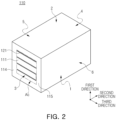
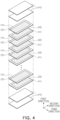
- the capacitance formation part Ac may be a part that contributes to forming the capacitance of the capacitor, and formed by repeatedly stacking the plurality of first and second internal electrodes 121 and 122 on each other while having the dielectric layer 111 interposed therebetween.
- a marginal part 114 or 115 may be positioned on one surface or the other surface of the capacitance formation part Ac in the third direction.
- the marginal part 114 or 115 may indicate a region between each of two ends of the first or second internal electrode 121 or 122 and a boundary surface of the body 110.
- the body 110 may be formed by alternately stacking the ceramic green sheet on which the first internal electrode 121 is printed and the ceramic green sheet on which the second internal electrode 122 is printed on each other and then sintering the same.
- the description describes a structure of the external electrode 130 or 140 based on the first external electrode 130. Descriptions of the first external electrode 130 may also be applied to the second external electrode 140.
- a prior art suggests a method of performing heat treatment by forming a tin (Sn) plating layer on the nickel (Ni) plating layer and then forming an appropriate hole in the tin (Sn) plating layer to remove hydrogen occurring during the process of forming the plating layer and absorbed in the nickel (Ni) plating layer.
- the tin (Sn) plating layer has a 100 times lower diffusion coefficient for hydrogen than the nickel (Ni) plating layer. Accordingly, there is a limit to removing hydrogen already absorbed in the nickel (Ni) plating layer, and solderability of the multilayer electronic component may be deteriorated in the case of forming such a separate hole in the tin (Sn) plating layer.
- the first plating layer 132 may be formed using electrolytic plating, is not limited thereto, and may also be formed by wet plating such as electroless plating or dry plating such as sputtering or deposition. These plating methods may also be applied to the second plating layer 133 and a third plating layer 135 to be described below.
- a ratio of the average thickness t1 of the first plating layer 132 to the average thickness t2 of the second plating layer 133 may be 0.9 or less. In this manner, it is possible to effectively remove hydrogen permeating into the body 110 or the electrode layer 131 through the heat treatment performed after the first plating layer 132 is formed, and to improve the high temperature reliability and moisture resistance reliability of the multilayer electronic component 100.
- the multilayer electronic component 100 may be polished to its center in the third direction to expose the cross sections in the first and second directions, and the first external electrode 130 may then be observed using the scanning electron microscope (SEM) or the optical microscope (OM). The measurement may be performed at a center of a region in the first direction of the first plating layer 132 or the second plating layer 133, positioned on the third surface 3 of the body 110.
- SEM scanning electron microscope
- OM optical microscope
- the oxide 134 including nickel (Ni) may include nickel oxide such as NiO or Ni 2 O 3 , and may include nickel hydroxide such as Ni(OH) 2 .
- the second plating layer 133 including nickel (Ni) may be positioned on the oxide 134 including nickel (Ni), and the heat treatment for removing hydrogen may proceed after the first plating layer 132 is formed. Therefore, the oxide 134 including nickel (Ni) may be NiO.
- the electrode layer 131 may further include glass.
- the electrode layer 131 is a component positioned on the third surface 3 or the fourth surface 4 of the body 110, and may be in contact with one surface of the body 110.
- the electrode layer 131 may be difficult to secure adhesion with the body 110 that uses a dielectric ceramic as its main element.
- the electrode layer 131 may improve adhesion between the body 110 and the external electrode 130.
- a boundary surface resistance thereof may be greater than that of a sintered electrode including glass. Therefore, it is highly likely that excessive hydrogen occurs in an initial stage of forming the first plating layer 132 on the electrode layer 131 as the plating layer.
- Test nos. 1 and 2 are cases where the average thickness t1 of the first plating layer is 0.9 um or less, and the reliability of the multilayer electronic component is improved when the heat treatment according to the present disclosure is performed thereon, and the improved reliability is seen to be caused by effectively removing hydrogen permeating into the body 110 or the electrode layer 131 when the heat treatment according to the present disclosure is performed.
- the present disclosure may provide the multilayer electronic component which may suppress the permeation of hydrogen into the internal electrode or the dielectric layer in the process of forming the plating layer on the external electrode.
- the present disclosure may provide the multilayer electronic component which may secure its reliability by effectively removing hydrogen permeating into the internal electrode or the dielectric layer in the process of forming the plating layer on the external electrode.
Landscapes
- Engineering & Computer Science (AREA)
- Power Engineering (AREA)
- Manufacturing & Machinery (AREA)
- Microelectronics & Electronic Packaging (AREA)
- Chemical & Material Sciences (AREA)
- Ceramic Engineering (AREA)
- Inorganic Chemistry (AREA)
- Materials Engineering (AREA)
- Fixed Capacitors And Capacitor Manufacturing Machines (AREA)
- Ceramic Capacitors (AREA)
Applications Claiming Priority (1)
| Application Number | Priority Date | Filing Date | Title |
|---|---|---|---|
| KR1020220190746A KR20240107780A (ko) | 2022-12-30 | 2022-12-30 | 적층형 전자 부품 |
Publications (2)
| Publication Number | Publication Date |
|---|---|
| EP4394829A2 true EP4394829A2 (de) | 2024-07-03 |
| EP4394829A3 EP4394829A3 (de) | 2025-01-15 |
Family
ID=88291063
Family Applications (1)
| Application Number | Title | Priority Date | Filing Date |
|---|---|---|---|
| EP23201804.4A Pending EP4394829A3 (de) | 2022-12-30 | 2023-10-05 | Mehrschichtiges elektronisches bauteil |
Country Status (5)
| Country | Link |
|---|---|
| US (1) | US12597566B2 (de) |
| EP (1) | EP4394829A3 (de) |
| JP (1) | JP2024095967A (de) |
| KR (1) | KR20240107780A (de) |
| CN (1) | CN118280730A (de) |
Family Cites Families (8)
| Publication number | Priority date | Publication date | Assignee | Title |
|---|---|---|---|---|
| JP3861927B1 (ja) | 2005-07-07 | 2006-12-27 | 株式会社村田製作所 | 電子部品、電子部品の実装構造および電子部品の製造方法 |
| JP5853627B2 (ja) | 2011-11-21 | 2016-02-09 | Tdk株式会社 | 電子部品 |
| KR20130111000A (ko) | 2012-03-30 | 2013-10-10 | 삼성전기주식회사 | 적층 세라믹 전자부품 및 이의 제조방법 |
| KR102142519B1 (ko) | 2018-06-29 | 2020-08-07 | 삼성전기주식회사 | 적층 세라믹 커패시터 |
| JP7088134B2 (ja) * | 2019-07-17 | 2022-06-21 | 株式会社村田製作所 | 電子部品 |
| JP7226161B2 (ja) | 2019-07-17 | 2023-02-21 | 株式会社村田製作所 | 電子部品 |
| JP7188356B2 (ja) | 2019-10-25 | 2022-12-13 | 株式会社村田製作所 | セラミック電子部品およびセラミック電子部品の製造方法 |
| JP2021182585A (ja) | 2020-05-19 | 2021-11-25 | 太陽誘電株式会社 | 積層セラミック電子部品の製造方法、積層セラミック電子部品及び回路基板 |
-
2022
- 2022-12-30 KR KR1020220190746A patent/KR20240107780A/ko active Pending
-
2023
- 2023-09-26 US US18/372,870 patent/US12597566B2/en active Active
- 2023-10-05 EP EP23201804.4A patent/EP4394829A3/de active Pending
- 2023-10-06 JP JP2023174385A patent/JP2024095967A/ja active Pending
- 2023-12-21 CN CN202311775753.5A patent/CN118280730A/zh active Pending
Also Published As
| Publication number | Publication date |
|---|---|
| EP4394829A3 (de) | 2025-01-15 |
| KR20240107780A (ko) | 2024-07-09 |
| CN118280730A (zh) | 2024-07-02 |
| US12597566B2 (en) | 2026-04-07 |
| US20240222030A1 (en) | 2024-07-04 |
| JP2024095967A (ja) | 2024-07-11 |
Similar Documents
| Publication | Publication Date | Title |
|---|---|---|
| CN108461292B (zh) | 多层陶瓷电容器 | |
| KR101751079B1 (ko) | 적층 세라믹 전자부품 및 이의 제조방법 | |
| US11587735B2 (en) | Multilayer electronic component and manufacturing method thereof | |
| US12142437B2 (en) | Multilayer ceramic capacitor | |
| US20240177934A1 (en) | Multilayer electronic component | |
| JP7803024B2 (ja) | 積層型電子部品 | |
| EP4379762A1 (de) | Mehrschichtiges elektronisches bauelement (mlcc) verbesserte schnittstelle mit externen elektroden | |
| US20250157739A1 (en) | Multilayer electronic component | |
| EP4394829A2 (de) | Mehrschichtiges elektronisches bauteil | |
| US20240312713A1 (en) | Multilayer electronic component | |
| EP4394828A2 (de) | Mehrschichtiges elektronisches bauteil | |
| US12456579B2 (en) | Multilayer electronic component | |
| EP4411765A2 (de) | Doppelte dielektrische deckschichten mit fluor für ein keramisches mehrschichtbauteil | |
| US12374497B2 (en) | Multilayer electronic component with improved reliability | |
| US11961681B2 (en) | Multilayer capacitor including internal electrodes having pores on ends thereof and board having the same mounted thereon | |
| US12469643B2 (en) | Multilayer electronic component | |
| EP4293691B1 (de) | Keramischer mehrschichtkondensator (mlcc) | |
| EP4386793A2 (de) | Mehrschichtiges elektronisches bauteil | |
| US12387876B2 (en) | Multilayer electronic component | |
| US20250157742A1 (en) | Multilayer electronic component | |
| US20260058061A1 (en) | Multilayer ceramic capacitor and method for manufacturing multilayer ceramic capacitor | |
| EP4421835A1 (de) | Vielschichtkondensator und verfahren zu seiner herstellung | |
| US20250157737A1 (en) | Multilayer electronic component | |
| KR102894855B1 (ko) | 적층형 커패시터 |
Legal Events
| Date | Code | Title | Description |
|---|---|---|---|
| PUAI | Public reference made under article 153(3) epc to a published international application that has entered the european phase |
Free format text: ORIGINAL CODE: 0009012 |
|
| STAA | Information on the status of an ep patent application or granted ep patent |
Free format text: STATUS: THE APPLICATION HAS BEEN PUBLISHED |
|
| AK | Designated contracting states |
Kind code of ref document: A2 Designated state(s): AL AT BE BG CH CY CZ DE DK EE ES FI FR GB GR HR HU IE IS IT LI LT LU LV MC ME MK MT NL NO PL PT RO RS SE SI SK SM TR |
|
| PUAL | Search report despatched |
Free format text: ORIGINAL CODE: 0009013 |
|
| AK | Designated contracting states |
Kind code of ref document: A3 Designated state(s): AL AT BE BG CH CY CZ DE DK EE ES FI FR GB GR HR HU IE IS IT LI LT LU LV MC ME MK MT NL NO PL PT RO RS SE SI SK SM TR |
|
| RIC1 | Information provided on ipc code assigned before grant |
Ipc: H01G 4/12 20060101ALN20241212BHEP Ipc: H01G 4/30 20060101ALI20241212BHEP Ipc: H01G 4/232 20060101AFI20241212BHEP |
|
| STAA | Information on the status of an ep patent application or granted ep patent |
Free format text: STATUS: REQUEST FOR EXAMINATION WAS MADE |
|
| 17P | Request for examination filed |
Effective date: 20250708 |