EP4391069B1 - Speicheranordnung mit grossen kontaktflächen zwischen leitungskanal und kontaktbereichen - Google Patents
Speicheranordnung mit grossen kontaktflächen zwischen leitungskanal und kontaktbereichen Download PDFInfo
- Publication number
- EP4391069B1 EP4391069B1 EP23218847.4A EP23218847A EP4391069B1 EP 4391069 B1 EP4391069 B1 EP 4391069B1 EP 23218847 A EP23218847 A EP 23218847A EP 4391069 B1 EP4391069 B1 EP 4391069B1
- Authority
- EP
- European Patent Office
- Prior art keywords
- semiconductor layer
- areas
- dielectric
- portions
- layer
- Prior art date
- Legal status (The legal status is an assumption and is not a legal conclusion. Google has not performed a legal analysis and makes no representation as to the accuracy of the status listed.)
- Active
Links
Images


Classifications
-
- H—ELECTRICITY
- H10—SEMICONDUCTOR DEVICES; ELECTRIC SOLID-STATE DEVICES NOT OTHERWISE PROVIDED FOR
- H10B—ELECTRONIC MEMORY DEVICES
- H10B51/00—Ferroelectric RAM [FeRAM] devices comprising ferroelectric memory transistors
- H10B51/20—Ferroelectric RAM [FeRAM] devices comprising ferroelectric memory transistors characterised by the three-dimensional [3D] arrangements, e.g. with cells on different height levels
-
- H—ELECTRICITY
- H10—SEMICONDUCTOR DEVICES; ELECTRIC SOLID-STATE DEVICES NOT OTHERWISE PROVIDED FOR
- H10B—ELECTRONIC MEMORY DEVICES
- H10B51/00—Ferroelectric RAM [FeRAM] devices comprising ferroelectric memory transistors
- H10B51/30—Ferroelectric RAM [FeRAM] devices comprising ferroelectric memory transistors characterised by the memory core region
-
- H—ELECTRICITY
- H10—SEMICONDUCTOR DEVICES; ELECTRIC SOLID-STATE DEVICES NOT OTHERWISE PROVIDED FOR
- H10B—ELECTRONIC MEMORY DEVICES
- H10B53/00—Ferroelectric RAM [FeRAM] devices comprising ferroelectric memory capacitors
- H10B53/30—Ferroelectric RAM [FeRAM] devices comprising ferroelectric memory capacitors characterised by the memory core region
-
- H—ELECTRICITY
- H10—SEMICONDUCTOR DEVICES; ELECTRIC SOLID-STATE DEVICES NOT OTHERWISE PROVIDED FOR
- H10B—ELECTRONIC MEMORY DEVICES
- H10B63/00—Resistance change memory devices, e.g. resistive RAM [ReRAM] devices
- H10B63/30—Resistance change memory devices, e.g. resistive RAM [ReRAM] devices comprising selection components having three or more electrodes, e.g. transistors
-
- H—ELECTRICITY
- H10—SEMICONDUCTOR DEVICES; ELECTRIC SOLID-STATE DEVICES NOT OTHERWISE PROVIDED FOR
- H10B—ELECTRONIC MEMORY DEVICES
- H10B63/00—Resistance change memory devices, e.g. resistive RAM [ReRAM] devices
- H10B63/80—Arrangements comprising multiple bistable or multi-stable switching components of the same type on a plane parallel to the substrate, e.g. cross-point arrays
-
- H—ELECTRICITY
- H10—SEMICONDUCTOR DEVICES; ELECTRIC SOLID-STATE DEVICES NOT OTHERWISE PROVIDED FOR
- H10D—INORGANIC ELECTRIC SEMICONDUCTOR DEVICES
- H10D30/00—Field-effect transistors [FET]
- H10D30/40—FETs having zero-dimensional [0D], one-dimensional [1D] or two-dimensional [2D] charge carrier gas channels
- H10D30/47—FETs having zero-dimensional [0D], one-dimensional [1D] or two-dimensional [2D] charge carrier gas channels having two-dimensional [2D] charge carrier gas channels, e.g. nanoribbon FETs or high electron mobility transistors [HEMT]
-
- H—ELECTRICITY
- H10—SEMICONDUCTOR DEVICES; ELECTRIC SOLID-STATE DEVICES NOT OTHERWISE PROVIDED FOR
- H10D—INORGANIC ELECTRIC SEMICONDUCTOR DEVICES
- H10D30/00—Field-effect transistors [FET]
- H10D30/60—Insulated-gate field-effect transistors [IGFET]
- H10D30/67—Thin-film transistors [TFT]
- H10D30/6729—Thin-film transistors [TFT] characterised by the electrodes
- H10D30/673—Thin-film transistors [TFT] characterised by the electrodes characterised by the shapes, relative sizes or dispositions of the gate electrodes
- H10D30/6735—Thin-film transistors [TFT] characterised by the electrodes characterised by the shapes, relative sizes or dispositions of the gate electrodes having gates fully surrounding the channels, e.g. gate-all-around
-
- H—ELECTRICITY
- H10—SEMICONDUCTOR DEVICES; ELECTRIC SOLID-STATE DEVICES NOT OTHERWISE PROVIDED FOR
- H10D—INORGANIC ELECTRIC SEMICONDUCTOR DEVICES
- H10D30/00—Field-effect transistors [FET]
- H10D30/60—Insulated-gate field-effect transistors [IGFET]
- H10D30/67—Thin-film transistors [TFT]
- H10D30/6757—Thin-film transistors [TFT] characterised by the structure of the channel, e.g. transverse or longitudinal shape or doping profile
-
- H—ELECTRICITY
- H10—SEMICONDUCTOR DEVICES; ELECTRIC SOLID-STATE DEVICES NOT OTHERWISE PROVIDED FOR
- H10D—INORGANIC ELECTRIC SEMICONDUCTOR DEVICES
- H10D30/00—Field-effect transistors [FET]
- H10D30/60—Insulated-gate field-effect transistors [IGFET]
- H10D30/701—IGFETs having ferroelectric gate insulators, e.g. ferroelectric FETs
-
- H—ELECTRICITY
- H10—SEMICONDUCTOR DEVICES; ELECTRIC SOLID-STATE DEVICES NOT OTHERWISE PROVIDED FOR
- H10D—INORGANIC ELECTRIC SEMICONDUCTOR DEVICES
- H10D62/00—Semiconductor bodies, or regions thereof, of devices having potential barriers
- H10D62/10—Shapes, relative sizes or dispositions of the regions of the semiconductor bodies; Shapes of the semiconductor bodies
- H10D62/117—Shapes of semiconductor bodies
- H10D62/118—Nanostructure semiconductor bodies
- H10D62/119—Nanowire, nanosheet or nanotube semiconductor bodies
- H10D62/121—Nanowire, nanosheet or nanotube semiconductor bodies oriented parallel to substrates
-
- H—ELECTRICITY
- H10—SEMICONDUCTOR DEVICES; ELECTRIC SOLID-STATE DEVICES NOT OTHERWISE PROVIDED FOR
- H10D—INORGANIC ELECTRIC SEMICONDUCTOR DEVICES
- H10D62/00—Semiconductor bodies, or regions thereof, of devices having potential barriers
- H10D62/10—Shapes, relative sizes or dispositions of the regions of the semiconductor bodies; Shapes of the semiconductor bodies
- H10D62/13—Semiconductor regions connected to electrodes carrying current to be rectified, amplified or switched, e.g. source or drain regions
- H10D62/149—Source or drain regions of field-effect devices
- H10D62/151—Source or drain regions of field-effect devices of IGFETs
-
- H—ELECTRICITY
- H10—SEMICONDUCTOR DEVICES; ELECTRIC SOLID-STATE DEVICES NOT OTHERWISE PROVIDED FOR
- H10D—INORGANIC ELECTRIC SEMICONDUCTOR DEVICES
- H10D62/00—Semiconductor bodies, or regions thereof, of devices having potential barriers
- H10D62/80—Semiconductor bodies, or regions thereof, of devices having potential barriers characterised by the materials
-
- H—ELECTRICITY
- H10—SEMICONDUCTOR DEVICES; ELECTRIC SOLID-STATE DEVICES NOT OTHERWISE PROVIDED FOR
- H10D—INORGANIC ELECTRIC SEMICONDUCTOR DEVICES
- H10D64/00—Electrodes of devices having potential barriers
- H10D64/01—Manufacture or treatment
- H10D64/017—Manufacture or treatment using dummy gates in processes wherein at least parts of the final gates are self-aligned to the dummy gates, i.e. replacement gate processes
-
- H—ELECTRICITY
- H10—SEMICONDUCTOR DEVICES; ELECTRIC SOLID-STATE DEVICES NOT OTHERWISE PROVIDED FOR
- H10D—INORGANIC ELECTRIC SEMICONDUCTOR DEVICES
- H10D64/00—Electrodes of devices having potential barriers
- H10D64/60—Electrodes characterised by their materials
- H10D64/62—Electrodes ohmically coupled to a semiconductor
-
- H—ELECTRICITY
- H10—SEMICONDUCTOR DEVICES; ELECTRIC SOLID-STATE DEVICES NOT OTHERWISE PROVIDED FOR
- H10D—INORGANIC ELECTRIC SEMICONDUCTOR DEVICES
- H10D99/00—Subject matter not provided for in other groups of this subclass
-
- B—PERFORMING OPERATIONS; TRANSPORTING
- B82—NANOTECHNOLOGY
- B82Y—SPECIFIC USES OR APPLICATIONS OF NANOSTRUCTURES; MEASUREMENT OR ANALYSIS OF NANOSTRUCTURES; MANUFACTURE OR TREATMENT OF NANOSTRUCTURES
- B82Y10/00—Nanotechnology for information processing, storage or transmission, e.g. quantum computing or single electron logic
-
- H—ELECTRICITY
- H10—SEMICONDUCTOR DEVICES; ELECTRIC SOLID-STATE DEVICES NOT OTHERWISE PROVIDED FOR
- H10D—INORGANIC ELECTRIC SEMICONDUCTOR DEVICES
- H10D30/00—Field-effect transistors [FET]
- H10D30/01—Manufacture or treatment
- H10D30/014—Manufacture or treatment of FETs having zero-dimensional [0D] or one-dimensional [1D] channels, e.g. quantum wire FETs, single-electron transistors [SET] or Coulomb blockade transistors
-
- H—ELECTRICITY
- H10—SEMICONDUCTOR DEVICES; ELECTRIC SOLID-STATE DEVICES NOT OTHERWISE PROVIDED FOR
- H10D—INORGANIC ELECTRIC SEMICONDUCTOR DEVICES
- H10D30/00—Field-effect transistors [FET]
- H10D30/40—FETs having zero-dimensional [0D], one-dimensional [1D] or two-dimensional [2D] charge carrier gas channels
- H10D30/43—FETs having zero-dimensional [0D], one-dimensional [1D] or two-dimensional [2D] charge carrier gas channels having one-dimensional [1D] charge carrier gas channels, e.g. quantum wire FETs or transistors having 1D quantum-confined channels
-
- H—ELECTRICITY
- H10—SEMICONDUCTOR DEVICES; ELECTRIC SOLID-STATE DEVICES NOT OTHERWISE PROVIDED FOR
- H10D—INORGANIC ELECTRIC SEMICONDUCTOR DEVICES
- H10D64/00—Electrodes of devices having potential barriers
- H10D64/20—Electrodes characterised by their shapes, relative sizes or dispositions
- H10D64/27—Electrodes not carrying the current to be rectified, amplified, oscillated or switched, e.g. gates
- H10D64/311—Gate electrodes for field-effect devices
- H10D64/411—Gate electrodes for field-effect devices for FETs
- H10D64/511—Gate electrodes for field-effect devices for FETs for IGFETs
- H10D64/517—Gate electrodes for field-effect devices for FETs for IGFETs characterised by the conducting layers
- H10D64/518—Gate electrodes for field-effect devices for FETs for IGFETs characterised by the conducting layers characterised by their lengths or sectional shapes
Definitions
- the invention relates to the field of microelectronic devices applied to advanced CMOS technologies.
- the invention relates in particular to memory devices, for example of the 1T1R, 1T1C, 2T1R, 2T1C type, of the OxRAM (Oxide Random Access Memory) or FeRAM (Ferroelectric Random Access Memory) or CBRAM (Conductive-Bridging Random Access Memory), and the production of such memory devices.
- OxRAM Oxide Random Access Memory
- FeRAM Feroelectric Random Access Memory
- CBRAM Conductive-Bridging Random Access Memory
- contact regions conductive regions through which the conduction channel of the device is electrically accessible, and corresponding for example to the source and drain in the case of a transistor
- these regions it is possible to form these regions not on the upper face of the 2D material layer, but against the sides of the 2D material layer.
- This configuration called “side contact”, is however problematic because the contact surface between the 2D material layer and the contact regions is small, which generates significant contact resistances at the interfaces between the 2D material layer and the contact regions.
- microelectronic devices other than FET transistors, such as memory devices that include a transistor.
- An aim of the present invention is to propose a memory device whose structure is compatible with any type of semiconductor material including 2D materials, and which does not have the disadvantages of a “side contact” configuration.
- the proposed memory device is based on an architecture that does not include a "side contact" type interface between the channel and the contact regions thanks to the second zones of the semiconductor layer providing the electrical coupling between the channel formed by the first zones of the semiconductor layer and the contact regions.
- These second zones of the semiconductor layer which extend against at least a portion of the side walls, or flanks, of the contact regions, form a large contact surface with the contact regions, which makes it possible to reduce the contact resistances of these contact regions.
- the electric current flowing in the channel is not reduced because of these contact resistances, which does not reduce the performance of the device.
- the semiconductor layer can be made after the electrostatic control gate and before the contact regions are made.
- the semiconductor layer whose first areas are intended to form the conduction channel is not damaged by the steps related to the production of the electrostatic control gate. This is particularly advantageous when the semiconductor layer comprises a 2D material.
- the realization of such a device does not require preserving portions of silicon to deposit the semiconductor layer intended to form the channel, thus eliminating the problem of potential barrier at the interface with the material of the semiconductor layer.
- the memory device features a “GAA stacked-nanosheet” architecture, or stacked nanosheets and a fully encapsulated gate.
- one of the contact regions corresponds to an access electrode of the memory device, and the other contact region comprises a memory stack, i.e. a stack of materials configured to perform information storage.
- a memory stack corresponds, for example, to a MIM (metal - insulator - metal) type stack.
- One or more of these contact regions may be common to several memory devices produced on the same substrate.
- the semiconductor layer may comprise a two-dimensional material or any other semiconductor material deposited by MOCVD (Metal Organic Chemical Vapor Deposition), CVD (Chemical Vapor Deposition) or ALD (Atomic Layer Deposition).
- MOCVD Metal Organic Chemical Vapor Deposition
- CVD Chemical Vapor Deposition
- ALD Atomic Layer Deposition
- the contact areas of the contact regions with the semiconductor layer are maximized by using the surface area of the walls cavities, and advantageously the entire surface of the walls of the cavity, to form the contact between the second zones of the semiconductor layer and the contact regions, which makes it possible to have very low contact resistances of these regions, and therefore a stronger current flowing through the conduction channel of the device.
- the selection transistor may be such that each of the first regions of the semiconductor layer may be surrounded by the same electrostatic control gate or by an electrostatic control gate different from that surrounding the other first regions of the semiconductor layer.
- the selection transistor may further comprise one or more dielectric portions each surrounded by one of the first areas of the semiconductor layer and such that each of the dielectric portions is surrounded by the first areas of the semiconductor layer. These dielectric portions may be used to fill one or more spaces between the first areas of the semiconductor layer.
- each of the first zones of the semiconductor layer does not surround a dielectric portion.
- the selection transistor may further include internal dielectric spacers disposed against flanks of one or more portions of the electrostatic control gate. Such internal spacers are advantageous because they reduce parasitic capacitances within the device.
- the memory stack may include a layer of ferroelectric material or an oxide layer or an ionic layer.
- step i) can be implemented such that the first zones of the semiconductor layer cover walls of the locations formed by the etching of the portions of the second material, and the method can further comprise, between steps i) and j), a production of dielectric portions in remaining spaces of the locations and such that each of the dielectric portions is surrounded by the first zones of the semiconductor layer.
- step i) can be implemented such that the first areas of the semiconductor layer fill the locations formed by the etching of the portions of the second material.
- the method may further comprise, between steps d) and e), an etching of parts of the portions of the first material arranged in line with the dielectric spacers, and a production of internal dielectric spacers in place of the etched parts of the portions of the first material.
- the terms “on” and “under” are used without distinction of the orientation in space of the element to which this term relates.
- this face of the first substrate is not necessarily oriented upwards but can correspond to a face oriented in any direction.
- the arrangement of a first element on a second element must be understood as being able to correspond to the arrangement of the first element directly against the second element, without any intermediate element between the first and second elements, or as being able to correspond to the arrangement of the first element on the second element with one or more intermediate elements arranged between the first and second elements.
- the term “layer” can refer to a single layer or a stack of several layers.
- electrically couple is used to designate an electrical connection which may be direct or which may be indirect (i.e. made through one or more intermediate electrical elements).
- FIG. 1 An example of a method for producing a memory device 100 comprising at least one memory stack 158 electrically connected in series to a selection transistor, according to a particular embodiment, is described below in connection with the figures 1 to 16 .
- the simultaneous production of several memory devices 100 is represented, these devices being part of an electronic component 1000.
- first and second materials correspond respectively to Si and SiGe.
- Other pairs of first and second materials are also possible: SiGe and Ge, Ge and GeSn, SiO 2 and amorphous silicon (a-Si). More generally, it may be envisaged to use, to form this alternation of layers of the first and second materials, two semiconductors capable of being selectively etched with respect to one another, or a dielectric material and an amorphous semiconductor.
- the layer stack depends on the number of levels of semiconductor material desired to form the channel of the device 100.
- the layer stack comprises four layers of silicon stacked alternately with three layers of SiGe.
- the number of layers of the first material is between 2 and 10
- the number of layers of the second material is between 1 and 10.
- each of the layers of the stack has a thickness between 5 nm and 25 nm, and for example equal to 12 nm.
- the substrate 102 corresponds to an SOI substrate, that is to say comprising a surface layer of silicon forming the first layer of the stack produced and which is arranged on a buried dielectric layer 130 comprising for example SiO 2 .
- the buried dielectric layer 130 is arranged on a support layer 132 comprising for example silicon.
- the substrate 102 may correspond to a substrate of type other than SOI, for example a “bulk” substrate, or massive substrate, of semiconductor (for example silicon).
- An etching of the stack of layers produced is then implemented in order to form, on the substrate 102 (on the buried dielectric layer 130 in this example), at least one alternating stack 134 of portions 136 of the first material and portions 138 of the second material.
- the substrate 102 on the buried dielectric layer 130 in this example
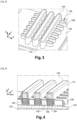
- at least one alternating stack 134 of portions 136 of the first material and portions 138 of the second material are shown on the Figure 1 , six distinct stacks 134 are shown, each comprising four portions 136 and three portions 138 stacked alternately on top of each other.
- Each of the stacks 134 has a substantially elongated shape, that is to say has a length (dimension along the X axis) greater than its width (dimension along the Y axis).
- the width of each stack 134 is for example between 20 nm and 200 nm, and the length of each stack 134 is for example greater than 100 nm.
- a thin dielectric layer 140 is then deposited conformally over the entire structure, that is to say by covering the upper faces and the lateral faces of the stacks 134 and the parts of the substrate 102 (of the buried dielectric layer 130 in the exemplary embodiment described) not covered by the stacks 134.
- the dielectric layer 140 comprises for example SiO 2 , which can be obtained from TEOS.
- At least one temporary gate 142 is then produced, covering a part of an upper face and lateral faces of the stacks 134.
- a material suitable for producing the temporary gates is deposited over the entire structure.
- the deposited material is polycrystalline silicon.
- the thickness of the deposited material is greater than the sum of the thicknesses of one of the stacks 134 and the dielectric layer 140, for example equal to 380 nm.
- a planarization, for example a CMP (chemical-mechanical planarization), of the deposited material is then implemented so that a given thickness, for example equal to 70 nm, is maintained above the stacks 134.
- a hard mask 144 is then produced on the material remaining after the planarization, the pattern of this hard mask defining that of the temporary gate(s) 142 to be produced.
- the hard mask 144 comprises a semiconductor nitride/semiconductor oxide bilayer such than SiN/SiO 2 .
- the remaining material suitable for producing the temporary grids is then etched in accordance with the pattern defined by the hard mask 144, forming the temporary grid(s) 142.
- several temporary grids 142 are produced (three temporary grids 142 are visible on the Figure 2 , each formed by covering the six stacks 134).
- each temporary grid 142 is for example between 10 nm and several hundred nm, and the length (dimension along the Y axis visible on the Figure 2 ) of each temporary grid 142 depends on the number of stacks 134 on which the temporary grids 142 must be produced, and for example equal to several tens of nm.
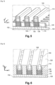
- Dielectric spacers 114 are then produced against the sides of the temporary gates 142.
- a layer of material suitable for producing these spacers 114 is deposited in a conformal manner over the entire structure, i.e. by covering the upper faces and the lateral faces of the stacks 134, the temporary gates 142 and the hard masks 144 and the parts of the substrate 102 (of the buried dielectric layer 130 in the embodiment described) not covered by the stacks 134 and the temporary gates 142.
- This material suitable for producing the dielectric spacers 114 corresponds for example to SiN, SiCO or SiBCN. The thickness of this layer is for example between 5 nm and 15 nm.
- An anisotropic etching of this layer is then implemented such that remaining portions of this layer arranged against the sides of the temporary gates 142 form the dielectric spacers 114 (see Figure 3 ). Remaining portions 146 of this layer arranged against the sides of the stacks 134 can be retained at the end of this etching, or can advantageously be removed.
- the anisotropic etching is implemented so as to remove the material located on the upper faces of the temporary gates 142 and the stacks 134. In addition, this etching also removes the parts of the layer 140 which are not covered by the temporary gates 142 and the dielectric spacers 114.
- the parts of the stacks 134 not covered by the temporary grids 142, by the dielectric spacers 114 or by the remaining portions 146 are etched. This etching is stopped on the buried dielectric layer 130.
- the remaining parts of the portions 136 are then etched partially and selectively with respect to the remaining parts of the portions 138, so as to form, directly above the dielectric spacers 114, spaces 148 above and below the ends of the remaining parts of the portions 138 (see Figure 4 ).
- the depth (dimension along the X axis on the Figure 4 ) etched in the remaining parts of the portions 136 is for example between 5 nm and 15 nm.
- the internal dielectric spacers 115 are then made in the spaces 148 previously formed. These internal dielectric spacers 115 are obtained by depositing a dielectric material, for example SiN, SiBCN or SiCO so as to at least fill the spaces 148. The material deposited outside the spaces 148 is etched isotropically in order to retain only the internal dielectric spacers 115 (see Figure 5 ).
- a dielectric material for example SiN, SiBCN or SiCO
- the insulating dielectric material 128 is deposited with a high thickness, then planarization is implemented until the hard mask 144 is reached.
- the hard mask 144 is then removed for example by wet etching, for example using a diluted H 3 PO 4 solution and used at a temperature of 110°C.
- the temporary gates 142 are then removed, for example by etching using a 0.5% diluted HF solution combined with a 1% diluted HCl solution and with a 5% TMAH solution. This etching is stopped when the remaining parts of the dielectric layer 140 are reached (see Figure 6 ).
- the remaining portions of the dielectric layer 140 are then etched, and then the remaining portions of the portions 136 are selectively etched with respect to the remaining portions of the portions 138, for example by implementing wet etching.
- the structure obtained at this stage is shown in the Figure 7 .
- At least one layer 112 intended to form the gate dielectrics of the selection transistors of the memory devices 100 is then deposited in a conforming manner, in particular in the spaces formed by the etching of the temporary gates 142 by covering the walls formed by the dielectric spacers 114 and the remaining parts of the portions 138.
- this layer comprises for example a material high-K dielectric (high dielectric permittivity) such as HfO 2 .
- this layer 112 intended to form the gate dielectrics may comprise SiO 2 or Al 2 O 3 or any other suitable material or combination of materials.
- Electrostatic control gates 110 of the selection transistors of the memory devices 100 are produced by depositing one or more conductive materials on the layer 112 intended to form the gate dielectrics of the selection transistors, by a first deposit of a thin layer of TiN (thickness for example equal to 3 nm) on which is stacked a layer of tungsten with a thickness for example equal to 200 nm.
- each of the gates 110 comprises an upper portion 106 and other portions 108 surrounding the remaining portions of the portions 138.
- the gates 110 comprise one or more materials different from TiN and W, such as for example doped polysilicon or any other metal (Mo, etc.).
- Planarization with stopping on the insulating dielectric material 128 is implemented to remove the material(s) of the layer 112 intended to form the gate dielectrics and the electrostatic control gates 110 deposited outside the spaces formed by the etching of the temporary gates 142.
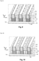
- cavities 150 comprising sidewalls formed by the dielectric spacers 114, the internal dielectric spacers 115 and, in the example described herein, remaining portions of the insulating dielectric material 128 (see Figure 9 ). These cavities 150 form locations for producing the contact regions of the devices 100.
- the portions 138 are then etched, for example by implementing chemical etching using a Hf-H 2 O 2 solution (see figures 10 And 11 ) when portions 138 contain SiGe. As can be seen on the Figure 11 representing a sectional view along the XX' axis shown on the Figure 10 , this etching forms tunnel-shaped spaces in which the transistor channels are intended to be made.
- a layer of semiconductor 120 is then deposited over the entire structure made at this stage of the process (see figures 12 And 13 ). First zones 122 of this semiconductor layer 120 which are located in the tunnel-shaped spaces previously formed are intended to form the channels of the selection transistors and are arranged against the gate dielectrics.
- Second zones 124 of this semiconductor layer 120 which cover the walls (side walls and bottom walls in the example described here) of the cavities 150 are intended to be in contact with the contact regions which will then be produced.
- the deposition is carried out without discontinuity, or without interruption, between the first and second zones 122 and 124.
- the semiconductor layer 120 comprises at least one 2D semiconductor material, for example a transition metal dichalcogenide such as MoS 2 , or WSe 2 , or WS 2 , or MoTe 2 . It is also possible that the material of the semiconductor layer 120 corresponds to IGZO, In 2 O 3 , IWO, ITO, or an amorphous semiconductor oxide, or any other suitable semiconductor material.
- a transition metal dichalcogenide such as MoS 2 , or WSe 2 , or WS 2 , or MoTe 2 .
- the material of the semiconductor layer 120 corresponds to IGZO, In 2 O 3 , IWO, ITO, or an amorphous semiconductor oxide, or any other suitable semiconductor material.
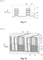
- One or more dielectric layers comprising for example Al 2 O 3 (or HfO 2 ) and/or SiO 2 (or a low-k dielectric, or with low dielectric permittivity), are then deposited and then etched isotropically in order to retain only portions 126 located in the tunnel-shaped spaces (see figures 14 And 15 ). These portions 126 form dielectric bars each surrounded by one of the first zones 122 of the semiconductor layer 120.
- the semiconductor layer 120 comprises several first zones 122 superimposed on top of each other by means of a succession of bars 126 and parts 108 of the gate 110 and gate dielectrics.
- contact regions 116, 118 are produced by depositing, in the example described, one or more metallic materials in the cavities 150 (see figure 16 ). Before this or these metal deposits, it is possible to deposit a layer of graphene in the cavities 150, this or these metals then being deposited on the layer of graphene.
- the contact regions 116, 118 comprise at least one metallic material such as gold, palladium, TiN, W, Ni, etc.
- each of the contact regions 116, 118 comprises a layer of TiN on which a portion of tungsten is formed.
- contact regions 116, 118 can be used to promote low resistances of contact, such as for example: S, Bi, Sn, Pd, Ru, Cu, Ni, Ti, TiN, W, Au, etc. These materials can also be modified subsequently (to improve their properties), by a doping step for example.
- These contact regions 116, 118 form the source / drain regions of the selection transistors of the memory devices 100.
- the contact region 118 comprises a memory stack 158, that is to say a stack of materials in which it is possible to carry out information storage.
- This memory stack 158 may correspond to a stack of materials of the FeRAM type including in this case a layer of ferroelectric material, or OxRAM including in this case an oxide layer, or CBRAM including in this case an ionic layer, for example a stack of the MIM (metal - insulator - metal) type.
- MIM metal - insulator - metal
- This memory stack 158 is arranged within the metallic material(s) forming the remainder of the contact region 118. A portion of the metallic material(s) is interposed between the memory stack 158 and the portions of the semiconductor layer 120 located in the cavity 150 in which the contact region 118 is made. Thus, the memory stack 158 is interposed between a first conductive portion 157 of the contact region 118, electrically connecting the memory stack 158 to the semiconductor layer 120, and a second conductive portion 156 of the contact region 118 forming an electrical contact of the memory stack 158.
- These contact regions 116 and 118 are electrically coupled to the first zones 122 of the semiconductor layer 120 via the second zones 124 of the semiconductor layer 120 which extend between the contact regions 116, 118 and the dielectric spacers 114 as well as against the other walls of the contact regions 116, 118 located in the cavities 150.
- the material of these regions deposited outside the cavities 150 is removed by implementing planarization with a stop on the dielectric insulation material 128.
- the devices obtained at the end of this process correspond to the devices 100 represented on the figure 16 .
- the semiconductor layer 120 does not completely fill the spaces formed by the etching of the portions 138, and of the dielectric portions 126 are made in the spaces remaining after the deposition of the semiconductor layer 120.
- the dielectric portions 126 it is possible not to produce the dielectric portions 126, the semiconductor layer 120 filling in this case, during its deposition, the remaining spaces formed by the etching of the portions 138.
- the layer 112 forming the gate dielectric of the selection transistor of the memory device 100 is not deposited just before the production of the gate 110 as previously described, but that this layer is deposited in the spaces formed by the etching of the portions 138 and in the cavities 1150, just before the deposition of the semiconductor layer 120.
- the layer 112 covers the different walls on which the material of the semiconductor layer 120 is intended to be deposited, thus homogenizing the surfaces, and therefore the interfaces, against which the semiconductor layer 120 is then deposited.
- the layer 112 it is possible for the layer 112 to be deposited during two different stages: firstly just before the production of the grid 110 as previously described in connection with the figure 8 , then in the spaces formed by the etching of the portions 138 and in the cavities 150, just before the deposition of the semiconductor layer 120.
- the parts of the layer 112 located directly above the gate 110 are thicker than the other parts of the layer 112 because these parts combine the thicknesses of material deposited during the two deposition steps.
- all the side walls of the cavities 150 are covered by the second zones 124 of the semiconductor layer 120.
- the layer 112 forming the gate dielectrics is deposited over the entire structure (see Figure 17 ). Portions of this layer 112 are located in the previously formed tunnel-like spaces, thus forming the gate dielectrics, and other portions of this layer 112 cover the walls of the cavities 150.
- the semiconductor layer 120 is then deposited over the entire structure, covering the layer 112 forming the gate dielectrics (see figure 18 ), so as to completely fill the remaining tunnel-shaped spaces.
- the cavities 150 are not completely filled by the deposition of the semiconductor layer 120 and the layer 112 forming the gate dielectrics.
- the contact regions 116, 118 are then produced, for example by making a first deposit (for example ALD) of TiN (designated by the reference 154 on the figure 19 ), then filling the rest of the available space with tungsten (designated by the reference 156 on the figure 20 ). In the example described here, this deposition of tungsten also completes the production of the control gate 110. In addition, during the deposition of tungsten, it is stopped to produce the memory stack 158 within the contact region 118, then resumed to complete the production of the contact regions 116, 118.
- ALD first deposit
- tungsten designated by the reference 154 on the figure 19
- One of the above variants can be implemented without the other being implemented.
- the dielectric portions 126 can be produced as previously described in connection with the figures 14 And 15 .
- control grid 110 is common to several devices 100, that is to say simultaneously controls these different devices, the contact regions 116, 118 of which are electrically isolated from those of the other neighboring devices 100 by the portions of the dielectric insulating material 128.
- the grids 110 produced are not common to the different devices 100 produced.
- each of the first zones 122 of the semiconductor layer 120 may be surrounded by the same electrostatic control grid 110, as is the case in the examples previously described, or by an electrostatic control grid different from that surrounding the other first zones 122 of the semiconductor layer 120.
- each of the contact regions 116, 118 is arranged in a cavity comprising side walls formed by the dielectric spacers 114, 115 and by a dielectric insulating material 128.
- the second zones 124 of the semiconductor layer 120 cover the side walls and the bottom walls of the cavities in which the contact regions 116, 118 are arranged.
- contact regions it is possible for contact regions to be common to several devices 100.
- the dielectric insulation material 128 is not present so that the same contact region, for example the contact region 118 including the memory stack 158, is electrically coupled to the channels of these two neighboring devices 100.
- Such a configuration allows for example the production of memory devices of the 2T1R or 2T1C type.
Landscapes
- Semiconductor Memories (AREA)
- Non-Volatile Memory (AREA)
- Thin Film Transistor (AREA)
Claims (14)
- Speichervorrichtung (100) umfassend mindestens einen Speicherstapel (158), der elektrisch in Reihe mit einem Auswahltransistor verbunden ist, wobei die Speichervorrichtung (100) ein Substrat (102) umfasst, an dem der Auswahltransistor Folgendes umfasst:- eine Halbleiterschicht (120), umfassend mehrere erste Bereiche (122), die übereinander angeordnet sind, wobei die ersten Bereiche (122) einen elektrisch leitenden Kanal des Auswahltransistors bilden;- ein elektrostatisches Steuergitter (110) und eine Gitterdielektrizitätsschicht (112) des Auswahltransistors, wobei die Teile der Gitterdielektrizitätsschicht (112) jeweils zwischen einem Teil (106, 108) des elektrostatischen Steuergitters (110) und einem der ersten Bereiche (122) der Halbleiterschicht (120) angeordnet sind;- dielektrische Abstandshalter (114), die an Flanken des elektrostatischen Steuergitters (110) angeordnet sind;- Kontaktbereiche (116, 118), die über zweite Bereiche (124) der Halbleiterschicht (120) elektrisch mit den ersten Bereichen (122) der Halbleiterschicht (120) gekoppelt sind, wobei sich die zweiten Bereiche (124) der Halbleiterschicht (120) zwischen den Kontaktbereichen (116, 118) und den dielektrischen Abstandshaltern (114) erstrecken, wobei die Kontaktbereiche (116, 118) Source-/Drain-Bereiche des Auswahltransistors bilden,wobei einer der Kontaktbereiche (118) den Speicherstapel (158) umfasst, der zwischen einem ersten leitenden Abschnitt (157) eingelegt ist, der den Speicherstapel (158) mit der Halbleiterschicht (120) elektrisch verbindet, und einem zweiten leitenden Abschnitt (156), der einen elektrischen Kontakt des Speicherstapels (158) bildet; und wobei die zweiten Bereiche (124) der Halbleiterschicht (120) nicht direkt gegen das elektrostatische Steuergitter (110) angeordnet sind und zusammen mit den ersten Bereichen (122) eine durchgehende Schicht bilden.
- Speichervorrichtung (100) nach Anspruch 1, wobei die Halbleiterschicht (120) ein zweidimensionales oder ein anderes durch MOCVD, CVD oder ALD hinterlegtes Halbleitermaterial aufweist.
- Speichervorrichtung (100) nach einem der vorstehenden Ansprüche, wobei:- jeder der Kontaktbereiche (116, 118) in einem Hohlraum (150) angeordnet ist, der Seitenwände umfasst, die mindestens durch die dielektrischen Abstandshalter (114) und durch ein dielektrisches Isolationsmaterial (128) gebildet sind;- die zweiten Bereiche (124) der Halbleiterschicht (120) mindestens einen Teil der Wände der Hohlräume (150) bedecken, in denen die Kontaktbereiche (116, 118) angeordnet sind.
- Speichervorrichtung (100) nach einem der vorstehenden Ansprüche, wobei jeder der ersten Bereiche (122) der Halbleiterschicht (120) von demselben elektrostatischen Steuergitter (110) oder von einem elektrostatischen Steuergitter (110) umgeben ist, das sich von dem unterscheidet, welches die anderen ersten Bereiche (122) der Halbleiterschicht (120) umgibt.
- Speichervorrichtung (100) nach einem der vorstehenden Ansprüche, die weiter einen oder mehrere dielektrische Abschnitte (126) aufweist, die jeweils zwischen zwei ersten Bereichen (122) der Halbleiterschicht (120) und derart angeordnet sind, dass jeder der dielektrischen Abschnitte (126) von einem der ersten Bereiche (122) der Halbleiterschicht (120) umgeben ist.
- Speichervorrichtung (100) nach einem der vorstehenden Ansprüche, die weiter innere dielektrische Abstandshalter (115) aufweist, die an Flanken eines oder mehrerer Teile (108) des elektrostatischen Steuergitters (110) angeordnet sind.
- Speichervorrichtung (100) nach einem der vorhergehenden Ansprüche, wobei der Speicherstapel (158) eine Schicht aus ferroelektrischem Material oder eine Oxid- oder lonenschicht aufweist.
- Mikroelektronische Komponente (1000), aufweisend mehrere mikroelektronische Vorrichtungen (100) nach einem der vorstehenden Ansprüche, und wobei:- die elektrostatischen Steuergitter (110) der Auswahltransistoren mehrerer Speichervorrichtungen (100) gemein sind und einstückig von denselben Materialabschnitten gebildet werden, und/oder- einer der Kontaktbereiche (116, 118) zwei benachbarten Auswahltransistoren von Speichervorrichtungen (100) gemein ist.
- Verfahren zum Herstellen einer Speichervorrichtung (100) umfassend mindestens einen Speicherstapel (158), der elektrisch in Reihe mit einem Auswahltransistor verbunden ist, umfassend:a) Herstellen, auf einem Substrat (102), mindestens eines abwechselnden Stapels (134) aus Abschnitten eines ersten Materials (136) und Abschnitten eines zweiten Materials (138), wobei das erste und das zweite Material selektiv in Bezug zueinander geätzt werden können, anschließendb) Herstellen eines temporären Gitters (142), das einen Teil einer oberen Fläche und von Seitenflächen des Stapels (134) bedeckt, anschließendc) Herstellen von dielektrischen Abstandshaltern (114) an Flanken des temporären Gitters (142), anschließendd) Ätzen von Teilen des Stapels (134), die nicht von dem temporären Gitter (142) und den dielektrischen Abstandshaltern (114) bedeckt sind, anschließende) Ätzen des temporären Gitters (142), anschließendf) selektives Ätzen der Abschnitte des ersten Materials (136) in Bezug auf die Abschnitte des zweiten Materials (138), anschließendg) Herstellen mindestens eines Teils eines elektrostatischen Steuergitters (110) in einem Raum, der durch das Ätzen des temporären Gitters (142) gebildet wurde, derart, dass die dielektrischen Abstandshalter (114) an den Flanken des elektrostatischen Steuergitter (110) angeordnet sind, anschließendh) Ätzen der Abschnitte des zweiten Materials (138), anschließendi) Herstellen einer Halbleiterschicht (120) mit mehreren ersten Bereichen (122), die so eingerichtet sind, dass sie einen elektrisch leitenden Kanal des Auswahltransistors bilden, und die gegen das Gitter (110) an Stellen angeordnet sind, die durch das Ätzen von Abschnitten des zweiten Materials (138) gebildet werden, wobei sich die Halbleiterschicht (120) ohne Unterbrechung zu den ersten Bereichen (122) fortsetzt, indem sie zweite Bereiche (124) bildet, die zumindest einen Teil der Flanken der dielektrischen Abstandshalter (114) bedecken und die nicht direkt gegen das elektrostatische Steuergitter (110) angeordnet sind, und anschließendj) Herstellen, auf dem Substrat (102), von Kontaktbereichen (116, 118), die elektrisch mit den ersten Bereichen (122) der Halbleiterschicht (120) durch die zweiten Bereiche (124) der Halbleiterschicht (120) gekoppelt sind, wobei jeder zweite Bereich (124) der Halbleiterschicht (120) sich zwischen den Kontaktbereichen (116, 118) und den dielektrischen Abstandshaltern (114) erstreckt, wobei die Kontaktbereiche (116, 118) Source-/Drain-Bereiche des Auswahltransistors bilden, wobei einer der Kontaktbereiche (118) den Speicherstapel (158) aufweist, der zwischen einen ersten leitenden Abschnitt (157) eingelegt ist, der den Speicherstapel (158) mit der Halbleiterschicht (120) elektrisch verbindet, und einen zweiten leitenden Abschnitt (156), der einen elektrischen Kontakt des Speicherstapels (158) bildet, wobei das Verfahren ferner das Herstellen einer Gitterdielektrizitätsschicht des Auswahltransistors aufweist, so dass Teile der Gitterdielektrizitätsschicht jeweils zwischen einem Teil des elektrostatischen Steuergitters und einem der ersten Bereiche der Halbleiterschicht angeordnet sind.
- Verfahren nach Anspruch 9, umfassend unter anderem, zwischen den Schritten d) und e), ein Abscheiden eines dielektrischen Isolationsmaterials (128) um die dielektrischen Abstandshalter (114) herum, und anschließend ein Ätzen von Hohlräumen (150) in dem dielektrischen Isolationsmaterial (128) derart, dass jeder der Hohlräume (150) mindestens eine Seitenwand umfasst, die von einem der dielektrischen Abstandshalter (114) gebildet wird, und wobei:- Schritt i) so ausgeführt ist, dass die zweiten Bereiche (124) der Halbleiterschicht (120) mindestens einen Teil der Seitenwände der Hohlräume (150) bedecken, und- Schritt j) so ausgeführt ist, dass jeder der Kontaktbereiche (116, 118) in einem der Hohlräume (150) angeordnet ist.
- Verfahren nach einem der Ansprüche 9 oder 10, umfassend einen Schritt der Ablagerung der Gitterdielektrizitätsschicht (112) des ausgeführten Auswahltransistors:- zwischen den Schritten f) und g), in dem durch die Gravur des temporären Gitters (142) gebildeten Raum, wobei das elektrostatische Steuergitter (110) des Auswahltransistors in diesem Fall auf der Gitterdielektrizitätsschicht (112) ausgeführt ist, und/oder- zwischen den Schritten h) und i), in den durch das Ätzen der Abschnitte des zweiten Materials (138) gebildeten Stellen, wobei die Halbleiterschicht (120) anschließend hergestellt wird, indem die Gitterdielektrizitätsschicht (112) bedeckt wird.
- Verfahren nach einem der Ansprüche 9 bis 11, wobei Schritt i) derart ausgeführt wird, dass die ersten Bereiche (122) der Halbleiterschicht (120) Wände der Stellen, die durch das Ätzen der Abschnitte des zweiten Materials (138) gebildet wurden, bedecken, und das Verfahren zwischen den Schritten i) und j) weiter ein Herstellen von dielektrischen Abschnitten (126) in verbleibenden Räumen der Stellen und derart umfasst, dass jeder der dielektrischen Abschnitte (126) von den ersten Bereichen (122) der Halbleiterschicht (120) umgeben ist.
- Verfahren nach einem der Ansprüche 9 bis 11, wobei Schritt i) derart ausgeführt wird, dass die ersten Bereiche (122) der Halbleiterschicht (120) die Stellen, die durch das Ätzen der Abschnitte des zweiten Materials (138) gebildet wurden, vollständig füllen.
- Verfahren nach einem der Ansprüche 9 bis 13, umfassend zwischen den Schritten d) und e) weiter ein Ätzen von Teilen der Abschnitte des ersten Materials (136), die senkrecht zu den dielektrischen Abstandshaltern (114) angeordnet sind, und ein Herstellen von inneren dielektrischen Abstandshaltern (115) anstelle der geätzten Teile der Abschnitte des ersten Materials (136).
Applications Claiming Priority (1)
| Application Number | Priority Date | Filing Date | Title |
|---|---|---|---|
| FR2214257A FR3144405B1 (fr) | 2022-12-22 | 2022-12-22 | Dispositif memoire comprenant d’importantes surfaces de contact entre le canal de conduction et les regions de contact |
Publications (2)
| Publication Number | Publication Date |
|---|---|
| EP4391069A1 EP4391069A1 (de) | 2024-06-26 |
| EP4391069B1 true EP4391069B1 (de) | 2025-06-11 |
Family
ID=86942492
Family Applications (1)
| Application Number | Title | Priority Date | Filing Date |
|---|---|---|---|
| EP23218847.4A Active EP4391069B1 (de) | 2022-12-22 | 2023-12-20 | Speicheranordnung mit grossen kontaktflächen zwischen leitungskanal und kontaktbereichen |
Country Status (6)
| Country | Link |
|---|---|
| US (1) | US20240215263A1 (de) |
| EP (1) | EP4391069B1 (de) |
| JP (1) | JP2024091575A (de) |
| CN (1) | CN118251015A (de) |
| FR (1) | FR3144405B1 (de) |
| TW (1) | TW202441598A (de) |
Family Cites Families (5)
| Publication number | Priority date | Publication date | Assignee | Title |
|---|---|---|---|---|
| US9892972B2 (en) * | 2009-10-12 | 2018-02-13 | Monolithic 3D Inc. | 3D semiconductor device and structure |
| US12176388B2 (en) * | 2020-06-26 | 2024-12-24 | Intel Corporation | Transition metal dichalcogenide nanowires and methods of fabrication |
| US11728391B2 (en) | 2020-08-07 | 2023-08-15 | Taiwan Semiconductor Manufacturing Co., Ltd. | 2d-channel transistor structure with source-drain engineering |
| US12266712B2 (en) * | 2020-12-23 | 2025-04-01 | Intel Corporation | Transition metal dichalcogenide nanosheet transistors and methods of fabrication |
| FR3123150B1 (fr) * | 2021-05-20 | 2023-05-26 | Commissariat Energie Atomique | Memoire 1t1r a structure 3d |
-
2022
- 2022-12-22 FR FR2214257A patent/FR3144405B1/fr active Active
-
2023
- 2023-12-19 TW TW112149562A patent/TW202441598A/zh unknown
- 2023-12-20 EP EP23218847.4A patent/EP4391069B1/de active Active
- 2023-12-21 US US18/393,200 patent/US20240215263A1/en active Pending
- 2023-12-21 JP JP2023215864A patent/JP2024091575A/ja active Pending
- 2023-12-22 CN CN202311790252.4A patent/CN118251015A/zh active Pending
Also Published As
| Publication number | Publication date |
|---|---|
| TW202441598A (zh) | 2024-10-16 |
| JP2024091575A (ja) | 2024-07-04 |
| FR3144405B1 (fr) | 2024-12-20 |
| FR3144405A1 (fr) | 2024-06-28 |
| CN118251015A (zh) | 2024-06-25 |
| EP4391069A1 (de) | 2024-06-26 |
| US20240215263A1 (en) | 2024-06-27 |
Similar Documents
| Publication | Publication Date | Title |
|---|---|---|
| FR3086456A1 (fr) | Procede de realisation de transistors superposes | |
| CN113889480A (zh) | 三维存储器器件及其制造方法 | |
| FR3060839A1 (fr) | Procede de realisation d'un dispositif semi-conducteur a nanofil et espaceurs externe et interne alignes | |
| EP4092750B1 (de) | 1t1r-speicher mit 3d-struktur | |
| FR3016237A1 (fr) | Dispositif a nanofils de semi-conducteur partiellement entoures par une grille | |
| FR2979481A1 (fr) | Procede de realisation d'un circuit integre tridimensionnel | |
| WO2007110507A2 (fr) | Procede de realisation d'un transistor a effet de champ a grilles auto-alignees | |
| WO2008155379A2 (fr) | Transistor a effet de champ a contacts electriques alternes | |
| EP4391081B1 (de) | Mikroelektronische vorrichtung mit kontaktflächen zwischen leitungskanal und source- und drain-bereichen | |
| FR2818439A1 (fr) | Procede de fabrication d'un ilot de matiere confine entre des electrodes, et applications aux transistors | |
| EP4391069B1 (de) | Speicheranordnung mit grossen kontaktflächen zwischen leitungskanal und kontaktbereichen | |
| EP4639635A1 (de) | Mikroelektronische fet-vorrichtung mit grossen kontaktflächen zwischen dem leitungskanal und den source- und drain-regionen | |
| EP3079178B1 (de) | Herstellungsverfahren eines integrierten schaltkreises, in den ein fet-transistor und ein oxram-speicherpunkt integriert sind | |
| FR3144408A1 (fr) | Dispositif microelectronique comprenant d’importantes surfaces de contact entre le canal de conduction et les regions de source et drain | |
| EP3046143A1 (de) | Verfahren zur herstellung eines dreidimensionalen integrierten schaltkreises | |
| EP4391078A2 (de) | Fet-mikroelektronische vorrichtung mit grossen kontaktflächen zwischen leitungskanal und source- und drain-bereichen | |
| FR3143797A1 (fr) | Electrodes d'échange pour réseau d’ilots quantiques | |
| EP4507005B1 (de) | Verfahren zur herstellung einer vorrichtung mit übereinanderliegenden transistoren | |
| EP4507004B1 (de) | Mikroelektronische vorrichtung mit einem mantelgitter und verfahren zur herstellung einer solchen vorrichtung | |
| JP7838907B2 (ja) | 二次元チャネルを有する半導体構造 | |
| CN118248728A (zh) | 导电通道与源极漏极区域间包括大接触表面的微电子器件 | |
| FR3166241A1 (fr) | Dispositif microélectronique comprenant une grille enrobante et procédé de réalisation | |
| EP4507006A1 (de) | Verfahren zur herstellung einer mikroelektronischen vorrichtung mit einem integrierten gate | |
| FR3125915A1 (fr) | Procede de gravure selective isotrope de silicium | |
| EP4507008A1 (de) | Mikroelektronische vorrichtung mit einem mantelgitter und verfahren zur herstellung einer solchen vorrichtung |
Legal Events
| Date | Code | Title | Description |
|---|---|---|---|
| PUAI | Public reference made under article 153(3) epc to a published international application that has entered the european phase |
Free format text: ORIGINAL CODE: 0009012 |
|
| STAA | Information on the status of an ep patent application or granted ep patent |
Free format text: STATUS: REQUEST FOR EXAMINATION WAS MADE |
|
| 17P | Request for examination filed |
Effective date: 20231220 |
|
| AK | Designated contracting states |
Kind code of ref document: A1 Designated state(s): AL AT BE BG CH CY CZ DE DK EE ES FI FR GB GR HR HU IE IS IT LI LT LU LV MC ME MK MT NL NO PL PT RO RS SE SI SK SM TR |
|
| RAP3 | Party data changed (applicant data changed or rights of an application transferred) |
Owner name: COMMISSARIAT A L'ENERGIE ATOMIQUE ET AUX ENERGIESALTERNATIVES |
|
| REG | Reference to a national code |
Ref country code: DE Ref legal event code: R079 Free format text: PREVIOUS MAIN CLASS: H01L0029060000 Ipc: H10B0063000000 Ref country code: DE Ref legal event code: R079 Ref document number: 602023003972 Country of ref document: DE Free format text: PREVIOUS MAIN CLASS: H01L0029060000 Ipc: H10B0063000000 |
|
| RIC1 | Information provided on ipc code assigned before grant |
Ipc: H10D 64/27 20250101ALN20250213BHEP Ipc: H10D 30/43 20250101ALN20250213BHEP Ipc: H10D 30/01 20250101ALN20250213BHEP Ipc: B82Y 10/00 20110101ALN20250213BHEP Ipc: H10B 53/30 20230101ALI20250213BHEP Ipc: H10B 53/20 20230101ALI20250213BHEP Ipc: H10B 51/20 20230101ALI20250213BHEP Ipc: H10D 99/00 20250101ALI20250213BHEP Ipc: H10D 64/62 20250101ALI20250213BHEP Ipc: H10D 64/01 20250101ALI20250213BHEP Ipc: H10D 62/80 20250101ALI20250213BHEP Ipc: H10D 62/13 20250101ALI20250213BHEP Ipc: H10D 62/10 20250101ALI20250213BHEP Ipc: H10D 30/69 20250101ALI20250213BHEP Ipc: H10D 30/67 20250101ALI20250213BHEP Ipc: H10D 30/47 20250101ALI20250213BHEP Ipc: H10B 63/00 20230101AFI20250213BHEP Ipc: H10B 51/30 20230101ALI20250213BHEP |
|
| GRAP | Despatch of communication of intention to grant a patent |
Free format text: ORIGINAL CODE: EPIDOSNIGR1 |
|
| STAA | Information on the status of an ep patent application or granted ep patent |
Free format text: STATUS: GRANT OF PATENT IS INTENDED |
|
| INTG | Intention to grant announced |
Effective date: 20250327 |
|
| RIN1 | Information on inventor provided before grant (corrected) |
Inventor name: REBOH, SHAY Inventor name: COQUAND, REMI Inventor name: BARRAUD, SYLVAIN |
|
| GRAS | Grant fee paid |
Free format text: ORIGINAL CODE: EPIDOSNIGR3 |
|
| GRAA | (expected) grant |
Free format text: ORIGINAL CODE: 0009210 |
|
| STAA | Information on the status of an ep patent application or granted ep patent |
Free format text: STATUS: THE PATENT HAS BEEN GRANTED |
|
| AK | Designated contracting states |
Kind code of ref document: B1 Designated state(s): AL AT BE BG CH CY CZ DE DK EE ES FI FR GB GR HR HU IE IS IT LI LT LU LV MC ME MK MT NL NO PL PT RO RS SE SI SK SM TR |
|
| REG | Reference to a national code |
Ref country code: GB Ref legal event code: FG4D Free format text: NOT ENGLISH |
|
| REG | Reference to a national code |
Ref country code: CH Ref legal event code: EP |
|
| REG | Reference to a national code |
Ref country code: DE Ref legal event code: R096 Ref document number: 602023003972 Country of ref document: DE |
|
| REG | Reference to a national code |
Ref country code: IE Ref legal event code: FG4D Free format text: LANGUAGE OF EP DOCUMENT: FRENCH |
|
| PG25 | Lapsed in a contracting state [announced via postgrant information from national office to epo] |
Ref country code: ES Free format text: LAPSE BECAUSE OF FAILURE TO SUBMIT A TRANSLATION OF THE DESCRIPTION OR TO PAY THE FEE WITHIN THE PRESCRIBED TIME-LIMIT Effective date: 20250611 Ref country code: FI Free format text: LAPSE BECAUSE OF FAILURE TO SUBMIT A TRANSLATION OF THE DESCRIPTION OR TO PAY THE FEE WITHIN THE PRESCRIBED TIME-LIMIT Effective date: 20250611 |
|
| REG | Reference to a national code |
Ref country code: LT Ref legal event code: MG9D |
|
| PG25 | Lapsed in a contracting state [announced via postgrant information from national office to epo] |
Ref country code: GR Free format text: LAPSE BECAUSE OF FAILURE TO SUBMIT A TRANSLATION OF THE DESCRIPTION OR TO PAY THE FEE WITHIN THE PRESCRIBED TIME-LIMIT Effective date: 20250912 Ref country code: NO Free format text: LAPSE BECAUSE OF FAILURE TO SUBMIT A TRANSLATION OF THE DESCRIPTION OR TO PAY THE FEE WITHIN THE PRESCRIBED TIME-LIMIT Effective date: 20250911 |
|
| REG | Reference to a national code |
Ref country code: NL Ref legal event code: MP Effective date: 20250611 |
|
| PG25 | Lapsed in a contracting state [announced via postgrant information from national office to epo] |
Ref country code: BG Free format text: LAPSE BECAUSE OF FAILURE TO SUBMIT A TRANSLATION OF THE DESCRIPTION OR TO PAY THE FEE WITHIN THE PRESCRIBED TIME-LIMIT Effective date: 20250611 |
|
| PG25 | Lapsed in a contracting state [announced via postgrant information from national office to epo] |
Ref country code: HR Free format text: LAPSE BECAUSE OF FAILURE TO SUBMIT A TRANSLATION OF THE DESCRIPTION OR TO PAY THE FEE WITHIN THE PRESCRIBED TIME-LIMIT Effective date: 20250611 |
|
| PG25 | Lapsed in a contracting state [announced via postgrant information from national office to epo] |
Ref country code: RS Free format text: LAPSE BECAUSE OF FAILURE TO SUBMIT A TRANSLATION OF THE DESCRIPTION OR TO PAY THE FEE WITHIN THE PRESCRIBED TIME-LIMIT Effective date: 20250911 |
|
| PG25 | Lapsed in a contracting state [announced via postgrant information from national office to epo] |
Ref country code: LV Free format text: LAPSE BECAUSE OF FAILURE TO SUBMIT A TRANSLATION OF THE DESCRIPTION OR TO PAY THE FEE WITHIN THE PRESCRIBED TIME-LIMIT Effective date: 20250611 |
|
| PG25 | Lapsed in a contracting state [announced via postgrant information from national office to epo] |
Ref country code: NL Free format text: LAPSE BECAUSE OF FAILURE TO SUBMIT A TRANSLATION OF THE DESCRIPTION OR TO PAY THE FEE WITHIN THE PRESCRIBED TIME-LIMIT Effective date: 20250611 |
|
| PG25 | Lapsed in a contracting state [announced via postgrant information from national office to epo] |
Ref country code: PT Free format text: LAPSE BECAUSE OF FAILURE TO SUBMIT A TRANSLATION OF THE DESCRIPTION OR TO PAY THE FEE WITHIN THE PRESCRIBED TIME-LIMIT Effective date: 20251013 |
|
| REG | Reference to a national code |
Ref country code: AT Ref legal event code: MK05 Ref document number: 1803293 Country of ref document: AT Kind code of ref document: T Effective date: 20250611 |
|
| PG25 | Lapsed in a contracting state [announced via postgrant information from national office to epo] |
Ref country code: IS Free format text: LAPSE BECAUSE OF FAILURE TO SUBMIT A TRANSLATION OF THE DESCRIPTION OR TO PAY THE FEE WITHIN THE PRESCRIBED TIME-LIMIT Effective date: 20251011 |
|
| PG25 | Lapsed in a contracting state [announced via postgrant information from national office to epo] |
Ref country code: AT Free format text: LAPSE BECAUSE OF FAILURE TO SUBMIT A TRANSLATION OF THE DESCRIPTION OR TO PAY THE FEE WITHIN THE PRESCRIBED TIME-LIMIT Effective date: 20250611 Ref country code: SM Free format text: LAPSE BECAUSE OF FAILURE TO SUBMIT A TRANSLATION OF THE DESCRIPTION OR TO PAY THE FEE WITHIN THE PRESCRIBED TIME-LIMIT Effective date: 20250611 |
|
| PGFP | Annual fee paid to national office [announced via postgrant information from national office to epo] |
Ref country code: FR Payment date: 20251222 Year of fee payment: 3 |
|
| PG25 | Lapsed in a contracting state [announced via postgrant information from national office to epo] |
Ref country code: CZ Free format text: LAPSE BECAUSE OF FAILURE TO SUBMIT A TRANSLATION OF THE DESCRIPTION OR TO PAY THE FEE WITHIN THE PRESCRIBED TIME-LIMIT Effective date: 20250611 |
|
| PG25 | Lapsed in a contracting state [announced via postgrant information from national office to epo] |
Ref country code: PL Free format text: LAPSE BECAUSE OF FAILURE TO SUBMIT A TRANSLATION OF THE DESCRIPTION OR TO PAY THE FEE WITHIN THE PRESCRIBED TIME-LIMIT Effective date: 20250611 |
|
| PG25 | Lapsed in a contracting state [announced via postgrant information from national office to epo] |
Ref country code: EE Free format text: LAPSE BECAUSE OF FAILURE TO SUBMIT A TRANSLATION OF THE DESCRIPTION OR TO PAY THE FEE WITHIN THE PRESCRIBED TIME-LIMIT Effective date: 20250611 |
|
| PG25 | Lapsed in a contracting state [announced via postgrant information from national office to epo] |
Ref country code: SK Free format text: LAPSE BECAUSE OF FAILURE TO SUBMIT A TRANSLATION OF THE DESCRIPTION OR TO PAY THE FEE WITHIN THE PRESCRIBED TIME-LIMIT Effective date: 20250611 |
|
| PG25 | Lapsed in a contracting state [announced via postgrant information from national office to epo] |
Ref country code: RO Free format text: LAPSE BECAUSE OF FAILURE TO SUBMIT A TRANSLATION OF THE DESCRIPTION OR TO PAY THE FEE WITHIN THE PRESCRIBED TIME-LIMIT Effective date: 20250611 |
|
| REG | Reference to a national code |
Ref country code: DE Ref legal event code: R097 Ref document number: 602023003972 Country of ref document: DE |
|
| PG25 | Lapsed in a contracting state [announced via postgrant information from national office to epo] |
Ref country code: DK Free format text: LAPSE BECAUSE OF FAILURE TO SUBMIT A TRANSLATION OF THE DESCRIPTION OR TO PAY THE FEE WITHIN THE PRESCRIBED TIME-LIMIT Effective date: 20250611 |
|
| PGFP | Annual fee paid to national office [announced via postgrant information from national office to epo] |
Ref country code: DE Payment date: 20251222 Year of fee payment: 3 |
|
| PG25 | Lapsed in a contracting state [announced via postgrant information from national office to epo] |
Ref country code: IT Free format text: LAPSE BECAUSE OF FAILURE TO SUBMIT A TRANSLATION OF THE DESCRIPTION OR TO PAY THE FEE WITHIN THE PRESCRIBED TIME-LIMIT Effective date: 20250611 |
|
| PLBE | No opposition filed within time limit |
Free format text: ORIGINAL CODE: 0009261 |
|
| STAA | Information on the status of an ep patent application or granted ep patent |
Free format text: STATUS: NO OPPOSITION FILED WITHIN TIME LIMIT |
|
| REG | Reference to a national code |
Ref country code: CH Ref legal event code: L10 Free format text: ST27 STATUS EVENT CODE: U-0-0-L10-L00 (AS PROVIDED BY THE NATIONAL OFFICE) Effective date: 20260423 |