EP4386815A2 - Verfahren zur herstellung eines sige-kanal-feldeffekttransistors - Google Patents
Verfahren zur herstellung eines sige-kanal-feldeffekttransistors Download PDFInfo
- Publication number
- EP4386815A2 EP4386815A2 EP23215728.9A EP23215728A EP4386815A2 EP 4386815 A2 EP4386815 A2 EP 4386815A2 EP 23215728 A EP23215728 A EP 23215728A EP 4386815 A2 EP4386815 A2 EP 4386815A2
- Authority
- EP
- European Patent Office
- Prior art keywords
- layer
- gate oxide
- oxide layer
- germanium
- silicon
- Prior art date
- Legal status (The legal status is an assumption and is not a legal conclusion. Google has not performed a legal analysis and makes no representation as to the accuracy of the status listed.)
- Granted
Links
Images


Classifications
-
- H—ELECTRICITY
- H10—SEMICONDUCTOR DEVICES; ELECTRIC SOLID-STATE DEVICES NOT OTHERWISE PROVIDED FOR
- H10P—GENERIC PROCESSES OR APPARATUS FOR THE MANUFACTURE OR TREATMENT OF DEVICES COVERED BY CLASS H10
- H10P34/00—Irradiation with electromagnetic or particle radiation of wafers, substrates or parts of devices
- H10P34/40—Irradiation with electromagnetic or particle radiation of wafers, substrates or parts of devices with high-energy radiation
- H10P34/42—Irradiation with electromagnetic or particle radiation of wafers, substrates or parts of devices with high-energy radiation with electromagnetic radiation, e.g. laser annealing
-
- H—ELECTRICITY
- H10—SEMICONDUCTOR DEVICES; ELECTRIC SOLID-STATE DEVICES NOT OTHERWISE PROVIDED FOR
- H10D—INORGANIC ELECTRIC SEMICONDUCTOR DEVICES
- H10D30/00—Field-effect transistors [FET]
- H10D30/01—Manufacture or treatment
- H10D30/021—Manufacture or treatment of FETs having insulated gates [IGFET]
-
- H—ELECTRICITY
- H10—SEMICONDUCTOR DEVICES; ELECTRIC SOLID-STATE DEVICES NOT OTHERWISE PROVIDED FOR
- H10D—INORGANIC ELECTRIC SEMICONDUCTOR DEVICES
- H10D30/00—Field-effect transistors [FET]
- H10D30/01—Manufacture or treatment
- H10D30/021—Manufacture or treatment of FETs having insulated gates [IGFET]
- H10D30/027—Manufacture or treatment of FETs having insulated gates [IGFET] of lateral single-gate IGFETs
-
- H—ELECTRICITY
- H10—SEMICONDUCTOR DEVICES; ELECTRIC SOLID-STATE DEVICES NOT OTHERWISE PROVIDED FOR
- H10D—INORGANIC ELECTRIC SEMICONDUCTOR DEVICES
- H10D30/00—Field-effect transistors [FET]
- H10D30/60—Insulated-gate field-effect transistors [IGFET]
- H10D30/751—Insulated-gate field-effect transistors [IGFET] having composition variations in the channel regions
-
- H—ELECTRICITY
- H10—SEMICONDUCTOR DEVICES; ELECTRIC SOLID-STATE DEVICES NOT OTHERWISE PROVIDED FOR
- H10D—INORGANIC ELECTRIC SEMICONDUCTOR DEVICES
- H10D62/00—Semiconductor bodies, or regions thereof, of devices having potential barriers
- H10D62/10—Shapes, relative sizes or dispositions of the regions of the semiconductor bodies; Shapes of the semiconductor bodies
- H10D62/17—Semiconductor regions connected to electrodes not carrying current to be rectified, amplified or switched, e.g. channel regions
- H10D62/213—Channel regions of field-effect devices
- H10D62/221—Channel regions of field-effect devices of FETs
- H10D62/235—Channel regions of field-effect devices of FETs of IGFETs
- H10D62/314—Channel regions of field-effect devices of FETs of IGFETs having vertical doping variations
-
- H—ELECTRICITY
- H10—SEMICONDUCTOR DEVICES; ELECTRIC SOLID-STATE DEVICES NOT OTHERWISE PROVIDED FOR
- H10D—INORGANIC ELECTRIC SEMICONDUCTOR DEVICES
- H10D64/00—Electrodes of devices having potential barriers
- H10D64/01—Manufacture or treatment
- H10D64/013—Manufacture or treatment of electrodes having a conductor capacitively coupled to a semiconductor by an insulator
- H10D64/01356—Manufacture or treatment of electrodes having a conductor capacitively coupled to a semiconductor by an insulator the insulator being formed after the semiconductor body, the semiconductor being a Group IV material and not being silicon, e.g. Ge, SiGe or SiGeC
-
- H—ELECTRICITY
- H10—SEMICONDUCTOR DEVICES; ELECTRIC SOLID-STATE DEVICES NOT OTHERWISE PROVIDED FOR
- H10D—INORGANIC ELECTRIC SEMICONDUCTOR DEVICES
- H10D64/00—Electrodes of devices having potential barriers
- H10D64/60—Electrodes characterised by their materials
- H10D64/66—Electrodes having a conductor capacitively coupled to a semiconductor by an insulator, e.g. MIS electrodes
- H10D64/68—Electrodes having a conductor capacitively coupled to a semiconductor by an insulator, e.g. MIS electrodes characterised by the insulator, e.g. by the gate insulator
- H10D64/681—Electrodes having a conductor capacitively coupled to a semiconductor by an insulator, e.g. MIS electrodes characterised by the insulator, e.g. by the gate insulator having a compositional variation, e.g. multilayered
- H10D64/685—Electrodes having a conductor capacitively coupled to a semiconductor by an insulator, e.g. MIS electrodes characterised by the insulator, e.g. by the gate insulator having a compositional variation, e.g. multilayered being perpendicular to the channel plane
-
- H—ELECTRICITY
- H10—SEMICONDUCTOR DEVICES; ELECTRIC SOLID-STATE DEVICES NOT OTHERWISE PROVIDED FOR
- H10D—INORGANIC ELECTRIC SEMICONDUCTOR DEVICES
- H10D64/00—Electrodes of devices having potential barriers
- H10D64/60—Electrodes characterised by their materials
- H10D64/66—Electrodes having a conductor capacitively coupled to a semiconductor by an insulator, e.g. MIS electrodes
- H10D64/68—Electrodes having a conductor capacitively coupled to a semiconductor by an insulator, e.g. MIS electrodes characterised by the insulator, e.g. by the gate insulator
- H10D64/691—Electrodes having a conductor capacitively coupled to a semiconductor by an insulator, e.g. MIS electrodes characterised by the insulator, e.g. by the gate insulator comprising metallic compounds, e.g. metal oxides or metal silicates
Definitions
- the present invention relates to techniques for manufacturing field effect transistors (or FET, for “Field Effect Transistor” in English).
- the invention relates more particularly to a method of manufacturing a SiGe channel field effect transistor.
- CMOS Complementary Metal-Oxide-Semiconductor
- SiGe silicon-germanium
- the use of SiGe channels for PMOS transistors is known to improve the mobility of charge carriers (holes) and lower the threshold voltage of transistors compared to silicon alone.
- a high germanium concentration typically greater than 20% is generally desired, since the mobility of charge carriers increases with germanium concentration.
- the Si channels can be strained in tension and the SiGe channels can be strained in compression.
- the document US2018/076040 describes a method of manufacturing a field effect transistor comprising a silicon oxide interface layer disposed between a SiGe channel region and a layer of dielectric material with a high dielectric constant (so-called “high-k” dielectric material ).
- the manufacturing process comprises a step of growing an active layer of SiGe (germanium concentration between 20% and 70%) on the surface of a substrate, a step of forming a layer of silicon oxynitride ( SiON) on the surface of the active layer by means of a first oxynitriding process, a step of removing the SiON layer and a step of forming the interface layer in “pure” silicon oxide or SiO 2 by means of a second oxynitriding process.
- the second oxynitriding process is identical or substantially identical to the first oxynitriding process.
- the first oxynitriding process treats the surface of the SiGe active layer so as to prevent the formation of the GeO x oxide and the introduction of nitrogen into the silicon oxide interface layer formed during the second oxynitriding process. oxynitridation.
- the silicon oxide interface layer is practically free of nitrogen and GeOx.
- This manufacturing process makes it possible to obtain a high quality gate oxide layer (in SiO 2 ) on a SiGe layer with a high germanium concentration.
- it takes a long time to implement.
- it can consume silicon in the case of a silicon on insulator (or SOI, for “Silicon On Insulator”) type substrate with a small channel thickness (to form FDSOI type transistors).
- SOI silicon on insulator
- the oxynitriding processes are carried out at temperatures between 600°C and 800°C, which is not compatible with the manufacturing of a higher level of transistors, carried out at low temperature ( ⁇ 500°C) so as not to damage the transistors previously made in a lower level.
- the document [“Investigation of recrystallization and stress relaxation in nanosecond laser annealed Si 1-x Ge x /Si epilayers”; L. Dagault et al; Applied Surface Science, Volume 527, 2020 ] describes a layer of SiGe formed by epitaxy on a silicon substrate, then subjected to nanosecond laser annealing (or NLA, for Nanosecond Laser Annealing) in English. Nanosecond laser annealing results in at least partial melting of the SiGe layer. A redistribution of germanium atoms is observed during the recrystallization of the SiGe layer. The germanium atoms are “sucked” towards the surface of the SiGe layer, made of a segregation mechanism. This results in a germanium concentration gradient in the thickness of the SiGe layer. This technique can be used to decrease the electrical resistivity of source and drain contacts in PMOS transistors (SiGe source and drain regions).
- the laser annealing step makes it possible to concentrate the germanium atoms at the interface with the gate oxide layer, without damaging the latter.
- the germanium concentration gradient of the active layer is obtained after formation of the gate oxide (or at the same time), and not before (during the epitaxy growth step for example ).
- the stack further comprises a second silicon layer disposed on the first layer and said region further comprises at least part of the second layer.
- the gate oxide layer can be formed by thermal or chemical oxidation of at least a portion of the second layer or by exposure of the second layer to a plasma containing 'oxygen.
- the second silicon layer advantageously has a thickness of between 0.2 nm and 15 nm, preferably between 0.8 nm and 6 nm.
- the first silicon-germanium layer has a germanium concentration of between 1% and 80%, advantageously between 10% and 60%.
- the gate oxide layer may be made of silicon dioxide and have a thickness between 0.5 nm and 6 nm.
- the first silicon-germanium layer has a germanium concentration of between 5% and 10%.
- the gate oxide layer is formed by thermal or chemical oxidation of at least a portion of the first layer or by exposure of the first layer to a plasma containing oxygen.
- the gate oxide layer comprises silicon dioxide and germanium oxide, the percentage of germanium oxide being less than or equal to 10%, and the gate oxide layer has a thickness between 0.5 nm and 6 nm.
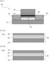
- FIG. 1 is a schematic sectional view of a SiGe channel field effect transistor 10.
- the field effect transistor 10 comprises a substrate 11, a channel region 12 arranged on the substrate 11, drain and source regions 13-14 arranged on the substrate 11 on either side of the channel region 12 , a gate oxide layer 15 provided on the channel region 12 and a gate electrode 16 provided on the gate oxide layer 15.
- the gate electrode 16 is separated from the channel region 12 by the layer of gate oxide 15.
- the field effect transistor 10 is advantageously of the PMOS type.
- the drain and source regions 13-14 are then P-type doped semiconductor regions.
- the channel region 12 comprises an active layer 23 made of silicon-germanium (SiGe), in contact with the gate oxide layer 15.
- This active layer 23 of SiGe can be stressed in compression or, on the contrary, relaxed, i.e. that is to say subject to no stress in tension or compression. It presents in its thickness a germanium concentration gradient.
- the germanium concentration increases as it approaches the interface between the active layer 23 and the gate oxide layer 15 and reaches a maximum value at this interface.
- the maximum value of the germanium concentration is advantageously between 30% and 80% (in atomic percentage) to confer high mobility to the electrical charge carriers in channel region 12 and reduce the threshold voltage of the transistor.
- the gate oxide layer 15 preferably has a thickness of between 0.5 nm and 6 nm.
- the field effect transistor 10 may also comprise a layer of dielectric material with a high dielectric constant (not shown) disposed between the gate oxide layer 15 and the gate electrode 16.
- a dielectric material with a high dielectric constant designates a material having a dielectric constant k greater than the dielectric constant of silicon dioxide (SiO 2 ), i.e. greater than 3.9.
- FIGS. 2A to 2C represent steps S11 to S13 of a method of manufacturing the field effect transistor 10, according to a first mode of implementation of the invention. These steps relate to the formation of the active layer 23 in SiGe (forming the channel region 12) and the gate oxide layer 15.
- Step S11 of the Figure 2A consists of providing a stack 20 comprising the substrate 11, a first layer 21 of SiGe placed on the substrate 11 and a second layer 22 of silicon placed on the first layer 21.
- Substrate 11 may be a bulk substrate made of a semiconductor material (for example silicon, germanium, silicon-germanium or silicon carbide) or a silicon-on-insulator (or SOI) type substrate. On Insulator).
- a semiconductor material for example silicon, germanium, silicon-germanium or silicon carbide
- SOI silicon-on-insulator
- the first layer 21 in SiGe is preferably formed by epitaxy on one face of the substrate 11.
- the first layer 21 in SiGe advantageously has a germanium concentration (also called atomic percentage of germanium) of between 1% and 80%, preferably between 5 % and 60% and even more preferably between 10% and 60%. The higher the percentage of germanium, the smaller the number of defects that can capture holes accumulated in the SiGe film.
- the thickness of the first SiGe layer 21 can be between 5 nm and 50 nm.
- the first SiGe layer 21 does not present a Ge concentration gradient after step S11.
- the second Si layer 22 can also be formed by epitaxy on the first layer 21. Its thickness is preferably between 0.2 nm and 15 nm, preferably between 0.8 nm to 6 nm.
- the gate oxide layer 15 of the transistor is formed on the stack 10, for example by thermal oxidation of at least a portion of the second layer 22.
- the thermal oxidation of the second silicon layer 22 makes it possible to easily obtain a gate oxide layer 15 made of silicon dioxide (SiO 2 ) and having a low defect density, in other words a high quality gate oxide layer 15.
- the gate oxide layer 15 is of high quality when it has a density of interface states Dit less than 2 ⁇ 10 11 /cm 2 /eV.
- a high-quality gate oxide layer prevents degradation of charge carrier mobility in the channel region of the transistor and therefore leads to better current performance.
- Thermal oxidation is carried out by introducing the stack 20 into the chamber of a furnace (for example constituted by a quartz tube), by injecting into the chamber a gas containing oxygen (for example dioxygen) and optionally a neutral gas (such as dinitrogen, N 2 ), then heating the stack 20 to a temperature between 400°C and 1200°C, preferably between 400°C and 500°C.
- a gas containing oxygen for example dioxygen
- a neutral gas such as dinitrogen, N 2
- the gate oxide layer 15 of the transistor is formed by exposing the second layer 22 to a plasma containing oxygen, for example an H 2 O plasma.
- the plasma is preferably formed (in the oxygen chamber). a reactor) at a temperature less than or equal to 500 °C.
- the gate oxide layer 15 is formed by thermal oxidation using nanosecond type laser annealing in the presence of oxygen (typically O 2 ).
- the gate oxide layer 15 is formed by chemical oxidation, for example in an HF + Os bath or under ammonia NH 4 OH + H 2 O 2 .
- a significant thickness of the second Si layer 22 makes it possible to achieve partial oxidation of the second layer 22, whereas with a low thickness, the second layer 22 will be completely oxidized.
- the oxide layer 15 can be subjected to a nitriding post-treatment, for example by annealing under NH 3 at 650°C in an oven, or by a plasma nitriding treatment in the chamber of a reactor. at a temperature less than or equal to 500°C.
- a nitriding post-treatment for example by annealing under NH 3 at 650°C in an oven, or by a plasma nitriding treatment in the chamber of a reactor. at a temperature less than or equal to 500°C.
- the stack 20 is subjected to laser annealing so as to melt a region of the stack 20, this region comprising at least part of the second layer 22 and at least part of the first layer 21, and optionally a part of the substrate 11. Then, while cooling, the molten region of the stack 20 recrystallizes to form the active layer 23 comprising a germanium concentration gradient.
- the germanium concentration gradient of the active layer 23 results from a redistribution of the germanium atoms of the first layer 21 in SiGe, during the melting and recrystallization of the stack region 20.
- the germanium atoms are concentrated in the upper part of the stack 20, at the interface with the gate oxide layer 15.
- the electrical charge carriers of the field effect transistor 10 will benefit from high mobility in the channel region 12 .
- the thickness of the molten region can vary as a function of the initial germanium concentration of the first layer 21 and as a function of the gradient that one seeks to obtain. For example, if we wish to obtain a concentration of approximately 80% at the interface with the gate oxide layer 15 and obtain a gradient between the interface with the gate oxide layer 15 and the first ten nanometers of the first layer 21, while the first layer 21 has a thickness of 30 nm with a concentration of 40% in Ge, then the thickness of the molten region will be approximately 45 nm (corresponding to an energy density of 2.2 J/cm 2 for 160 ns and a wavelength of 308 nm). The thickness of the molten region is advantageously greater than or equal to 15 nm, in order to minimize crystal defects.
- the initial germanium concentration of the first layer 21 and the thickness of the molten region are chosen so as to obtain a maximum germanium concentration at the interface with the layer 21.
- gate oxide 15 between 30% and 80%.
- Laser annealing is accomplished by exposing the surface of gate oxide layer 15 to radiation emitted by a laser source. Thus, the laser radiation passes through the gate oxide layer 15. This is, however, not altered by the laser radiation. It is neither melted nor damaged.
- the laser radiation advantageously has a wavelength of between 200 nm and 600 nm (for example equal to 248 nm, 308 nm or 532 nm) and an energy density of between 0.1 J/cm 2 and 10 J/ cm 2 , preferably between 1.7 J/cm 2 and 2.5 J/cm 2 .
- the duration of exposure to laser radiation can be between 10 ns and 1000 ns (width at half height of the pulse).
- nanosecond laser annealing or NLA, for Nanosecond Laser Annealing
- laser annealing is carried out using an XeCl gas laser with a wavelength equal to 308 nm at an energy density of between 1.7 and 3 J/cm 2 for a duration of 160 ns (width at half maximum).
- the active layer 23 finds itself placed between the gate oxide layer 15 and the remaining part of the first layer 21.
- the first layer 21 can be completely melted during laser annealing.
- the active layer 23 then extends from the substrate 11 to the gate oxide layer 15. A part of the substrate 11 can also be melted.
- FIGS. 3A to 3C represent steps S21 to S23 of a method of manufacturing the field effect transistor 10, according to a second mode of implementation of the invention.
- This second mode of implementation differs from the first mode of implementation only in the constitution of the starting stack.
- the stack 20' provided comprises the substrate 11 and a silicon-germanium layer 21' placed on the substrate 11.
- the stack 20' is devoid of the second silicon layer 22.
- the SiGe layer 21' has a Ge concentration of between 5% and 10%.
- the gate oxide layer 15 is formed on the stack 20', by thermal oxidation of at least part of the SiGe layer 21' (rather than the second Si layer 22) or by exposure of the layer of SiGe 21' to a plasma containing oxygen.
- the gate oxide layer 15 essentially comprises silicon dioxide (it is composed of more than 90% SiO 2 ). Due to the low germanium concentration of the SiGe layer 21', the gate oxide layer 15 contains a small proportion of germanium oxide (GeO x ), typically less than or equal to 10%. The gate oxide layer 15 is then of a higher quality than that obtained by the method of the prior art and does not affect the performance of the transistor.
- a region of the stack 20' is melted by laser annealing then recrystallized to form the active layer 23.
- the region of the stack 20' melted by the laser here comprises all or part of the SiGe layer 21', and possibly part of the substrate 11.
- the laser annealing is preferably accomplished in the manner described in relation to the Figure 2C .
- the thickness of the molten region is advantageously greater than or equal to 15 nm, in order to minimize crystal defects.
- the initial germanium concentration of the SiGe 21' layer and the thickness of the molten region are chosen so as to obtain a maximum germanium concentration at the interface with the gate oxide layer 15 between 30% and 80%.
- the gate oxide layer 15 is preferably formed in step S12/22 in such a way as to have a percentage of germanium oxide (GeO x ) less than or equal to 10% and advantageously zero.
- Laser annealing can be accomplished under an atmosphere devoid of oxygen, typically neutral (for example under N 2 ), so as not to increase the thickness of the gate oxide layer 15 already formed.
- the gate oxide layer 15 is formed during the laser annealing step S13 or S23 (and more particularly during the melting/recrystallization operation) by adding oxygen (typical O 2 ) to the annealing atmosphere.
- oxygen typically O 2
- Laser annealing can be accomplished using a single radiation pulse or multiple successive radiation pulses (received at the same location). This is valid for the two modes of implementing the method (step S13 or S23), with or without simultaneous formation of the gate oxide layer 15.
- the manufacturing process may include a step of depositing a layer of “high-k” dielectric material on the gate oxide layer 15.
- the “high-k” dielectric material -k” is for example hafnium oxide (HfO 2 ).
- the thickness of the layer of “high-k” dielectric material can be between 0.5 nm and 5 nm, preferably between 2 nm and 3 nm.
- the layer of “high-k” dielectric material can be deposited before step S13 or S23 of laser annealing and recrystallization of the active layer 23, to the extent that this layer of “high-k” dielectric material is not affected by laser annealing (like the gate oxide layer 15).
- the layer of “high-k” dielectric material can also be deposited after laser annealing step S13 or S23.
- the manufacturing process can also include a step of forming the gate electrode 16 and a step of forming the drain and source regions 13-14 after obtaining the active layer 23 (therefore after laser annealing). How these steps are accomplished may depend on the type of field effect transistor desired: single-gate MOSFET or multiple-gate MOSFET (FinFET, GAAFET), solid-substrate transistors, or partially or completely silicon-on-insulator transistors. depleted (PDSOI, FDSOI).
- the manufacturing process may comprise, rather than the ion implantation step, an etching of the active layer 23 and an epitaxy step of doped silicon-germanium or doped silicon to form the drain and source regions 13- 14 (FDSOI transistors in particular). It can also include a final annealing step called “forming” aimed at reducing the density of interface states (Dit), preferably at a temperature less than or equal to 500 ° C.
- forming aimed at reducing the density of interface states (Dit), preferably at a temperature less than or equal to 500 ° C.
- This manufacturing process is particularly advantageous in the case of 3D integration (sequential or monolithic) of field effect transistors, because nanosecond laser annealing does not damage the previously formed transistors (respecting the thermal budget of these transistors).
Landscapes
- Thin Film Transistor (AREA)
- Insulated Gate Type Field-Effect Transistor (AREA)
- Physics & Mathematics (AREA)
- Electromagnetism (AREA)
- Optics & Photonics (AREA)
Applications Claiming Priority (1)
| Application Number | Priority Date | Filing Date | Title |
|---|---|---|---|
| FR2213226A FR3143187B1 (fr) | 2022-12-13 | 2022-12-13 | Procédé de fabrication d’un transistor à effet de champ à canal sige |
Publications (3)
| Publication Number | Publication Date |
|---|---|
| EP4386815A2 true EP4386815A2 (de) | 2024-06-19 |
| EP4386815A3 EP4386815A3 (de) | 2024-07-10 |
| EP4386815B1 EP4386815B1 (de) | 2025-11-12 |
Family
ID=86332396
Family Applications (1)
| Application Number | Title | Priority Date | Filing Date |
|---|---|---|---|
| EP23215728.9A Active EP4386815B1 (de) | 2022-12-13 | 2023-12-12 | Verfahren zur herstellung eines sige-kanal-feldeffekttransistors |
Country Status (3)
| Country | Link |
|---|---|
| US (1) | US20240194485A1 (de) |
| EP (1) | EP4386815B1 (de) |
| FR (1) | FR3143187B1 (de) |
Families Citing this family (1)
| Publication number | Priority date | Publication date | Assignee | Title |
|---|---|---|---|---|
| US20240304671A1 (en) * | 2023-03-07 | 2024-09-12 | Applied Materials, Inc. | Methods For Forming Gate Structures |
Citations (1)
| Publication number | Priority date | Publication date | Assignee | Title |
|---|---|---|---|---|
| US20180076040A1 (en) | 2016-09-12 | 2018-03-15 | International Business Machines Corporation | Formation of pure silicon oxide interfacial layer on silicon-germanium channel field effect transistor device |
Family Cites Families (8)
| Publication number | Priority date | Publication date | Assignee | Title |
|---|---|---|---|---|
| US6743680B1 (en) * | 2000-06-22 | 2004-06-01 | Advanced Micro Devices, Inc. | Process for manufacturing transistors having silicon/germanium channel regions |
| US6783591B1 (en) * | 2002-08-06 | 2004-08-31 | Advanced Micro Devices, Inc. | Laser thermal annealing method for high dielectric constant gate oxide films |
| US7579636B2 (en) * | 2004-01-08 | 2009-08-25 | Nec Corporation | MIS-type field-effect transistor |
| US7078302B2 (en) * | 2004-02-23 | 2006-07-18 | Applied Materials, Inc. | Gate electrode dopant activation method for semiconductor manufacturing including a laser anneal |
| KR101817131B1 (ko) * | 2012-03-19 | 2018-01-11 | 에스케이하이닉스 주식회사 | 게이트절연층 형성 방법 및 반도체장치 제조 방법 |
| US11296227B2 (en) * | 2019-10-16 | 2022-04-05 | Taiwan Semiconductor Manufacturing Co., Ltd. | Method of manufacturing semiconductor devices and semiconductor devices |
| CN114256346A (zh) * | 2020-09-21 | 2022-03-29 | 上海华力集成电路制造有限公司 | 一种fdsoi器件结构及其制备方法 |
| CN113299548A (zh) * | 2021-04-23 | 2021-08-24 | 上海华力集成电路制造有限公司 | 栅极电介质层制备方法 |
-
2022
- 2022-12-13 FR FR2213226A patent/FR3143187B1/fr active Active
-
2023
- 2023-12-12 EP EP23215728.9A patent/EP4386815B1/de active Active
- 2023-12-13 US US18/538,292 patent/US20240194485A1/en active Pending
Patent Citations (1)
| Publication number | Priority date | Publication date | Assignee | Title |
|---|---|---|---|---|
| US20180076040A1 (en) | 2016-09-12 | 2018-03-15 | International Business Machines Corporation | Formation of pure silicon oxide interfacial layer on silicon-germanium channel field effect transistor device |
Non-Patent Citations (1)
| Title |
|---|
| L. DAGAULT ET AL., APPLIED SURFACE SCIENCE, vol. 527, 2020 |
Also Published As
| Publication number | Publication date |
|---|---|
| EP4386815A3 (de) | 2024-07-10 |
| FR3143187B1 (fr) | 2026-02-13 |
| EP4386815B1 (de) | 2025-11-12 |
| US20240194485A1 (en) | 2024-06-13 |
| FR3143187A1 (fr) | 2024-06-14 |
Similar Documents
| Publication | Publication Date | Title |
|---|---|---|
| EP1837916B1 (de) | Verfahren zum Herstellen eines Transistors mit einem Germanium enthaltenden Kanal | |
| EP0298794B1 (de) | Verfahren zur Herstellung einer vergrabenen isolierenden Schicht in einem Halbleitersubstrat durch Ionenimplantation und Halbleiterstruktur mit einer solchen Schicht | |
| FR3060840A1 (fr) | Procede de realisation d'un dispositif semi-conducteur a espaceurs internes auto-alignes | |
| FR2465317A2 (fr) | Transistor a effet de champ a frequence de coupure elevee | |
| CN101060134A (zh) | Mosfet器件及其制造方法 | |
| EP1091417A1 (de) | Herstellungsverfahren für Halbleiterbauelement mit Rundherum-Gate und dadurch hergestelltes Bauelement | |
| FR2892230A1 (fr) | Traitement d'une couche de germamium | |
| FR2483127A1 (fr) | Procede de fabrication d'un dispositif semi-conducteur | |
| FR2806832A1 (fr) | Transistor mos a source et drain metalliques, et procede de fabrication d'un tel transistor | |
| EP3079168A1 (de) | Dotierverfahren von source- und drain-bereichen eines transistors mithilfe einer selektiven amorphisierung | |
| EP3142151B1 (de) | Herstellungsverfahren einer einachsig verspannten transistorkanalstruktur | |
| EP4386815B1 (de) | Verfahren zur herstellung eines sige-kanal-feldeffekttransistors | |
| EP0635880B1 (de) | Verfahren zur Herstellung eines Transistors in Silizium-auf-Isolator Technologie | |
| EP3026712B1 (de) | Verbessertes verfahren zur spannungsinduktion einer transistorkanalzone | |
| FR3048816A1 (fr) | Procede de fabrication d'un dispositif avec transistor nmos contraint en tension et transistor pmos contraint en compression uni-axiale | |
| FR3051972A1 (fr) | Procede de realisation d'un transistor comprenant des source et drain obtenus par recristallisation de semi-conducteur | |
| FR2957458A1 (fr) | Procede de realisation d’une electrode conductrice | |
| EP3671826B1 (de) | Verbessertes herstellungsverfahren eines integrierten schaltkreises, der einen nmos- und einen pmos-transistor umfasst | |
| FR2791178A1 (fr) | NOUVEAU DISPOSITIF SEMI-CONDUCTEUR COMBINANT LES AVANTAGES DES ARCHITECTURES MASSIVE ET soi, ET PROCEDE DE FABRICATION | |
| EP2731141A1 (de) | Verfahren zum Herstellung eines Feldeffekttransistors mit einem SiGe-Kanal unter Verwendung von Ionenimplantation | |
| EP3961721A1 (de) | Verbessertes verfahren zur germaniumanreicherung um den kanal eines transistors | |
| EP4386812B1 (de) | Verfahren zur herstellung einer halbleitervorrichtung | |
| EP3859769B1 (de) | Verfahren zum ätzen im nanometerbereich einer germanium-zinn-legierung (gesn) für fet-transistor | |
| FR2791181A1 (fr) | Nouveaux transistor a grille metallique et canal enterre, contre-dope, et procede de fabrication | |
| EP1033748A1 (de) | Neuer SiGe-Legierung Indium-implantiert Transistor und Verfahren zur dessen Herstellung |
Legal Events
| Date | Code | Title | Description |
|---|---|---|---|
| PUAI | Public reference made under article 153(3) epc to a published international application that has entered the european phase |
Free format text: ORIGINAL CODE: 0009012 |
|
| STAA | Information on the status of an ep patent application or granted ep patent |
Free format text: STATUS: REQUEST FOR EXAMINATION WAS MADE |
|
| PUAL | Search report despatched |
Free format text: ORIGINAL CODE: 0009013 |
|
| 17P | Request for examination filed |
Effective date: 20231212 |
|
| AK | Designated contracting states |
Kind code of ref document: A2 Designated state(s): AL AT BE BG CH CY CZ DE DK EE ES FI FR GB GR HR HU IE IS IT LI LT LU LV MC ME MK MT NL NO PL PT RO RS SE SI SK SM TR |
|
| AK | Designated contracting states |
Kind code of ref document: A3 Designated state(s): AL AT BE BG CH CY CZ DE DK EE ES FI FR GB GR HR HU IE IS IT LI LT LU LV MC ME MK MT NL NO PL PT RO RS SE SI SK SM TR |
|
| RIC1 | Information provided on ipc code assigned before grant |
Ipc: H01L 29/10 20060101ALI20240605BHEP Ipc: H01L 29/51 20060101ALI20240605BHEP Ipc: H01L 21/336 20060101AFI20240605BHEP |
|
| RAP3 | Party data changed (applicant data changed or rights of an application transferred) |
Owner name: COMMISSARIAT A L'ENERGIE ATOMIQUE ET AUX ENERGIESALTERNATIVES |
|
| REG | Reference to a national code |
Ref country code: DE Ref legal event code: R079 Free format text: PREVIOUS MAIN CLASS: H01L0021336000 Ipc: H10D0030010000 Ref country code: DE Ref legal event code: R079 Ref document number: 602023008531 Country of ref document: DE Free format text: PREVIOUS MAIN CLASS: H01L0021336000 Ipc: H10D0030010000 |
|
| GRAP | Despatch of communication of intention to grant a patent |
Free format text: ORIGINAL CODE: EPIDOSNIGR1 |
|
| STAA | Information on the status of an ep patent application or granted ep patent |
Free format text: STATUS: GRANT OF PATENT IS INTENDED |
|
| RIC1 | Information provided on ipc code assigned before grant |
Ipc: H01L 21/28 20060101ALI20250514BHEP Ipc: H01L 21/268 20060101ALI20250514BHEP Ipc: H10D 64/68 20250101ALI20250514BHEP Ipc: H10D 30/60 20250101ALI20250514BHEP Ipc: H10D 30/01 20250101AFI20250514BHEP |
|
| INTG | Intention to grant announced |
Effective date: 20250610 |
|
| GRAS | Grant fee paid |
Free format text: ORIGINAL CODE: EPIDOSNIGR3 |
|
| GRAA | (expected) grant |
Free format text: ORIGINAL CODE: 0009210 |
|
| STAA | Information on the status of an ep patent application or granted ep patent |
Free format text: STATUS: THE PATENT HAS BEEN GRANTED |
|
| AK | Designated contracting states |
Kind code of ref document: B1 Designated state(s): AL AT BE BG CH CY CZ DE DK EE ES FI FR GB GR HR HU IE IS IT LI LT LU LV MC ME MK MT NL NO PL PT RO RS SE SI SK SM TR |
|
| REG | Reference to a national code |
Ref country code: CH Ref legal event code: F10 Free format text: ST27 STATUS EVENT CODE: U-0-0-F10-F00 (AS PROVIDED BY THE NATIONAL OFFICE) Effective date: 20251112 Ref country code: GB Ref legal event code: FG4D Free format text: NOT ENGLISH |
|
| REG | Reference to a national code |
Ref country code: DE Ref legal event code: R096 Ref document number: 602023008531 Country of ref document: DE |
|
| REG | Reference to a national code |
Ref country code: IE Ref legal event code: FG4D Free format text: LANGUAGE OF EP DOCUMENT: FRENCH |
|
| PGFP | Annual fee paid to national office [announced via postgrant information from national office to epo] |
Ref country code: AT Payment date: 20260113 Year of fee payment: 3 |
|
| REG | Reference to a national code |
Ref country code: NL Ref legal event code: MP Effective date: 20251112 |
|
| PG25 | Lapsed in a contracting state [announced via postgrant information from national office to epo] |
Ref country code: ES Free format text: LAPSE BECAUSE OF FAILURE TO SUBMIT A TRANSLATION OF THE DESCRIPTION OR TO PAY THE FEE WITHIN THE PRESCRIBED TIME-LIMIT Effective date: 20251112 |
|
| REG | Reference to a national code |
Ref country code: LT Ref legal event code: MG9D |
|
| PG25 | Lapsed in a contracting state [announced via postgrant information from national office to epo] |
Ref country code: NO Free format text: LAPSE BECAUSE OF FAILURE TO SUBMIT A TRANSLATION OF THE DESCRIPTION OR TO PAY THE FEE WITHIN THE PRESCRIBED TIME-LIMIT Effective date: 20260212 |
|
| PGFP | Annual fee paid to national office [announced via postgrant information from national office to epo] |
Ref country code: DE Payment date: 20260102 Year of fee payment: 3 |
|
| PG25 | Lapsed in a contracting state [announced via postgrant information from national office to epo] |
Ref country code: AT Free format text: LAPSE BECAUSE OF FAILURE TO SUBMIT A TRANSLATION OF THE DESCRIPTION OR TO PAY THE FEE WITHIN THE PRESCRIBED TIME-LIMIT Effective date: 20251112 Ref country code: HR Free format text: LAPSE BECAUSE OF FAILURE TO SUBMIT A TRANSLATION OF THE DESCRIPTION OR TO PAY THE FEE WITHIN THE PRESCRIBED TIME-LIMIT Effective date: 20251112 Ref country code: FI Free format text: LAPSE BECAUSE OF FAILURE TO SUBMIT A TRANSLATION OF THE DESCRIPTION OR TO PAY THE FEE WITHIN THE PRESCRIBED TIME-LIMIT Effective date: 20251112 |
|
| REG | Reference to a national code |
Ref country code: AT Ref legal event code: MK05 Ref document number: 1857950 Country of ref document: AT Kind code of ref document: T Effective date: 20251112 |
|
| PG25 | Lapsed in a contracting state [announced via postgrant information from national office to epo] |
Ref country code: NL Free format text: LAPSE BECAUSE OF FAILURE TO SUBMIT A TRANSLATION OF THE DESCRIPTION OR TO PAY THE FEE WITHIN THE PRESCRIBED TIME-LIMIT Effective date: 20251112 |
|
| PG25 | Lapsed in a contracting state [announced via postgrant information from national office to epo] |
Ref country code: RS Free format text: LAPSE BECAUSE OF FAILURE TO SUBMIT A TRANSLATION OF THE DESCRIPTION OR TO PAY THE FEE WITHIN THE PRESCRIBED TIME-LIMIT Effective date: 20260212 |
|
| PG25 | Lapsed in a contracting state [announced via postgrant information from national office to epo] |
Ref country code: IS Free format text: LAPSE BECAUSE OF FAILURE TO SUBMIT A TRANSLATION OF THE DESCRIPTION OR TO PAY THE FEE WITHIN THE PRESCRIBED TIME-LIMIT Effective date: 20260312 |
|
| PGFP | Annual fee paid to national office [announced via postgrant information from national office to epo] |
Ref country code: FR Payment date: 20260107 Year of fee payment: 3 |
|
| PG25 | Lapsed in a contracting state [announced via postgrant information from national office to epo] |
Ref country code: PT Free format text: LAPSE BECAUSE OF FAILURE TO SUBMIT A TRANSLATION OF THE DESCRIPTION OR TO PAY THE FEE WITHIN THE PRESCRIBED TIME-LIMIT Effective date: 20260312 |
|
| PG25 | Lapsed in a contracting state [announced via postgrant information from national office to epo] |
Ref country code: PL Free format text: LAPSE BECAUSE OF FAILURE TO SUBMIT A TRANSLATION OF THE DESCRIPTION OR TO PAY THE FEE WITHIN THE PRESCRIBED TIME-LIMIT Effective date: 20251112 |
|
| PG25 | Lapsed in a contracting state [announced via postgrant information from national office to epo] |
Ref country code: LV Free format text: LAPSE BECAUSE OF FAILURE TO SUBMIT A TRANSLATION OF THE DESCRIPTION OR TO PAY THE FEE WITHIN THE PRESCRIBED TIME-LIMIT Effective date: 20251112 |