EP4383348A1 - Passivierungskontaktstruktur und herstellungsverfahren dafür sowie solarzelle damit - Google Patents
Passivierungskontaktstruktur und herstellungsverfahren dafür sowie solarzelle damit Download PDFInfo
- Publication number
- EP4383348A1 EP4383348A1 EP22852364.3A EP22852364A EP4383348A1 EP 4383348 A1 EP4383348 A1 EP 4383348A1 EP 22852364 A EP22852364 A EP 22852364A EP 4383348 A1 EP4383348 A1 EP 4383348A1
- Authority
- EP
- European Patent Office
- Prior art keywords
- conductive film
- transparent conductive
- passivation
- contact structure
- layer
- Prior art date
- Legal status (The legal status is an assumption and is not a legal conclusion. Google has not performed a legal analysis and makes no representation as to the accuracy of the status listed.)
- Withdrawn
Links
Images


Classifications
-
- H—ELECTRICITY
- H10—SEMICONDUCTOR DEVICES; ELECTRIC SOLID-STATE DEVICES NOT OTHERWISE PROVIDED FOR
- H10F—INORGANIC SEMICONDUCTOR DEVICES SENSITIVE TO INFRARED RADIATION, LIGHT, ELECTROMAGNETIC RADIATION OF SHORTER WAVELENGTH OR CORPUSCULAR RADIATION
- H10F77/00—Constructional details of devices covered by this subclass
- H10F77/30—Coatings
- H10F77/306—Coatings for devices having potential barriers
- H10F77/311—Coatings for devices having potential barriers for photovoltaic cells
-
- H—ELECTRICITY
- H10—SEMICONDUCTOR DEVICES; ELECTRIC SOLID-STATE DEVICES NOT OTHERWISE PROVIDED FOR
- H10F—INORGANIC SEMICONDUCTOR DEVICES SENSITIVE TO INFRARED RADIATION, LIGHT, ELECTROMAGNETIC RADIATION OF SHORTER WAVELENGTH OR CORPUSCULAR RADIATION
- H10F10/00—Individual photovoltaic cells, e.g. solar cells
- H10F10/10—Individual photovoltaic cells, e.g. solar cells having potential barriers
- H10F10/14—Photovoltaic cells having only PN homojunction potential barriers
-
- H—ELECTRICITY
- H10—SEMICONDUCTOR DEVICES; ELECTRIC SOLID-STATE DEVICES NOT OTHERWISE PROVIDED FOR
- H10F—INORGANIC SEMICONDUCTOR DEVICES SENSITIVE TO INFRARED RADIATION, LIGHT, ELECTROMAGNETIC RADIATION OF SHORTER WAVELENGTH OR CORPUSCULAR RADIATION
- H10F10/00—Individual photovoltaic cells, e.g. solar cells
- H10F10/10—Individual photovoltaic cells, e.g. solar cells having potential barriers
- H10F10/16—Photovoltaic cells having only PN heterojunction potential barriers
- H10F10/164—Photovoltaic cells having only PN heterojunction potential barriers comprising heterojunctions with Group IV materials, e.g. ITO/Si or GaAs/SiGe photovoltaic cells
- H10F10/165—Photovoltaic cells having only PN heterojunction potential barriers comprising heterojunctions with Group IV materials, e.g. ITO/Si or GaAs/SiGe photovoltaic cells the heterojunctions being Group IV-IV heterojunctions, e.g. Si/Ge, SiGe/Si or Si/SiC photovoltaic cells
- H10F10/166—Photovoltaic cells having only PN heterojunction potential barriers comprising heterojunctions with Group IV materials, e.g. ITO/Si or GaAs/SiGe photovoltaic cells the heterojunctions being Group IV-IV heterojunctions, e.g. Si/Ge, SiGe/Si or Si/SiC photovoltaic cells the Group IV-IV heterojunctions being heterojunctions of crystalline and amorphous materials, e.g. silicon heterojunction [SHJ] photovoltaic cells
-
- H—ELECTRICITY
- H10—SEMICONDUCTOR DEVICES; ELECTRIC SOLID-STATE DEVICES NOT OTHERWISE PROVIDED FOR
- H10F—INORGANIC SEMICONDUCTOR DEVICES SENSITIVE TO INFRARED RADIATION, LIGHT, ELECTROMAGNETIC RADIATION OF SHORTER WAVELENGTH OR CORPUSCULAR RADIATION
- H10F71/00—Manufacture or treatment of devices covered by this subclass
- H10F71/129—Passivating
-
- H—ELECTRICITY
- H10—SEMICONDUCTOR DEVICES; ELECTRIC SOLID-STATE DEVICES NOT OTHERWISE PROVIDED FOR
- H10F—INORGANIC SEMICONDUCTOR DEVICES SENSITIVE TO INFRARED RADIATION, LIGHT, ELECTROMAGNETIC RADIATION OF SHORTER WAVELENGTH OR CORPUSCULAR RADIATION
- H10F77/00—Constructional details of devices covered by this subclass
- H10F77/20—Electrodes
- H10F77/206—Electrodes for devices having potential barriers
- H10F77/211—Electrodes for devices having potential barriers for photovoltaic cells
- H10F77/219—Arrangements for electrodes of back-contact photovoltaic cells
-
- H—ELECTRICITY
- H10—SEMICONDUCTOR DEVICES; ELECTRIC SOLID-STATE DEVICES NOT OTHERWISE PROVIDED FOR
- H10F—INORGANIC SEMICONDUCTOR DEVICES SENSITIVE TO INFRARED RADIATION, LIGHT, ELECTROMAGNETIC RADIATION OF SHORTER WAVELENGTH OR CORPUSCULAR RADIATION
- H10F77/00—Constructional details of devices covered by this subclass
- H10F77/20—Electrodes
- H10F77/244—Electrodes made of transparent conductive layers, e.g. transparent conductive oxide [TCO] layers
- H10F77/247—Electrodes made of transparent conductive layers, e.g. transparent conductive oxide [TCO] layers comprising indium tin oxide [ITO]
-
- H—ELECTRICITY
- H10—SEMICONDUCTOR DEVICES; ELECTRIC SOLID-STATE DEVICES NOT OTHERWISE PROVIDED FOR
- H10F—INORGANIC SEMICONDUCTOR DEVICES SENSITIVE TO INFRARED RADIATION, LIGHT, ELECTROMAGNETIC RADIATION OF SHORTER WAVELENGTH OR CORPUSCULAR RADIATION
- H10F77/00—Constructional details of devices covered by this subclass
- H10F77/20—Electrodes
- H10F77/244—Electrodes made of transparent conductive layers, e.g. transparent conductive oxide [TCO] layers
- H10F77/251—Electrodes made of transparent conductive layers, e.g. transparent conductive oxide [TCO] layers comprising zinc oxide [ZnO]
-
- H—ELECTRICITY
- H10—SEMICONDUCTOR DEVICES; ELECTRIC SOLID-STATE DEVICES NOT OTHERWISE PROVIDED FOR
- H10F—INORGANIC SEMICONDUCTOR DEVICES SENSITIVE TO INFRARED RADIATION, LIGHT, ELECTROMAGNETIC RADIATION OF SHORTER WAVELENGTH OR CORPUSCULAR RADIATION
- H10F77/00—Constructional details of devices covered by this subclass
- H10F77/30—Coatings
- H10F77/306—Coatings for devices having potential barriers
- H10F77/311—Coatings for devices having potential barriers for photovoltaic cells
- H10F77/315—Coatings for devices having potential barriers for photovoltaic cells the coatings being antireflective or having enhancing optical properties
-
- Y—GENERAL TAGGING OF NEW TECHNOLOGICAL DEVELOPMENTS; GENERAL TAGGING OF CROSS-SECTIONAL TECHNOLOGIES SPANNING OVER SEVERAL SECTIONS OF THE IPC; TECHNICAL SUBJECTS COVERED BY FORMER USPC CROSS-REFERENCE ART COLLECTIONS [XRACs] AND DIGESTS
- Y02—TECHNOLOGIES OR APPLICATIONS FOR MITIGATION OR ADAPTATION AGAINST CLIMATE CHANGE
- Y02E—REDUCTION OF GREENHOUSE GAS [GHG] EMISSIONS, RELATED TO ENERGY GENERATION, TRANSMISSION OR DISTRIBUTION
- Y02E10/00—Energy generation through renewable energy sources
- Y02E10/50—Photovoltaic [PV] energy
-
- Y—GENERAL TAGGING OF NEW TECHNOLOGICAL DEVELOPMENTS; GENERAL TAGGING OF CROSS-SECTIONAL TECHNOLOGIES SPANNING OVER SEVERAL SECTIONS OF THE IPC; TECHNICAL SUBJECTS COVERED BY FORMER USPC CROSS-REFERENCE ART COLLECTIONS [XRACs] AND DIGESTS
- Y02—TECHNOLOGIES OR APPLICATIONS FOR MITIGATION OR ADAPTATION AGAINST CLIMATE CHANGE
- Y02P—CLIMATE CHANGE MITIGATION TECHNOLOGIES IN THE PRODUCTION OR PROCESSING OF GOODS
- Y02P70/00—Climate change mitigation technologies in the production process for final industrial or consumer products
- Y02P70/50—Manufacturing or production processes characterised by the final manufactured product
Definitions
- the present invention mainly relates to a solar cell, and in particular to a passivation contact structure and manufacturing method therefor and solar cell using same.
- metal busbars are in direct contact with silicon to collect carriers.
- direct contact between metal and silicon will cause a large amount of additional carrier recombination, resulting in losses.
- passivation contact the concept of which is that one type of carrier is blocked by the tunnel layer at the front end of the metal contact, so no relevant recombination occurs at the metal contact interface.
- the tunnel layer is passivated, which means that the tunnel layer will not cause a large amount of carrier recombination, thereby achieving the effect of only a small amount of recombination loss during metal contact.
- the traditional passivation contact structure generally contains amorphous silicon, and this polycrystalline layer using silicon material mostly absorbs light seriously, as a result, the existing passivation contact structure not only reduces the recombination loss caused by the direct contact between the metal busbar and silicon, but also generates parasitic light absorption loss. Therefore, on the whole, the traditional passivation contact structure placed on the front side does not have a very good effect on improving the energy conversion performance of solar cells.
- the technical problem to be solved by the present invention is to provide a passivation contact structure and manufacturing method therefor and solar cell using same, and both electricity conducting and passivation effects can be achieved, and the effect of reducing the loss of light absorption can also be achieved.
- the present application provides a passivation contact structure for a solar cell, comprising: a tunnel layer; a transparent conductive film, located on the tunnel layer and in contact with the tunnel layer; a cover layer, located on the transparent conductive film; and a metal electrode, passing through the cover layer to be in contact with the transparent conductive film, and an end surface of metal electrode being located in the transparent conductive film.
- the transparent conductive film is a first doping type transparent conductive film.
- the passivation contact structure further comprising: a substrate; a first semiconductor layer of a first doping type located on the substrate, wherein the tunnel layer is located on the first semiconductor layer.
- the first doping type is N type.
- a thickness of the tunnel layer is between 0.5-3nm.
- a thickness of the transparent conductive film is between 10-300nm.
- a material of the transparent conductive film is one of zinc oxide.
- Another aspect of the present invention also provides a solar cell, comprising the above-mentioned passivation contact structure.
- Another aspect of the present invention also provides a method for manufacturing a passivation contact structure for a solar cell, comprising following steps: forming a tunnel layer; forming a transparent conductive film on the tunnel layer; forming a cover layer on the transparent conductive film; and forming a metal electrode passing through the cover layer to be in contact with the transparent conductive film, and an end surface of the metal electrode being located in the transparent conductive film.
- the method further comprising forming a semiconductor layer of a first doping type on the substrate, wherein the tunnel layer is formed on the semiconductor layer.
- the present invention provides a passivation contact structure and manufacturing method therefor and solar cell using same, which adopts a method of combining a transparent conductive film with a tunnel layer, and both electricity conducting and passivation effects between metal and non-metal areas can be achieved, resulting in effectively reducing carrier recombination losses in silicon-based solar cells.
- the high light transmittance of the transparent conductive film also has the effect of reducing the absorption loss of incident light, thereby improving the energy conversion efficiency of the solar cell as a whole.
- orientation words such as “front, back, up, down, left, right", “ landscape, portrait, vertical, horizontal” and “top, bottom” etc. indicating the orientation or positional relationship is generally based on the orientation or positional relationship shown in the drawings, only for the convenience of describing the application and simplifying the description, in the absence of a contrary statement, these orientation words do not indicate or imply that the device or element referred to must have a specific orientation or be constructed and operated in a specific orientation, and therefore cannot be construed as limiting the scope of protection of this application; the orientation words “inside and outside” refer to inside and outside relative to the outline of each part itself.
- spatially relative terms may be used here, such as “on !, “over !, “on the upper surface of !, “above”, etc., to describe the spatial positional relationship between one device or feature and other devices or features. It will be understood that, in addition to the orientation depicted in the drawings, the spatially relative terms are intended to encompass different orientations of the device in use or operation. For example, if the device in the drawings is turned over, devices described as “on other devices or configurations “ or “above other devices or configurations " would then be oriented “beneath other devices or configurations " or “under other devices or configurations ". Thus, the exemplary term “above” can encompass both an orientation of “above” and “beneath”. The device may be otherwise oriented (rotated 90 degrees or at other orientations), and making a corresponding explanation for the space relative description used here.
- One embodiment of the present invention proposes a passivation contact structure for a solar cell, which combines a transparent conductive film with a tunnel layer; both electricity conducting and passivation effects can be achieved, and the effect of reducing the loss of light absorption can also be achieved.
- Fig.1 shows a schematic structural view of a passivation contact structure10 of a solar cell according to an embodiment of the present invention.
- the passivation contact structure 10 can be used on the front surface or the back surface of the solar cell.
- the passivation contact structure 10 comprises a tunnel layer 11, a transparent conductive film 12, a cover layer 13 and a metal electrode 14 in sequence.
- the tunnel layer 11 can block holes from entering the transparent conductive film 12.
- the tunnel layer can be silicon oxide, but the material of the tunnel layer in the present invention is not limited to this, in other embodiments of the present invention, the tunnel layer can be made of other materials.
- the thickness of the tunnel layer 11 is between 0.5-3 nm.
- the transparent conductive film 12 is located on the tunnel layer 11 and is in direct contact with the tunnel layer 11 without other battery hierarchical structures between them.
- the transparent conductive film 12 is made of zinc oxide.
- the transparent conductive film 12 may also be made of other materials such as silicon oxide and aluminum oxide.
- the thickness of the transparent conductive film 12 is between 10-300 nm.
- the cover layer 13 is located on the transparent conductive film 12.
- the cover layer 13 can play a role in protecting the transparent conductive film 12, and is generally made of silicon nitride, aluminum oxide or other materials.
- the cover layer 13 can protect the transparent conductive film 12 from water vapor, PID (Potential Induced Degradation) ions, physical friction, hydrogen source loss during the sintering process, and metal peeling.
- the metal electrode 14 passes through the cover layer 13 and contacts the transparent conductive film 12, and the end surface 14a of the metal electrode 14 is located in the transparent conductive film 12.
- the material of the metal electrode 14 may be silver, aluminum, copper, etc., and the present invention does not limit the material selection of the metal electrode.
- the degree of metal corrosion is as follows: after the metal electrode 14 passes through the uppermost cover layer 13, it reaches a state that the metal electrode 14 is in contact with the transparent conductive film 12 but does not further reach the tunnel layer 11 or even damage it.
- the transparent conductive film 12 shown in Fig. 1 is a first doping type transparent conductive film.
- the first doping type may be N-type
- the transparent conductive film 12 is an N-type doping transparent conductive film.
- the material of the transparent conductive film 12 is zinc oxide
- an appropriate amount of aluminum can be added to the slurry when manufacturing the passivation contact structure 10. This can enhance the N-type doping of the contact area between zinc oxide and the metal, making it easier for electrons to transmit from the transparent conductive film 12 to the metal electrode 14.
- the transparent conductive film 12 does not need to be highly doped and only needs to provide longitudinal transport of electrons.
- the transparent conductive film 12 accommodates the end surface 14a of the metal electrode 14, which can effectively protect the bottom tunnel layer 11 from damage; after the battery manufacturing is completed, it can also ensure the efficient collection and transmission of electrons inside the battery.
- the high light transmittance capacity because the transparent conductive film does not require very high doping
- the transparent conductive film 12 can effectively solve the impact of light absorption by amorphous silicon and polycrystalline silicon in traditional passivation structures.
- the passivation contact structure 10 also comprises a substrate 15 and a first semiconductor layer 16 using the above-mentioned first doping type, and the first semiconductor layer 16 is located on the substrate 15, and the tunnel layer 11 is located on the first semiconductor layer 16.
- the substrate 15 is made of silicon.
- the first semiconductor layer 16 is an N-type doping semiconductor layer. N-type doping is applied to increase lateral conduction within the substrate 15 (ie, the silicon body) and to form better contact with the transparent conductive film 12.
- the N-type doping first semiconductor layer 16 can be realized by doping with substances such as phosphorus or gallium, which is not limited by the present invention.
- the substrate 15 itself may be P-type doping or N-type doping.
- P-type doping can be achieved by doping boron or gallium
- N-type doping can be achieved by doping phosphorus or arsenic.
- the first semiconductor layer 16 when manufacturing the first semiconductor layer 16, it can be manufactured independently on the substrate 15, or it can be doped and manufactured inside the substrate 15, and the present invention does not limit the manufacturing process. After the manufacturing is completed, an N-type doping first semiconductor layer 16 is formed on the substrate 15 as shown in Fig. 1 .
- the present invention adopts a structure in which a transparent conductive film (such as zinc oxide) is in direct contact with the tunnel layer, and the two can be used in combination to together achieve a passivation effect.
- a transparent conductive film such as zinc oxide
- the transparent conductive film can effectively protect the tunnel layer in direct contact with it from damage, and after the cell manufacturing is completed, it can ensure efficient collection and transmission of electrons.
- the structure in which the transparent conductive film is combined with the tunnel layer avoids serious adverse consequences of light absorption by the polysilicon layer in the existing passivation structure, utilizing the high light transmittance of the transparent conductive film, and the passivation contact structure of the present invention can effectively reduce light absorption loss while providing a passivation contact effect.
- an ellipsometer is applied to compare aluminum-doped ZnO (that is, a transparent conductive film used in a passivation contact structure of a solar cell according to an embodiment of the present invention) with polysilicon that provides passivation contact for traditional solar cells, at the same wavelength of 632nm, the extinction coefficient of aluminum-doped ZnO is about 0.017, and that of polysilicon is 0.252.It can be seen from this that the use of the passivation contact structure of the present invention can significantly reduce light absorption loss, improving the energy conversion efficiency of solar cells, and optimizing the performance of solar cells.
- an embodiment of the present invention also provides a solar cell comprising the above passivation contact structure.
- solar cells with the above passivation contact structure avoid the adverse effects of light absorption by the polysilicon layer and have better energy conversion effects.
- Fig. 2 shows the structure of a TOPerc (the backside structure of a passivation emitter and rear cell (PERC) combined with the frontside structure of a TOPCon cell) solar cell 20 using the passivation contact structure of the invention according to an embodiment of the present invention.
- the solar cell 20 in this embodiment is a P-type substrate cell, but the present invention is not limited to this structure type.
- the upper half of the solar cell 20 (that is, the positive electrode part) adopts a passivation contact structure as shown in Fig. 1 , which specifically comprises a tunnel layer 21, a transparent conductive film 22, and a cover layer 23, front metal electrode 241, P-type substrate 25 and N-type doping first semiconductor layer 26.
- the P-type substrate 25 is a P-type silicon substrate
- the first semiconductor layer 26 is N-type doping (for example, phosphorus doping)
- the tunnel layer 21 is silicon oxide
- the transparent conductive film 22 is made of aluminum-doping zinc oxide
- the cover layer 23 is made of silicon nitride, but the solar cell of the present invention is not limited to such material selection.
- the back side of the solar cell 20 there is also a passivation layer 27, a passivation anti-reflection film 28 and a metal electrode 242 on the back side under the P-type substrate 25.
- the material of the passivation layer 27 is, for example, aluminum oxide
- the material of the passivation anti-reflection film 28 is, for example, silicon nitride.
- the metal electrode 242 on the back its end surface located in the P-type substrate 25 also has an aluminum back field 29.
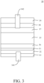
- FIG. 3 it is a schematic structural view of an N-type solar cell using the passivation contact structure of the present invention according to an embodiment of the present invention.
- the back side of the solar cell 30 has the passivation contact structure described above.
- the solar cell 30 has a tunnel layer 31, a transparent conductive film 32, a cover layer 33, a metal electrode 341 on the back, an N-type substrate 35 and an N-type doping first semiconductor layer 36.
- the front side of the solar cell 30 also has a front metal electrode 342, a passivation anti-reflection film 39, a passivation layer 38, and an emitter 37.
- the passivation anti-reflection film 39 is, for example, silicon nitride; the passivation layer is, for example, aluminum oxide; and the emitter 37 is, for example, a boron diffused emitter.
- the N-type substrate 35 is an N-type silicon substrate
- the first semiconductor layer 36 is N-type doping (for example, phosphorus doping)
- the tunnel layer 31 is silicon oxide
- the transparent conductive film 32 is aluminum-doping zinc oxide
- the cover layer 33 is silicon nitride.
- the solar cell of the present invention is not limited to such material selection.
- the above-mentioned solar cell applies the above-mentioned passivation contact structure of the present invention on its front or back side, in which the transparent conductive film has high light transmittance capacity and is used in combination with the tunnel layer; on the basis of providing passivation contact effect, compared with traditional solar cells that use polysilicon as a passivation layer, the above-mentioned passivation contact structure also have the effect of reducing light absorption loss.
- the present invention is not limited to the embodiments shown in Fig.2 and Fig.3 .
- the above-mentioned passivation contact structure can be used on both the front and back sides of the solar cell, thus providing better passivation contact effects in different application scenarios while effectively reducing light absorption loss.
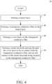
- Another embodiment of the present invention also provides a method for manufacturing the above-mentioned passivation contact structure for a solar cell. As shown in Fig.4 , the method 40 comprises the following steps.
- Step 41 is forming a tunnel layer.
- the tunnel layer can be deposited by a thermal oxygen reaction.
- the deposition temperature is 750°C
- the thickness of the tunnel layer finally formed is 1.5 nm.
- Step 42 is forming a transparent conductive film on the tunnel layer.
- the transparent conductive film is formed by using the ALD method (atomic layer deposition) to deposit a transparent conductive film ZnO on one side of the tunnel layer, the deposition temperature is 200°C, and the thickness of the transparent conductive film finally formed is 60nm.
- ALD method atomic layer deposition
- Step 43 is forming a cover layer on the transparent conductive film.
- the step of preparing the cover layer in step 43 may use a tubular PECVD (Plasma Enhanced Chemical Vapor Deposition) method to prepare SiNx as the cover layer.
- Step 44 is forming a metal electrode passing through the cover layer and to be in contact with the transparent conductive film, and an end surface of the metal electrode being located in the transparent conductive film.
- the method for manufacturing a passivation contact structure for a solar cell further comprises forming a first doping type semiconductor layer on the substrate, and the tunnel layer formed in step 41 will be formed on the semiconductor layer, and the first doping type may be N-type.
- the manufacturing method of the passivation contact structure for solar cells of the present invention please refer to the above description of the passivation contact structure and the solar cell with the passivation contact structure of the present invention, which will not be described again in this part.
- Fig. 4 in this application uses a flow chart to illustrate the operations performed by the system according to the embodiment of this application. It should be understood that the preceding or following operations are not necessarily performed in exact order. Instead, the various steps can be processed in reverse order or simultaneously. At the same time, other operations may be added to these processes, or a step or steps may be removed from these processes.
- the manufacturing method of a TOPerc solar cell taking a P-type substrate cell as an example
- the above passivation contact structure is as follows:
- the manufacturing method of an N-type substrate battery with the above passivation contact structure as an example is as follows:
- numbers describing the quantity of components and attributes are used, it should be understood that such numbers used in the description of the embodiments use the modifiers "about”, “approximately” or “substantially” in some examples. Unless otherwise stated, “about”, “approximately” or “substantially” indicates that the stated figure allows for a variation of ⁇ 20%. Accordingly, in some embodiments, the numerical parameters used in the specification and claims are approximations that can vary depending upon the desired characteristics of individual embodiments. In some embodiments, numerical parameters should take into account the specified significant digits and adopt the general digit reservation method. Although the numerical ranges and parameters used in some embodiments of the present application to confirm the breadth of the scope are approximate values, in specific embodiments, such numerical values are set as precisely as practicable.
Landscapes
- Photovoltaic Devices (AREA)
- Life Sciences & Earth Sciences (AREA)
- Sustainable Development (AREA)
- Engineering & Computer Science (AREA)
- Sustainable Energy (AREA)
Applications Claiming Priority (2)
| Application Number | Priority Date | Filing Date | Title |
|---|---|---|---|
| CN202110897352.1A CN113506832A (zh) | 2021-08-05 | 2021-08-05 | 钝化接触结构、其制备方法以及其应用的太阳能电池 |
| PCT/CN2022/110671 WO2023011653A1 (zh) | 2021-08-05 | 2022-08-05 | 钝化接触结构、其制备方法以及其应用的太阳能电池 |
Publications (2)
| Publication Number | Publication Date |
|---|---|
| EP4383348A1 true EP4383348A1 (de) | 2024-06-12 |
| EP4383348A4 EP4383348A4 (de) | 2024-11-27 |
Family
ID=78015731
Family Applications (1)
| Application Number | Title | Priority Date | Filing Date |
|---|---|---|---|
| EP22852364.3A Withdrawn EP4383348A4 (de) | 2021-08-05 | 2022-08-05 | Passivierungskontaktstruktur und herstellungsverfahren dafür sowie solarzelle damit |
Country Status (6)
| Country | Link |
|---|---|
| US (1) | US20240313132A1 (de) |
| EP (1) | EP4383348A4 (de) |
| JP (1) | JP2024529031A (de) |
| CN (1) | CN113506832A (de) |
| AU (1) | AU2022324515A1 (de) |
| WO (1) | WO2023011653A1 (de) |
Families Citing this family (8)
| Publication number | Priority date | Publication date | Assignee | Title |
|---|---|---|---|---|
| CN113506832A (zh) * | 2021-08-05 | 2021-10-15 | 天合光能股份有限公司 | 钝化接触结构、其制备方法以及其应用的太阳能电池 |
| CN114628534A (zh) * | 2022-03-14 | 2022-06-14 | 天合光能股份有限公司 | 钝化接触的太阳能电池和太阳能电池串 |
| CN115188844B (zh) * | 2022-06-27 | 2025-09-12 | 隆基绿能科技股份有限公司 | 一种太阳能电池及其制备方法、光伏组件 |
| CN116454141B (zh) * | 2023-04-20 | 2024-01-19 | 江苏海洋大学 | 一种应用于晶硅太阳电池的透明导电钝化叠层薄膜及其制备方法 |
| CN117438480A (zh) * | 2023-10-30 | 2024-01-23 | 天合光能股份有限公司 | 透明导电接触钝化的异质结太阳电池及电池组件 |
| CN117995919B (zh) * | 2024-03-29 | 2024-08-16 | 天合光能股份有限公司 | 太阳能电池及其制作方法、光伏组件及光伏系统 |
| CN119153555B (zh) * | 2024-09-18 | 2025-11-28 | 天合光能股份有限公司 | 太阳能电池及其制备方法 |
| CN119562662B (zh) * | 2024-11-25 | 2026-01-06 | 江苏润达新能源科技有限公司 | 一种TOPCon电池膜层结构及其制备方法 |
Family Cites Families (13)
| Publication number | Priority date | Publication date | Assignee | Title |
|---|---|---|---|---|
| JP2005064014A (ja) * | 2003-08-11 | 2005-03-10 | Sharp Corp | 薄膜結晶太陽電池およびその製造方法 |
| WO2015070250A1 (en) * | 2013-11-11 | 2015-05-14 | Solexel, Inc. | Dielectric-passivated metal insulator photovoltaic solar cells |
| KR20160084261A (ko) * | 2015-01-05 | 2016-07-13 | 엘지전자 주식회사 | 태양 전지 및 이의 제조 방법 |
| JP6571409B2 (ja) * | 2015-06-26 | 2019-09-04 | 京セラ株式会社 | 太陽電池素子およびその製造方法 |
| EP3321973B1 (de) * | 2016-11-09 | 2021-01-06 | Meyer Burger (Germany) GmbH | Kristalline solarzelle mit einer transparenten, leitfähigen schicht zwischen den vorderseitenkontakten und verfahren zur herstellung einer solchen solarzelle |
| CN109786476B (zh) * | 2018-12-27 | 2021-05-28 | 中国科学院宁波材料技术与工程研究所 | 一种钝化接触结构及其在硅太阳电池中应用 |
| CN110473922A (zh) * | 2019-09-11 | 2019-11-19 | 南京爱通智能科技有限公司 | 一种晶硅高效光伏电池结构 |
| FR3105583B1 (fr) * | 2019-12-18 | 2023-06-30 | Commissariat Energie Atomique | Substrat en silicium cristallin comprenant une surface structurée |
| CN213520011U (zh) * | 2020-08-28 | 2021-06-22 | 天合光能股份有限公司 | 具有隧穿钝化接触的高效p型晶体硅太阳能电池 |
| CN112670352B (zh) * | 2020-12-16 | 2023-08-01 | 正泰新能科技有限公司 | 一种应用于接触钝化电池的钝化结构及其制备方法 |
| CN113506832A (zh) * | 2021-08-05 | 2021-10-15 | 天合光能股份有限公司 | 钝化接触结构、其制备方法以及其应用的太阳能电池 |
| CN215731736U (zh) * | 2021-08-05 | 2022-02-01 | 天合光能股份有限公司 | 钝化接触结构以及其应用的太阳能电池 |
| CN114005888A (zh) * | 2021-12-30 | 2022-02-01 | 杭州晶宝新能源科技有限公司 | 一种太阳能电池及其制备方法 |
-
2021
- 2021-08-05 CN CN202110897352.1A patent/CN113506832A/zh active Pending
-
2022
- 2022-08-05 US US18/681,220 patent/US20240313132A1/en active Pending
- 2022-08-05 JP JP2024506981A patent/JP2024529031A/ja not_active Withdrawn
- 2022-08-05 EP EP22852364.3A patent/EP4383348A4/de not_active Withdrawn
- 2022-08-05 WO PCT/CN2022/110671 patent/WO2023011653A1/zh not_active Ceased
- 2022-08-05 AU AU2022324515A patent/AU2022324515A1/en not_active Abandoned
Also Published As
| Publication number | Publication date |
|---|---|
| JP2024529031A (ja) | 2024-08-01 |
| US20240313132A1 (en) | 2024-09-19 |
| EP4383348A4 (de) | 2024-11-27 |
| WO2023011653A1 (zh) | 2023-02-09 |
| AU2022324515A1 (en) | 2024-03-21 |
| CN113506832A (zh) | 2021-10-15 |
Similar Documents
| Publication | Publication Date | Title |
|---|---|---|
| EP4383348A1 (de) | Passivierungskontaktstruktur und herstellungsverfahren dafür sowie solarzelle damit | |
| CN118099245B (zh) | 背接触太阳能电池及其制备方法、光伏组件 | |
| WO2023045347A1 (zh) | 一种背接触电池及其制作方法 | |
| JP5302414B2 (ja) | 太陽電池及びその製造方法 | |
| CN113921625A (zh) | 一种背接触电池及其制作方法 | |
| EP2889916B1 (de) | Solarzelle und Verfahren zur Herstellung davon | |
| CN110838536A (zh) | 具有多种隧道结结构的背接触太阳能电池及其制备方法 | |
| CN109037359A (zh) | 太阳能电池 | |
| CN210778636U (zh) | 具有多种隧道结结构的背接触太阳能电池 | |
| KR102632402B1 (ko) | 후면접합 실리콘 태양전지 및 이를 제조하는 방법 | |
| CN116193880A (zh) | 混合串联太阳能电池 | |
| CN118198209B (zh) | 背接触电池及其制备方法 | |
| US20250120186A1 (en) | Heterojunction solar cell and manufacturing method thereof, and photovoltaic module | |
| JP2017022379A (ja) | 太陽電池及びその製造方法 | |
| CN215731736U (zh) | 钝化接触结构以及其应用的太阳能电池 | |
| CN119907357A (zh) | 背接触光伏电池及其制备方法 | |
| WO2025073223A1 (zh) | 太阳电池、太阳组件以及太阳电池的制备方法 | |
| EP4318601B1 (de) | Solarzelle und verfahren zur herstellung einer solarzelle | |
| KR20120009562A (ko) | 태양 전지 및 이의 제조 방법 | |
| CN103066133A (zh) | 光电装置 | |
| CN119486366A (zh) | 太阳能电池和太阳能电池的制造方法 | |
| CN120529651A (zh) | 一种背接触电池、光伏组件和背接触电池的制造方法 | |
| CN113629171A (zh) | 硅基太阳能电池单元及其制造方法 | |
| CN221352770U (zh) | 电池中间层结构及电池片 | |
| CN117594671B (zh) | 异质结电池及其制备方法 |
Legal Events
| Date | Code | Title | Description |
|---|---|---|---|
| STAA | Information on the status of an ep patent application or granted ep patent |
Free format text: STATUS: THE INTERNATIONAL PUBLICATION HAS BEEN MADE |
|
| PUAI | Public reference made under article 153(3) epc to a published international application that has entered the european phase |
Free format text: ORIGINAL CODE: 0009012 |
|
| STAA | Information on the status of an ep patent application or granted ep patent |
Free format text: STATUS: REQUEST FOR EXAMINATION WAS MADE |
|
| 17P | Request for examination filed |
Effective date: 20240305 |
|
| AK | Designated contracting states |
Kind code of ref document: A1 Designated state(s): AL AT BE BG CH CY CZ DE DK EE ES FI FR GB GR HR HU IE IS IT LI LT LU LV MC MK MT NL NO PL PT RO RS SE SI SK SM TR |
|
| DAV | Request for validation of the european patent (deleted) | ||
| DAX | Request for extension of the european patent (deleted) | ||
| A4 | Supplementary search report drawn up and despatched |
Effective date: 20241029 |
|
| RIC1 | Information provided on ipc code assigned before grant |
Ipc: H01L 31/18 20060101ALI20241023BHEP Ipc: H01L 31/06 20120101ALI20241023BHEP Ipc: H01L 31/0216 20140101AFI20241023BHEP |
|
| STAA | Information on the status of an ep patent application or granted ep patent |
Free format text: STATUS: THE APPLICATION HAS BEEN WITHDRAWN |
|
| 18W | Application withdrawn |
Effective date: 20250909 |