EP4358657A1 - Harzfolie - Google Patents
Harzfolie Download PDFInfo
- Publication number
- EP4358657A1 EP4358657A1 EP23204533.6A EP23204533A EP4358657A1 EP 4358657 A1 EP4358657 A1 EP 4358657A1 EP 23204533 A EP23204533 A EP 23204533A EP 4358657 A1 EP4358657 A1 EP 4358657A1
- Authority
- EP
- European Patent Office
- Prior art keywords
- metal track
- resin film
- conductive metal
- structural panel
- panel
- Prior art date
- Legal status (The legal status is an assumption and is not a legal conclusion. Google has not performed a legal analysis and makes no representation as to the accuracy of the status listed.)
- Pending
Links
- 229920005989 resin Polymers 0.000 title claims abstract description 89
- 239000011347 resin Substances 0.000 title claims abstract description 89
- 239000002184 metal Substances 0.000 claims abstract description 99
- 229910052751 metal Inorganic materials 0.000 claims abstract description 99
- 238000000034 method Methods 0.000 claims description 27
- 230000000873 masking effect Effects 0.000 claims description 22
- 239000002131 composite material Substances 0.000 claims description 11
- 238000010438 heat treatment Methods 0.000 claims description 9
- 230000005611 electricity Effects 0.000 claims description 3
- 239000007769 metal material Substances 0.000 claims description 3
- 229920000049 Carbon (fiber) Polymers 0.000 description 4
- 239000004917 carbon fiber Substances 0.000 description 4
- 239000000835 fiber Substances 0.000 description 4
- 229940082150 encore Drugs 0.000 description 2
- 239000003822 epoxy resin Substances 0.000 description 2
- 239000003365 glass fiber Substances 0.000 description 2
- 238000009434 installation Methods 0.000 description 2
- 238000004519 manufacturing process Methods 0.000 description 2
- VNWKTOKETHGBQD-UHFFFAOYSA-N methane Chemical compound C VNWKTOKETHGBQD-UHFFFAOYSA-N 0.000 description 2
- 229920000647 polyepoxide Polymers 0.000 description 2
- 239000002952 polymeric resin Substances 0.000 description 2
- 229920003002 synthetic resin Polymers 0.000 description 2
- OKTJSMMVPCPJKN-UHFFFAOYSA-N Carbon Chemical compound [C] OKTJSMMVPCPJKN-UHFFFAOYSA-N 0.000 description 1
- RYGMFSIKBFXOCR-UHFFFAOYSA-N Copper Chemical compound [Cu] RYGMFSIKBFXOCR-UHFFFAOYSA-N 0.000 description 1
- 239000004760 aramid Substances 0.000 description 1
- 229920006231 aramid fiber Polymers 0.000 description 1
- 229910052799 carbon Inorganic materials 0.000 description 1
- 239000001913 cellulose Substances 0.000 description 1
- 229920002678 cellulose Polymers 0.000 description 1
- 229910052802 copper Inorganic materials 0.000 description 1
- 239000010949 copper Substances 0.000 description 1
- 230000007797 corrosion Effects 0.000 description 1
- 238000005260 corrosion Methods 0.000 description 1
- 230000008021 deposition Effects 0.000 description 1
- 238000010586 diagram Methods 0.000 description 1
- 238000010292 electrical insulation Methods 0.000 description 1
- 239000004744 fabric Substances 0.000 description 1
- 239000003292 glue Substances 0.000 description 1
- 238000009413 insulation Methods 0.000 description 1
- 230000010354 integration Effects 0.000 description 1
- 239000000463 material Substances 0.000 description 1
- 229920000728 polyester Polymers 0.000 description 1
- 238000006116 polymerization reaction Methods 0.000 description 1
- 230000035939 shock Effects 0.000 description 1
Images


Classifications
-
- B—PERFORMING OPERATIONS; TRANSPORTING
- B32—LAYERED PRODUCTS
- B32B—LAYERED PRODUCTS, i.e. PRODUCTS BUILT-UP OF STRATA OF FLAT OR NON-FLAT, e.g. CELLULAR OR HONEYCOMB, FORM
- B32B15/00—Layered products comprising a layer of metal
- B32B15/04—Layered products comprising a layer of metal comprising metal as the main or only constituent of a layer, which is next to another layer of the same or of a different material
- B32B15/08—Layered products comprising a layer of metal comprising metal as the main or only constituent of a layer, which is next to another layer of the same or of a different material of synthetic resin
- B32B15/092—Layered products comprising a layer of metal comprising metal as the main or only constituent of a layer, which is next to another layer of the same or of a different material of synthetic resin comprising epoxy resins
-
- H—ELECTRICITY
- H05—ELECTRIC TECHNIQUES NOT OTHERWISE PROVIDED FOR
- H05K—PRINTED CIRCUITS; CASINGS OR CONSTRUCTIONAL DETAILS OF ELECTRIC APPARATUS; MANUFACTURE OF ASSEMBLAGES OF ELECTRICAL COMPONENTS
- H05K3/00—Apparatus or processes for manufacturing printed circuits
- H05K3/22—Secondary treatment of printed circuits
- H05K3/28—Applying non-metallic protective coatings
- H05K3/281—Applying non-metallic protective coatings by means of a preformed insulating foil
-
- B—PERFORMING OPERATIONS; TRANSPORTING
- B32—LAYERED PRODUCTS
- B32B—LAYERED PRODUCTS, i.e. PRODUCTS BUILT-UP OF STRATA OF FLAT OR NON-FLAT, e.g. CELLULAR OR HONEYCOMB, FORM
- B32B15/00—Layered products comprising a layer of metal
- B32B15/14—Layered products comprising a layer of metal next to a fibrous or filamentary layer
-
- B—PERFORMING OPERATIONS; TRANSPORTING
- B32—LAYERED PRODUCTS
- B32B—LAYERED PRODUCTS, i.e. PRODUCTS BUILT-UP OF STRATA OF FLAT OR NON-FLAT, e.g. CELLULAR OR HONEYCOMB, FORM
- B32B27/00—Layered products comprising a layer of synthetic resin
- B32B27/12—Layered products comprising a layer of synthetic resin next to a fibrous or filamentary layer
-
- B—PERFORMING OPERATIONS; TRANSPORTING
- B32—LAYERED PRODUCTS
- B32B—LAYERED PRODUCTS, i.e. PRODUCTS BUILT-UP OF STRATA OF FLAT OR NON-FLAT, e.g. CELLULAR OR HONEYCOMB, FORM
- B32B27/00—Layered products comprising a layer of synthetic resin
- B32B27/38—Layered products comprising a layer of synthetic resin comprising epoxy resins
-
- B—PERFORMING OPERATIONS; TRANSPORTING
- B32—LAYERED PRODUCTS
- B32B—LAYERED PRODUCTS, i.e. PRODUCTS BUILT-UP OF STRATA OF FLAT OR NON-FLAT, e.g. CELLULAR OR HONEYCOMB, FORM
- B32B3/00—Layered products comprising a layer with external or internal discontinuities or unevennesses, or a layer of non-planar shape; Layered products comprising a layer having particular features of form
- B32B3/02—Layered products comprising a layer with external or internal discontinuities or unevennesses, or a layer of non-planar shape; Layered products comprising a layer having particular features of form characterised by features of form at particular places, e.g. in edge regions
- B32B3/08—Layered products comprising a layer with external or internal discontinuities or unevennesses, or a layer of non-planar shape; Layered products comprising a layer having particular features of form characterised by features of form at particular places, e.g. in edge regions characterised by added members at particular parts
-
- B—PERFORMING OPERATIONS; TRANSPORTING
- B32—LAYERED PRODUCTS
- B32B—LAYERED PRODUCTS, i.e. PRODUCTS BUILT-UP OF STRATA OF FLAT OR NON-FLAT, e.g. CELLULAR OR HONEYCOMB, FORM
- B32B37/00—Methods or apparatus for laminating, e.g. by curing or by ultrasonic bonding
- B32B37/14—Methods or apparatus for laminating, e.g. by curing or by ultrasonic bonding characterised by the properties of the layers
- B32B37/16—Methods or apparatus for laminating, e.g. by curing or by ultrasonic bonding characterised by the properties of the layers with all layers existing as coherent layers before laminating
- B32B37/18—Methods or apparatus for laminating, e.g. by curing or by ultrasonic bonding characterised by the properties of the layers with all layers existing as coherent layers before laminating involving the assembly of discrete sheets or panels only
- B32B37/182—Methods or apparatus for laminating, e.g. by curing or by ultrasonic bonding characterised by the properties of the layers with all layers existing as coherent layers before laminating involving the assembly of discrete sheets or panels only one or more of the layers being plastic
-
- B—PERFORMING OPERATIONS; TRANSPORTING
- B32—LAYERED PRODUCTS
- B32B—LAYERED PRODUCTS, i.e. PRODUCTS BUILT-UP OF STRATA OF FLAT OR NON-FLAT, e.g. CELLULAR OR HONEYCOMB, FORM
- B32B38/00—Ancillary operations in connection with laminating processes
- B32B38/0004—Cutting, tearing or severing, e.g. bursting; Cutter details
-
- B—PERFORMING OPERATIONS; TRANSPORTING
- B32—LAYERED PRODUCTS
- B32B—LAYERED PRODUCTS, i.e. PRODUCTS BUILT-UP OF STRATA OF FLAT OR NON-FLAT, e.g. CELLULAR OR HONEYCOMB, FORM
- B32B5/00—Layered products characterised by the non- homogeneity or physical structure, i.e. comprising a fibrous, filamentary, particulate or foam layer; Layered products characterised by having a layer differing constitutionally or physically in different parts
- B32B5/02—Layered products characterised by the non- homogeneity or physical structure, i.e. comprising a fibrous, filamentary, particulate or foam layer; Layered products characterised by having a layer differing constitutionally or physically in different parts characterised by structural features of a fibrous or filamentary layer
-
- B—PERFORMING OPERATIONS; TRANSPORTING
- B64—AIRCRAFT; AVIATION; COSMONAUTICS
- B64C—AEROPLANES; HELICOPTERS
- B64C1/00—Fuselages; Constructional features common to fuselages, wings, stabilising surfaces or the like
- B64C1/06—Frames; Stringers; Longerons ; Fuselage sections
- B64C1/12—Construction or attachment of skin panels
-
- B—PERFORMING OPERATIONS; TRANSPORTING
- B64—AIRCRAFT; AVIATION; COSMONAUTICS
- B64F—GROUND OR AIRCRAFT-CARRIER-DECK INSTALLATIONS SPECIALLY ADAPTED FOR USE IN CONNECTION WITH AIRCRAFT; DESIGNING, MANUFACTURING, ASSEMBLING, CLEANING, MAINTAINING OR REPAIRING AIRCRAFT, NOT OTHERWISE PROVIDED FOR; HANDLING, TRANSPORTING, TESTING OR INSPECTING AIRCRAFT COMPONENTS, NOT OTHERWISE PROVIDED FOR
- B64F5/00—Designing, manufacturing, assembling, cleaning, maintaining or repairing aircraft, not otherwise provided for; Handling, transporting, testing or inspecting aircraft components, not otherwise provided for
- B64F5/10—Manufacturing or assembling aircraft, e.g. jigs therefor
-
- H—ELECTRICITY
- H01—ELECTRIC ELEMENTS
- H01B—CABLES; CONDUCTORS; INSULATORS; SELECTION OF MATERIALS FOR THEIR CONDUCTIVE, INSULATING OR DIELECTRIC PROPERTIES
- H01B5/00—Non-insulated conductors or conductive bodies characterised by their form
- H01B5/16—Non-insulated conductors or conductive bodies characterised by their form comprising conductive material in insulating or poorly conductive material, e.g. conductive rubber
-
- H—ELECTRICITY
- H05—ELECTRIC TECHNIQUES NOT OTHERWISE PROVIDED FOR
- H05K—PRINTED CIRCUITS; CASINGS OR CONSTRUCTIONAL DETAILS OF ELECTRIC APPARATUS; MANUFACTURE OF ASSEMBLAGES OF ELECTRICAL COMPONENTS
- H05K3/00—Apparatus or processes for manufacturing printed circuits
- H05K3/10—Apparatus or processes for manufacturing printed circuits in which conductive material is applied to the insulating support in such a manner as to form the desired conductive pattern
- H05K3/20—Apparatus or processes for manufacturing printed circuits in which conductive material is applied to the insulating support in such a manner as to form the desired conductive pattern by affixing prefabricated conductor pattern
- H05K3/202—Apparatus or processes for manufacturing printed circuits in which conductive material is applied to the insulating support in such a manner as to form the desired conductive pattern by affixing prefabricated conductor pattern using self-supporting metal foil pattern
-
- B—PERFORMING OPERATIONS; TRANSPORTING
- B32—LAYERED PRODUCTS
- B32B—LAYERED PRODUCTS, i.e. PRODUCTS BUILT-UP OF STRATA OF FLAT OR NON-FLAT, e.g. CELLULAR OR HONEYCOMB, FORM
- B32B2260/00—Layered product comprising an impregnated, embedded, or bonded layer wherein the layer comprises an impregnation, embedding, or binder material
- B32B2260/02—Composition of the impregnated, bonded or embedded layer
- B32B2260/021—Fibrous or filamentary layer
-
- B—PERFORMING OPERATIONS; TRANSPORTING
- B32—LAYERED PRODUCTS
- B32B—LAYERED PRODUCTS, i.e. PRODUCTS BUILT-UP OF STRATA OF FLAT OR NON-FLAT, e.g. CELLULAR OR HONEYCOMB, FORM
- B32B2260/00—Layered product comprising an impregnated, embedded, or bonded layer wherein the layer comprises an impregnation, embedding, or binder material
- B32B2260/04—Impregnation, embedding, or binder material
- B32B2260/046—Synthetic resin
-
- B—PERFORMING OPERATIONS; TRANSPORTING
- B32—LAYERED PRODUCTS
- B32B—LAYERED PRODUCTS, i.e. PRODUCTS BUILT-UP OF STRATA OF FLAT OR NON-FLAT, e.g. CELLULAR OR HONEYCOMB, FORM
- B32B2262/00—Composition or structural features of fibres which form a fibrous or filamentary layer or are present as additives
- B32B2262/10—Inorganic fibres
- B32B2262/106—Carbon fibres, e.g. graphite fibres
-
- B—PERFORMING OPERATIONS; TRANSPORTING
- B32—LAYERED PRODUCTS
- B32B—LAYERED PRODUCTS, i.e. PRODUCTS BUILT-UP OF STRATA OF FLAT OR NON-FLAT, e.g. CELLULAR OR HONEYCOMB, FORM
- B32B2307/00—Properties of the layers or laminate
- B32B2307/20—Properties of the layers or laminate having particular electrical or magnetic properties, e.g. piezoelectric
- B32B2307/202—Conductive
-
- B—PERFORMING OPERATIONS; TRANSPORTING
- B32—LAYERED PRODUCTS
- B32B—LAYERED PRODUCTS, i.e. PRODUCTS BUILT-UP OF STRATA OF FLAT OR NON-FLAT, e.g. CELLULAR OR HONEYCOMB, FORM
- B32B2307/00—Properties of the layers or laminate
- B32B2307/20—Properties of the layers or laminate having particular electrical or magnetic properties, e.g. piezoelectric
- B32B2307/206—Insulating
-
- B—PERFORMING OPERATIONS; TRANSPORTING
- B32—LAYERED PRODUCTS
- B32B—LAYERED PRODUCTS, i.e. PRODUCTS BUILT-UP OF STRATA OF FLAT OR NON-FLAT, e.g. CELLULAR OR HONEYCOMB, FORM
- B32B2605/00—Vehicles
- B32B2605/18—Aircraft
-
- H—ELECTRICITY
- H05—ELECTRIC TECHNIQUES NOT OTHERWISE PROVIDED FOR
- H05K—PRINTED CIRCUITS; CASINGS OR CONSTRUCTIONAL DETAILS OF ELECTRIC APPARATUS; MANUFACTURE OF ASSEMBLAGES OF ELECTRICAL COMPONENTS
- H05K2203/00—Indexing scheme relating to apparatus or processes for manufacturing printed circuits covered by H05K3/00
- H05K2203/03—Metal processing
- H05K2203/033—Punching metal foil, e.g. solder foil
-
- H—ELECTRICITY
- H05—ELECTRIC TECHNIQUES NOT OTHERWISE PROVIDED FOR
- H05K—PRINTED CIRCUITS; CASINGS OR CONSTRUCTIONAL DETAILS OF ELECTRIC APPARATUS; MANUFACTURE OF ASSEMBLAGES OF ELECTRICAL COMPONENTS
- H05K2203/00—Indexing scheme relating to apparatus or processes for manufacturing printed circuits covered by H05K3/00
- H05K2203/05—Patterning and lithography; Masks; Details of resist
- H05K2203/0502—Patterning and lithography
- H05K2203/0537—Transfer of pre-fabricated insulating pattern
-
- H—ELECTRICITY
- H05—ELECTRIC TECHNIQUES NOT OTHERWISE PROVIDED FOR
- H05K—PRINTED CIRCUITS; CASINGS OR CONSTRUCTIONAL DETAILS OF ELECTRIC APPARATUS; MANUFACTURE OF ASSEMBLAGES OF ELECTRICAL COMPONENTS
- H05K2203/00—Indexing scheme relating to apparatus or processes for manufacturing printed circuits covered by H05K3/00
- H05K2203/05—Patterning and lithography; Masks; Details of resist
- H05K2203/0548—Masks
- H05K2203/0557—Non-printed masks
-
- H—ELECTRICITY
- H05—ELECTRIC TECHNIQUES NOT OTHERWISE PROVIDED FOR
- H05K—PRINTED CIRCUITS; CASINGS OR CONSTRUCTIONAL DETAILS OF ELECTRIC APPARATUS; MANUFACTURE OF ASSEMBLAGES OF ELECTRICAL COMPONENTS
- H05K2203/00—Indexing scheme relating to apparatus or processes for manufacturing printed circuits covered by H05K3/00
- H05K2203/06—Lamination
- H05K2203/063—Lamination of preperforated insulating layer
-
- H—ELECTRICITY
- H05—ELECTRIC TECHNIQUES NOT OTHERWISE PROVIDED FOR
- H05K—PRINTED CIRCUITS; CASINGS OR CONSTRUCTIONAL DETAILS OF ELECTRIC APPARATUS; MANUFACTURE OF ASSEMBLAGES OF ELECTRICAL COMPONENTS
- H05K2203/00—Indexing scheme relating to apparatus or processes for manufacturing printed circuits covered by H05K3/00
- H05K2203/06—Lamination
- H05K2203/066—Transfer laminating of insulating material, e.g. resist as a whole layer, not as a pattern
Definitions
- the invention relates to the field of integration of a conductive metal track on a panel.
- the circulation of electric current in a vehicle is ensured by electric wires or cables, by the structure itself if the latter is sufficiently conductive (e.g., metallic structure), or by an assembly of elements metal bolts to the panels of the structure if the latter is not sufficiently conductive (e.g., if the structure is made of composite materials based on carbon fibers or glass fibers).
- These elements allow the power supply of different components of the vehicle, the circulation of signals, the drainage of short-circuit current, or even the lightning protection of the aircraft.
- a resin film is proposed adapted to maintain a conductive metal track against a panel.
- the resin film partially covers the conductive metal track, so that the conductive metal track has at least one area devoid of the resin film to allow an electrical connection by contact.
- the metal track integrated between the panel and the resin film is protected, which makes this technical solution particularly robust.
- the resin film makes it possible to electrically isolate the metal track from the surrounding elements, and the areas devoid of resin film allow an electrical connection by contact.
- an aircraft comprising at least one structural panel of an aircraft comprising a conductive metal track positioned against one face of the structural panel.
- the aircraft comprises a resin film partially covering the conductive metal track and the face of the structure panel to hold the conductive metal track against the structure panel, the conductive metal track having at least one area devoid of the resin film to allow a electrical connection by contact.
- the structural panel is made of composite material.
- the proposed method makes it possible to simply assemble a structural panel comprising a conductive metal track.
- the application of the resin film makes it possible to assemble the metal track to the structural panel while guaranteeing the electrical insulation of the metal track from surrounding elements.
- the areas left devoid of resin film make it possible to simply make an electrical connection by contact on these areas.
- the resin film is applied with a transfer sheet.
- the structural panel is made of composite material and heating the structural panel makes it possible to cook the composite material of the structural panel.
- a resin film 6 is proposed partially covering a conductive metal track 2 which will be described below.
- the resin film 6 partially covers the conductive metal track 2, so that the conductive metal track 2 has at least one zone 8 devoid of the resin film 6 to allow an electrical connection by contact.
- the resin film 6 is adapted to hold the conductive metal track 2 against a panel 1.
- the resin film 6 covers the metal track 2 with the exception of certain zones 8 which are left devoid of resin film 6. In other words, certain predetermined zones 8 of the metal track 2 are not covered by the resin film 6. As will be described below, the zones 8 which are left devoid of resin film 6 allow an electrical connection by contact with another conductive element. In other words, the resin film 6 is electrically insulating. Thus, a portion of the metal track 2 which is positioned against one face of the structural panel 1 and which is covered with the resin film 6 is electrically insulated. Areas 8 which are left devoid of film resin 6 are not electrically insulated and allow an electrical connection by contact on said zone 8 left devoid of the resin film 6. In addition, according to a particular embodiment, the resin film 6 is adapted to protect the metal track 2 from corrosion and possible shocks.
- the resin film 6 is an epoxy resin film having a thickness of between 15 ⁇ m and 30 ⁇ m.
- the resin film 6 is an epoxy resin film having a thickness of between 30 ⁇ m and 150 ⁇ m.
- a structural panel 1 of an aircraft comprising a conductive metal track 2.
- the structural panel 1 can be made of composite material.
- the composite material includes fibers and a resin.
- the fibers may, for example, be glass, carbon or aramid fibers.
- the fibers are pre-impregnated with polymer resin.
- the fibers are in the form of sheets which must be impregnated with polymer resins to constitute the structural panel 1.
- the structural panel 1 can typically cover an area of several square meters. In other words, according to an exemplary embodiment, the structural panel 1 can have length and width dimensions of several meters each.
- the conductive metal track 2 is positioned against one face of the structural panel 1.
- the conductive metal track 2 can, for example, be a rigid copper track.
- the metal track 2 is dimensioned to allow the conduction and circulation of an electric current.
- the metal track 2 may have a thickness of around 8 ⁇ m to 200 ⁇ m.
- the metal track 2 may have a thickness of several millimeters. It is specified that the thickness of the metal track 2 is adapted to the type of electric current that must flow there.
- the structural panel 1 comprises a resin film 6, as described above, which partially covers the conductive metal track 2 and the face of the structural panel 1 to hold the conductive metal track 2 against the panel 1 of structure.
- an aircraft 100 comprising at least one example of the structural panel 1.
- the aircraft 100 comprises several assembled structural panels 1 forming the fuselage or a portion of the fuselage of the aircraft 100.
- the conductive metal tracks 2 of each structural panel 1 are connected to form a network of conductive metal tracks 2.
- the network of conductive metal tracks 2 can have multiple functions such as allowing the circulation of electricity between different components of the aircraft 100, allowing the electrical supply of equipment for transmitting electrical signals, allowing the drainage of short currents. circuit or to guarantee protection against lightning currents by forming a Faraday cage type structure.
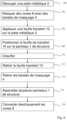
- FIG. 6 is a block diagram of the process flow, according to a particular arrangement.
- the structural panel 1 provided may be made of prepreg material (such as carbon fiber).
- the structural panel 1 can be made of composite material having fibrous layers (such as carbon fiber layers) which must be impregnated with a resin and polymerized to form the structural panel 1.
- the structural panel 1 provided may be in the process of being draped or already be polymerized.
- the method comprises a step of masking (step 202) of at least one predetermined zone 8 of the conductive metal track 2 with a masking strip 4 covering the, or each, zone 8.
- the masking tape 4 is a polyester tape adapted to withstand a polymerization temperature of the resin film 6.
- This masking step (step 202) is carried out before the application step (step 204) of the resin film 6 on the metal track 2.
- the application of a masking strip 4 (masking step 202) on predetermined zones 8 of the metal track 2 then makes it possible to obtain zones 8 devoid of the resin film 6, that is to say devoid of insulation.
- the resin film 6 is applied to the conductive metal track 2 having areas 8 masked with masking tape 4.
- the resin film 6 and the metal track 2 conductive having zones 8 masked with masking tape 4 are positioned on the structural panel 1.
- the resin film 6 makes it easier to manipulate the metal track 2.
- the resin film 6 makes it possible to easily manipulate the metal track 2 to position it on the structural panel 1.
- the resin film 6 can be applied (step 204) using a transfer sheet 10 (“wet peel ply” in English).
- transfer sheet 10 is meant a sheet of fabric or cellulose coated with the uncooked resin film 6.
- the use of a transfer sheet 10 is a particularly advantageous technical arrangement which makes it possible to facilitate the transport and handling of the resin film 6 and the metal track 2 glued to the resin film 6.
- the resin film 6 is applied without a transfer sheet 10.
- the resin film has a thickness between 30 ⁇ m and 150 ⁇ m.
- THE Figs. 1 and 2 represent the stack of layers of structural panel 1, metal track 2, masking strips 4 and transfer sheet 10 comprising the resin film 6, obtained after deposition of the transfer sheet 10 comprising the resin film 6.
- the metal track 2 is positioned on the structural panel 1.
- the masking strips 4 are positioned on the zones 8 of the metal track 2.
- the transfer sheet 10 comprising the resin film 6 covers the masking strips 4, the metal track 2 and the structural panel.
- the method then comprises a heating step (step 210) of the structural panel 1, of the conductive metal track 2 and of the transfer sheet 10 to heat-bond the resin film 6 to the conductive metal track 2 and the face of the structural panel 1.
- heating can be carried out in an oven.
- the objective of the heating step (step 210) is to heat-glue the resin film 6 so that it adheres to the structural panel 1 and to the metal track 2, covering them uniformly, which makes it possible to maintain the conductive metal track 2 against the structural panel 1.
- heating makes it possible to cook the panel 1 of composite material structure.
- the transfer sheet 10 is removed 212, leaving the resin film 6 heat-sealed (baked) on the structural panel 1, the metal track 2 and the masking strips 4.
- the heating step 210 makes it possible to polymerize the resin film 6 and the structural panel 1.
- the masking strips 4 are removed (step 214).
- the zones 8 of the conductive metal track 2 which were under the masking strips 4 are devoid of the resin film 6, which makes it possible to establish an electrical connection by contact on these zones 8.
- step 216 it is possible to assemble (step 216) several structural panels 1, then to connect (step 218) electrically by contact the zones 8 of these structural panels 1 to form an electrical circuit.
- step 218 electrically by contact the zones 8 of these structural panels 1 to form an electrical circuit.
Landscapes
- Engineering & Computer Science (AREA)
- Manufacturing & Machinery (AREA)
- Aviation & Aerospace Engineering (AREA)
- Microelectronics & Electronic Packaging (AREA)
- Transportation (AREA)
- Mechanical Engineering (AREA)
- Laminated Bodies (AREA)
Applications Claiming Priority (1)
| Application Number | Priority Date | Filing Date | Title |
|---|---|---|---|
| FR2210869 | 2022-10-20 |
Publications (1)
| Publication Number | Publication Date |
|---|---|
| EP4358657A1 true EP4358657A1 (de) | 2024-04-24 |
Family
ID=85222152
Family Applications (1)
| Application Number | Title | Priority Date | Filing Date |
|---|---|---|---|
| EP23204533.6A Pending EP4358657A1 (de) | 2022-10-20 | 2023-10-19 | Harzfolie |
Country Status (3)
| Country | Link |
|---|---|
| US (1) | US20240227360A9 (de) |
| EP (1) | EP4358657A1 (de) |
| CN (1) | CN118399151A (de) |
Citations (3)
| Publication number | Priority date | Publication date | Assignee | Title |
|---|---|---|---|---|
| US4506004A (en) * | 1982-04-01 | 1985-03-19 | Sullivan Donald F | Printed wiring board |
| WO1997038562A1 (fr) * | 1996-04-10 | 1997-10-16 | Matsushita Electric Industrial Co., Ltd. | Carte de montage de composants, procede de production de cette carte et procede de production du module |
| FR3002206A1 (fr) * | 2013-02-19 | 2014-08-22 | Airbus Operations Sas | Procede et dispositif pour afficher a l'aide d'au moins un film electronique une image dynamique sur un engin mobile, en particulier un aeronef. |
Family Cites Families (3)
| Publication number | Priority date | Publication date | Assignee | Title |
|---|---|---|---|---|
| TWI254995B (en) * | 2004-01-30 | 2006-05-11 | Phoenix Prec Technology Corp | Presolder structure formed on semiconductor package substrate and method for fabricating the same |
| KR102123475B1 (ko) * | 2012-12-05 | 2020-06-26 | 사이텍 인더스트리스 인코포레이티드 | 합성 구조물용 전도성 표면재 |
| EP3216690B1 (de) * | 2016-03-07 | 2018-11-07 | Airbus Operations GmbH | Verfahren zur herstellung eines verkleidungspaneels |
-
2023
- 2023-10-18 US US18/489,143 patent/US20240227360A9/en active Pending
- 2023-10-19 EP EP23204533.6A patent/EP4358657A1/de active Pending
- 2023-10-19 CN CN202311361360.XA patent/CN118399151A/zh active Pending
Patent Citations (3)
| Publication number | Priority date | Publication date | Assignee | Title |
|---|---|---|---|---|
| US4506004A (en) * | 1982-04-01 | 1985-03-19 | Sullivan Donald F | Printed wiring board |
| WO1997038562A1 (fr) * | 1996-04-10 | 1997-10-16 | Matsushita Electric Industrial Co., Ltd. | Carte de montage de composants, procede de production de cette carte et procede de production du module |
| FR3002206A1 (fr) * | 2013-02-19 | 2014-08-22 | Airbus Operations Sas | Procede et dispositif pour afficher a l'aide d'au moins un film electronique une image dynamique sur un engin mobile, en particulier un aeronef. |
Also Published As
| Publication number | Publication date |
|---|---|
| US20240131820A1 (en) | 2024-04-25 |
| US20240227360A9 (en) | 2024-07-11 |
| CN118399151A (zh) | 2024-07-26 |
Similar Documents
| Publication | Publication Date | Title |
|---|---|---|
| CA2727749C (fr) | Systeme de drainage d'un courant de foudre genere par une decharge orageuse sur un aeronef | |
| EP0188160B1 (de) | Enteisungsanlage für eine Flügelstruktur | |
| EP2557572B1 (de) | Teilentladungsbeständiges elektrisches kabel | |
| EP2321178B1 (de) | Fertigungsverfahren für eine enteisungsstruktur einer triebwerksgondel | |
| EP2143637B1 (de) | Verfahren zum Zusammenbau einer Enteisungsdecke und eines Metallbelags auf einer Struktur | |
| EP3461620B1 (de) | Verfahren zum widerstandsschweissen von faserverbundkomponenten zur verleihung einer faserverbundstruktur, faserverbundstruktur und faserverbundkomponente | |
| EP3241416B1 (de) | Struktur mit elektrisch leitenden oberflächenbahnen sowie verfahren zur herstellung von elektrisch leitenden bahnen auf einer oberfläche einer struktur | |
| EP0778588B1 (de) | Flachkabel mit kleiner Marge | |
| EP0397163A1 (de) | Dichte Umhüllung auf der Basis einer faserartigen Umwicklung und zusammengesetzter Blitzableiter als Anwendung | |
| EP0717585B1 (de) | Verbundmaterial und Verbundelement mit dadurch sichergestellter elektrischer Kontinuität, dessen Herstellungsverfahren und dessen Verwendung in Flugzeugindustrie | |
| EP1269604A1 (de) | Elektrischer verbinder mit mehrfachkontaktelementen und drehende elektrische maschine mit einem solchen verbinder | |
| EP4358657A1 (de) | Harzfolie | |
| EP2715742A1 (de) | Halberzeugnis in form eines leitenden streifens zur eingebettung in einem verbundwerkstoff und verfahren zur herstellung eines solchen streifens | |
| EP0619691B2 (de) | Glasscheibe mit Anschlusselement | |
| EP1605474B1 (de) | Kabel mit mehreren isolierten Leitern in einem Mantel und Herstellungsverfahren des Kabels. | |
| EP1260992B1 (de) | Verfahren zur Herstellung eines elektrischen Verbundisolators mit einer Aussenschicht und mindestens einer optischen Faser, die miteinander kompatibel sind | |
| FR3139149A1 (fr) | Procédé pour renforcer un ouvrage de construction et dispositif pour un tel procédé | |
| CA3193859A1 (fr) | Systeme et procede de solidarisation de pieces thermoplastiques hautes performances | |
| WO2023247851A1 (fr) | Harnais électrique de puissance pour aéronef | |
| FR3012913A1 (fr) | Dispositif de connexion electrique en parallele d'elements electrochimiques | |
| FR3104061A1 (fr) | Matériau parafoudre et procédé pour fabriquer un composant composite fibreux | |
| FR2685250A1 (fr) | Procede d'incorporation d'un element de rechauffage dans une structure en materiau composite. | |
| FR2952905A1 (fr) | Dispositif d'attache de moyens raidisseurs a un element de cadre, et structure comportant un tel dispositif d'attache | |
| FR2609204A1 (fr) | Cable electrique, notamment pour aeronef | |
| WO2013004774A1 (fr) | Structure assemblée à continuité électrique |
Legal Events
| Date | Code | Title | Description |
|---|---|---|---|
| PUAI | Public reference made under article 153(3) epc to a published international application that has entered the european phase |
Free format text: ORIGINAL CODE: 0009012 |
|
| STAA | Information on the status of an ep patent application or granted ep patent |
Free format text: STATUS: THE APPLICATION HAS BEEN PUBLISHED |
|
| AK | Designated contracting states |
Kind code of ref document: A1 Designated state(s): AL AT BE BG CH CY CZ DE DK EE ES FI FR GB GR HR HU IE IS IT LI LT LU LV MC ME MK MT NL NO PL PT RO RS SE SI SK SM TR |