EP4325563A2 - Semiconductor devices with a structure capable of suppressing coupling noise suppression - Google Patents
Semiconductor devices with a structure capable of suppressing coupling noise suppression Download PDFInfo
- Publication number
- EP4325563A2 EP4325563A2 EP23185275.7A EP23185275A EP4325563A2 EP 4325563 A2 EP4325563 A2 EP 4325563A2 EP 23185275 A EP23185275 A EP 23185275A EP 4325563 A2 EP4325563 A2 EP 4325563A2
- Authority
- EP
- European Patent Office
- Prior art keywords
- trace
- segment
- semiconductor device
- seg
- current signal
- Prior art date
- Legal status (The legal status is an assumption and is not a legal conclusion. Google has not performed a legal analysis and makes no representation as to the accuracy of the status listed.)
- Pending
Links
Images




Classifications
-
- H—ELECTRICITY
- H10—SEMICONDUCTOR DEVICES; ELECTRIC SOLID-STATE DEVICES NOT OTHERWISE PROVIDED FOR
- H10W—GENERIC PACKAGES, INTERCONNECTIONS, CONNECTORS OR OTHER CONSTRUCTIONAL DETAILS OF DEVICES COVERED BY CLASS H10
- H10W20/00—Interconnections in chips, wafers or substrates
- H10W20/40—Interconnections external to wafers or substrates, e.g. back-end-of-line [BEOL] metallisations or vias connecting to gate electrodes
- H10W20/41—Interconnections external to wafers or substrates, e.g. back-end-of-line [BEOL] metallisations or vias connecting to gate electrodes characterised by their conductive parts
- H10W20/423—Shielding layers
-
- H—ELECTRICITY
- H10—SEMICONDUCTOR DEVICES; ELECTRIC SOLID-STATE DEVICES NOT OTHERWISE PROVIDED FOR
- H10W—GENERIC PACKAGES, INTERCONNECTIONS, CONNECTORS OR OTHER CONSTRUCTIONAL DETAILS OF DEVICES COVERED BY CLASS H10
- H10W44/00—Electrical arrangements for controlling or matching impedance
- H10W44/501—Inductive arrangements
-
- H—ELECTRICITY
- H10—SEMICONDUCTOR DEVICES; ELECTRIC SOLID-STATE DEVICES NOT OTHERWISE PROVIDED FOR
- H10D—INORGANIC ELECTRIC SEMICONDUCTOR DEVICES
- H10D1/00—Resistors, capacitors or inductors
- H10D1/20—Inductors
-
- H—ELECTRICITY
- H10—SEMICONDUCTOR DEVICES; ELECTRIC SOLID-STATE DEVICES NOT OTHERWISE PROVIDED FOR
- H10W—GENERIC PACKAGES, INTERCONNECTIONS, CONNECTORS OR OTHER CONSTRUCTIONAL DETAILS OF DEVICES COVERED BY CLASS H10
- H10W20/00—Interconnections in chips, wafers or substrates
- H10W20/40—Interconnections external to wafers or substrates, e.g. back-end-of-line [BEOL] metallisations or vias connecting to gate electrodes
- H10W20/41—Interconnections external to wafers or substrates, e.g. back-end-of-line [BEOL] metallisations or vias connecting to gate electrodes characterised by their conductive parts
- H10W20/43—Layouts of interconnections
- H10W20/432—Layouts of interconnections comprising crossing interconnections
-
- H—ELECTRICITY
- H10—SEMICONDUCTOR DEVICES; ELECTRIC SOLID-STATE DEVICES NOT OTHERWISE PROVIDED FOR
- H10W—GENERIC PACKAGES, INTERCONNECTIONS, CONNECTORS OR OTHER CONSTRUCTIONAL DETAILS OF DEVICES COVERED BY CLASS H10
- H10W20/00—Interconnections in chips, wafers or substrates
- H10W20/40—Interconnections external to wafers or substrates, e.g. back-end-of-line [BEOL] metallisations or vias connecting to gate electrodes
- H10W20/497—Inductive arrangements or effects of, or between, wiring layers
Definitions
- On-chip inductor is a general element frequently used in semiconductor devices, but it is a very sensitive block which is easily interfered by coupling noises of other aggressors.
- the aggressors might be on-chip, package, or PCB circuits or layout routings. Moving the aggressor far away is a known solution, but it will make larger chip area, which leads to higher cost.
- a semiconductor device comprises an electronic device, a guard trace and a first trace.
- the guard trace is connecting to a ground layer through a first ground via.
- the first trace is disposed adjacent to the electronic device and the guard trace and comprises a first segment. A phase or a direction of a first current signal conducted on the first trace is changed in the first segment.
- the electronic device and the first trace are disposed at different sides of the guard trace and the first ground via is beside the first segment.
- a semiconductor device comprises an inductor, a guard trace and a differential circuit.
- the guard trace is connecting to a ground layer through a first ground via.
- the differential circuit is disposed adjacent to the inductor and the guard trace and comprises a first segment. A phase or a direction of a first current signal conducted in the differential circuit is changed in the first segment.
- the inductor and the differential circuit are disposed at different sides of the guard trace, the guard trace extends along a first direction, and the first ground via is arranged aside the first segment along a second direction substantially perpendicular to the first direction.
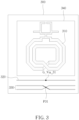
- FIG. 1 illustrates an exemplary top view of a semiconductor device according to an embodiment of the invention.
- the semiconductor device 100 may comprise an electronic device 110, a guard trace 120 and a differential circuit, such as a differential pair 130.
- the electronic device 110 may be an inductive device, such as an inductor, and the electronic device 110 may be one of the components forming a resonant cavity in the semiconductor device 100.
- the electronic device 110 may be an inductive device or an inductor which is capable of forming a resonant cavity with a capacitor.
- the electronic device 110 may be an inductor comprised in an Inductance Capacitance Voltage Controlled Oscillator (LC-VCO).
- LC-VCO Inductance Capacitance Voltage Controlled Oscillator
- FIG. 1 presents a simplified diagram of a semiconductor device in which only the components relevant to the invention are shown.
- a semiconductor device may further comprise other components not shown in FIG. 1 and configured for implementing the corresponding functions thereof, such as the aforementioned capacitor and/or the components other than an inductor comprised in an LC-VCO. Therefore, the components in a semiconductor device should not be limited to what is shown in FIG. 1 .
- the differential circuit such as the differential pair 130
- the differential pair 130 may be an aggressor device to the electronic device 110.
- the electronic device 110 may be greatly interfered by the coupling noise generated or induced by the differential pair 130.
- a phenomenon of such interference is a notorious problem named VCO phase noise.
- moving the aggressor device far away is a known solution, but it will make larger chip area, which leads to higher cost.
- the aggressor device instead of moving the aggressor device (such as the differential pair 130) far away from victim device (such as the electronic device 110), the aggressor device may be designed to have a twisted structure or may be designed to have a structure, or in some embodiments of the invention comprise a circuit or device, to change a phase or a direction of a current signal conducted thereon or conducted therein, so as to suppress the coupling noise caused by the aggressor device. More details will be discussed in the following paragraphs.
- the semiconductor device 100 may also comprise a surrounding metal 140.
- the surrounding metal 140 may have a closed loop structure and is arranged to surround the electronic device 110 to suppress coupling noise from any aggressor device adjacent to the electronic device 110. That is, in the corresponding preferred embodiments of the invention, the electronic device 110 is encompassed by the surrounding metal 140.
- a projection area of the surrounding metal 140 on a predetermined plane surrounds a projection area of the electronic device 110 on the predetermined plane, where the predetermined plane may be any layer of the semiconductor device 100 or may be a top surface (or plane) or bottom surface (or plane) of the semiconductor device 100.
- the guard trace 120 may be disposed between the electronic device 110 and the aggressor device, such as the differential circuit or the differential pair 130.
- the electronic device 110 and the aggressor device, such as the differential circuit or the differential pair 130 may be disposed at different sides of the guard trace 120.
- the guard trace 120 may be connected to a ground layer having a ground potential through a ground via G_Via_11.
- FIG. 2 is a drawing of partial enlargement of a top view of the aggressor device having a twisted structure to suppress the coupling noise induced thereby according to an embodiment of the invention.
- the aggressor device is a differential circuit, such as a pair 230, and may comprise traces T1 and T2.
- the traces T1 and T2 are disposed adjacent to the electronic device (e.g., the electronic device 110 shown in FIG. 1 ) and the guard trace (e.g., the guard trace 120 shown in FIG. 1 ).
- the traces T1 and T2 may be substantially arranged in parallel and may respectively comprise a plurality of portions or segments.
- the traces T1 and T2 may extend substantially in parallel along a first direction (e.g., a vertical direction from one end or terminal of the trace T1/T2 to another end or terminal of the trace T1/T2).
- the traces T1 and T2 may comprise un-twisted portions or segments, such as the upper portions or upper segments Seg_10 and Seg_20 and the lower portions or upper segments Seg_12 and Seg_22, and one or more twisted portions or segments, such as the portions or segments Seg_11 and Seg_21 which are located in the middle of the traces T1 and T2 and are visually overlapped. It is to be noted that although the middle portions or middle segments of the traces T1 and T2 are visually overlapped from the top view of the layout of the semiconductor device as shown in FIG. 2 , the traces T1 and T2 are actually physical separated and are electrically disconnected.
- the twisted portions or segments of a differential pair having a twisted structure is not limited to be located in the middle of the traces. Alternatively preferably, the twisted portions or segments of a differential pair having a twisted structure may be located in any position of the corresponding traces.
- the layout of the trace T1 and the layout of the trace T2 cross over one another with overlaid intersecting slanting portions or segments, which may also be referred as the twisted portions or segments, such as the segment Seg_11 of the trace T1 and the segment Seg_21 of the trace T2, thereby forming an "X" shaped cross as shown in FIG. 2 .
- a projection area of the segment Seg_11 on the predetermined plane and a projection area of the segment Seg_21 on the predetermined plane are overlapped at a twisting point, such as the twisting point P21 shown in FIG. 2 .
- the traces T1 and T2 are physical separated and are electrically disconnected. Therefore, one of the traces T1 and T2 may have a cross-layer structure.
- the segment Seg_21 filled with slashes may be implemented in a layer different from the trace T1 and the segments Seg_20 and Seg_22 of the trace T2.
- the relative distance of the current signal conducted on the trace T1 in the differential circuit to the guard trace and the electronic device and the relative distance of the current signal conducted on the trace T2 in the differential circuit to the guard trace and the electronic device are changed or switched during the travel in the respective trace.
- the guard trace and the electronic device are disposed at the right side of the differential pair 230
- the upper portion or upper segment Seg_20 is the one closer to the guard trace and the electronic device
- the lower portion or lower segment Seg_12 is the one closer to the guard trace and the electronic device.
- FIG. 2 also shows the flows of current signals conducted on the traces T1 and T2.
- the current signal I1 (as well as I1' and I1") is the current signal conducted on the trace T1 and the current signal I2 (as well as I2' and I2") is the current signal conducted on the trace T2.
- the current signal I1 and the current signal I1' are actually the same current signal with different flowing directions and/or phase.
- the current signal I1' and the current signal I1" are actually the same current signal with different flowing directions and/or phase.
- the current signal I1 and the current signal I1" are the same current signal with the same flowing direction (e.g., flowing upward in the vertical direction) but different relative distance to the guard trace and the electronic device.
- the current signal I2 and the current signal I2' are actually the same current signal with different flowing directions and/or phase.
- the current signal I2' and the current signal I2" are actually the same current signal with different flowing directions and/or phase.
- the current signal I2 and the current signal I2" are the same current signal with the same flowing direction (e.g., flowing downward in the vertical direction) but different relative distance to the guard trace and the electronic device.
- the phase and/or the direction of the current signal I1 (as well as I1' and I1") conducted on the trace T1 is changed in the segment Seg_11 (e.g. the current signal I1' with a phase and/or flowing direction different from that of the current signals I1 and 11") and the phase and/or the direction of the current signal I2 (as well as I2' and I2") conducted on the trace T2 is changed in the segment Seg_21 (e.g. the current signal I2' with a phase and/or flowing direction different from that of the current signals I2 and I2").
- the phase of the current signal changes as well. Therefore, in the corresponding preferred embodiments of the invention, for the portions or segments that are relatively closer to the guard trace and the electronic device, such as the upper portion or upper segment Seg_20 and the lower portion or lower segment Seg_12, since the current signals, such as the current signals I2 and I1, conducted thereon have different directions and/or phases, directions of the magnetic fields or magnetic lines induced by the current signals I1 and I2 are different. For example, the directions of the magnetic fields or magnetic lines induced by the current signals I1 and I2 are opposite. In this manner, the magnetic fields or magnetic lines induced by the current signals I1 and I2 may weaken or even cancel each other.
- the ground via G_Via_11 may be arranged beside the segments Seg_11 and Seg_21, and may be preferably arranged beside the twisting point, such as the twisting point P11 shown in FIG. 1 and/or the twisting point P21 shown in FIG. 2 .
- the ground via G_Via_11 may be arranged aside the segments Seg_11 and Seg_21 along a second direction (e.g., a horizontal direction) substantially perpendicular to the first direction.
- the ground via G_Via_11 may be arranged aside the twisting point P11/P21 along the second direction that is substantially perpendicular to the first direction.
- the ground via G_Via_11 may be located at a position on the guard trace 120 that is neighboring to the segments Seg_11 and Seg_21.
- the ground via G_Via_11 may be located at a position on the guard trace 120 that is closest to the twisting point, such as the twisting point P11 shown in FIG. 1 and/or the twisting point P21 shown in FIG. 2 .
- the position of the ground via G_Via_11 may also be flexibly adjusted.
- the position of the ground via G_Via_11 on the guard trace 120 may be chosen to a place to maximize the enhancement of coupling noise suppression, and is not limited to the position that is neighboring, aside, or closest to the segments Seg_11 and Seg_21 or the twisting point P11. Note further that since a semiconductor device may further comprise other components not shown in FIG.
- the position of the guard trace and the position of the ground via may be flexibly chosen to a place to maximize the enhancement of coupling noise suppression, as well as the distance between the guard trace and the aggressor device, the distance between the guard trace and the electronic device and the distance between the aggressor device and the electronic device may be flexibly adjusted based on the circuit design requirement. Therefore, the aforementioned positions and the aforementioned distances are certainly not the limit of the invention.
- guard trace 120 and the electronic device 110 are disposed at the right side of the aggressor device, such as the differential pair 130/230, the invention should not be limited thereto. In other embodiments of the invention, the guard trace and the aggressor device may be disposed in anywhere adjacent to the victim electronic device.
- FIG. 3 illustrates an exemplary top view of a semiconductor device according to another embodiment of the invention.
- the semiconductor device 300 may comprise an electronic device 310, a guard trace 320, a differential pair 330 and a surrounding metal 340.
- the guard trace 320 may be connected to a ground layer having a ground potential through the ground via G_Via_31 and the differential pair 330 may have a twisted structure with a twisting point P31.
- the guard trace 320 and the differential pair 330 are disposed at a different side of the electronic device as compared to the embodiment shown in FIG. 1 .
- FIG. 3 most of the elements shown in FIG. 3 are the same as in FIG. 1 , and the only difference may be in the positions of the guard trace 320 and the differential pair 330 relative to the electronic device 310. Since like reference numerals in FIG. 3 refer to like features in FIG. 1 , details with respect to like elements in FIG. 3 may refer to the descriptions regarding FIG. 1 and FIG. 2 , and will not be repeated herein.
- crossover and twisting points should not be a limit of the invention.
- FIG. 4 illustrates an exemplary top view of a semiconductor device according to yet another embodiment of the invention.
- the semiconductor device 400 may comprise an electronic device 410, a guard trace 420, a differential pair 430 and a surrounding metal 440.
- the differential pair 430 comprises traces T1' and T2' and has a twisted structure with three crossovers and three twisting points P41, P42 and P43.
- the guard trace 420 also comprises three ground vias G_Via_41, G_Via_42 and G_Via_43 and is connected to a ground layer having a ground potential through the ground vias.
- the phase or the direction of the current signal conducted on the trace T 1' is substantially the same in the corresponding un-twisted segments, and will be changed in the first twisted segment of the trace T1' corresponding to the twisting point P41, and then changed in the second twisted segment of the trace T1' corresponding to the twisting point P42, and further changed in the third twisted segment of the trace T1' corresponding to the twisting point P43 (when it is assumed that the current signal conducted on the trace T 1' flows downward).
- phase or the direction of the current signal conducted on the trace T2' is substantially the same in the corresponding un-twisted segments, and will be changed in the third twisted segment of the trace T2' corresponding to the twisting point P43, and then changed in the second twisted segment of the trace T2' corresponding to the twisting point P42, and further changed in the first twisted segment of the trace T2' corresponding to the twisting point P41 (when it is assumed that the current signal conducted on the trace T2' flows upward).
- the ground vias G_Via_41 may be located at a position on the guard trace 420 that is beside or neighboring to the first intersecting slanting segments (e.g., the first twisted segments corresponding to the twisting point P41).
- the ground via G_Via_41 may be located at a position on the guard trace 420 that is closest to the twisting point P41.
- the ground vias G_Via_42 may be located at a position on the guard trace 420 that is beside or neighboring to the second intersecting slanting segments (e.g., the second twisted segments corresponding to the twisting point P42).
- the ground via G_Via_42 may be located at a position on the guard trace 420 that is closest to the twisting point P42.
- the ground vias G_Via_43 may be located at a position on the guard trace 430 that is beside or closest to the third intersecting slanting segments (e.g., the third twisted segments corresponding to the twisting point P43).
- the ground via G_Via_43 may be located at a position on the guard trace 420 that is closest to the twisting point P43.
- FIG. 4 Since most of the elements shown in FIG. 4 are the same as in FIG. 1 , and the only difference may be in the number of ground vias and twisting points, like reference numerals in FIG. 4 refer to like features in FIG. 1 . Details with respect to like elements in FIG. 4 may refer to the descriptions regarding FIG. 1 and FIG. 2 , and will not be repeated herein.
- the aggressor device to the electronic device may also be a single-ended transmission line or trace (hereinafter the term "trace" is utilized to represent the description of "transmission line or trace” for brevity).
- the single-ended trace may comprise a circuit or device to change a phase or a direction of a current signal conducted thereon, so as to suppress the coupling noise caused by the single-ended trace.
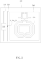
- FIG. 5 illustrates an exemplary top view of a semiconductor device according to yet another embodiment of the invention.
- the semiconductor device 500 may comprise an electronic device 510, a guard trace 520, a single-ended trace 530 and a surrounding metal 540.
- the guard trace 520 may be connected to a ground layer having a ground potential through the ground via G_Via_51 and the single-ended trace 530 may comprise an inverter circuit 533 configured thereon to change the direction or phase of the current signal conducted on the single-ended trace 530.
- the ground via G_Via_51 may be located at a position on the guard trace 520 that is beside or neighboring to the inverter circuit 533.
- the position of the single-ended trace 530 on where the inverter circuit 533 is located may also be regarded as a portion or a segment of the single-ended trace 530.
- the ground via G_Via_51 may be located at a position on the guard trace 520 that is beside or neighboring to the segment comprising the inverter circuit 533, and the phase or the direction of a current signal conducted on the single-ended trace 530 is changed in the aforementioned segment comprising the inverter circuit 533.
- the ground via G_Via_51 may be located at a position on the guard trace 520 that is closest to the point where the phase or the direction of the current signal conducted on the single-ended trace 530 is changed.
- the ground via G_Via_51 may be arranged aside the inverter circuit 533 or the segment comprising the inverter circuit 533 along a second direction (e.g., a horizontal direction in FIG. 5 ) substantially perpendicular to the first direction (e.g., a vertical direction in FIG. 5 ) in which the guard trace 520 and the single-ended trace 530 extend.
- a second direction e.g., a horizontal direction in FIG. 5
- the first direction e.g., a vertical direction in FIG. 5
- the position of the ground via G_Via_51 may also be flexibly adjusted. Since the guard trace and the ground via are utilized to further enhance the suppression of the coupling noise, the position of the ground via G_Via_51 may be chosen to a place to maximize the enhancement of coupling noise suppression. In addition, since a semiconductor device may further comprise other components not shown in FIG.
- the position of the guard trace and the position of the ground via may be flexibly chosen to a place to maximize the enhancement of coupling noise suppression, as well as the distance between the guard trace and the aggressor device, such as the single-ended trace, the distance between the guard trace and the electronic device and the distance between the aggressor device and the electronic device may be flexibly adjusted based on the circuit design requirement. Therefore, the aforementioned positions and the aforementioned distances are certainly not the limit of the invention.
- FIG. 5 It is to be noted that most of the elements shown in FIG. 5 are the same as in FIG. 1 , and the only difference may be in the type of the aggressor device to the electronic device 510. Since like reference numerals in FIG. 5 refer to like features in FIG. 1 , details with respect to like elements may refer to the descriptions regarding FIG. 1 and FIG. 2 , and will not be repeated herein. It is to be further noted that a person of ordinary skill in the art will be readily appreciated to deduce the changes in the flowing direction of the current signal conducted on the single-ended trace comprising one or more inverter circuits based on the illustration regarding FIG. 2 and the description above, therefore, details regarding the direction of current flow on the single-ended trace with one or more inverter circuits are omitted here for brevity.
- the magnetic fields or magnetic lines induced by the current signal when the current signal is flowing through different segments may weaken or even cancel each other. In this manner, the induced coupling noise is effectively suppressed.
- inverter circuit there is one inverter circuit in the embodiment shown in FIG. 5 , a specific number of inverter circuit should not be a limit of the invention. In other embodiments of the invention, there may be more than one inverter circuit comprised in the single-ended trace.
- FIG. 6 illustrates an exemplary top view of a semiconductor device according to yet another embodiment of the invention.
- the semiconductor device 600 may comprise an electronic device 610, a guard trace 620, a single-ended trace 630 and a surrounding metal 640.
- the single-ended trace 630 comprises two inverter circuits 633 and 635.
- the guard trace 620 also comprises two ground vias G_Via_61 and G_Via_62 and is connected to a ground layer having a ground potential through the ground vias.
- the inverter circuits 633 and 635 are both configured on the single-ended trace 630 to change the direction or phase of the current signal conducted on the single-ended trace 630.
- the ground via G_Via_61 may be located at a position on the guard trace 620 that is beside or neighboring to the inverter circuit 633, and the ground via G_Via_62 may be located at a position on the guard trace 620 that is beside or neighboring to the inverter circuit 635.
- the position of the single-ended trace 630 on where an inverter circuit is located may also be regarded as a portion or a segment of the single-ended trace 630.
- the ground via G_Via_61 may be located at a position on the guard trace 620 that is beside or neighboring to the segment comprising the inverter circuit 633 and the phase or the direction of a current signal conducted on the single-ended trace 630 is changed in the segment comprising the inverter circuit 633
- the ground via G_Via_62 may be located at a position on the guard trace 620 that is beside or neighboring to the segment comprising the inverter circuit 635 and the phase or the direction of the current signal conducted on the single-ended trace 630 is further changed in the segment comprising the inverter circuit 635.
- the ground via G_Via_61 may be located at a position on the guard trace 620 that is closest to the point where the phase or the direction of the current signal conducted on the single-ended trace 630 is changed, and the ground via G_Via_62 may be located at a position on the guard trace 620 that is closest to the point where the phase or the direction of the current signal conducted on the single-ended trace 630 is further changed.
- the ground via G_Via_61 may be arranged aside the inverter circuit 633 or the segment comprising the inverter circuit 633 along a second direction (e.g., a horizontal direction in FIG. 6 ) substantially perpendicular to the first direction (e.g., a vertical direction in FIG. 6 ) in which the guard trace 620 and the single-ended trace 630 extend, and the ground via G_Via_62 may also be arranged aside the inverter circuit 635 or the segment comprising the inverter circuit 635 along the second direction.
- a second direction e.g., a horizontal direction in FIG. 6
- the ground via G_Via_62 may also be arranged aside the inverter circuit 635 or the segment comprising the inverter circuit 635 along the second direction.
- the electronic device comprised in the semiconductor device and being interfered by the aggressor device may be any shape of inductive device and/or inductor that is suitable to provide an inductance. Therefore, although the spiral-shape inductors are shown in the drawings for illustration, the spiral-shape should not be a limit of the invention.
- the magnetic fields or magnetic lines induced by the current signal when it is flowing in different segments may weaken or even cancel each other.
- Such phenomenon of being weakened or even cancelled will be generated in both the traces of a differential pair having the twisted structure and a single-ended trace. In this manner, the induced coupling noise is effectively suppressed.
Landscapes
- Semiconductor Integrated Circuits (AREA)
- Internal Circuitry In Semiconductor Integrated Circuit Devices (AREA)
- Engineering & Computer Science (AREA)
- Power Engineering (AREA)
Abstract
Description
- This application claims the benefit of
U.S. Provisional Application No. 63/369,394, filed on July 26th, 2022 - On-chip inductor is a general element frequently used in semiconductor devices, but it is a very sensitive block which is easily interfered by coupling noises of other aggressors. The aggressors might be on-chip, package, or PCB circuits or layout routings. Moving the aggressor far away is a known solution, but it will make larger chip area, which leads to higher cost.
- Therefore, a new solution deploying to the semiconductor device structure being effective for the suppression of the coupling noise is highly required.
- Semiconductor devices according to the invention are defined in the independent claims. The dependent claims define preferred embodiments thereof. According to an embodiment of the invention, a semiconductor device comprises an electronic device, a guard trace and a first trace. The guard trace is connecting to a ground layer through a first ground via. The first trace is disposed adjacent to the electronic device and the guard trace and comprises a first segment. A phase or a direction of a first current signal conducted on the first trace is changed in the first segment. The electronic device and the first trace are disposed at different sides of the guard trace and the first ground via is beside the first segment.
- According to another embodiment of the invention, a semiconductor device comprises an inductor, a guard trace and a differential circuit. The guard trace is connecting to a ground layer through a first ground via. The differential circuit is disposed adjacent to the inductor and the guard trace and comprises a first segment. A phase or a direction of a first current signal conducted in the differential circuit is changed in the first segment. The inductor and the differential circuit are disposed at different sides of the guard trace, the guard trace extends along a first direction, and the first ground via is arranged aside the first segment along a second direction substantially perpendicular to the first direction.
- These and other objectives of the present invention will no doubt become obvious to those of ordinary skill in the art after reading the following detailed description of the preferred embodiment that is illustrated in the various figures and drawings.
-
-
FIG. 1 illustrates an exemplary top view of a semiconductor device according to an embodiment of the invention. -
FIG. 2 is a drawing of partial enlargement of a top view of the aggressor device having a twisted structure to suppress the coupling noise induced thereby according to an embodiment of the invention. -
FIG. 3 illustrates an exemplary top view of a semiconductor device according to another embodiment of the invention. -
FIG. 4 illustrates an exemplary top view of a semiconductor device according to yet another embodiment of the invention. -
FIG. 5 illustrates an exemplary top view of a semiconductor device according to yet another embodiment of the invention. -
FIG. 6 illustrates an exemplary top view of a semiconductor device according to yet another embodiment of the invention. -
FIG. 1 illustrates an exemplary top view of a semiconductor device according to an embodiment of the invention. Thesemiconductor device 100 may comprise anelectronic device 110, aguard trace 120 and a differential circuit, such as adifferential pair 130. In the embodiments of the invention, theelectronic device 110 may be an inductive device, such as an inductor, and theelectronic device 110 may be one of the components forming a resonant cavity in thesemiconductor device 100. As an example, theelectronic device 110 may be an inductive device or an inductor which is capable of forming a resonant cavity with a capacitor. In one embodiment of the invention, theelectronic device 110 may be an inductor comprised in an Inductance Capacitance Voltage Controlled Oscillator (LC-VCO). - It is to be noted
FIG. 1 presents a simplified diagram of a semiconductor device in which only the components relevant to the invention are shown. As will be readily appreciated by a person of ordinary skill in the art, a semiconductor device may further comprise other components not shown inFIG. 1 and configured for implementing the corresponding functions thereof, such as the aforementioned capacitor and/or the components other than an inductor comprised in an LC-VCO. Therefore, the components in a semiconductor device should not be limited to what is shown inFIG. 1 . - According to an embodiment of the invention, the differential circuit, such as the
differential pair 130, may be an aggressor device to theelectronic device 110. As an example, when thedifferential pair 130 is configured to conduct or transmit high-speed signals, such as (but not limited to) clock signals, theelectronic device 110 may be greatly interfered by the coupling noise generated or induced by thedifferential pair 130. A phenomenon of such interference is a notorious problem named VCO phase noise. As mentioned above, moving the aggressor device far away is a known solution, but it will make larger chip area, which leads to higher cost. - In the embodiments of the invention, instead of moving the aggressor device (such as the differential pair 130) far away from victim device (such as the electronic device 110), the aggressor device may be designed to have a twisted structure or may be designed to have a structure, or in some embodiments of the invention comprise a circuit or device, to change a phase or a direction of a current signal conducted thereon or conducted therein, so as to suppress the coupling noise caused by the aggressor device. More details will be discussed in the following paragraphs.
- In addition, to further suppress the coupling noise generated or induced by the aggressor device, the
semiconductor device 100 may also comprise a surroundingmetal 140. In the embodiments of the invention, the surroundingmetal 140 may have a closed loop structure and is arranged to surround theelectronic device 110 to suppress coupling noise from any aggressor device adjacent to theelectronic device 110. That is, in the corresponding preferred embodiments of the invention, theelectronic device 110 is encompassed by the surroundingmetal 140. Preferably, a projection area of the surroundingmetal 140 on a predetermined plane surrounds a projection area of theelectronic device 110 on the predetermined plane, where the predetermined plane may be any layer of thesemiconductor device 100 or may be a top surface (or plane) or bottom surface (or plane) of thesemiconductor device 100. - Preferably, the
guard trace 120 may be disposed between theelectronic device 110 and the aggressor device, such as the differential circuit or thedifferential pair 130. Preferably, theelectronic device 110 and the aggressor device, such as the differential circuit or thedifferential pair 130, may be disposed at different sides of theguard trace 120. Theguard trace 120 may be connected to a ground layer having a ground potential through a ground via G_Via_11. -
FIG. 2 is a drawing of partial enlargement of a top view of the aggressor device having a twisted structure to suppress the coupling noise induced thereby according to an embodiment of the invention. In this embodiment, the aggressor device is a differential circuit, such as apair 230, and may comprise traces T1 and T2. - Preferably, the traces T1 and T2 are disposed adjacent to the electronic device (e.g., the
electronic device 110 shown inFIG. 1 ) and the guard trace (e.g., theguard trace 120 shown inFIG. 1 ). The traces T1 and T2 may be substantially arranged in parallel and may respectively comprise a plurality of portions or segments. As an example, the traces T1 and T2 may extend substantially in parallel along a first direction (e.g., a vertical direction from one end or terminal of the trace T1/T2 to another end or terminal of the trace T1/T2). The traces T1 and T2 may comprise un-twisted portions or segments, such as the upper portions or upper segments Seg_10 and Seg_20 and the lower portions or upper segments Seg_12 and Seg_22, and one or more twisted portions or segments, such as the portions or segments Seg_11 and Seg_21 which are located in the middle of the traces T1 and T2 and are visually overlapped. It is to be noted that although the middle portions or middle segments of the traces T1 and T2 are visually overlapped from the top view of the layout of the semiconductor device as shown inFIG. 2 , the traces T1 and T2 are actually physical separated and are electrically disconnected. It is to be also noted that, the twisted portions or segments of a differential pair having a twisted structure is not limited to be located in the middle of the traces. Alternatively preferably, the twisted portions or segments of a differential pair having a twisted structure may be located in any position of the corresponding traces. - Preferably, the layout of the trace T1 and the layout of the trace T2 cross over one another with overlaid intersecting slanting portions or segments, which may also be referred as the twisted portions or segments, such as the segment Seg_11 of the trace T1 and the segment Seg_21 of the trace T2, thereby forming an "X" shaped cross as shown in
FIG. 2 . In the corresponding preferred embodiments of the invention, a projection area of the segment Seg_11 on the predetermined plane and a projection area of the segment Seg_21 on the predetermined plane are overlapped at a twisting point, such as the twisting point P21 shown inFIG. 2 . As noted above, in actual implementation, the traces T1 and T2 are physical separated and are electrically disconnected. Therefore, one of the traces T1 and T2 may have a cross-layer structure. As an example, the segment Seg_21 filled with slashes may be implemented in a layer different from the trace T1 and the segments Seg_20 and Seg_22 of the trace T2. - In the corresponding preferred embodiments of the invention, due to the twisted structure, the relative distance of the current signal conducted on the trace T1 in the differential circuit to the guard trace and the electronic device and the relative distance of the current signal conducted on the trace T2 in the differential circuit to the guard trace and the electronic device are changed or switched during the travel in the respective trace.
- To be more specific, assuming that the guard trace and the electronic device are disposed at the right side of the
differential pair 230, for the portions or segments above the twisting point P21, the upper portion or upper segment Seg_20 is the one closer to the guard trace and the electronic device, while for the portions or segments below the twisting point P21, the lower portion or lower segment Seg_12 is the one closer to the guard trace and the electronic device. -
FIG. 2 also shows the flows of current signals conducted on the traces T1 and T2. The current signal I1 (as well as I1' and I1") is the current signal conducted on the trace T1 and the current signal I2 (as well as I2' and I2") is the current signal conducted on the trace T2. The current signal I1 and the current signal I1' are actually the same current signal with different flowing directions and/or phase. The current signal I1' and the current signal I1" are actually the same current signal with different flowing directions and/or phase. The current signal I1 and the current signal I1" are the same current signal with the same flowing direction (e.g., flowing upward in the vertical direction) but different relative distance to the guard trace and the electronic device. Similarly, the current signal I2 and the current signal I2' are actually the same current signal with different flowing directions and/or phase. The current signal I2' and the current signal I2" are actually the same current signal with different flowing directions and/or phase. The current signal I2 and the current signal I2" are the same current signal with the same flowing direction (e.g., flowing downward in the vertical direction) but different relative distance to the guard trace and the electronic device. - Therefore, in the corresponding preferred embodiments of the invention, the phase and/or the direction of the current signal I1 (as well as I1' and I1") conducted on the trace T1 is changed in the segment Seg_11 (e.g. the current signal I1' with a phase and/or flowing direction different from that of the current signals I1 and 11") and the phase and/or the direction of the current signal I2 (as well as I2' and I2") conducted on the trace T2 is changed in the segment Seg_21 (e.g. the current signal I2' with a phase and/or flowing direction different from that of the current signals I2 and I2").
- Once the direction of a current signal changes, the phase of the current signal changes as well. Therefore, in the corresponding preferred embodiments of the invention, for the portions or segments that are relatively closer to the guard trace and the electronic device, such as the upper portion or upper segment Seg_20 and the lower portion or lower segment Seg_12, since the current signals, such as the current signals I2 and I1, conducted thereon have different directions and/or phases, directions of the magnetic fields or magnetic lines induced by the current signals I1 and I2 are different. For example, the directions of the magnetic fields or magnetic lines induced by the current signals I1 and I2 are opposite. In this manner, the magnetic fields or magnetic lines induced by the current signals I1 and I2 may weaken or even cancel each other. Similar phenomenon of being weakened or even cancelled may also occur to the magnetic fields or magnetic lines induced by the current signals I1" and I2" conducted on the traces having the twisted structure. In this manner, the induced coupling noise is effectively suppressed. Note that hereinafter the terms "segment" and "segments" are utilized to respectively represent the description of "portion or segment" and "portions or segments" for brevity.
- Referring to both
FIG. 1 andFIG. 2 , preferably, the ground via G_Via_11 may be arranged beside the segments Seg_11 and Seg_21, and may be preferably arranged beside the twisting point, such as the twisting point P11 shown inFIG. 1 and/or the twisting point P21 shown inFIG. 2 . Preferably, as theguard trace 120 and the traces T1 and T2 extend along a first direction (e.g., a vertical direction from one end or terminal of the trace T1/T2 to another end or terminal of the trace T1/T2), the ground via G_Via_11 may be arranged aside the segments Seg_11 and Seg_21 along a second direction (e.g., a horizontal direction) substantially perpendicular to the first direction. Preferably, the ground via G_Via_11 may be arranged aside the twisting point P11/P21 along the second direction that is substantially perpendicular to the first direction. - In a preferred embodiment of the invention, the ground via G_Via_11 may be located at a position on the
guard trace 120 that is neighboring to the segments Seg_11 and Seg_21. Preferably, in another or the same preferred embodiment of the invention, the ground via G_Via_11 may be located at a position on theguard trace 120 that is closest to the twisting point, such as the twisting point P11 shown inFIG. 1 and/or the twisting point P21 shown inFIG. 2 . Note that in other preferred embodiments of the invention, the position of the ground via G_Via_11 may also be flexibly adjusted. Since the guard trace and the ground via G_Via_11 are utilized to further enhance the suppression of the coupling noise, the position of the ground via G_Via_11 on theguard trace 120 may be chosen to a place to maximize the enhancement of coupling noise suppression, and is not limited to the position that is neighboring, aside, or closest to the segments Seg_11 and Seg_21 or the twisting point P11. Note further that since a semiconductor device may further comprise other components not shown inFIG. 1 for implementing the corresponding functions, the position of the guard trace and the position of the ground via may be flexibly chosen to a place to maximize the enhancement of coupling noise suppression, as well as the distance between the guard trace and the aggressor device, the distance between the guard trace and the electronic device and the distance between the aggressor device and the electronic device may be flexibly adjusted based on the circuit design requirement. Therefore, the aforementioned positions and the aforementioned distances are certainly not the limit of the invention. - It is also to be noted that although in the embodiment shown in
FIG. 1 , theguard trace 120 and theelectronic device 110 are disposed at the right side of the aggressor device, such as thedifferential pair 130/230, the invention should not be limited thereto. In other embodiments of the invention, the guard trace and the aggressor device may be disposed in anywhere adjacent to the victim electronic device. -
FIG. 3 illustrates an exemplary top view of a semiconductor device according to another embodiment of the invention. Thesemiconductor device 300 may comprise anelectronic device 310, aguard trace 320, adifferential pair 330 and a surroundingmetal 340. Theguard trace 320 may be connected to a ground layer having a ground potential through the ground via G_Via_31 and thedifferential pair 330 may have a twisted structure with a twisting point P31. In this embodiment, theguard trace 320 and thedifferential pair 330 are disposed at a different side of the electronic device as compared to the embodiment shown inFIG. 1 . - It is to be noted that most of the elements shown in
FIG. 3 are the same as inFIG. 1 , and the only difference may be in the positions of theguard trace 320 and thedifferential pair 330 relative to theelectronic device 310. Since like reference numerals inFIG. 3 refer to like features inFIG. 1 , details with respect to like elements inFIG. 3 may refer to the descriptions regardingFIG. 1 andFIG. 2 , and will not be repeated herein. - It is also to be noted that although there is one crossover as well as one twisting point in the embodiments shown in
FIG. 1 ,FIG. 2 andFIG.3 , a specific number of crossover and twisting points should not be a limit of the invention. In other embodiments of the invention, there may be more than one crossover and more than one twisting point comprised in the twisted structure, and therefore, there may be more than two un-twisted portions or segments comprised in each trace and more than one twisted portion or segment comprised in the corresponding trace. -
FIG. 4 illustrates an exemplary top view of a semiconductor device according to yet another embodiment of the invention. Thesemiconductor device 400 may comprise anelectronic device 410, aguard trace 420, adifferential pair 430 and a surroundingmetal 440. In this embodiment, thedifferential pair 430 comprises traces T1' and T2' and has a twisted structure with three crossovers and three twisting points P41, P42 and P43. To further enhance the suppression of the coupling noise, theguard trace 420 also comprises three ground vias G_Via_41, G_Via_42 and G_Via_43 and is connected to a ground layer having a ground potential through the ground vias. - In this embodiment, the phase or the direction of the current signal conducted on the trace T 1' is substantially the same in the corresponding un-twisted segments, and will be changed in the first twisted segment of the trace T1' corresponding to the twisting point P41, and then changed in the second twisted segment of the trace T1' corresponding to the twisting point P42, and further changed in the third twisted segment of the trace T1' corresponding to the twisting point P43 (when it is assumed that the current signal conducted on the trace T 1' flows downward). Likewise, the phase or the direction of the current signal conducted on the trace T2' is substantially the same in the corresponding un-twisted segments, and will be changed in the third twisted segment of the trace T2' corresponding to the twisting point P43, and then changed in the second twisted segment of the trace T2' corresponding to the twisting point P42, and further changed in the first twisted segment of the trace T2' corresponding to the twisting point P41 (when it is assumed that the current signal conducted on the trace T2' flows upward).
- According to a preferred embodiment of the invention, the ground vias G_Via_41 may be located at a position on the
guard trace 420 that is beside or neighboring to the first intersecting slanting segments (e.g., the first twisted segments corresponding to the twisting point P41). Preferably, in another or the same preferred embodiment of the invention, the ground via G_Via_41 may be located at a position on theguard trace 420 that is closest to the twisting point P41. Similarly, the ground vias G_Via_42 may be located at a position on theguard trace 420 that is beside or neighboring to the second intersecting slanting segments (e.g., the second twisted segments corresponding to the twisting point P42). Preferably, in an embodiment of the invention, the ground via G_Via_42 may be located at a position on theguard trace 420 that is closest to the twisting point P42. Likewise, the ground vias G_Via_43 may be located at a position on theguard trace 430 that is beside or closest to the third intersecting slanting segments (e.g., the third twisted segments corresponding to the twisting point P43). Preferably, in an embodiment of the invention, the ground via G_Via_43 may be located at a position on theguard trace 420 that is closest to the twisting point P43. - Since most of the elements shown in
FIG. 4 are the same as inFIG. 1 , and the only difference may be in the number of ground vias and twisting points, like reference numerals inFIG. 4 refer to like features inFIG. 1 . Details with respect to like elements inFIG. 4 may refer to the descriptions regardingFIG. 1 andFIG. 2 , and will not be repeated herein. - It is to be noted that although the differential pairs are provided in the abovementioned embodiments as the aggressor device, the invention should not be limited thereto. In other embodiments of the invention, the aggressor device to the electronic device may also be a single-ended transmission line or trace (hereinafter the term "trace" is utilized to represent the description of "transmission line or trace" for brevity). In the applications where the aggressor device is a single-ended trace, the single-ended trace may comprise a circuit or device to change a phase or a direction of a current signal conducted thereon, so as to suppress the coupling noise caused by the single-ended trace.
-
FIG. 5 illustrates an exemplary top view of a semiconductor device according to yet another embodiment of the invention. Thesemiconductor device 500 may comprise anelectronic device 510, aguard trace 520, a single-endedtrace 530 and a surroundingmetal 540. Theguard trace 520 may be connected to a ground layer having a ground potential through the ground via G_Via_51 and the single-endedtrace 530 may comprise aninverter circuit 533 configured thereon to change the direction or phase of the current signal conducted on the single-endedtrace 530. - In the corresponding preferred embodiments of the invention, there may be a phase difference around 180 degree in the current signal between two sides of the
inverter circuit 533, as an example, a phase difference around 180 degree at an operation frequency of the semiconductor device, where the phase is related to the operation frequency of thesemiconductor device 500. In addition, in the corresponding preferred embodiments of the invention, the ground via G_Via_51 may be located at a position on theguard trace 520 that is beside or neighboring to theinverter circuit 533. Note that the position of the single-endedtrace 530 on where theinverter circuit 533 is located may also be regarded as a portion or a segment of the single-endedtrace 530. Therefore, in the corresponding preferred embodiments of the invention, the ground via G_Via_51 may be located at a position on theguard trace 520 that is beside or neighboring to the segment comprising theinverter circuit 533, and the phase or the direction of a current signal conducted on the single-endedtrace 530 is changed in the aforementioned segment comprising theinverter circuit 533. Preferably, in a preferred embodiment of the invention, the ground via G_Via_51 may be located at a position on theguard trace 520 that is closest to the point where the phase or the direction of the current signal conducted on the single-endedtrace 530 is changed. In another or the same preferred embodiment of the invention, the ground via G_Via_51 may be arranged aside theinverter circuit 533 or the segment comprising theinverter circuit 533 along a second direction (e.g., a horizontal direction inFIG. 5 ) substantially perpendicular to the first direction (e.g., a vertical direction inFIG. 5 ) in which theguard trace 520 and the single-endedtrace 530 extend. - Note that in other preferred embodiments of the invention, the position of the ground via G_Via_51 may also be flexibly adjusted. Since the guard trace and the ground via are utilized to further enhance the suppression of the coupling noise, the position of the ground via G_Via_51 may be chosen to a place to maximize the enhancement of coupling noise suppression. In addition, since a semiconductor device may further comprise other components not shown in
FIG. 5 for implementing the corresponding functions, the position of the guard trace and the position of the ground via may be flexibly chosen to a place to maximize the enhancement of coupling noise suppression, as well as the distance between the guard trace and the aggressor device, such as the single-ended trace, the distance between the guard trace and the electronic device and the distance between the aggressor device and the electronic device may be flexibly adjusted based on the circuit design requirement. Therefore, the aforementioned positions and the aforementioned distances are certainly not the limit of the invention. - It is to be noted that most of the elements shown in
FIG. 5 are the same as inFIG. 1 , and the only difference may be in the type of the aggressor device to theelectronic device 510. Since like reference numerals inFIG. 5 refer to like features inFIG. 1 , details with respect to like elements may refer to the descriptions regardingFIG. 1 andFIG. 2 , and will not be repeated herein. It is to be further noted that a person of ordinary skill in the art will be readily appreciated to deduce the changes in the flowing direction of the current signal conducted on the single-ended trace comprising one or more inverter circuits based on the illustration regardingFIG. 2 and the description above, therefore, details regarding the direction of current flow on the single-ended trace with one or more inverter circuits are omitted here for brevity. - In the corresponding preferred embodiments of the invention, by changing the direction or phase of a current signal conducted on the single-ended trace during the travel in the single-ended trace, the magnetic fields or magnetic lines induced by the current signal when the current signal is flowing through different segments (such as the segment located above the inverter circuit and the segment located below the inverter circuit) may weaken or even cancel each other. In this manner, the induced coupling noise is effectively suppressed.
- It is to be noted that although there is one inverter circuit in the embodiment shown in
FIG. 5 , a specific number of inverter circuit should not be a limit of the invention. In other embodiments of the invention, there may be more than one inverter circuit comprised in the single-ended trace. -
FIG. 6 illustrates an exemplary top view of a semiconductor device according to yet another embodiment of the invention. Thesemiconductor device 600 may comprise anelectronic device 610, aguard trace 620, a single-endedtrace 630 and a surroundingmetal 640. In this embodiment, the single-endedtrace 630 comprises twoinverter circuits guard trace 620 also comprises two ground vias G_Via_61 and G_Via_62 and is connected to a ground layer having a ground potential through the ground vias. - The
inverter circuits trace 630 to change the direction or phase of the current signal conducted on the single-endedtrace 630. In the corresponding preferred embodiments of the invention, there may be a phase difference around 180 degree in the current signal between two sides of theinverter circuit 633, and a phase difference around 180 degree in the current signal between two sides of theinverter circuit 635. As an example, a phase difference around 180 degree at an operation frequency of thesemiconductor device 600, where the phase is related to the operation frequency of thesemiconductor device 600. In addition, in the corresponding preferred embodiments of the invention, the ground via G_Via_61 may be located at a position on theguard trace 620 that is beside or neighboring to theinverter circuit 633, and the ground via G_Via_62 may be located at a position on theguard trace 620 that is beside or neighboring to theinverter circuit 635. Note that the position of the single-endedtrace 630 on where an inverter circuit is located may also be regarded as a portion or a segment of the single-endedtrace 630. Therefore, in the corresponding preferred embodiments of the invention, the ground via G_Via_61 may be located at a position on theguard trace 620 that is beside or neighboring to the segment comprising theinverter circuit 633 and the phase or the direction of a current signal conducted on the single-endedtrace 630 is changed in the segment comprising theinverter circuit 633, and the ground via G_Via_62 may be located at a position on theguard trace 620 that is beside or neighboring to the segment comprising theinverter circuit 635 and the phase or the direction of the current signal conducted on the single-endedtrace 630 is further changed in the segment comprising theinverter circuit 635. Preferably, in a preferred embodiment of the invention, the ground via G_Via_61 may be located at a position on theguard trace 620 that is closest to the point where the phase or the direction of the current signal conducted on the single-endedtrace 630 is changed, and the ground via G_Via_62 may be located at a position on theguard trace 620 that is closest to the point where the phase or the direction of the current signal conducted on the single-endedtrace 630 is further changed. - In a corresponding preferred embodiment of the invention, the ground via G_Via_61 may be arranged aside the
inverter circuit 633 or the segment comprising theinverter circuit 633 along a second direction (e.g., a horizontal direction inFIG. 6 ) substantially perpendicular to the first direction (e.g., a vertical direction inFIG. 6 ) in which theguard trace 620 and the single-endedtrace 630 extend, and the ground via G_Via_62 may also be arranged aside theinverter circuit 635 or the segment comprising theinverter circuit 635 along the second direction. - In the embodiments of the invention, the electronic device comprised in the semiconductor device and being interfered by the aggressor device (such as a differential pair or a single-ended trace) may be any shape of inductive device and/or inductor that is suitable to provide an inductance. Therefore, although the spiral-shape inductors are shown in the drawings for illustration, the spiral-shape should not be a limit of the invention.
- In the embodiments of the invention, by changing the direction or phase of a current signal conducted on the trace during the travel in the trace, the magnetic fields or magnetic lines induced by the current signal when it is flowing in different segments may weaken or even cancel each other. Such phenomenon of being weakened or even cancelled will be generated in both the traces of a differential pair having the twisted structure and a single-ended trace. In this manner, the induced coupling noise is effectively suppressed.
- Those skilled in the art will readily observe that numerous modifications and alterations of the device and method may be made while retaining the teachings of the invention. Accordingly, the above disclosure should be construed as limited only by the metes and bounds of the appended claims.
Claims (15)
- A semiconductor device (100; 300; 400; 500; 600), comprising:an electronic component (110; 310; 410; 510; 610);a guard trace (120; 320; 420; 520; 620), connecting to a ground layer through a first ground via (G_Via_11; G_Via_31 G;_Via_41; G_ Via_51; G_Via_61); anda first trace (T1; T1'; 530; 630), disposed adjacent to the electronic component (110; 310; 410; 510; 610) and the guard trace (120; 320; 420; 520; 620) and comprising a first segment (Seg_11; 533; 633), wherein a phase or a direction of a first current signal conducted on the first trace (T1; T1'; 530; 630) is changed in the first segment (Seg_11; 533; 633), andwherein the electronic component (110; 310; 410; 510; 610) and the first trace (T1; T1'; 530; 630) are disposed at different sides of the guard trace (120; 320; 420; 520; 620) and the first ground via (G_Via_11; G_Via_31 G;_Via_41; G_Via_51; G_Via_61) is beside the first segment (Seg_11; 533; 633).
- The semiconductor device (100; 300; 400; 500; 600) of claim 1, whereinthe electronic component (110; 310; 410; 510; 610) is an electronic device, in particular an inductive device, or an inductor; and/orthe first trance (T1; T1'; 530; 630) is or represents a differential circuit that is disposed adjacent to the electronic component (110; 310; 410; 510; 610) and the guard trace (120; 320; 420; 520; 620) and comprises the first segment (Seg_11; 533; 633), wherein a phase or a direction of the first current signal conducted in the differential circuit is changed in the first segment (Seg_11; 533; 633); and/orthe guard trace (120; 320; 420; 520; 620) extends along a first direction, and the first ground via (G_Via_11; G_Via_31 G;_Via_41; G_Via_51; G_Via_61) is arranged aside the first segment (Seg_11; 533; 633) along a second direction substantially perpendicular to the first direction.
- The semiconductor device (100; 300; 400; 500; 600) of claim 1 or 2, wherein the first ground via (G_Via_11; G_Via_31 G;_Via_41; G_Via_51; G_Via_61) is located at a position on the guard trace (120; 320; 420; 520; 620) that is neighboring to the first segment (Seg_11; 533; 633).
- The semiconductor device (100; 300; 400) of any one of claims 1 to 3, further comprising:a second trace (T2; T2'), disposed adjacent to the electronic component (110; 310; 410) and the guard trace (120; 320; 420) and comprising a second segment (Seg_21), wherein a phase or a direction of a second current signal conducted on the second trace (T2; T2') is changed in the second segment (Seg_21), andwherein the first trace (T1; T1') and the second trace (T2; T2') form a differential pair (130; 230; 330; 430) and the first ground via (G_Via_11; G_Via_31 G;_Via_41) is beside the second segment (Seg_21).
- The semiconductor device (100; 300; 400) of any one of claims 1 to 3, wherein the first trace (T1; T1') is part of a/the differential circuit that comprises:the first trace (T1; T1'), comprising the first segment (Seg_11), wherein the first current signal is conducted on the first trace (T1; T1'); anda second trace (T2; T2'), comprising a second segment (Seg_21), wherein a phase or a direction of a second current signal conducted on the second trace (T2; T2') is changed in the second segment (Seg_21), andwherein the first trace (T1; T1) and the second trace (T2; T2') form a differential pair (130; 230; 330; 430) and the first ground via (G_Via_11; G_Via_31 G;_Via_41) is beside the first segment (Seg_11) and the second segment (Seg_21).
- The semiconductor device (100; 300; 400) of claim 4 or 5, wherein a layout of the first trace (T1; T1') and a layout of the second trace (T2; T2') cross over one another.
- The semiconductor device (100; 300; 400) of any one of claims 4 to 6, wherein a projection area of the first segment (Seg_11) on a predetermined plane and a projection area of the second segment (Seg_21) on the predetermined plane are overlapped at a first twisting point (P11; P_21; P31; P41).
- The semiconductor device (100; 300; 400) of any one of claims 4 to 7, further comprising:a second ground via (G_Via_42), connecting the guard trace (120; 320; 420) to the ground layer,wherein the phase or the direction of the first current signal conducted on the first trace (T1; T1') is further changed in a third segment, the phase or the direction of the second current signal conducted on the second trace (T2; T2') is further changed in a fourth segment, the second ground via (G_Via_42) is beside the third segment and the fourth segment and a projection area of the third segment on a predetermined plane and a projection area of the fourth segment on the predetermined plane are overlapped at a second twisting point (P42).
- The semiconductor device (500; 600) of any one of claims 1 to 3, further comprising:
a first inverter circuit (533; 633), disposed on the first trace (530; 630) to change the direction or the phase of the first current signal. - The semiconductor device (500; 600) of claim 9, wherein there is a phase difference around 180 degree at an operation frequency of the semiconductor device (500; 600) in the first current signal between two sides of the first inverter circuit (533; 633).
- The semiconductor device (600) of claim 9 or 10, further comprising:a second ground via (G_Via_62), connecting the guard trace (620) to the ground layer; anda second inverter circuit (635), disposed on the first trace (630) to change the direction or the phase of the first current signal,wherein the first ground via (G_Via_61) is located at a position on the guard trace (620) that is neighboring to the first inverter circuit (633) and the second ground via (G_Via_62) is located at a position on the guard trace (620) that is neighboring to the second inverter circuit (635).
- The semiconductor device (500; 600) of any one of claims 1 to 3, wherein the first trance (530; 630) is or represents a/the differential circuit, and wherein the semiconductor device (500; 600) further comprises:
a first inverter circuit (533; 633), disposed in the differential circuit (530; 630) to change the direction or the phase of the first current signal. - The semiconductor device (500; 600) of claim 12, wherein there is a phase difference around 180 degree at an operation frequency of the semiconductor device (500; 600) in the first current signal between two sides of the first inverter circuit (533; 633).
- The semiconductor device (600) of claim 12 or 13, further comprising:a second ground via (G_Via_62), connecting the guard trace (620) to the ground layer; anda second inverter circuit (635), disposed in the differential circuit (630) to change the direction or the phase of the first current signal,wherein the first ground via (G_Via_61) is located at a position on the guard trace (620) that is neighboring to the first inverter circuit (633) and the second ground via (G_Via_62) is located at a position on the guard trace (620) that is neighboring to the second inverter circuit (635).
- The semiconductor device (100; 300; 400; 500; 600) of any one of claims 1 to 14, further comprising:a surrounding metal (140; 340; 440; 540; 640), having a closed loop structure,wherein a projection area of the surrounding metal (140; 340; 440; 540; 640) on a predetermined plane surrounds a projection area of the electronic component (110; 310; 410; 510; 610) on the predetermined plane.
Applications Claiming Priority (2)
| Application Number | Priority Date | Filing Date | Title |
|---|---|---|---|
| US202263369394P | 2022-07-26 | 2022-07-26 | |
| US18/211,551 US20240038690A1 (en) | 2022-07-26 | 2023-06-19 | Semiconductor devices with a structure capable of suppressing coupling noise suppression |
Publications (2)
| Publication Number | Publication Date |
|---|---|
| EP4325563A2 true EP4325563A2 (en) | 2024-02-21 |
| EP4325563A3 EP4325563A3 (en) | 2024-06-26 |
Family
ID=87281032
Family Applications (1)
| Application Number | Title | Priority Date | Filing Date |
|---|---|---|---|
| EP23185275.7A Pending EP4325563A3 (en) | 2022-07-26 | 2023-07-13 | Semiconductor devices with a structure capable of suppressing coupling noise suppression |
Country Status (2)
| Country | Link |
|---|---|
| US (1) | US20240038690A1 (en) |
| EP (1) | EP4325563A3 (en) |
Families Citing this family (1)
| Publication number | Priority date | Publication date | Assignee | Title |
|---|---|---|---|---|
| US20230014046A1 (en) * | 2021-07-13 | 2023-01-19 | Mediatek Inc. | Semiconductor devices with in-package PGS for coupling noise suppression |
Family Cites Families (9)
| Publication number | Priority date | Publication date | Assignee | Title |
|---|---|---|---|---|
| JP2002043515A (en) * | 2000-07-24 | 2002-02-08 | Mitsubishi Electric Corp | Shield circuit and integrated circuit |
| US6919619B2 (en) * | 2003-02-28 | 2005-07-19 | The Regents Of The University Of Michigan | Actively-shielded signal wires |
| KR101120508B1 (en) * | 2007-08-22 | 2012-02-29 | (주) 와이팜 | A layout structure for reducing an interference phenomenon |
| US20100044093A1 (en) * | 2008-08-25 | 2010-02-25 | Wilinx Corporation | Layout geometries for differential signals |
| US8717723B2 (en) * | 2012-01-10 | 2014-05-06 | Xilinx, Inc. | Driver circuit and method of generating an output signal |
| US9646762B2 (en) * | 2014-12-23 | 2017-05-09 | Nokia Technologies Oy | Low crosstalk magnetic devices |
| US10778183B2 (en) * | 2016-07-18 | 2020-09-15 | Skyworks Filter Solutions Japan Co., Ltd. | Saw-based electronic elements and filter devices |
| US10712499B2 (en) * | 2018-11-27 | 2020-07-14 | Globalfoundries Inc. | Semiconductor devices and methods of forming same |
| US11881449B2 (en) * | 2019-07-19 | 2024-01-23 | Texas Instruments Incorporated | High performance high voltage isolators |
-
2023
- 2023-06-19 US US18/211,551 patent/US20240038690A1/en active Pending
- 2023-07-13 EP EP23185275.7A patent/EP4325563A3/en active Pending
Also Published As
| Publication number | Publication date |
|---|---|
| EP4325563A3 (en) | 2024-06-26 |
| US20240038690A1 (en) | 2024-02-01 |
Similar Documents
| Publication | Publication Date | Title |
|---|---|---|
| Archambeault et al. | PCB design for real-world EMI control | |
| JP6075834B2 (en) | Printed circuit board | |
| JP4273098B2 (en) | Multilayer printed circuit board | |
| JP4047351B2 (en) | Multilayer printed circuit board | |
| US20240038690A1 (en) | Semiconductor devices with a structure capable of suppressing coupling noise suppression | |
| JP2014170963A (en) | Semiconductor device | |
| JP2009055019A (en) | Multi-layered substrate, package substrate for semiconductor integrated circuit, and printed wiring board for semiconductor integrated circuit packaging | |
| JP6611555B2 (en) | Printed circuit board and electronic device | |
| US20100283124A1 (en) | Semiconductor device | |
| JP2013030528A (en) | Formed capacitor-embedded multilayer printed wiring board | |
| JPWO2012133496A1 (en) | Decoupling method, feeder line design apparatus and circuit board | |
| CN114448431A (en) | Integrated inductor-capacitor oscillator and method thereof | |
| US20160135300A1 (en) | Printed circuit board | |
| KR20050077589A (en) | Printed circuit board | |
| JP6425632B2 (en) | Printed board | |
| US9674942B2 (en) | Structure, wiring board and electronic device | |
| CN117457631A (en) | Semiconductor device | |
| CN113056872B (en) | Coupling loop circuit, noise filter circuit, and circuit generation method | |
| JP2022173402A (en) | Electronic equipment and wiring boards | |
| CN112004308B (en) | A kind of PCB board ground layer hollowing method and PCB board for improving coupling capacitance impedance | |
| KR102509050B1 (en) | Package substrate having electromagnetic bandgap structure and semiconductor package using the package substrate | |
| JP6332958B2 (en) | Electronic component mounting structure, printed wiring board, and electronic equipment | |
| JP6399969B2 (en) | Printed board | |
| EP4287254A1 (en) | Shielding circuits and semiconductor devices | |
| JP6343871B2 (en) | Component mounting multilayer wiring board |
Legal Events
| Date | Code | Title | Description |
|---|---|---|---|
| PUAI | Public reference made under article 153(3) epc to a published international application that has entered the european phase |
Free format text: ORIGINAL CODE: 0009012 |
|
| STAA | Information on the status of an ep patent application or granted ep patent |
Free format text: STATUS: THE APPLICATION HAS BEEN PUBLISHED |
|
| AK | Designated contracting states |
Kind code of ref document: A2 Designated state(s): AL AT BE BG CH CY CZ DE DK EE ES FI FR GB GR HR HU IE IS IT LI LT LU LV MC ME MK MT NL NO PL PT RO RS SE SI SK SM TR |
|
| PUAL | Search report despatched |
Free format text: ORIGINAL CODE: 0009013 |
|
| AK | Designated contracting states |
Kind code of ref document: A3 Designated state(s): AL AT BE BG CH CY CZ DE DK EE ES FI FR GB GR HR HU IE IS IT LI LT LU LV MC ME MK MT NL NO PL PT RO RS SE SI SK SM TR |
|
| RIC1 | Information provided on ipc code assigned before grant |
Ipc: H01L 23/522 20060101AFI20240522BHEP |
|
| STAA | Information on the status of an ep patent application or granted ep patent |
Free format text: STATUS: REQUEST FOR EXAMINATION WAS MADE |
|
| 17P | Request for examination filed |
Effective date: 20241202 |
|
| RBV | Designated contracting states (corrected) |
Designated state(s): AL AT BE BG CH CY CZ DE DK EE ES FI FR GB GR HR HU IE IS IT LI LT LU LV MC ME MK MT NL NO PL PT RO RS SE SI SK SM TR |