EP4325561A1 - Semiconductor packaging structure and preparation method - Google Patents
Semiconductor packaging structure and preparation method Download PDFInfo
- Publication number
- EP4325561A1 EP4325561A1 EP22793375.1A EP22793375A EP4325561A1 EP 4325561 A1 EP4325561 A1 EP 4325561A1 EP 22793375 A EP22793375 A EP 22793375A EP 4325561 A1 EP4325561 A1 EP 4325561A1
- Authority
- EP
- European Patent Office
- Prior art keywords
- chip
- package structure
- layer
- base plate
- stack body
- Prior art date
- Legal status (The legal status is an assumption and is not a legal conclusion. Google has not performed a legal analysis and makes no representation as to the accuracy of the status listed.)
- Pending
Links
Images


Classifications
-
- H—ELECTRICITY
- H10—SEMICONDUCTOR DEVICES; ELECTRIC SOLID-STATE DEVICES NOT OTHERWISE PROVIDED FOR
- H10W—GENERIC PACKAGES, INTERCONNECTIONS, CONNECTORS OR OTHER CONSTRUCTIONAL DETAILS OF DEVICES COVERED BY CLASS H10
- H10W70/00—Package substrates; Interposers; Redistribution layers [RDL]
- H10W70/60—Insulating or insulated package substrates; Interposers; Redistribution layers
- H10W70/62—Insulating or insulated package substrates; Interposers; Redistribution layers characterised by their interconnections
- H10W70/65—Shapes or dispositions of interconnections
-
- H—ELECTRICITY
- H10—SEMICONDUCTOR DEVICES; ELECTRIC SOLID-STATE DEVICES NOT OTHERWISE PROVIDED FOR
- H10W—GENERIC PACKAGES, INTERCONNECTIONS, CONNECTORS OR OTHER CONSTRUCTIONAL DETAILS OF DEVICES COVERED BY CLASS H10
- H10W40/00—Arrangements for thermal protection or thermal control
- H10W40/10—Arrangements for heating
-
- H—ELECTRICITY
- H10—SEMICONDUCTOR DEVICES; ELECTRIC SOLID-STATE DEVICES NOT OTHERWISE PROVIDED FOR
- H10W—GENERIC PACKAGES, INTERCONNECTIONS, CONNECTORS OR OTHER CONSTRUCTIONAL DETAILS OF DEVICES COVERED BY CLASS H10
- H10W40/00—Arrangements for thermal protection or thermal control
- H10W40/70—Fillings or auxiliary members in containers or in encapsulations for thermal protection or control
-
- H—ELECTRICITY
- H10—SEMICONDUCTOR DEVICES; ELECTRIC SOLID-STATE DEVICES NOT OTHERWISE PROVIDED FOR
- H10W—GENERIC PACKAGES, INTERCONNECTIONS, CONNECTORS OR OTHER CONSTRUCTIONAL DETAILS OF DEVICES COVERED BY CLASS H10
- H10W70/00—Package substrates; Interposers; Redistribution layers [RDL]
- H10W70/60—Insulating or insulated package substrates; Interposers; Redistribution layers
- H10W70/611—Insulating or insulated package substrates; Interposers; Redistribution layers for connecting multiple chips together
-
- H—ELECTRICITY
- H10—SEMICONDUCTOR DEVICES; ELECTRIC SOLID-STATE DEVICES NOT OTHERWISE PROVIDED FOR
- H10W—GENERIC PACKAGES, INTERCONNECTIONS, CONNECTORS OR OTHER CONSTRUCTIONAL DETAILS OF DEVICES COVERED BY CLASS H10
- H10W70/00—Package substrates; Interposers; Redistribution layers [RDL]
- H10W70/60—Insulating or insulated package substrates; Interposers; Redistribution layers
- H10W70/62—Insulating or insulated package substrates; Interposers; Redistribution layers characterised by their interconnections
- H10W70/63—Vias, e.g. via plugs
- H10W70/635—Through-vias
-
- H—ELECTRICITY
- H10—SEMICONDUCTOR DEVICES; ELECTRIC SOLID-STATE DEVICES NOT OTHERWISE PROVIDED FOR
- H10W—GENERIC PACKAGES, INTERCONNECTIONS, CONNECTORS OR OTHER CONSTRUCTIONAL DETAILS OF DEVICES COVERED BY CLASS H10
- H10W70/00—Package substrates; Interposers; Redistribution layers [RDL]
- H10W70/60—Insulating or insulated package substrates; Interposers; Redistribution layers
- H10W70/67—Insulating or insulated package substrates; Interposers; Redistribution layers characterised by their insulating layers or insulating parts
- H10W70/68—Shapes or dispositions thereof
- H10W70/685—Shapes or dispositions thereof comprising multiple insulating layers
-
- H—ELECTRICITY
- H10—SEMICONDUCTOR DEVICES; ELECTRIC SOLID-STATE DEVICES NOT OTHERWISE PROVIDED FOR
- H10W—GENERIC PACKAGES, INTERCONNECTIONS, CONNECTORS OR OTHER CONSTRUCTIONAL DETAILS OF DEVICES COVERED BY CLASS H10
- H10W72/00—Interconnections or connectors in packages
- H10W72/071—Connecting or disconnecting
- H10W72/073—Connecting or disconnecting of die-attach connectors
- H10W72/07351—Connecting or disconnecting of die-attach connectors characterised by changes in properties of the die-attach connectors during connecting
- H10W72/07352—Connecting or disconnecting of die-attach connectors characterised by changes in properties of the die-attach connectors during connecting changes in structures or sizes
-
- H—ELECTRICITY
- H10—SEMICONDUCTOR DEVICES; ELECTRIC SOLID-STATE DEVICES NOT OTHERWISE PROVIDED FOR
- H10W—GENERIC PACKAGES, INTERCONNECTIONS, CONNECTORS OR OTHER CONSTRUCTIONAL DETAILS OF DEVICES COVERED BY CLASS H10
- H10W72/00—Interconnections or connectors in packages
- H10W72/30—Die-attach connectors
-
- H—ELECTRICITY
- H10—SEMICONDUCTOR DEVICES; ELECTRIC SOLID-STATE DEVICES NOT OTHERWISE PROVIDED FOR
- H10W—GENERIC PACKAGES, INTERCONNECTIONS, CONNECTORS OR OTHER CONSTRUCTIONAL DETAILS OF DEVICES COVERED BY CLASS H10
- H10W72/00—Interconnections or connectors in packages
- H10W72/50—Bond wires
-
- H—ELECTRICITY
- H10—SEMICONDUCTOR DEVICES; ELECTRIC SOLID-STATE DEVICES NOT OTHERWISE PROVIDED FOR
- H10W—GENERIC PACKAGES, INTERCONNECTIONS, CONNECTORS OR OTHER CONSTRUCTIONAL DETAILS OF DEVICES COVERED BY CLASS H10
- H10W72/00—Interconnections or connectors in packages
- H10W72/50—Bond wires
- H10W72/59—Bond pads specially adapted therefor
-
- H—ELECTRICITY
- H10—SEMICONDUCTOR DEVICES; ELECTRIC SOLID-STATE DEVICES NOT OTHERWISE PROVIDED FOR
- H10W—GENERIC PACKAGES, INTERCONNECTIONS, CONNECTORS OR OTHER CONSTRUCTIONAL DETAILS OF DEVICES COVERED BY CLASS H10
- H10W72/00—Interconnections or connectors in packages
- H10W72/90—Bond pads, in general
-
- H—ELECTRICITY
- H10—SEMICONDUCTOR DEVICES; ELECTRIC SOLID-STATE DEVICES NOT OTHERWISE PROVIDED FOR
- H10W—GENERIC PACKAGES, INTERCONNECTIONS, CONNECTORS OR OTHER CONSTRUCTIONAL DETAILS OF DEVICES COVERED BY CLASS H10
- H10W74/00—Encapsulations, e.g. protective coatings
- H10W74/01—Manufacture or treatment
- H10W74/012—Manufacture or treatment of encapsulations on active surfaces of flip-chip devices, e.g. forming underfills
-
- H—ELECTRICITY
- H10—SEMICONDUCTOR DEVICES; ELECTRIC SOLID-STATE DEVICES NOT OTHERWISE PROVIDED FOR
- H10W—GENERIC PACKAGES, INTERCONNECTIONS, CONNECTORS OR OTHER CONSTRUCTIONAL DETAILS OF DEVICES COVERED BY CLASS H10
- H10W74/00—Encapsulations, e.g. protective coatings
- H10W74/10—Encapsulations, e.g. protective coatings characterised by their shape or disposition
- H10W74/111—Encapsulations, e.g. protective coatings characterised by their shape or disposition the semiconductor body being completely enclosed
- H10W74/114—Encapsulations, e.g. protective coatings characterised by their shape or disposition the semiconductor body being completely enclosed by a substrate and the encapsulations
-
- H—ELECTRICITY
- H10—SEMICONDUCTOR DEVICES; ELECTRIC SOLID-STATE DEVICES NOT OTHERWISE PROVIDED FOR
- H10W—GENERIC PACKAGES, INTERCONNECTIONS, CONNECTORS OR OTHER CONSTRUCTIONAL DETAILS OF DEVICES COVERED BY CLASS H10
- H10W74/00—Encapsulations, e.g. protective coatings
- H10W74/10—Encapsulations, e.g. protective coatings characterised by their shape or disposition
- H10W74/111—Encapsulations, e.g. protective coatings characterised by their shape or disposition the semiconductor body being completely enclosed
- H10W74/114—Encapsulations, e.g. protective coatings characterised by their shape or disposition the semiconductor body being completely enclosed by a substrate and the encapsulations
- H10W74/117—Encapsulations, e.g. protective coatings characterised by their shape or disposition the semiconductor body being completely enclosed by a substrate and the encapsulations the substrate having spherical bumps for external connection
-
- H—ELECTRICITY
- H10—SEMICONDUCTOR DEVICES; ELECTRIC SOLID-STATE DEVICES NOT OTHERWISE PROVIDED FOR
- H10W—GENERIC PACKAGES, INTERCONNECTIONS, CONNECTORS OR OTHER CONSTRUCTIONAL DETAILS OF DEVICES COVERED BY CLASS H10
- H10W74/00—Encapsulations, e.g. protective coatings
- H10W74/10—Encapsulations, e.g. protective coatings characterised by their shape or disposition
- H10W74/131—Encapsulations, e.g. protective coatings characterised by their shape or disposition the semiconductor body being only partially enclosed
-
- H—ELECTRICITY
- H10—SEMICONDUCTOR DEVICES; ELECTRIC SOLID-STATE DEVICES NOT OTHERWISE PROVIDED FOR
- H10W—GENERIC PACKAGES, INTERCONNECTIONS, CONNECTORS OR OTHER CONSTRUCTIONAL DETAILS OF DEVICES COVERED BY CLASS H10
- H10W74/00—Encapsulations, e.g. protective coatings
- H10W74/10—Encapsulations, e.g. protective coatings characterised by their shape or disposition
- H10W74/15—Encapsulations, e.g. protective coatings characterised by their shape or disposition on active surfaces of flip-chip devices, e.g. underfills
-
- H—ELECTRICITY
- H10—SEMICONDUCTOR DEVICES; ELECTRIC SOLID-STATE DEVICES NOT OTHERWISE PROVIDED FOR
- H10W—GENERIC PACKAGES, INTERCONNECTIONS, CONNECTORS OR OTHER CONSTRUCTIONAL DETAILS OF DEVICES COVERED BY CLASS H10
- H10W74/00—Encapsulations, e.g. protective coatings
- H10W74/40—Encapsulations, e.g. protective coatings characterised by their materials
- H10W74/47—Encapsulations, e.g. protective coatings characterised by their materials comprising organic materials, e.g. plastics or resins
- H10W74/476—Organic materials comprising silicon
-
- H—ELECTRICITY
- H10—SEMICONDUCTOR DEVICES; ELECTRIC SOLID-STATE DEVICES NOT OTHERWISE PROVIDED FOR
- H10W—GENERIC PACKAGES, INTERCONNECTIONS, CONNECTORS OR OTHER CONSTRUCTIONAL DETAILS OF DEVICES COVERED BY CLASS H10
- H10W90/00—Package configurations
-
- H—ELECTRICITY
- H10—SEMICONDUCTOR DEVICES; ELECTRIC SOLID-STATE DEVICES NOT OTHERWISE PROVIDED FOR
- H10W—GENERIC PACKAGES, INTERCONNECTIONS, CONNECTORS OR OTHER CONSTRUCTIONAL DETAILS OF DEVICES COVERED BY CLASS H10
- H10W90/00—Package configurations
- H10W90/20—Configurations of stacked chips
- H10W90/288—Configurations of stacked chips characterised by arrangements for thermal management of the stacked chips
-
- H—ELECTRICITY
- H10—SEMICONDUCTOR DEVICES; ELECTRIC SOLID-STATE DEVICES NOT OTHERWISE PROVIDED FOR
- H10W—GENERIC PACKAGES, INTERCONNECTIONS, CONNECTORS OR OTHER CONSTRUCTIONAL DETAILS OF DEVICES COVERED BY CLASS H10
- H10W90/00—Package configurations
- H10W90/401—Package configurations characterised by multiple insulating or insulated package substrates, interposers or RDLs
-
- H—ELECTRICITY
- H10—SEMICONDUCTOR DEVICES; ELECTRIC SOLID-STATE DEVICES NOT OTHERWISE PROVIDED FOR
- H10W—GENERIC PACKAGES, INTERCONNECTIONS, CONNECTORS OR OTHER CONSTRUCTIONAL DETAILS OF DEVICES COVERED BY CLASS H10
- H10W99/00—Subject matter not provided for in other groups of this subclass
-
- H—ELECTRICITY
- H10—SEMICONDUCTOR DEVICES; ELECTRIC SOLID-STATE DEVICES NOT OTHERWISE PROVIDED FOR
- H10W—GENERIC PACKAGES, INTERCONNECTIONS, CONNECTORS OR OTHER CONSTRUCTIONAL DETAILS OF DEVICES COVERED BY CLASS H10
- H10W40/00—Arrangements for thermal protection or thermal control
- H10W40/20—Arrangements for cooling
- H10W40/25—Arrangements for cooling characterised by their materials
- H10W40/251—Organics
-
- H—ELECTRICITY
- H10—SEMICONDUCTOR DEVICES; ELECTRIC SOLID-STATE DEVICES NOT OTHERWISE PROVIDED FOR
- H10W—GENERIC PACKAGES, INTERCONNECTIONS, CONNECTORS OR OTHER CONSTRUCTIONAL DETAILS OF DEVICES COVERED BY CLASS H10
- H10W70/00—Package substrates; Interposers; Redistribution layers [RDL]
- H10W70/60—Insulating or insulated package substrates; Interposers; Redistribution layers
-
- H—ELECTRICITY
- H10—SEMICONDUCTOR DEVICES; ELECTRIC SOLID-STATE DEVICES NOT OTHERWISE PROVIDED FOR
- H10W—GENERIC PACKAGES, INTERCONNECTIONS, CONNECTORS OR OTHER CONSTRUCTIONAL DETAILS OF DEVICES COVERED BY CLASS H10
- H10W72/00—Interconnections or connectors in packages
- H10W72/071—Connecting or disconnecting
- H10W72/072—Connecting or disconnecting of bump connectors
- H10W72/07251—Connecting or disconnecting of bump connectors characterised by changes in properties of the bump connectors during connecting
- H10W72/07254—Connecting or disconnecting of bump connectors characterised by changes in properties of the bump connectors during connecting changes in dispositions
-
- H—ELECTRICITY
- H10—SEMICONDUCTOR DEVICES; ELECTRIC SOLID-STATE DEVICES NOT OTHERWISE PROVIDED FOR
- H10W—GENERIC PACKAGES, INTERCONNECTIONS, CONNECTORS OR OTHER CONSTRUCTIONAL DETAILS OF DEVICES COVERED BY CLASS H10
- H10W72/00—Interconnections or connectors in packages
- H10W72/20—Bump connectors, e.g. solder bumps or copper pillars; Dummy bumps; Thermal bumps
- H10W72/241—Dispositions, e.g. layouts
- H10W72/247—Dispositions of multiple bumps
-
- H—ELECTRICITY
- H10—SEMICONDUCTOR DEVICES; ELECTRIC SOLID-STATE DEVICES NOT OTHERWISE PROVIDED FOR
- H10W—GENERIC PACKAGES, INTERCONNECTIONS, CONNECTORS OR OTHER CONSTRUCTIONAL DETAILS OF DEVICES COVERED BY CLASS H10
- H10W72/00—Interconnections or connectors in packages
- H10W72/851—Dispositions of multiple connectors or interconnections
- H10W72/853—On the same surface
- H10W72/859—Bump connectors and bond wires
-
- H—ELECTRICITY
- H10—SEMICONDUCTOR DEVICES; ELECTRIC SOLID-STATE DEVICES NOT OTHERWISE PROVIDED FOR
- H10W—GENERIC PACKAGES, INTERCONNECTIONS, CONNECTORS OR OTHER CONSTRUCTIONAL DETAILS OF DEVICES COVERED BY CLASS H10
- H10W72/00—Interconnections or connectors in packages
- H10W72/851—Dispositions of multiple connectors or interconnections
- H10W72/874—On different surfaces
- H10W72/877—Bump connectors and die-attach connectors
-
- H—ELECTRICITY
- H10—SEMICONDUCTOR DEVICES; ELECTRIC SOLID-STATE DEVICES NOT OTHERWISE PROVIDED FOR
- H10W—GENERIC PACKAGES, INTERCONNECTIONS, CONNECTORS OR OTHER CONSTRUCTIONAL DETAILS OF DEVICES COVERED BY CLASS H10
- H10W72/00—Interconnections or connectors in packages
- H10W72/851—Dispositions of multiple connectors or interconnections
- H10W72/874—On different surfaces
- H10W72/884—Die-attach connectors and bond wires
-
- H—ELECTRICITY
- H10—SEMICONDUCTOR DEVICES; ELECTRIC SOLID-STATE DEVICES NOT OTHERWISE PROVIDED FOR
- H10W—GENERIC PACKAGES, INTERCONNECTIONS, CONNECTORS OR OTHER CONSTRUCTIONAL DETAILS OF DEVICES COVERED BY CLASS H10
- H10W74/00—Encapsulations, e.g. protective coatings
- H10W74/01—Manufacture or treatment
- H10W74/014—Manufacture or treatment using batch processing
-
- H—ELECTRICITY
- H10—SEMICONDUCTOR DEVICES; ELECTRIC SOLID-STATE DEVICES NOT OTHERWISE PROVIDED FOR
- H10W—GENERIC PACKAGES, INTERCONNECTIONS, CONNECTORS OR OTHER CONSTRUCTIONAL DETAILS OF DEVICES COVERED BY CLASS H10
- H10W74/00—Encapsulations, e.g. protective coatings
- H10W74/40—Encapsulations, e.g. protective coatings characterised by their materials
- H10W74/47—Encapsulations, e.g. protective coatings characterised by their materials comprising organic materials, e.g. plastics or resins
- H10W74/473—Encapsulations, e.g. protective coatings characterised by their materials comprising organic materials, e.g. plastics or resins containing a filler
-
- H—ELECTRICITY
- H10—SEMICONDUCTOR DEVICES; ELECTRIC SOLID-STATE DEVICES NOT OTHERWISE PROVIDED FOR
- H10W—GENERIC PACKAGES, INTERCONNECTIONS, CONNECTORS OR OTHER CONSTRUCTIONAL DETAILS OF DEVICES COVERED BY CLASS H10
- H10W90/00—Package configurations
- H10W90/701—Package configurations characterised by the relative positions of pads or connectors relative to package parts
-
- H—ELECTRICITY
- H10—SEMICONDUCTOR DEVICES; ELECTRIC SOLID-STATE DEVICES NOT OTHERWISE PROVIDED FOR
- H10W—GENERIC PACKAGES, INTERCONNECTIONS, CONNECTORS OR OTHER CONSTRUCTIONAL DETAILS OF DEVICES COVERED BY CLASS H10
- H10W90/00—Package configurations
- H10W90/701—Package configurations characterised by the relative positions of pads or connectors relative to package parts
- H10W90/721—Package configurations characterised by the relative positions of pads or connectors relative to package parts of bump connectors
- H10W90/722—Package configurations characterised by the relative positions of pads or connectors relative to package parts of bump connectors between stacked chips
-
- H—ELECTRICITY
- H10—SEMICONDUCTOR DEVICES; ELECTRIC SOLID-STATE DEVICES NOT OTHERWISE PROVIDED FOR
- H10W—GENERIC PACKAGES, INTERCONNECTIONS, CONNECTORS OR OTHER CONSTRUCTIONAL DETAILS OF DEVICES COVERED BY CLASS H10
- H10W90/00—Package configurations
- H10W90/701—Package configurations characterised by the relative positions of pads or connectors relative to package parts
- H10W90/721—Package configurations characterised by the relative positions of pads or connectors relative to package parts of bump connectors
- H10W90/724—Package configurations characterised by the relative positions of pads or connectors relative to package parts of bump connectors between a chip and a stacked insulating package substrate, interposer or RDL
-
- H—ELECTRICITY
- H10—SEMICONDUCTOR DEVICES; ELECTRIC SOLID-STATE DEVICES NOT OTHERWISE PROVIDED FOR
- H10W—GENERIC PACKAGES, INTERCONNECTIONS, CONNECTORS OR OTHER CONSTRUCTIONAL DETAILS OF DEVICES COVERED BY CLASS H10
- H10W90/00—Package configurations
- H10W90/701—Package configurations characterised by the relative positions of pads or connectors relative to package parts
- H10W90/731—Package configurations characterised by the relative positions of pads or connectors relative to package parts of die-attach connectors
- H10W90/732—Package configurations characterised by the relative positions of pads or connectors relative to package parts of die-attach connectors between stacked chips
-
- H—ELECTRICITY
- H10—SEMICONDUCTOR DEVICES; ELECTRIC SOLID-STATE DEVICES NOT OTHERWISE PROVIDED FOR
- H10W—GENERIC PACKAGES, INTERCONNECTIONS, CONNECTORS OR OTHER CONSTRUCTIONAL DETAILS OF DEVICES COVERED BY CLASS H10
- H10W90/00—Package configurations
- H10W90/701—Package configurations characterised by the relative positions of pads or connectors relative to package parts
- H10W90/731—Package configurations characterised by the relative positions of pads or connectors relative to package parts of die-attach connectors
- H10W90/734—Package configurations characterised by the relative positions of pads or connectors relative to package parts of die-attach connectors between a chip and a stacked insulating package substrate, interposer or RDL
-
- H—ELECTRICITY
- H10—SEMICONDUCTOR DEVICES; ELECTRIC SOLID-STATE DEVICES NOT OTHERWISE PROVIDED FOR
- H10W—GENERIC PACKAGES, INTERCONNECTIONS, CONNECTORS OR OTHER CONSTRUCTIONAL DETAILS OF DEVICES COVERED BY CLASS H10
- H10W90/00—Package configurations
- H10W90/701—Package configurations characterised by the relative positions of pads or connectors relative to package parts
- H10W90/751—Package configurations characterised by the relative positions of pads or connectors relative to package parts of bond wires
- H10W90/754—Package configurations characterised by the relative positions of pads or connectors relative to package parts of bond wires between a chip and a stacked insulating package substrate, interposer or RDL
Definitions
- the present application relates to the technical field of semiconductors, and in particular, to a semiconductor package structure and a manufacturing method.
- embodiments of the present application provide a semiconductor package structure and a manufacturing method.
- a first aspect of an embodiment of the present application provides a semiconductor package structure, including:
- a gap is formed between the first package structure and the second package structure.
- the first package structure further includes:
- the intermediary layer is disposed on the first chip stack body and the second chip stack body.
- the first chip stack body includes one first chip
- the second chip stack body includes one second chip
- the first chip is electrically connected to the second chip by means of the intermediary layer.
- the first chip or the second chip is connected to the base plate by means of a lead wire.
- the first chip stack body includes a first lower chip and a first upper chip that are stacked onto one another
- the second chip stack body includes a second lower chip and a second upper chip that are stacked onto one another.
- the intermediary layer is disposed on the first upper chip and the second upper chip.
- the first upper chip is electrically connected to the second upper chip by means of the intermediary layer.
- the first upper chip or the second upper chip is connected to the base plate by means of a lead wire.
- each of the first lower chip and the second lower chip is connected to the base plate by means of a lead wire respectively.
- the first lower chip is electrically connected to the first upper chip
- the second lower chip is electrically connected to the second upper chip
- the intermediary layer includes a first surface, a second surface, and a plurality of signal channels.
- the plurality of first connection pads are disposed on the first surface.
- the second surface is disposed opposite to the first surface.
- a plurality of second connection pads are disposed on the second surface.
- the plurality of signal channels are configured to connect the plurality of first connection pads and plurality of the second connection pads with each other.
- the first chip stack body and the second chip stack body include a plurality of lead wire pads.
- the plurality of lead wire pads are connected to the plurality of second connection pads by means of a re-distribution layer.
- the plurality of second connection pads connected to the first chip stack body and the second chip stack body are connected to each other by means of a re-distribution layer.
- the first chip stack body and the second chip stack body are disposed on the base plate by means of a bonding layer.
- the base plate includes a virtual channel.
- the bonding layer is located on the virtual channel.
- a heat conductivity coefficient of the virtual channel is greater than a heat conductivity coefficient of the bonding layer.
- the semiconductor package structure further includes a filling layer.
- the gap is fully filled with the filling layer.
- a heat conductivity coefficient of the filling layer is greater than a heat conductivity coefficient of the molding compound.
- a volume of a filler in the filling layer is less than a volume of a filler in the molding compound.
- the bonding layer includes a first bonding layer and a second bonding layer.
- the second bonding layer is located on the first bonding layer.
- An elastic modulus of the second bonding layer is greater than an elastic modulus of the first bonding layer.
- a second aspect of an embodiment of the present application provides a method for manufacturing a semiconductor package structure, including the following operations.
- a first package structure is provided.
- the first package structure includes an intermediary layer and a molding compound.
- a plurality of first connection pads are disposed on the intermediary layer.
- the molding compound wraps the intermediary layer and is coplanar to the plurality of first connection pads.
- a second package structure is provided.
- the second package structure is disposed on the intermediary layer and electrically connected to the plurality of first connection pads.
- a gap is formed between the first package structure and the second package structure.
- the first package structure can be connected to the second package structure by means of the intermediary layer.
- the interconnection among package structures with different capacities can be achieved, so as to cause a combination among different package structures to be more flexible. Therefore, the semiconductor package structure is applicable to different application scenarios.
- the first package structure and the second package structure are independently packaged, the first package structure and the second package structure may be respectively tested, so that failure analysis can be performed more rapidly. Therefore, after the semiconductor package structure is assembled, testing may not be required to be performed on the entire structure. Since there is a gap between the second package structure and the first package structure, the spacing between the second package structure and the first package structure can be increased. Therefore, the heat dissipation efficiency of the second package structure can be enhanced, and the impact of heat on chips can be reduced.
- first element, component, region, layer or section discussed below may be represented as a second element, component, region, layer or section. While the second element, component, region, layer or section is discussed, it does not mean that the first element, component, region, layer or section is necessarily existent in the present application.
- Spatial relationship terms such as “under”, “below”, “lower”, “underneath”, “above”, “upper” and the like, may be used here for conveniently describing so that a relationship between one element or feature shown in the drawings and other elements or features is described. It should be understood that in addition to orientations shown in the drawings, the spatial relationship terms are intended to further include the different orientations of a device in use and operation. For example, if the device in the drawings is turned over, then the elements or the features described as “below” or “underneath” or “under” other elements may be oriented “on” the other elements or features. Therefore, the exemplary terms “below” and “under” may include two orientations of up and down. The device may be otherwise oriented (rotated by 90 degrees or other orientations) and the spatial descriptions used here are interpreted accordingly.
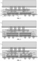
- FIG. 1 is a schematic diagram of a semiconductor package structure according to an embodiment of the present application.
- the semiconductor package structure includes a first package structure and a second package structure.
- the first package structure includes an intermediary layer 30 and a molding compound 40.
- a plurality of first connection pads 31 are disposed on the intermediary layer 30.
- the molding compound 40 wraps the intermediary layer 30 and is coplanar to the plurality of first connection pads 31.
- the second package structure 70 is disposed on the intermediary layer 30 and electrically connected to the plurality of first connection pads 31.
- a gap is formed between the first package structure and the second package structure 70.
- the first package structure can be connected to the second package structure by means of the intermediary layer.
- the interconnection among package structures with different capacities can be achieved, so as to cause a combination among different package structures to be more flexible. Therefore, the semiconductor package structure is applicable to different application scenarios.
- the first package structure and the second package structure are independently packaged, the first package structure and the second package structure may be respectively tested, so that failure analysis can be performed more rapidly. Therefore, after the semiconductor package structure is assembled, testing may not be required to be performed on the entire structure. Since there is a gap between the second package structure and the first package structure, the spacing between the second package structure and the first package structure can be increased.
- the second package structure is detachably disposed on the first package structure, so that the utilization rate of the first package structure can be enhanced by disposing the second package structure with different capacity on the first package structure.
- the first package structure further includes: a base plate 10; at least one first chip stack body 21, disposed on the base plate 10; and at least one second chip stack body 22, disposed on the base plate 10 and spaced apart from the at least one first chip stack body 21.
- the intermediary layer 30 is disposed on the first chip stack body 21 and the second chip stack body 22.
- the first chip stack body and the second chip stack body are connected with each other by means of the intermediary layer, so that the number of wire bonding can be decreased, and a wire bonding process can be simplified.
- the base plate 10 may be a redistribution base plate.
- the base plate 10 includes a base plate substrate 11, a base plate upper insulating dielectric layer 12 disposed on an upper surface of the base plate substrate 11, and a base plate lower insulating dielectric layer 13 disposed on a lower surface of the base plate substrate 11.
- the base plate substrate 11 may be a silicon substrate, a germanium substrate, a silicon germanium substrate, a silicon carbide substrate, an Silicon On Insulator, SOI substrate, or a Germanium On Insulator, GOI substrate, or may be a substrate including other element semiconductors or compound semiconductors, such as a glass substrate or a III-V compound substrates (for example, a gallium nitride substrate or a gallium arsenide substrate), or may be a stack of layer structures such as Si/SiGe, or may be other epitaxial structures such as Silicon Germanium On Insulator, SGOI.
- Each of the base plate upper insulating dielectric layer 12 and the base plate lower insulating dielectric layer 13 may be a solder mask layer.
- each of the material of the base plate upper insulating dielectric layer 12 and the material of the base plate lower insulating dielectric layer 13 may be green paint.
- the base plate 10 further includes a base plate upper connection pad 14 located in the base plate upper insulating dielectric layer 12, a base plate lower connection pad 15 located in the base plate lower insulating dielectric layer 13, and a base plate connection via 16 which penetrates through the base plate substrate 11 and which connects the base plate upper connection pad 14 and the base plate lower connection pad 15 with each other.
- Each of the material of the base plate upper connection pad 14 and the material of the base plate lower connection pad 15 may include at least one of aluminum, copper, nickel, tungsten, platinum, or gold.
- the base plate connection via 16 may be a Through-Silicon-Via, TSV.
- the base plate upper connection pad 14 is connected to the base plate lower connection pad 15 by means of the base plate connection via 16, so that a signal can be transmitted.
- two adjacent base plate upper connection pads 14 may also be connected with each other by means of a re-distribution layer, so that the transmission of the signal on the base plate can be completed.
- the base plate 10 further includes a base plate connection bump 17.
- the base plate connection bump 17 may electrically connect the semiconductor package structure to an external apparatus, so that at least one of a control signal, a power signal or a grounding signal that is configured to operate the chip stack body may be received from the external apparatus, or a data signal to be stored in the chip stack body may be received from the external apparatus, or data in the chip stack body may also be provided to the external apparatus.
- the base plate connection bump 17 includes a conductive material.
- the base plate connection bump 17 is a solder ball. It is to be understood that a shape of the base plate connection bump provided in this embodiment of the present application is only an inferior and feasible specific implementation in the embodiments of the present application, and does not constitute a limitation of the present application.
- the base plate connection bump may also be a structure with other shapes. The number, spacing, and location of the base plate connection bumps are not limited to any specific arrangement, and various modifications may be made.
- the first chip stack body 21 and the second chip stack body 22 are disposed on the base plate 10 by means of a bonding layer 60.
- Chips in the first chip stack body 21 and chips in the second chip stack body 22 may be Dynamic Random Access Memory, DRAM chips, Static Random Access Memory, SRAM chips, flash memory chips, Electrically Erasable Programmable Read-Only Memory, EEPROM chips, Phase-change Random Access Memory, PRAM chips, Magnetic Random Access Memory, MRAM chips, or Resistive Random Access Memory, RRAM chips.
- the bonding layer 60 may be a DAF film.
- the bonding layer includes a first bonding layer 61 and a second bonding layer 62 located on the first bonding layer 61.
- An elastic modulus of the second bonding layer 62 is greater than an elastic modulus of the first bonding layer 61.
- the first bonding layer since the first bonding layer is connected to the base plate, the first bonding layer mainly achieves a bonding effect. Since the second bonding layer is connected to the chips, the second bonding layer mainly achieves an effect of preventing the chip from warping. Since the elastic modulus of the second bonding layer is relatively high, warping does not occur during cutting. The first bonding layer has the relatively low elastic modulus, the bonding between the base plate and the chips will not be affected during the subsequent processes.
- the base plate 10 further includes a virtual channel 18.
- the bonding layer 60 is located on the virtual channel 18. A heat conductivity coefficient of the virtual channel 18 is greater than a heat conductivity coefficient of the bonding layer 60.
- the heat conductivity coefficient of the virtual channel is greater than the heat conductivity coefficient of the bonding layer, more heat generated by the operation of the chips can be dissipated by means of the virtual channel. Therefore, a heat dissipation capacity can be enhanced, and the impact on the performance of the device can be reduced.
- the virtual channel 18 is composed of the base plate upper connection pad 14, the base plate lower connection pad 15 and the base plate connection via 16. However, the base plate connection bump 17 is not formed below the virtual channel 18, so that signal transmission cannot be achieved, and only heat dissipation is performed.
- the heat conductivity coefficient of the virtual channel is greater than heat conductivity coefficients of other structures each composed of the base plate upper connection pad 14, the base plate lower connection pad 15 and the base plate connection via 16 for signal transmission, so that the impact of heat on signal transmission can be reduced.
- the first chip stack body 21 includes a first chip 210.
- the second chip stack body 22 includes a second chip 220.
- the first chip 210 is electrically connected to the second chip 220 by means of the intermediary layer 30.
- the first chip 210 or the second chip 220 is connected to the base plate 10 by means of a lead wire 50.
- the first chip 210 is connected to the second chip 220 by means of the intermediary layer 30, and the first chip 210 is connected to the base plate 10 by means of the lead wire 50, so that the second chip 220 is connected to the base plate 10 indirectly.
- the second chip is connected to the base plate by means of a lead wire, so that the first chip is connected to the base plate indirectly.
- wire bonding may be performed only on one of the first chip and the second chip, so that the wire bonding process can be simplified.
- FIG. 2 is a schematic diagram of a semiconductor package structure according to another embodiment of the present application.
- FIG. 3 is a schematic diagram of a semiconductor package structure according to still another embodiment of the present application.
- the first chip stack body 21 includes a first lower chip 212 and a first upper chip 211 that are stacked onto one another.
- the second chip stack body 22 includes a second lower chip 222 and a second upper chip 221 that are stacked onto one another.
- the intermediary layer 30 is disposed on the first upper chip 211 and the second upper chip 221.
- the first upper chip 211 is electrically connected to the second upper chip 221 by means of the intermediary layer 30.
- the first upper chip 211 or the second upper chip 221 is connected to the base plate 10 by means of the lead wire 50.
- Each of the first lower chip 212 and the second lower chip 222 is connected to the base plate 10 by means of a lead wire 50 respectively.
- the first upper chip 211 is connected to the second upper chip 221 by means of the intermediary layer 30, and the first upper chip 211 is connected to the base plate 10 by means of the lead wire 50, so that the second upper chip 221 is connected to the base plate 10 indirectly.
- the second upper chip is connected to the base plate by means of the lead wire, so that the first upper chip is connected to the base plate indirectly.
- the first lower chip 212 is electrically connected to the first upper chip 211; and the second lower chip 222 is electrically connected to the second upper chip 221.
- first lower chip 212 and the first upper chip 211 are connected with each other and the second lower chip 222 and the second upper chip 221 are connected with each other by means of a chip connection pad 202, a chip connection solder ball 203, and TSVs (not shown) located in the first upper chip 211 and the second upper chip 221.
- signal transmission may be directly performed between the first lower chip and the first upper chip, and signal transmission may be directly performed between the second lower chip and the second upper chip.
- signal transmission may also be performed between the first upper chip and the second upper chip by means of the intermediary layer. Therefore, wire bonding may be performed on the four chips for only once, thereby reducing the wire bonding process and reducing cost.
- the intermediary layer 30 includes: a first surface, where the plurality of first connection pads 31 are disposed on the first surface; a second surface, disposed opposite to the first surface, where a plurality of second connection pads 32 are disposed on the second surface; and a plurality of signal channels 33, configured to connect the plurality of first connection pads 31 and the plurality of second connection pads 32 with each other.
- Each of the material of the plurality of first connection pads 31 and the material of the plurality of second connection pads 32 may include at least one of aluminum, copper, nickel, tungsten, platinum, or gold.
- the intermediary layer 30 includes an intermediary substrate 302, an intermediary upper insulating dielectric layer 301 located on an upper surface of the intermediary substrate 302, and an intermediary lower insulating dielectric layer 303 located on a lower surface of the intermediary substrate 302.
- the plurality of first connection pads 31 are located in the intermediary upper insulating dielectric layer 301, and the plurality of second connection pads 32 are located in the intermediary lower insulating dielectric layer 303.
- the intermediary substrate may be a silicon substrate, a germanium substrate, a silicon germanium substrate, a silicon carbide substrate, an Silicon On Insulator, SOI substrate, or a Germanium On Insulator, GOI substrate, or may be a substrate including other element semiconductors or compound semiconductors, such as a glass substrate or a III-V compound substrates (for example, a gallium nitride substrate or a gallium arsenide substrate), or may be a stack of layer structures such as Si/SiGe, or may be other epitaxial structures such as Silicon Germanium On Insulator, SGOI.
- Each of the intermediary upper insulating dielectric layer 301 and the intermediary lower insulating dielectric layer 303 may be a solder mask layer.
- each of the material of the intermediary upper insulating dielectric layer and the material of the intermediary lower insulating dielectric layer may be green paint.
- the first chip stack body 21 and the second chip stack body 22 include a plurality of lead wire pads 201.
- the plurality of lead wire pads 201 are connected to the plurality of second connection pads 32 by means of a re-distribution layer.
- the re-distribution layer (not shown) may be located on a surface of the first chip stack body and a surface of the second chip stack body, or may be located inside the first chip stack body and the second chip stack body.
- a plurality of first solder balls 34 are formed between the plurality of second connection pads 32 and the plurality of lead wire pads 201.
- the plurality of lead wire pads 201 on the first chip stack body 21 and the second chip stack body 22 are connected to the plurality of second connection pads 32 by means of the plurality of first solder balls 34.
- the plurality of second connection pads 32 connected to the first chip stack body 21 and the second chip stack body 22 are connected to each other by means of a re-distribution layer.
- the re-distribution layer may be located on a surface of the intermediary layer, or may be located inside the intermediary layer.
- the molding compound 40 is coplanar with the plurality of first connection pads 31. In this way, after the second package structure is connected to the first package structure, there may be a large gap between the first package structure and the second package structure, so that the heat dissipation efficiency of the second package structure can be guaranteed.
- the gap between the first package structure and the second package structure is reduced, which does not facilitate heat dissipation and the filling of a filling layer when the filling layer is formed subsequently. If the surface of each of the plurality of first connection pads is higher than the surface of the molding compound, the gap may be increased, but the molding compound may not cover a bonding wire, so that the bonding wire is exposed, which does not facilitate the protection of the bonding wire.
- the second package structure 70 includes a second solder ball 71.
- the second solder ball 71 is electrically connected to the plurality of first connection pads 31 located on the intermediary layer 30.
- the second package structure 70 may be a Universal File Store, UFS chip.
- the second package structure 70 further includes a second base plate 72.
- the structure of the second base plate 72 may be the same as the structure of the base plate 10, which is not described herein again.
- the second solder ball 71 is located on the second base plate 72.
- FIG. 4 is a schematic diagram of a semiconductor package structure according to another embodiment of the present application. As shown in FIG. 4 , the semiconductor package structure further includes a filling layer 80. The gap is fully filled with the filling layer 80.
- a heat conductivity coefficient of the filling layer 80 is greater than a heat conductivity coefficient of the molding compound 40.
- a sealed interface may be formed between the first package structure and the second package structure, so as to reduce the contact of metal structures of the first package structure and the second package structure with external air or other materials, and heat conduction can be achieved as well. Since the heat conductivity coefficient of the filling layer is relatively large, more heat can be dissipated from the filling layer, so that the impact of the heat on the first package structure can be reduced. Although the heat conductivity coefficient of the filling layer is relatively large, since a thermal expansion coefficient of the filling layer matches with a thermal expansion coefficient of the first package structure and a thermal expansion coefficient of the second package structure, the change in the volume of the filling layer is small. Therefore, no outward pressure is generated on the first package structure and the second package structure, and the stability of the structure can be guaranteed.
- the filling layer 80 is filled with a carbon nanotube filler, so that more heat can be absorbed from the second package structure. Therefore, the impact of the heat on the first package structure can be reduced.
- the volume of a filler in the filling layer 80 is less than the volume of a filler in the molding compound 40.
- the filler in the molding compound 40 is a first filler 401
- the filler in the filling layer 80 is a second filler 801.
- the volume of the second filler 801 is less than the volume of the first filler 401.
- Each of a main material of the molding compound 40 and a main material of the filling layer 80 may be epoxy resin, and each of the filler in the molding compound and the filler in the filling layer may be silicon dioxide.
- the filling layer with large fluidity is selected.
- the volume of the filler in the filling layer is small, and the fluidity of the main material of the filling layer is large.
- the semiconductor package structure provided in the embodiments of the present application is applicable to UFS Multi Chip Package, UMCP of a Package on Package, PoP structure.
- An embodiment of the present application further provides a method for manufacturing a semiconductor package structure.
- the method includes the following operations.
- a first package structure is provided, where the first package structure includes an intermediary layer and a molding compound, a plurality of first connection pads are disposed on the intermediary layer, and the molding compound wraps the intermediary layer and is coplanar to the plurality of first connection pads.
- a second package structure is provided, where the second package structure is disposed on the intermediary layer and electrically connected to the plurality of first connection pads, and a gap is formed between the first package structure and the second package structure.
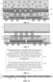
- FIG. 7a to FIG. 7g are schematic diagrams of a semiconductor package structure during manufacturing according to an embodiment of the present application.
- the first package structure includes an intermediary layer 30 and a molding compound 40.
- a plurality of first connection pads 31 are disposed on the intermediary layer 30.
- the molding compound 40 wraps the intermediary layer 30 and is coplanar to the plurality of first connection pads 31.
- the base plate 10 is provided.
- the base plate 10 may be a redistribution base plate.
- the base plate 10 includes a base plate substrate 11, a base plate upper insulating dielectric layer 12 disposed on an upper surface of the base plate substrate 11, and a base plate lower insulating dielectric layer 13 disposed on a lower surface of the base plate substrate 11.
- the base plate substrate 11 may be a silicon substrate, a germanium substrate, a silicon germanium substrate, a silicon carbide substrate, an Silicon On Insulator, SOI substrate, or a Germanium On Insulator, GOI substrate, or may be a substrate including other element semiconductors or compound semiconductors, such as a glass substrate or a III-V compound substrates (for example, a gallium nitride substrate or a gallium arsenide substrate), or may be a stack of layer structures such as Si/SiGe, or may be other epitaxial structures such as Silicon Germanium On Insulator, SGOI.
- Each of the base plate upper insulating dielectric layer 12 and the base plate lower insulating dielectric layer 13 may be a solder mask layer.
- each of the material of the base plate upper insulating dielectric layer 12 and the material of the base plate lower insulating dielectric layer 13 may be green paint.
- the base plate 10 further includes a base plate upper connection pad 14 located in the base plate upper insulating dielectric layer 12, a base plate lower connection pad 15 located in the base plate lower insulating dielectric layer 13, and a base plate connection via 16 which penetrates through the base plate substrate 11 and which connects the base plate upper connection pad 14 and the base plate lower connection pad 15 with each other.
- Each of the material of the base plate upper connection pad 14 and the material of the base plate lower connection pad 15 may include at least one of aluminum, copper, nickel, tungsten, platinum, or gold.
- the base plate connection via 16 may be a TSV.
- the base plate upper connection pad 14 is connected to the base plate lower connection pad 15 by means of the base plate connection via 16, so that a signal can be transmitted.
- two adjacent base plate upper connection pads 14 may also be connected with each other by means of a re-distribution layer, so that the transmission of the signal on the base plate can be completed.
- the base plate 10 further includes a virtual channel 18.
- the virtual channel 18 is composed of the base plate upper connection pad 14, the base plate lower connection pad 15 and the base plate connection via 16.
- the base plate connection bump is not formed below the virtual channel 18, so that signal transmission cannot be achieved, and only heat dissipation is performed.
- the heat conductivity coefficient of the virtual channel is greater than heat conductivity coefficients of other structures each composed of the base plate upper connection pad 14, the base plate lower connection pad 15 and the base plate connection via 16 for signal transmission, so that the impact of heat on signal transmission can be reduced.
- At least one first chip stack body 21 and at least one second chip stack body 22 are formed on the base plate 10.
- the first chip stack body 21 is spaced apart from the second chip stack body 22.
- a bonding layer 60 is first formed on the base plate 10, and then the first chip stack body 21 and the second chip stack body 22 are formed on the bonding layer 60.
- the bonding layer 60 may be a DAF film.
- the bonding layer 60 includes a first bonding layer 61 and a second bonding layer 62 located on the first bonding layer 61.
- An elastic modulus of the second bonding layer 62 is greater than an elastic modulus of the first bonding layer 61.
- the first bonding layer since the first bonding layer is connected to the base plate, the first bonding layer mainly achieves a bonding effect. Since the second bonding layer is connected to the chips, the second bonding layer mainly achieves an effect of preventing the chip from warping. Since the elastic modulus of the second bonding layer is relatively high, warping does not occur during cutting. The first bonding layer has the relatively low elastic modulus, the bonding between the base plate and the chips will not be affected during the subsequent processes.
- the bonding layer 60 is located on the virtual channel 18.
- a heat conductivity coefficient of the virtual channel 18 is greater than a heat conductivity coefficient of the bonding layer 60.
- the heat conductivity coefficient of the virtual channel is greater than the heat conductivity coefficient of the bonding layer, more heat generated by the operation of the chips can be dissipated by means of the virtual channel. Therefore, a heat dissipation capacity can be enhanced, and the impact on the performance of the device can be reduced.
- a plurality of lead wire pads 201 are formed on the first chip stack body 21 and the second chip stack body 22.
- the plurality of lead wire pads 201 may be connected to a plurality of second connection pads located on a subsequently formed intermediary layer by means of a re-distribution layer.
- an intermediary layer 30 is formed on the first chip stack body 21 and the second chip stack body 22.
- a carrier band 2 is pasted on a circular ring 1.
- the intermediary layer is then pasted on the carrier band 2.
- the entire intermediary layer is in a whole strip shape.
- the intermediary layer is cut to form units one by one shown in FIG. 7c .
- a surface of the intermediary layer on which the intermediary upper insulating dielectric layer is formed is pasted on the carrier band, and a plurality of first solder balls are formed on a surface of the intermediary layer on which the intermediary lower insulating dielectric layer is formed.
- the intermediary layer 30 is disposed on the first chip stack body 21 and the second chip stack body 22 in an inverted manner, so that the plurality of first solder balls 34 are connected to the first chip stack body 21 and the second chip stack body 22.
- the number of wire bonding can be decreased, and a wire bonding process can be simplified.
- the intermediary layer 30 includes: a first surface, where the plurality of first connection pads 31 are disposed on the first surface; a second surface, disposed opposite to the first surface, where the plurality of second connection pads 32 are disposed on the second surface; and a plurality of signal channels 33, configured to connect the plurality of first connection pads 31 and the plurality of second connection pads 32 with each other.
- Each of the material of the plurality of first connection pads 31 and the material of the plurality of second connection pads 32 may include at least one of aluminum, copper, nickel, tungsten, platinum, or gold.
- the intermediary layer 30 further includes an intermediary substrate 302, an intermediary upper insulating dielectric layer 301 located on an upper surface of the intermediary substrate 302, and an intermediary lower insulating dielectric layer 303 located on a lower surface of the intermediary substrate 302.
- the plurality of first connection pads 31 are located in the intermediary upper insulating dielectric layer 301, and the plurality of second connection pads 32 are located in the intermediary lower insulating dielectric layer 303.
- the first chip stack body includes one first chip 210.
- the second chip stack body 22 includes one second chip 220.
- the first chip 210 is electrically connected to the second chip 220 by means of the intermediary layer 30.
- the first chip 210 or the second chip 220 is connected to the base plate 10 by means of a lead wire 50.
- the first chip 210 is connected to the second chip 220 by means of the intermediary layer 30, and the first chip 210 is connected to the base plate 10 by means of the lead wire 50, so that the second chip 220 is connected to the base plate 10 indirectly.
- the second chip is connected to the base plate by means of the lead wire, so that the first chip is connected to the base plate indirectly.
- wire bonding since signal transmission between the first chip and the second chip is achieved by means of the intermediary layer, wire bonding may be performed only on one of the first chip and the second chip, so that the wire bonding process can be simplified.
- FIG. 7a to FIG. 7g only show the method for manufacturing a semiconductor package structure in which the first chip stack body includes one first chip, and the second chip stack body includes one second chip, but each of the first chip stack body and the second chip stack body may also include other stack structures.
- the first chip stack body 21 includes a first lower chip 212 and a first upper chip 211 that are stacked onto one another.
- the second chip stack body 22 includes a second lower chip 222 and a second upper chip 221 that are stacked onto one another.
- the intermediary layer 30 is disposed on the first upper chip 211 and the second upper chip 221.
- the first upper chip 211 is electrically connected to the second upper chip 221 by means of the intermediary layer 30.
- the first upper chip 211 or the second upper chip 221 is connected to the base plate 10 by means of the lead wire 50.
- Each of the first lower chip 212 and the second lower chip 222 is connected to the base plate 10 by means of a lead wire 50 respectively.
- the first upper chip 211 is connected to the second upper chip 221 by means of the intermediary layer 30, and the first upper chip 211 is connected to the base plate 10 by means of the lead wire 50, so that the second upper chip 221 is connected to the base plate 10 indirectly.
- the second upper chip is connected to the base plate by means of the lead wire, so that the first upper chip is connected to the base plate indirectly.
- the first lower chip 212 is electrically connected to the first upper chip 211; and the second lower chip 222 is electrically connected to the second upper chip 221.
- first lower chip 212 and the first upper chip 211 are connected with each other and the second lower chip 222 and the second upper chip 221 are connected with each other by means of a chip connection pad 202, a chip connection solder ball 203, and TSVs (not shown) located in the first upper chip 211 and the second upper chip 221.
- signal transmission may be directly performed between the first lower chip and the first upper chip, and signal transmission may be directly performed between the second lower chip and the second upper chip.
- signal transmission may also be performed between the first upper chip and the second upper chip by means of the intermediary layer. Therefore, wire bonding may be performed on the four chips for only once, thereby reducing the wire bonding process and reducing cost.
- the plurality of second connection pads 32 connected to the first chip stack body 21 and the second chip stack body 22 are connected to each other by means of a re-distribution layer.
- the re-distribution layer may be located on a surface of the intermediary layer, or may be located inside the intermediary layer.
- a molding compound 40 wrapping the first chip stack body 21, the second chip stack body 22 and the intermediary layer 30 is formed.
- the finally formed molding compound is coplanar to the plurality of first connection pads of the intermediary layer, during the formation of the molding compound, a profiled mold is not required, but only a mold with a normal shape is required. Since the mold with the normal shape is simple in shape, a manufacturing process is simple, and cost is relatively low.
- the gap between the first package structure and the second package structure is reduced, which does not facilitate heat dissipation and the filling of a filling layer when the filling layer is formed subsequently. If the surface of each of the plurality of first connection pads is higher than the surface of the molding compound, the gap may be increased, but the molding compound may not cover a bonding wire, so that the bonding wire is exposed, which does not facilitate the protection of the bonding wire.
- a base plate connection bump 17 is formed on the base plate lower connection pad 15 of the base plate 10.
- the base plate connection bump 17 includes a conductive material.
- S602 is executed, where the second package structure 70 is provided.
- the second package structure 70 is disposed on the intermediary layer 30 and electrically connected to the plurality of first connection pads 31.
- a gap is formed between the first package structure and the second package structure 70.
- a second solder ball 71 is formed on the second package structure 70.
- the second solder ball 71 is electrically connected to the plurality of first connection pads 31 located on the intermediary layer 30.
- the second package structure further includes a second base plate 72.
- the structure of the second base plate 72 may be the same as the structure of the base plate 10, which is not described herein again.
- the second solder ball 71 is located on the second base plate 72.
- a filling layer 80 is formed in the gap between the first package structure and the second package structure 70.
- a heat conductivity coefficient of the filling layer 80 is greater than a heat conductivity coefficient of the molding compound 40.
- a sealed interface may be formed between the first package structure and the second package structure, so as to reduce the contact of metal structures of the first package structure and the second package structure with external air or other materials, and heat conduction can be achieved as well. Since the heat conductivity coefficient of the filling layer is relatively large, more heat can be dissipated from the filling layer, so that the impact of the heat on the first package structure can be reduced. In addition, since a thermal expansion coefficient of the filling layer matches with a thermal expansion coefficient of the first package structure and a thermal expansion coefficient of the second package structure, the change in the volume of the filling layer is small. Therefore, no outward pressure is generated on the first package structure and the second package structure, and the stability of the structure can be guaranteed.
- the volume of a filler in the filling layer 80 is less than the volume of a filler in the molding compound 40.
- the filler in the molding compound 40 is a first filler 401
- the filler in the filling layer 80 is a second filler 801.
- the volume of the second filler 801 is less than the volume of the first filler 401.
- Each of a main material of the molding compound 40 and a main material of the filling layer 80 may be epoxy resin, and each of the filler in the molding compound and the filler in the filling layer may be silicon dioxide.
- the filling layer with large fluidity is selected.
- the volume of the filler in the filling layer is small, and the fluidity of the main material of the filling layer is large.
- the first package structure can be connected to the second package structure by means of the intermediary layer.
- the interconnection among package structures with different capacities can be achieved, so as to cause a combination among different package structures to be more flexible. Therefore, the semiconductor package structure is applicable to different application scenarios.
- the first package structure and the second package structure are independently packaged, the first package structure and the second package structure may be respectively tested, so that failure analysis can be performed more rapidly. Therefore, after the semiconductor package structure is assembled, testing may not be required to be performed on the entire structure. Since there is a gap between the second package structure and the first package structure, the spacing between the second package structure and the first package structure can be increased. Therefore, the heat dissipation efficiency of the second package structure can be enhanced, and the impact of heat on chips can be reduced.
Landscapes
- Engineering & Computer Science (AREA)
- Semiconductor Integrated Circuits (AREA)
- Wire Bonding (AREA)
- Chemical & Material Sciences (AREA)
- Materials Engineering (AREA)
- Manufacturing & Machinery (AREA)
- Physics & Mathematics (AREA)
- Geometry (AREA)
- Microelectronics & Electronic Packaging (AREA)
Abstract
Description
- This application is based upon and claims priority to
Chinese Patent Application No. 202210853472.6, filed on July 8, 2022 - The present application relates to the technical field of semiconductors, and in particular, to a semiconductor package structure and a manufacturing method.
- All sectors, industries and regions continually require lighter, faster, smaller, more functional, more reliable and more cost-effective products for the electronics industry. In order to meet these growing requirements of many different consumers, more circuits are required to be integrated to provide required functions. In almost all applications, there is a growing requirement for reducing dimensions, enhancing performance and improving the functions of the integrated circuits.
- In view of this, embodiments of the present application provide a semiconductor package structure and a manufacturing method.
- A first aspect of an embodiment of the present application provides a semiconductor package structure, including:
- a first package structure, including an intermediary layer and a molding compound, where a plurality of first connection pads are disposed on the intermediary layer, and the molding compound wraps the intermediary layer and is coplanar to the plurality of first connection pads; and
- a second package structure, disposed on the intermediary layer and electrically connected to the plurality of first connection pads.
- A gap is formed between the first package structure and the second package structure.
- In some embodiments, the first package structure further includes:
- a base plate;
- at least one first chip stack body, disposed on the base plate; and
- at least one second chip stack body, disposed on the base plate and spaced apart from the first chip stack.
- The intermediary layer is disposed on the first chip stack body and the second chip stack body.
- In some embodiments, the first chip stack body includes one first chip, and the second chip stack body includes one second chip.
- The first chip is electrically connected to the second chip by means of the intermediary layer.
- In some embodiments, the first chip or the second chip is connected to the base plate by means of a lead wire.
- In some embodiments, the first chip stack body includes a first lower chip and a first upper chip that are stacked onto one another, and the second chip stack body includes a second lower chip and a second upper chip that are stacked onto one another.
- The intermediary layer is disposed on the first upper chip and the second upper chip. The first upper chip is electrically connected to the second upper chip by means of the intermediary layer.
- In some embodiments, the first upper chip or the second upper chip is connected to the base plate by means of a lead wire.
- In some embodiments, each of the first lower chip and the second lower chip is connected to the base plate by means of a lead wire respectively.
- In some embodiments, the first lower chip is electrically connected to the first upper chip, and the second lower chip is electrically connected to the second upper chip.
- In some embodiments, the intermediary layer includes a first surface, a second surface, and a plurality of signal channels.
- The plurality of first connection pads are disposed on the first surface.
- The second surface is disposed opposite to the first surface. A plurality of second connection pads are disposed on the second surface.
- The plurality of signal channels are configured to connect the plurality of first connection pads and plurality of the second connection pads with each other.
- In some embodiments, the first chip stack body and the second chip stack body include a plurality of lead wire pads. The plurality of lead wire pads are connected to the plurality of second connection pads by means of a re-distribution layer.
- In some embodiments, the plurality of second connection pads connected to the first chip stack body and the second chip stack body are connected to each other by means of a re-distribution layer.
- In some embodiments, the first chip stack body and the second chip stack body are disposed on the base plate by means of a bonding layer.
- In some embodiments, the base plate includes a virtual channel. The bonding layer is located on the virtual channel. A heat conductivity coefficient of the virtual channel is greater than a heat conductivity coefficient of the bonding layer.
- In some embodiments, the semiconductor package structure further includes a filling layer. The gap is fully filled with the filling layer.
- In some embodiments, a heat conductivity coefficient of the filling layer is greater than a heat conductivity coefficient of the molding compound.
- In some embodiments, a volume of a filler in the filling layer is less than a volume of a filler in the molding compound.
- In some embodiments, the bonding layer includes a first bonding layer and a second bonding layer. The second bonding layer is located on the first bonding layer. An elastic modulus of the second bonding layer is greater than an elastic modulus of the first bonding layer.
- A second aspect of an embodiment of the present application provides a method for manufacturing a semiconductor package structure, including the following operations.
- A first package structure is provided. The first package structure includes an intermediary layer and a molding compound. A plurality of first connection pads are disposed on the intermediary layer. The molding compound wraps the intermediary layer and is coplanar to the plurality of first connection pads.
- A second package structure is provided. The second package structure is disposed on the intermediary layer and electrically connected to the plurality of first connection pads.
- A gap is formed between the first package structure and the second package structure.
- In the embodiments of the present application, through the arrangement of the intermediary layer, the first package structure can be connected to the second package structure by means of the intermediary layer. In this way, the interconnection among package structures with different capacities can be achieved, so as to cause a combination among different package structures to be more flexible. Therefore, the semiconductor package structure is applicable to different application scenarios. In addition, since the first package structure and the second package structure are independently packaged, the first package structure and the second package structure may be respectively tested, so that failure analysis can be performed more rapidly. Therefore, after the semiconductor package structure is assembled, testing may not be required to be performed on the entire structure. Since there is a gap between the second package structure and the first package structure, the spacing between the second package structure and the first package structure can be increased. Therefore, the heat dissipation efficiency of the second package structure can be enhanced, and the impact of heat on chips can be reduced.
- In order to more clearly illustrate the technical solutions in the embodiments of the present application or conventional technologies, the drawings used in the technical description of the embodiments will be briefly described below. It is apparent that the drawings in the following descriptions are merely some embodiments of the present application. Other drawings can be obtained from those skilled in the art according to these drawings without any creative work.
-
FIG. 1 is a schematic diagram of a semiconductor package structure according to an embodiment of the present application. -
FIG. 2 to FIG. 5 are other examples of a semiconductor package structure according to an embodiment of the present application. -
FIG. 6 is a schematic flowchart of a method for manufacturing a semiconductor package structure according to an embodiment of the present application. -
FIG. 7a to FIG. 7g are schematic diagrams of a device structure of a semiconductor package structure during manufacturing according to an embodiment of the present application. -
- 1-Circular ring; 2-Carrier band;
- 10-Base plate; 11-Base plate substrate; 12-Base plate upper insulating dielectric layer; 13-Base plate lower insulating dielectric layer; 14-Base plate upper connection pad; 15-Base plate lower connection pad; 16-Base plate connection via; 17-Base plate connection bump; 18-Virtual channel;
- 21-First chip stack body; 22-Second chip stack body; 210-First chip; 220-Second chip; 211-First upper chip; 212-First lower chip; 221-Second upper chip; 222-Second lower chip; 201-Lead wire pad; 202-Chip connection pad; 203-Chip connection solder ball;
- 30-Intermediary layer; 31-First connection pad; 32-Second connection pad; 33-Signal channel; 34-First solder ball; 301-Intermediary upper insulating dielectric layer; 302-Intermediary substrate; 303-Intermediary lower insulating dielectric layer;
- 40-Molding compound; 401-First filler;
- 50-Lead wire;
- 60-Bonding layer; 61-First bonding layer; 62-Second bonding layer;
- 70-Second package structure; 71-Second solder ball; 72-Second base plate;
- 80-Filling layer; 801-Second filler.
- Exemplary embodiments disclosed in the present application are described in more detail with reference to drawings. Although the exemplary embodiments of the present application are shown in the drawings, it should be understood that the present application may be implemented in various forms and should not be limited by the specific embodiments described here. On the contrary, these embodiments are provided for more thorough understanding of the present application, and to fully convey a scope disclosed in the embodiments of the present application to a person skilled in the art.
- In the following descriptions, a lot of specific details are given in order to provide the more thorough understanding of the present application. However, it is apparent to a person skilled in the art that the present application may be implemented without one or more of these details. In other examples, in order to avoid confusion with the present application, some technical features well-known in the field are not described. Namely, all the features of the actual embodiments are not described here, and well-known functions and structures are not described in detail.
- In the drawings, the dimensions of a layer, a region, and an element and their relative dimensions may be exaggerated for clarity. The same reference numeral represents the same element throughout the description.
- It should be understood that while the element or the layer is referred to as being "on", "adjacent to", "connected to" or "coupled to" other elements or layers, it may be directly on the other elements or layers, adjacent to, connected or coupled to the other elements or layers, or an intermediate element or layer may be existent. In contrast, while the element is referred to as being "directly on", "directly adjacent to", "directly connected to" or "directly coupled to" other elements or layers, the intermediate element or layer is not existent. It should be understood that although terms first, second, third and the like may be used to describe various elements, components, regions, layers and/or sections, these elements, components, regions, layers and/or sections should not be limited by these terms. These terms are only used to distinguish one element, component, region, layer or section from another element, component, region, layer or section. Therefore, without departing from the teaching of the present application, a first element, component, region, layer or section discussed below may be represented as a second element, component, region, layer or section. While the second element, component, region, layer or section is discussed, it does not mean that the first element, component, region, layer or section is necessarily existent in the present application.
- Spatial relationship terms, such as "under", "below", "lower", "underneath", "above", "upper" and the like, may be used here for conveniently describing so that a relationship between one element or feature shown in the drawings and other elements or features is described. It should be understood that in addition to orientations shown in the drawings, the spatial relationship terms are intended to further include the different orientations of a device in use and operation. For example, if the device in the drawings is turned over, then the elements or the features described as "below" or "underneath" or "under" other elements may be oriented "on" the other elements or features. Therefore, the exemplary terms "below" and "under" may include two orientations of up and down. The device may be otherwise oriented (rotated by 90 degrees or other orientations) and the spatial descriptions used here are interpreted accordingly.
- A purpose of the terms used here is only to describe the specific embodiments and not as limitation to the present application. While used here, singular forms of "a", "an" and "said/the" are also intended to include plural forms, unless the context clearly indicates otherwise. It should also be understood that terms "composition" and/or "including", while used in the description, determine the existence of the described features, integers, steps, operations, elements and/or components, but do not exclude the existence or addition of one or more other features, integers, steps, operations, elements, components, and/or groups. As used herein, a term "and/or" includes any and all combinations of related items listed.
- In order to understand the present application thoroughly, detailed operations and detailed structures are presented in the following description, so as to explain the technical solutions of the present application. Preferred embodiments of the present application are described in detail below. However, the present application may also have other implementations in addition to these detailed descriptions.
- An embodiment of the present application provides a semiconductor package structure.
FIG. 1 is a schematic diagram of a semiconductor package structure according to an embodiment of the present application. - With reference to
FIG. 1 , the semiconductor package structure includes a first package structure and a second package structure. - The first package structure includes an
intermediary layer 30 and amolding compound 40. A plurality offirst connection pads 31 are disposed on theintermediary layer 30. Themolding compound 40 wraps theintermediary layer 30 and is coplanar to the plurality offirst connection pads 31. - The
second package structure 70 is disposed on theintermediary layer 30 and electrically connected to the plurality offirst connection pads 31. - A gap is formed between the first package structure and the
second package structure 70. - In the embodiments of the present application, through the arrangement of the intermediary layer, the first package structure can be connected to the second package structure by means of the intermediary layer. In this way, the interconnection among package structures with different capacities can be achieved, so as to cause a combination among different package structures to be more flexible. Therefore, the semiconductor package structure is applicable to different application scenarios. In addition, since the first package structure and the second package structure are independently packaged, the first package structure and the second package structure may be respectively tested, so that failure analysis can be performed more rapidly. Therefore, after the semiconductor package structure is assembled, testing may not be required to be performed on the entire structure. Since there is a gap between the second package structure and the first package structure, the spacing between the second package structure and the first package structure can be increased. Therefore, the heat dissipation efficiency of the second package structure can be enhanced, and the impact of heat on a chip (the first package structure) can be reduced. The second package structure is detachably disposed on the first package structure, so that the utilization rate of the first package structure can be enhanced by disposing the second package structure with different capacity on the first package structure.
- In an embodiment, the first package structure further includes: a
base plate 10; at least one firstchip stack body 21, disposed on thebase plate 10; and at least one secondchip stack body 22, disposed on thebase plate 10 and spaced apart from the at least one firstchip stack body 21. Theintermediary layer 30 is disposed on the firstchip stack body 21 and the secondchip stack body 22. - In this embodiment of the present application, the first chip stack body and the second chip stack body are connected with each other by means of the intermediary layer, so that the number of wire bonding can be decreased, and a wire bonding process can be simplified.
- In some embodiments, the
base plate 10 may be a redistribution base plate. - The
base plate 10 includes abase plate substrate 11, a base plate upper insulatingdielectric layer 12 disposed on an upper surface of thebase plate substrate 11, and a base plate lower insulatingdielectric layer 13 disposed on a lower surface of thebase plate substrate 11. - The
base plate substrate 11 may be a silicon substrate, a germanium substrate, a silicon germanium substrate, a silicon carbide substrate, an Silicon On Insulator, SOI substrate, or a Germanium On Insulator, GOI substrate, or may be a substrate including other element semiconductors or compound semiconductors, such as a glass substrate or a III-V compound substrates (for example, a gallium nitride substrate or a gallium arsenide substrate), or may be a stack of layer structures such as Si/SiGe, or may be other epitaxial structures such as Silicon Germanium On Insulator, SGOI. - Each of the base plate upper insulating
dielectric layer 12 and the base plate lower insulatingdielectric layer 13 may be a solder mask layer. For example, each of the material of the base plate upper insulatingdielectric layer 12 and the material of the base plate lower insulatingdielectric layer 13 may be green paint. - The
base plate 10 further includes a base plateupper connection pad 14 located in the base plate upper insulatingdielectric layer 12, a base platelower connection pad 15 located in the base plate lower insulatingdielectric layer 13, and a base plate connection via 16 which penetrates through thebase plate substrate 11 and which connects the base plateupper connection pad 14 and the base platelower connection pad 15 with each other. - Each of the material of the base plate
upper connection pad 14 and the material of the base platelower connection pad 15 may include at least one of aluminum, copper, nickel, tungsten, platinum, or gold. The base plate connection via 16 may be a Through-Silicon-Via, TSV. - The base plate
upper connection pad 14 is connected to the base platelower connection pad 15 by means of the base plate connection via 16, so that a signal can be transmitted. In addition, two adjacent base plateupper connection pads 14 may also be connected with each other by means of a re-distribution layer, so that the transmission of the signal on the base plate can be completed. - The
base plate 10 further includes a baseplate connection bump 17. The baseplate connection bump 17 may electrically connect the semiconductor package structure to an external apparatus, so that at least one of a control signal, a power signal or a grounding signal that is configured to operate the chip stack body may be received from the external apparatus, or a data signal to be stored in the chip stack body may be received from the external apparatus, or data in the chip stack body may also be provided to the external apparatus. - The base
plate connection bump 17 includes a conductive material. In the embodiment of the present application, the baseplate connection bump 17 is a solder ball. It is to be understood that a shape of the base plate connection bump provided in this embodiment of the present application is only an inferior and feasible specific implementation in the embodiments of the present application, and does not constitute a limitation of the present application. The base plate connection bump may also be a structure with other shapes. The number, spacing, and location of the base plate connection bumps are not limited to any specific arrangement, and various modifications may be made. - In an embodiment, the first
chip stack body 21 and the secondchip stack body 22 are disposed on thebase plate 10 by means of abonding layer 60. - Chips in the first
chip stack body 21 and chips in the secondchip stack body 22 may be Dynamic Random Access Memory, DRAM chips, Static Random Access Memory, SRAM chips, flash memory chips, Electrically Erasable Programmable Read-Only Memory, EEPROM chips, Phase-change Random Access Memory, PRAM chips, Magnetic Random Access Memory, MRAM chips, or Resistive Random Access Memory, RRAM chips. - The
bonding layer 60 may be a DAF film. - In an embodiment, as shown in
FIG. 5 , the bonding layer includes afirst bonding layer 61 and asecond bonding layer 62 located on thefirst bonding layer 61. An elastic modulus of thesecond bonding layer 62 is greater than an elastic modulus of thefirst bonding layer 61. - In this embodiment of the present application, since the first bonding layer is connected to the base plate, the first bonding layer mainly achieves a bonding effect. Since the second bonding layer is connected to the chips, the second bonding layer mainly achieves an effect of preventing the chip from warping. Since the elastic modulus of the second bonding layer is relatively high, warping does not occur during cutting. The first bonding layer has the relatively low elastic modulus, the bonding between the base plate and the chips will not be affected during the subsequent processes. The
base plate 10 further includes avirtual channel 18. Thebonding layer 60 is located on thevirtual channel 18. A heat conductivity coefficient of thevirtual channel 18 is greater than a heat conductivity coefficient of thebonding layer 60. - In this embodiment of the present application, since the heat conductivity coefficient of the virtual channel is greater than the heat conductivity coefficient of the bonding layer, more heat generated by the operation of the chips can be dissipated by means of the virtual channel. Therefore, a heat dissipation capacity can be enhanced, and the impact on the performance of the device can be reduced.
- The
virtual channel 18 is composed of the base plateupper connection pad 14, the base platelower connection pad 15 and the base plate connection via 16. However, the baseplate connection bump 17 is not formed below thevirtual channel 18, so that signal transmission cannot be achieved, and only heat dissipation is performed. - In some embodiments, the heat conductivity coefficient of the virtual channel is greater than heat conductivity coefficients of other structures each composed of the base plate
upper connection pad 14, the base platelower connection pad 15 and the base plate connection via 16 for signal transmission, so that the impact of heat on signal transmission can be reduced. - As shown in
FIG. 1 , the firstchip stack body 21 includes afirst chip 210. The secondchip stack body 22 includes asecond chip 220. Thefirst chip 210 is electrically connected to thesecond chip 220 by means of theintermediary layer 30. - In an embodiment, the
first chip 210 or thesecond chip 220 is connected to thebase plate 10 by means of alead wire 50. - In the embodiment shown in
FIG. 1 , thefirst chip 210 is connected to thesecond chip 220 by means of theintermediary layer 30, and thefirst chip 210 is connected to thebase plate 10 by means of thelead wire 50, so that thesecond chip 220 is connected to thebase plate 10 indirectly. In other embodiments, the second chip is connected to the base plate by means of a lead wire, so that the first chip is connected to the base plate indirectly. - In this embodiment, since signal transmission between the first chip and the second chip is achieved by means of the intermediary layer, wire bonding may be performed only on one of the first chip and the second chip, so that the wire bonding process can be simplified.
-
FIG. 2 is a schematic diagram of a semiconductor package structure according to another embodiment of the present application.FIG. 3 is a schematic diagram of a semiconductor package structure according to still another embodiment of the present application. As shown inFIG. 2 and FIG. 3 , the firstchip stack body 21 includes a firstlower chip 212 and a firstupper chip 211 that are stacked onto one another. The secondchip stack body 22 includes a secondlower chip 222 and a secondupper chip 221 that are stacked onto one another. - The
intermediary layer 30 is disposed on the firstupper chip 211 and the secondupper chip 221. The firstupper chip 211 is electrically connected to the secondupper chip 221 by means of theintermediary layer 30. - In an embodiment, as shown in
FIG. 2 , the firstupper chip 211 or the secondupper chip 221 is connected to thebase plate 10 by means of thelead wire 50. - Each of the first
lower chip 212 and the secondlower chip 222 is connected to thebase plate 10 by means of alead wire 50 respectively. - In the embodiment shown in
FIG. 2 , the firstupper chip 211 is connected to the secondupper chip 221 by means of theintermediary layer 30, and the firstupper chip 211 is connected to thebase plate 10 by means of thelead wire 50, so that the secondupper chip 221 is connected to thebase plate 10 indirectly. In other embodiments, the second upper chip is connected to the base plate by means of the lead wire, so that the first upper chip is connected to the base plate indirectly. - In this embodiment, since signal transmission between the first upper chip and the second upper chip is achieved by means of the intermediary layer, wire bonding may be performed only on one of the first upper chip and the second upper chip, so that the wire bonding process can be simplified. In addition, since the first lower chip is isolated from the first upper chip and the second lower chip is isolated from the second upper chip by means of the bonding layer, signal transmission cannot be achieved, so that the first lower chip and the second lower chip are respectively connected to the base plate by means of wire bonding, so as to achieve signal transmission.
- In an embodiment, as shown in
FIG. 3 , the firstlower chip 212 is electrically connected to the firstupper chip 211; and the secondlower chip 222 is electrically connected to the secondupper chip 221. - Specifically, the first
lower chip 212 and the firstupper chip 211 are connected with each other and the secondlower chip 222 and the secondupper chip 221 are connected with each other by means of a chip connection pad 202, a chipconnection solder ball 203, and TSVs (not shown) located in the firstupper chip 211 and the secondupper chip 221. - In this embodiment, signal transmission may be directly performed between the first lower chip and the first upper chip, and signal transmission may be directly performed between the second lower chip and the second upper chip. In addition, signal transmission may also be performed between the first upper chip and the second upper chip by means of the intermediary layer. Therefore, wire bonding may be performed on the four chips for only once, thereby reducing the wire bonding process and reducing cost.
- In an embodiment, the
intermediary layer 30 includes: a first surface, where the plurality offirst connection pads 31 are disposed on the first surface; a second surface, disposed opposite to the first surface, where a plurality ofsecond connection pads 32 are disposed on the second surface; and a plurality ofsignal channels 33, configured to connect the plurality offirst connection pads 31 and the plurality ofsecond connection pads 32 with each other. - Each of the material of the plurality of
first connection pads 31 and the material of the plurality ofsecond connection pads 32 may include at least one of aluminum, copper, nickel, tungsten, platinum, or gold. - The
intermediary layer 30 includes anintermediary substrate 302, an intermediary upper insulatingdielectric layer 301 located on an upper surface of theintermediary substrate 302, and an intermediary lower insulatingdielectric layer 303 located on a lower surface of theintermediary substrate 302. The plurality offirst connection pads 31 are located in the intermediary upper insulatingdielectric layer 301, and the plurality ofsecond connection pads 32 are located in the intermediary lower insulatingdielectric layer 303. - The intermediary substrate may be a silicon substrate, a germanium substrate, a silicon germanium substrate, a silicon carbide substrate, an Silicon On Insulator, SOI substrate, or a Germanium On Insulator, GOI substrate, or may be a substrate including other element semiconductors or compound semiconductors, such as a glass substrate or a III-V compound substrates (for example, a gallium nitride substrate or a gallium arsenide substrate), or may be a stack of layer structures such as Si/SiGe, or may be other epitaxial structures such as Silicon Germanium On Insulator, SGOI.
- Each of the intermediary upper insulating
dielectric layer 301 and the intermediary lower insulatingdielectric layer 303 may be a solder mask layer. For example, each of the material of the intermediary upper insulating dielectric layer and the material of the intermediary lower insulating dielectric layer may be green paint. - In an embodiment, the first
chip stack body 21 and the secondchip stack body 22 include a plurality oflead wire pads 201. The plurality oflead wire pads 201 are connected to the plurality ofsecond connection pads 32 by means of a re-distribution layer. - In this embodiment, the re-distribution layer (not shown) may be located on a surface of the first chip stack body and a surface of the second chip stack body, or may be located inside the first chip stack body and the second chip stack body.
- As shown in
FIG. 1 , a plurality offirst solder balls 34 are formed between the plurality ofsecond connection pads 32 and the plurality oflead wire pads 201. The plurality oflead wire pads 201 on the firstchip stack body 21 and the secondchip stack body 22 are connected to the plurality ofsecond connection pads 32 by means of the plurality offirst solder balls 34. - In an embodiment, the plurality of
second connection pads 32 connected to the firstchip stack body 21 and the secondchip stack body 22 are connected to each other by means of a re-distribution layer. - In this embodiment, the re-distribution layer may be located on a surface of the intermediary layer, or may be located inside the intermediary layer.
- In an embodiment, the
molding compound 40 is coplanar with the plurality offirst connection pads 31. In this way, after the second package structure is connected to the first package structure, there may be a large gap between the first package structure and the second package structure, so that the heat dissipation efficiency of the second package structure can be guaranteed. - If a surface of the molding compound is higher than a surface of each of the plurality of first connection pads, the gap between the first package structure and the second package structure is reduced, which does not facilitate heat dissipation and the filling of a filling layer when the filling layer is formed subsequently. If the surface of each of the plurality of first connection pads is higher than the surface of the molding compound, the gap may be increased, but the molding compound may not cover a bonding wire, so that the bonding wire is exposed, which does not facilitate the protection of the bonding wire.
- In an embodiment, the
second package structure 70 includes asecond solder ball 71. Thesecond solder ball 71 is electrically connected to the plurality offirst connection pads 31 located on theintermediary layer 30. - The
second package structure 70 may be a Universal File Store, UFS chip. - The
second package structure 70 further includes asecond base plate 72. The structure of thesecond base plate 72 may be the same as the structure of thebase plate 10, which is not described herein again. - The
second solder ball 71 is located on thesecond base plate 72. -
FIG. 4 is a schematic diagram of a semiconductor package structure according to another embodiment of the present application. As shown inFIG. 4 , the semiconductor package structure further includes a filling layer 80. The gap is fully filled with the filling layer 80. - A heat conductivity coefficient of the filling layer 80 is greater than a heat conductivity coefficient of the
molding compound 40. - Through the arrangement of the filling layer, a sealed interface may be formed between the first package structure and the second package structure, so as to reduce the contact of metal structures of the first package structure and the second package structure with external air or other materials, and heat conduction can be achieved as well. Since the heat conductivity coefficient of the filling layer is relatively large, more heat can be dissipated from the filling layer, so that the impact of the heat on the first package structure can be reduced. Although the heat conductivity coefficient of the filling layer is relatively large, since a thermal expansion coefficient of the filling layer matches with a thermal expansion coefficient of the first package structure and a thermal expansion coefficient of the second package structure, the change in the volume of the filling layer is small. Therefore, no outward pressure is generated on the first package structure and the second package structure, and the stability of the structure can be guaranteed.
- In some embodiments, for example, the filling layer 80 is filled with a carbon nanotube filler, so that more heat can be absorbed from the second package structure. Therefore, the impact of the heat on the first package structure can be reduced.
- The volume of a filler in the filling layer 80 is less than the volume of a filler in the
molding compound 40. - As shown in
FIG. 4 , the filler in themolding compound 40 is afirst filler 401, and the filler in the filling layer 80 is asecond filler 801. The volume of thesecond filler 801 is less than the volume of thefirst filler 401. - Each of a main material of the
molding compound 40 and a main material of the filling layer 80 may be epoxy resin, and each of the filler in the molding compound and the filler in the filling layer may be silicon dioxide. - In this embodiment, since the gap filled by the molding compound is relatively large, and the gap between the first package structure and the second package structure is relatively small, the filling layer with large fluidity is selected. The volume of the filler in the filling layer is small, and the fluidity of the main material of the filling layer is large.
- The semiconductor package structure provided in the embodiments of the present application is applicable to UFS Multi Chip Package, UMCP of a Package on Package, PoP structure.
- An embodiment of the present application further provides a method for manufacturing a semiconductor package structure. With reference to
FIG. 6 for details, as shown in the figure, the method includes the following operations. - At S601, a first package structure is provided, where the first package structure includes an intermediary layer and a molding compound, a plurality of first connection pads are disposed on the intermediary layer, and the molding compound wraps the intermediary layer and is coplanar to the plurality of first connection pads.
- At S602, a second package structure is provided, where the second package structure is disposed on the intermediary layer and electrically connected to the plurality of first connection pads, and a gap is formed between the first package structure and the second package structure.
- The method for manufacturing the semiconductor package structure provided in the embodiments of the present application is further described in detail below with reference to specific embodiments.
-
FIG. 7a to FIG. 7g are schematic diagrams of a semiconductor package structure during manufacturing according to an embodiment of the present application. - First, with reference to
FIG. 7a to FIG. 7e , S601 is executed, where the first package structure is provided. The first package structure includes anintermediary layer 30 and amolding compound 40. A plurality offirst connection pads 31 are disposed on theintermediary layer 30. Themolding compound 40 wraps theintermediary layer 30 and is coplanar to the plurality offirst connection pads 31. - Specifically, with reference to
FIG. 7a first, thebase plate 10 is provided. - In some embodiments, the
base plate 10 may be a redistribution base plate. - The
base plate 10 includes abase plate substrate 11, a base plate upper insulatingdielectric layer 12 disposed on an upper surface of thebase plate substrate 11, and a base plate lower insulatingdielectric layer 13 disposed on a lower surface of thebase plate substrate 11. - The
base plate substrate 11 may be a silicon substrate, a germanium substrate, a silicon germanium substrate, a silicon carbide substrate, an Silicon On Insulator, SOI substrate, or a Germanium On Insulator, GOI substrate, or may be a substrate including other element semiconductors or compound semiconductors, such as a glass substrate or a III-V compound substrates (for example, a gallium nitride substrate or a gallium arsenide substrate), or may be a stack of layer structures such as Si/SiGe, or may be other epitaxial structures such as Silicon Germanium On Insulator, SGOI. - Each of the base plate upper insulating
dielectric layer 12 and the base plate lower insulatingdielectric layer 13 may be a solder mask layer. For example, each of the material of the base plate upper insulatingdielectric layer 12 and the material of the base plate lower insulatingdielectric layer 13 may be green paint. - The
base plate 10 further includes a base plateupper connection pad 14 located in the base plate upper insulatingdielectric layer 12, a base platelower connection pad 15 located in the base plate lower insulatingdielectric layer 13, and a base plate connection via 16 which penetrates through thebase plate substrate 11 and which connects the base plateupper connection pad 14 and the base platelower connection pad 15 with each other. - Each of the material of the base plate
upper connection pad 14 and the material of the base platelower connection pad 15 may include at least one of aluminum, copper, nickel, tungsten, platinum, or gold. The base plate connection via 16 may be a TSV. - The base plate
upper connection pad 14 is connected to the base platelower connection pad 15 by means of the base plate connection via 16, so that a signal can be transmitted. In addition, two adjacent base plateupper connection pads 14 may also be connected with each other by means of a re-distribution layer, so that the transmission of the signal on the base plate can be completed. - The
base plate 10 further includes avirtual channel 18. Thevirtual channel 18 is composed of the base plateupper connection pad 14, the base platelower connection pad 15 and the base plate connection via 16. However, the base plate connection bump is not formed below thevirtual channel 18, so that signal transmission cannot be achieved, and only heat dissipation is performed. - In some embodiments, the heat conductivity coefficient of the virtual channel is greater than heat conductivity coefficients of other structures each composed of the base plate
upper connection pad 14, the base platelower connection pad 15 and the base plate connection via 16 for signal transmission, so that the impact of heat on signal transmission can be reduced. - Next, with reference to
FIG. 7b , at least one firstchip stack body 21 and at least one secondchip stack body 22 are formed on thebase plate 10. The firstchip stack body 21 is spaced apart from the secondchip stack body 22. - Specifically, a
bonding layer 60 is first formed on thebase plate 10, and then the firstchip stack body 21 and the secondchip stack body 22 are formed on thebonding layer 60. - The
bonding layer 60 may be a DAF film. - In an embodiment, as shown in
FIG. 5 , thebonding layer 60 includes afirst bonding layer 61 and asecond bonding layer 62 located on thefirst bonding layer 61. An elastic modulus of thesecond bonding layer 62 is greater than an elastic modulus of thefirst bonding layer 61. - In this embodiment of the present application, since the first bonding layer is connected to the base plate, the first bonding layer mainly achieves a bonding effect. Since the second bonding layer is connected to the chips, the second bonding layer mainly achieves an effect of preventing the chip from warping. Since the elastic modulus of the second bonding layer is relatively high, warping does not occur during cutting. The first bonding layer has the relatively low elastic modulus, the bonding between the base plate and the chips will not be affected during the subsequent processes.
- In an embodiment, the
bonding layer 60 is located on thevirtual channel 18. A heat conductivity coefficient of thevirtual channel 18 is greater than a heat conductivity coefficient of thebonding layer 60. - In this embodiment of the present application, since the heat conductivity coefficient of the virtual channel is greater than the heat conductivity coefficient of the bonding layer, more heat generated by the operation of the chips can be dissipated by means of the virtual channel. Therefore, a heat dissipation capacity can be enhanced, and the impact on the performance of the device can be reduced.
- Continuously with reference to
FIG. 7b , a plurality oflead wire pads 201 are formed on the firstchip stack body 21 and the secondchip stack body 22. The plurality oflead wire pads 201 may be connected to a plurality of second connection pads located on a subsequently formed intermediary layer by means of a re-distribution layer. - Next, with reference to
FIG. 7c and FIG. 7d , anintermediary layer 30 is formed on the firstchip stack body 21 and the secondchip stack body 22. - Specifically, with reference to
FIG. 7c first, acarrier band 2 is pasted on a circular ring 1. The intermediary layer is then pasted on thecarrier band 2. In this case, the entire intermediary layer is in a whole strip shape. The intermediary layer is cut to form units one by one shown inFIG. 7c . - During an actual operation, a surface of the intermediary layer on which the intermediary upper insulating dielectric layer is formed is pasted on the carrier band, and a plurality of first solder balls are formed on a surface of the intermediary layer on which the intermediary lower insulating dielectric layer is formed.
- Next, with reference to
FIG. 7d , theintermediary layer 30 is disposed on the firstchip stack body 21 and the secondchip stack body 22 in an inverted manner, so that the plurality offirst solder balls 34 are connected to the firstchip stack body 21 and the secondchip stack body 22. - In this embodiment of the present application, by connecting the first chip stack body and the second chip stack body with each other by means of the intermediary layer, the number of wire bonding can be decreased, and a wire bonding process can be simplified.
- The
intermediary layer 30 includes: a first surface, where the plurality offirst connection pads 31 are disposed on the first surface; a second surface, disposed opposite to the first surface, where the plurality ofsecond connection pads 32 are disposed on the second surface; and a plurality ofsignal channels 33, configured to connect the plurality offirst connection pads 31 and the plurality ofsecond connection pads 32 with each other. - Each of the material of the plurality of
first connection pads 31 and the material of the plurality ofsecond connection pads 32 may include at least one of aluminum, copper, nickel, tungsten, platinum, or gold. - The
intermediary layer 30 further includes anintermediary substrate 302, an intermediary upper insulatingdielectric layer 301 located on an upper surface of theintermediary substrate 302, and an intermediary lower insulatingdielectric layer 303 located on a lower surface of theintermediary substrate 302. The plurality offirst connection pads 31 are located in the intermediary upper insulatingdielectric layer 301, and the plurality ofsecond connection pads 32 are located in the intermediary lower insulatingdielectric layer 303. - As shown in
FIG. 7d , the first chip stack body includes onefirst chip 210. The secondchip stack body 22 includes onesecond chip 220. Thefirst chip 210 is electrically connected to thesecond chip 220 by means of theintermediary layer 30. - Next, the
first chip 210 or thesecond chip 220 is connected to thebase plate 10 by means of alead wire 50. - In the embodiment shown in
FIG. 7d , thefirst chip 210 is connected to thesecond chip 220 by means of theintermediary layer 30, and thefirst chip 210 is connected to thebase plate 10 by means of thelead wire 50, so that thesecond chip 220 is connected to thebase plate 10 indirectly. In other embodiments, the second chip is connected to the base plate by means of the lead wire, so that the first chip is connected to the base plate indirectly. In this embodiment, since signal transmission between the first chip and the second chip is achieved by means of the intermediary layer, wire bonding may be performed only on one of the first chip and the second chip, so that the wire bonding process can be simplified. - It is to be noted that, embodiments shown in
FIG. 7a to FIG. 7g only show the method for manufacturing a semiconductor package structure in which the first chip stack body includes one first chip, and the second chip stack body includes one second chip, but each of the first chip stack body and the second chip stack body may also include other stack structures. - For example, as shown in
FIG. 2 and FIG. 3 , the firstchip stack body 21 includes a firstlower chip 212 and a firstupper chip 211 that are stacked onto one another. The secondchip stack body 22 includes a secondlower chip 222 and a secondupper chip 221 that are stacked onto one another. Theintermediary layer 30 is disposed on the firstupper chip 211 and the secondupper chip 221. The firstupper chip 211 is electrically connected to the secondupper chip 221 by means of theintermediary layer 30. - As shown in
FIG. 2 , the firstupper chip 211 or the secondupper chip 221 is connected to thebase plate 10 by means of thelead wire 50. - Each of the first
lower chip 212 and the secondlower chip 222 is connected to thebase plate 10 by means of alead wire 50 respectively. - In the embodiment shown in
FIG. 2 , the firstupper chip 211 is connected to the secondupper chip 221 by means of theintermediary layer 30, and the firstupper chip 211 is connected to thebase plate 10 by means of thelead wire 50, so that the secondupper chip 221 is connected to thebase plate 10 indirectly. In other embodiments, the second upper chip is connected to the base plate by means of the lead wire, so that the first upper chip is connected to the base plate indirectly. - In this embodiment, since signal transmission between the first upper chip and the second upper chip is achieved by means of the intermediary layer, wire bonding may be performed only on one of the first upper chip and the second upper chip, so that the wire bonding process can be simplified. In addition, since the first lower chip is isolated from the first upper chip and the second lower chip is isolated from the second upper chip by means of the bonding layer, signal transmission cannot be achieved, so that the first lower chip and the second lower chip are respectively connected to the base plate by means of wire bonding, so as to achieve signal transmission.
- As shown in
FIG. 3 , the firstlower chip 212 is electrically connected to the firstupper chip 211; and the secondlower chip 222 is electrically connected to the secondupper chip 221. - Specifically, the first
lower chip 212 and the firstupper chip 211 are connected with each other and the secondlower chip 222 and the secondupper chip 221 are connected with each other by means of a chip connection pad 202, a chipconnection solder ball 203, and TSVs (not shown) located in the firstupper chip 211 and the secondupper chip 221. - In this embodiment, signal transmission may be directly performed between the first lower chip and the first upper chip, and signal transmission may be directly performed between the second lower chip and the second upper chip. In addition, signal transmission may also be performed between the first upper chip and the second upper chip by means of the intermediary layer. Therefore, wire bonding may be performed on the four chips for only once, thereby reducing the wire bonding process and reducing cost.
- Continuously with reference to
FIG. 7d , the plurality ofsecond connection pads 32 connected to the firstchip stack body 21 and the secondchip stack body 22 are connected to each other by means of a re-distribution layer. - In this embodiment, the re-distribution layer may be located on a surface of the intermediary layer, or may be located inside the intermediary layer.
- Next, with reference to
FIG. 7e , amolding compound 40 wrapping the firstchip stack body 21, the secondchip stack body 22 and theintermediary layer 30 is formed. - In the embodiments of the present application, since the finally formed molding compound is coplanar to the plurality of first connection pads of the intermediary layer, during the formation of the molding compound, a profiled mold is not required, but only a mold with a normal shape is required. Since the mold with the normal shape is simple in shape, a manufacturing process is simple, and cost is relatively low.
- In addition, after the second package structure is connected to the first package structure subsequently, there may be a large gap between the first package structure and the second package structure, so that the heat dissipation efficiency of the second package structure can be guaranteed.
- If a surface of the molding compound is higher than a surface of each of the plurality of first connection pads, the gap between the first package structure and the second package structure is reduced, which does not facilitate heat dissipation and the filling of a filling layer when the filling layer is formed subsequently. If the surface of each of the plurality of first connection pads is higher than the surface of the molding compound, the gap may be increased, but the molding compound may not cover a bonding wire, so that the bonding wire is exposed, which does not facilitate the protection of the bonding wire.
- Continuously with reference to
FIG. 7e , after themolding compound 40 is formed, a baseplate connection bump 17 is formed on the base platelower connection pad 15 of thebase plate 10. The baseplate connection bump 17 includes a conductive material. - Next, with reference to
FIG. 7f , S602 is executed, where thesecond package structure 70 is provided. Thesecond package structure 70 is disposed on theintermediary layer 30 and electrically connected to the plurality offirst connection pads 31. A gap is formed between the first package structure and thesecond package structure 70. - Specifically, a
second solder ball 71 is formed on thesecond package structure 70. Thesecond solder ball 71 is electrically connected to the plurality offirst connection pads 31 located on theintermediary layer 30. - The second package structure further includes a
second base plate 72. The structure of thesecond base plate 72 may be the same as the structure of thebase plate 10, which is not described herein again. - The
second solder ball 71 is located on thesecond base plate 72. - Next, with reference to
FIG. 7g , a filling layer 80 is formed in the gap between the first package structure and thesecond package structure 70. - A heat conductivity coefficient of the filling layer 80 is greater than a heat conductivity coefficient of the
molding compound 40. - Through the arrangement of the filling layer, a sealed interface may be formed between the first package structure and the second package structure, so as to reduce the contact of metal structures of the first package structure and the second package structure with external air or other materials, and heat conduction can be achieved as well. Since the heat conductivity coefficient of the filling layer is relatively large, more heat can be dissipated from the filling layer, so that the impact of the heat on the first package structure can be reduced. In addition, since a thermal expansion coefficient of the filling layer matches with a thermal expansion coefficient of the first package structure and a thermal expansion coefficient of the second package structure, the change in the volume of the filling layer is small. Therefore, no outward pressure is generated on the first package structure and the second package structure, and the stability of the structure can be guaranteed.
- The volume of a filler in the filling layer 80 is less than the volume of a filler in the
molding compound 40. - As shown in
FIG. 7g , the filler in themolding compound 40 is afirst filler 401, and the filler in the filling layer 80 is asecond filler 801. The volume of thesecond filler 801 is less than the volume of thefirst filler 401. - Each of a main material of the
molding compound 40 and a main material of the filling layer 80 may be epoxy resin, and each of the filler in the molding compound and the filler in the filling layer may be silicon dioxide. - In this embodiment, since the gap filled by the molding compound is relatively large, and the gap between the first package structure and the second package structure is relatively small, the filling layer with large fluidity is selected. The volume of the filler in the filling layer is small, and the fluidity of the main material of the filling layer is large.
- The above are only preferred embodiments of the present application, and are not used to limit the scope of protection of the present application. Any modifications, equivalent replacements and improvements and the like made within the spirit and principle of the present application shall be included within the scope of protection of the present application.
- In the embodiments of the present application, through the arrangement of the intermediary layer, the first package structure can be connected to the second package structure by means of the intermediary layer. In this way, the interconnection among package structures with different capacities can be achieved, so as to cause a combination among different package structures to be more flexible. Therefore, the semiconductor package structure is applicable to different application scenarios. In addition, since the first package structure and the second package structure are independently packaged, the first package structure and the second package structure may be respectively tested, so that failure analysis can be performed more rapidly. Therefore, after the semiconductor package structure is assembled, testing may not be required to be performed on the entire structure. Since there is a gap between the second package structure and the first package structure, the spacing between the second package structure and the first package structure can be increased. Therefore, the heat dissipation efficiency of the second package structure can be enhanced, and the impact of heat on chips can be reduced.
Claims (18)
- A semiconductor package structure, comprising:a first package structure, comprising an intermediary layer and a molding compound, wherein a plurality of first connection pads are disposed on the intermediary layer, and the molding compound wraps the intermediary layer and is coplanar to the plurality of first connection pads;a second package structure, disposed on the intermediary layer and electrically connected to the plurality of first connection pads,wherein a gap is formed between the first package structure and the second package structure.
- The semiconductor package structure of claim 1, wherein the first package structure further comprises:a base plate;at least one first chip stack body, disposed on the base plate; andat least one second chip stack body, disposed on the base plate and spaced apart from the first chip stack body,wherein the intermediary layer is disposed on the first chip stack body and the second chip stack body.
- The semiconductor package structure of claim 2, wherein the first chip stack body comprises one first chip, and the second chip stack body comprises one second chip; and
wherein the first chip is electrically connected to the second chip by means of the intermediary layer. - The semiconductor package structure of claim 3, wherein the first chip or the second chip is connected to the base plate by means of a lead wire.
- The semiconductor package structure of claim 2, wherein the first chip stack body comprises a first lower chip and a first upper chip that are stacked onto one another, and the second chip stack body comprises a second lower chip and a second upper chip that are stacked onto one another; and
wherein the intermediary layer is disposed on the first upper chip and the second upper chip, and the first upper chip is electrically connected to the second upper chip by means of the intermediary layer. - The semiconductor package structure of claim 5, wherein the first upper chip or the second upper chip is connected to the base plate by means of a lead wire.
- The semiconductor package structure of claim 6, wherein each of the first lower chip and the second lower chip is connected to the base plate by means of a lead wire respectively.
- The semiconductor package structure of claim 6, wherein the first lower chip is electrically connected to the first upper chip, and the second lower chip is electrically connected to the second upper chip.
- The semiconductor package structure of any of claims 1 to 8, wherein the intermediary layer comprises:a first surface, wherein the plurality of first connection pads are disposed on the first surface;a second surface, disposed opposite to the first surface, wherein a plurality of second connection pads are disposed on the second surface; anda plurality of signal channels, configured to connect the plurality of first connection pads and the plurality of second connection pads with each other.
- The semiconductor package structure of claim 9, wherein the first chip stack body and the second chip stack body comprise a plurality of lead wire pads, and the plurality of lead wire pads are connected to the plurality of second connection pads by means of a re-distribution layer.
- The semiconductor package structure of claim 9, wherein the plurality of second connection pads connected to the first chip stack body and the second chip stack body are connected to each other by means of a re-distribution layer.
- The semiconductor package structure of claim 2, wherein the first chip stack body and the second chip stack body are disposed on the base plate by means of a bonding layer.
- The semiconductor package structure of claim 12, wherein the base plate comprises a virtual channel, the bonding layer is located on the virtual channel, and a heat conductivity coefficient of the virtual channel is greater than a heat conductivity coefficient of the bonding layer.
- The semiconductor package structure of claim 1, further comprising a filling layer, wherein the gap is fully filled with the filling layer.
- The semiconductor package structure of claim 14, wherein a heat conductivity coefficient of the filling layer is greater than a heat conductivity coefficient of the molding compound.
- The semiconductor package structure of claim 14, wherein a volume of a filler in the filling layer is less than a volume of a filler in the molding compound.
- The semiconductor package structure of claim 12, wherein the bonding layer comprises a first bonding layer and a second bonding layer, the second bonding layer is located on the first bonding layer, and an elastic modulus of the second bonding layer is greater than an elastic modulus of the first bonding layer.
- A method for manufacturing a semiconductor package structure, comprising:providing a first package structure, wherein the first package structure comprises an intermediary layer and a molding compound, a plurality of first connection pads are disposed on the intermediary layer, and the molding compound wraps the intermediary layer and is coplanar to the plurality of first connection pads;providing a second package structure, wherein the second package structure is disposed on the intermediary layer and electrically connected to the plurality of first connection pads,wherein a gap is formed between the first package structure and the second package structure.
Applications Claiming Priority (2)
| Application Number | Priority Date | Filing Date | Title |
|---|---|---|---|
| CN202210853472.6A CN117410261A (en) | 2022-07-08 | 2022-07-08 | Semiconductor packaging structure and preparation method |
| PCT/CN2022/110253 WO2024007405A1 (en) | 2022-07-08 | 2022-08-04 | Semiconductor packaging structure and preparation method |
Publications (2)
| Publication Number | Publication Date |
|---|---|
| EP4325561A1 true EP4325561A1 (en) | 2024-02-21 |
| EP4325561A4 EP4325561A4 (en) | 2024-12-11 |
Family
ID=89430756
Family Applications (1)
| Application Number | Title | Priority Date | Filing Date |
|---|---|---|---|
| EP22793375.1A Pending EP4325561A4 (en) | 2022-07-08 | 2022-08-04 | SEMICONDUCTOR PACKAGING STRUCTURE AND MANUFACTURING METHODS |
Country Status (4)
| Country | Link |
|---|---|
| US (1) | US12444727B2 (en) |
| EP (1) | EP4325561A4 (en) |
| JP (1) | JP7650293B2 (en) |
| KR (1) | KR102727305B1 (en) |
Family Cites Families (76)
| Publication number | Priority date | Publication date | Assignee | Title |
|---|---|---|---|---|
| JPS60160645A (en) | 1984-02-01 | 1985-08-22 | Hitachi Ltd | Laminated semiconductor integrated circuit device |
| JP3433193B2 (en) | 2000-10-23 | 2003-08-04 | 松下電器産業株式会社 | Semiconductor chip and manufacturing method thereof |
| US6794273B2 (en) | 2002-05-24 | 2004-09-21 | Fujitsu Limited | Semiconductor device and manufacturing method thereof |
| US7034387B2 (en) | 2003-04-04 | 2006-04-25 | Chippac, Inc. | Semiconductor multipackage module including processor and memory package assemblies |
| JP2004172157A (en) | 2002-11-15 | 2004-06-17 | Shinko Electric Ind Co Ltd | Semiconductor package and package stack semiconductor device |
| US6861288B2 (en) | 2003-01-23 | 2005-03-01 | St Assembly Test Services, Ltd. | Stacked semiconductor packages and method for the fabrication thereof |
| TWI311353B (en) | 2003-04-18 | 2009-06-21 | Advanced Semiconductor Eng | Stacked chip package structure |
| KR100604821B1 (en) | 2003-06-30 | 2006-07-26 | 삼성전자주식회사 | Stacked ball grid array package and its manufacturing method |
| US7354800B2 (en) | 2005-04-29 | 2008-04-08 | Stats Chippac Ltd. | Method of fabricating a stacked integrated circuit package system |
| CN100417312C (en) | 2005-09-06 | 2008-09-03 | 威盛电子股份有限公司 | Printed circuit board with improved heat dissipation structure and electronic device |
| US8609463B2 (en) | 2007-03-16 | 2013-12-17 | Stats Chippac Ltd. | Integrated circuit package system employing multi-package module techniques |
| CN100483703C (en) | 2007-05-25 | 2009-04-29 | 日月光半导体制造股份有限公司 | Stacked semiconductor package structure and manufacturing method thereof |
| US7800211B2 (en) | 2007-06-29 | 2010-09-21 | Stats Chippac, Ltd. | Stackable package by using internal stacking modules |
| US8124451B2 (en) | 2007-09-21 | 2012-02-28 | Stats Chippac Ltd. | Integrated circuit packaging system with interposer |
| KR101413220B1 (en) | 2007-10-02 | 2014-06-30 | 삼성전자주식회사 | Semiconductor package having interposer and method for manufacturing semiconductor package |
| TW200917431A (en) | 2007-10-05 | 2009-04-16 | Advanced Semiconductor Eng | Stacked-type chip package structure and method of fabricating the same |
| KR100961309B1 (en) | 2008-02-25 | 2010-06-04 | 앰코 테크놀로지 코리아 주식회사 | Semiconductor package |
| KR100961308B1 (en) * | 2008-02-25 | 2010-06-04 | 앰코 테크놀로지 코리아 주식회사 | Semiconductor package |
| US7901987B2 (en) | 2008-03-19 | 2011-03-08 | Stats Chippac Ltd. | Package-on-package system with internal stacking module interposer |
| US20090243068A1 (en) | 2008-03-26 | 2009-10-01 | Heap Hoe Kuan | Integrated circuit package system with non-symmetrical support structures |
| TWI395346B (en) | 2008-05-23 | 2013-05-01 | Xintec Inc | Light emitting device package structure and fabricating method thereof |
| US8102666B2 (en) | 2008-08-19 | 2012-01-24 | Stats Chippac Ltd. | Integrated circuit package system |
| KR101623880B1 (en) | 2008-09-24 | 2016-05-25 | 삼성전자주식회사 | Semiconductor package |
| US7859099B2 (en) | 2008-12-11 | 2010-12-28 | Stats Chippac Ltd. | Integrated circuit packaging system having through silicon via with direct interconnects and method of manufacture thereof |
| JP2010212605A (en) | 2009-03-12 | 2010-09-24 | Toshiba Corp | Semiconductor device and method of manufacturing the same |
| US7923290B2 (en) * | 2009-03-27 | 2011-04-12 | Stats Chippac Ltd. | Integrated circuit packaging system having dual sided connection and method of manufacture thereof |
| KR20100112446A (en) | 2009-04-09 | 2010-10-19 | 삼성전자주식회사 | Stacked semiconductor package and manufacturing method thereof |
| JP2010278318A (en) | 2009-05-29 | 2010-12-09 | Renesas Electronics Corp | Semiconductor device |
| US7927917B2 (en) | 2009-06-19 | 2011-04-19 | Stats Chippac Ltd. | Integrated circuit packaging system with inward and outward interconnects and method of manufacture thereof |
| US8518752B2 (en) | 2009-12-02 | 2013-08-27 | Stats Chippac Ltd. | Integrated circuit packaging system with stackable package and method of manufacture thereof |
| TWI419283B (en) | 2010-02-10 | 2013-12-11 | 日月光半導體製造股份有限公司 | Package structure |
| JP2011233672A (en) * | 2010-04-27 | 2011-11-17 | Elpida Memory Inc | Semiconductor device and method of manufacturing semiconductor device |
| JP2012156238A (en) | 2011-01-25 | 2012-08-16 | Elpida Memory Inc | Semiconductor device |
| US8466544B2 (en) * | 2011-02-25 | 2013-06-18 | Stats Chippac, Ltd. | Semiconductor device and method of forming interposer and opposing build-up interconnect structure with connecting conductive TMV for electrical interconnect of Fo-WLCSP |
| US20120228751A1 (en) | 2011-03-07 | 2012-09-13 | Samsung Electronics Co., Ltd. | Semiconductor package and method of manufacturing the same |
| US8692365B2 (en) | 2011-06-17 | 2014-04-08 | Stats Chippac Ltd. | Integrated circuit packaging system with thermal dispersal structures and method of manufacture thereof |
| US8962393B2 (en) | 2011-09-23 | 2015-02-24 | Stats Chippac Ltd. | Integrated circuit packaging system with heat shield and method of manufacture thereof |
| US8614105B2 (en) | 2011-09-28 | 2013-12-24 | Taiwan Semiconductor Manufacturing Company, Ltd. | Production flow and reusable testing method |
| US9418947B2 (en) | 2012-02-27 | 2016-08-16 | Taiwan Semiconductor Manufacturing Company, Ltd. | Mechanisms for forming connectors with a molding compound for package on package |
| US9842798B2 (en) | 2012-03-23 | 2017-12-12 | STATS ChipPAC Pte. Ltd. | Semiconductor device and method of forming a PoP device with embedded vertical interconnect units |
| US8975726B2 (en) | 2012-10-11 | 2015-03-10 | Taiwan Semiconductor Manufacturing Company, Ltd. | POP structures and methods of forming the same |
| CN103219296B (en) | 2013-03-29 | 2016-04-13 | 三星半导体(中国)研究开发有限公司 | For multifunctional membrane and the manufacture method thereof of semiconductor packages |
| KR102108325B1 (en) | 2013-10-14 | 2020-05-08 | 삼성전자주식회사 | Semiconductor package |
| KR102245770B1 (en) | 2013-10-29 | 2021-04-28 | 삼성전자주식회사 | Semiconductor Package Device |
| US9196586B2 (en) | 2014-02-13 | 2015-11-24 | Taiwan Semiconductor Manufacturing Company, Ltd. | Semiconductor package including an embedded surface mount device and method of forming the same |
| CN204102862U (en) | 2014-08-01 | 2015-01-14 | 深圳市兴森快捷电路科技股份有限公司 | A multi-chip stack packaging device based on cavity technology |
| CN105161435A (en) | 2015-07-06 | 2015-12-16 | 华进半导体封装先导技术研发中心有限公司 | PoP stack packaging technology capable of controlling ball height and avoiding ball drop |
| US9595509B1 (en) | 2015-09-08 | 2017-03-14 | Nxp Usa, Inc. | Stacked microelectronic package assemblies and methods for the fabrication thereof |
| KR101681028B1 (en) | 2015-11-17 | 2016-12-01 | 주식회사 네패스 | Semiconductor package and method of manufacturing the same |
| US9904776B2 (en) | 2016-02-10 | 2018-02-27 | Taiwan Semiconductor Manufacturing Company, Ltd. | Fingerprint sensor pixel array and methods of forming same |
| EP3258486A1 (en) | 2016-06-15 | 2017-12-20 | MediaTek Inc. | Semiconductor package incorporating redistribution layer interposer |
| CN107579061B (en) | 2016-07-04 | 2020-01-07 | 晟碟信息科技(上海)有限公司 | Semiconductor device including interconnected stacked package |
| KR102652721B1 (en) | 2016-12-30 | 2024-03-28 | 인텔 코포레이션 | Microelectronic devices designed as 3D stacked ultra-thin package modules for high-frequency communications |
| US10134716B2 (en) | 2017-03-16 | 2018-11-20 | Intel Corporatin | Multi-package integrated circuit assembly with through-mold via |
| KR20190004964A (en) | 2017-07-05 | 2019-01-15 | 삼성전자주식회사 | Semiconductor packages |
| WO2019066937A1 (en) | 2017-09-29 | 2019-04-04 | Intel Corporation | High density die package configuration on system boards |
| US20190206827A1 (en) | 2017-12-29 | 2019-07-04 | Intel Corporation | Semiconductor package with externally accessible wirebonds |
| DE102018202364B4 (en) | 2018-02-15 | 2022-10-13 | Fraunhofer-Gesellschaft zur Förderung der angewandten Forschung e.V. | Module unit with integrated antennas and method for manufacturing the same |
| US11069671B2 (en) | 2018-03-23 | 2021-07-20 | Taiwan Semiconductor Manufacturing Company, Ltd. | Semiconductor package and method |
| DE102018125280B4 (en) | 2018-03-23 | 2022-04-14 | Taiwan Semiconductor Manufacturing Company, Ltd. | Semiconductor Package and Method |
| KR102519571B1 (en) | 2018-06-11 | 2023-04-10 | 삼성전자주식회사 | A semiconductor package |
| KR20200007509A (en) | 2018-07-13 | 2020-01-22 | 삼성전자주식회사 | Semiconductor package |
| US11211334B2 (en) | 2018-11-18 | 2021-12-28 | iCometrue Company Ltd. | Logic drive based on chip scale package comprising standardized commodity programmable logic IC chip and memory IC chip |
| KR102589684B1 (en) | 2018-12-14 | 2023-10-17 | 삼성전자주식회사 | Semconductor package |
| KR102677777B1 (en) | 2019-04-01 | 2024-06-25 | 삼성전자주식회사 | Semiconductor package |
| KR102677593B1 (en) | 2019-05-28 | 2024-06-24 | 에스케이하이닉스 주식회사 | Stack package including interconnect structure |
| US11562983B2 (en) | 2019-06-28 | 2023-01-24 | Taiwan Semiconductor Manufacturing Company, Ltd. | Package having multiple chips integrated therein and manufacturing method thereof |
| KR102728523B1 (en) | 2019-07-31 | 2024-11-13 | 삼성전자주식회사 | Semiconductor package |
| KR102717843B1 (en) | 2019-08-02 | 2024-10-16 | 삼성전자주식회사 | Semiconductor package and a method for manufacturing the same |
| TW202109800A (en) | 2019-08-15 | 2021-03-01 | 力成科技股份有限公司 | Fan-out chip package and fan-out bottom package with fine pitch silicon through via |
| CN110797325B (en) | 2019-12-12 | 2025-07-29 | 江阴长电先进封装有限公司 | Packaging structure with electromagnetic shielding function and packaging method thereof |
| WO2021146860A1 (en) | 2020-01-20 | 2021-07-29 | 深圳市汇顶科技股份有限公司 | Stacked chip, manufacturing method, image sensor, and electronic device |
| US11521905B2 (en) * | 2020-10-21 | 2022-12-06 | Taiwan Semiconductor Manufacturing Company, Ltd. | Package structure and method of manufacturing the same |
| US12021068B2 (en) | 2020-12-22 | 2024-06-25 | Mediatek Inc. | Semiconductor device with dummy thermal features on interposer |
| TWM627599U (en) | 2021-11-16 | 2022-06-01 | 華碩電腦股份有限公司 | Package structure |
| JP2024160645A (en) | 2023-05-01 | 2024-11-14 | キヤノン株式会社 | Image forming device |
-
2022
- 2022-08-04 EP EP22793375.1A patent/EP4325561A4/en active Pending
- 2022-08-04 KR KR1020227041847A patent/KR102727305B1/en active Active
- 2022-08-04 JP JP2022566266A patent/JP7650293B2/en active Active
-
2023
- 2023-01-10 US US18/152,188 patent/US12444727B2/en active Active
Also Published As
| Publication number | Publication date |
|---|---|
| KR20240007878A (en) | 2024-01-17 |
| US20240014196A1 (en) | 2024-01-11 |
| KR102727305B1 (en) | 2024-11-11 |
| US12444727B2 (en) | 2025-10-14 |
| EP4325561A4 (en) | 2024-12-11 |
| JP2024527645A (en) | 2024-07-26 |
| JP7650293B2 (en) | 2025-03-24 |
Similar Documents
| Publication | Publication Date | Title |
|---|---|---|
| TWI835354B (en) | Semiconductor package structure and manufacturing method | |
| KR102652691B1 (en) | Semiconductor package with riveting structure between two rings and method for forming the same | |
| US11810898B2 (en) | Semiconductor package and method of manufacturing semiconductor package | |
| US20220093561A1 (en) | Direct bonding in microelectronic assemblies | |
| TWM627599U (en) | Package structure | |
| US20240014190A1 (en) | Semiconductor package structure and method for fabracating the same | |
| US12444727B2 (en) | Semiconductor package structure and manufacturing method | |
| TW202306080A (en) | Semiconductor package structure and manufacturing method | |
| JP7676440B2 (en) | Semiconductor package structure and manufacturing method | |
| TWI835286B (en) | Semiconductor packaging structure and method for manufacturing semiconductor packaging structure | |
| WO2024082348A1 (en) | Semiconductor packaging structure and manufacturing method | |
| JP7766043B2 (en) | Semiconductor package assembly and manufacturing method | |
| US20260068664A1 (en) | Package structure and method for manufacturing same, and electronic device | |
| US20230014834A1 (en) | Semiconductor package | |
| US20260033330A1 (en) | Semiconductor package | |
| CN117954417A (en) | A semiconductor packaging structure and preparation method | |
| US20240038616A1 (en) | Semiconductor package and manufacturing method thereof | |
| TWI828396B (en) | Semiconductor package assembly and manufacturing method | |
| TW202301602A (en) | Semiconductor package assembly and manufacturing method thereof | |
| WO2024007406A1 (en) | Semiconductor package | |
| TW202527261A (en) | Package structure and method for forming the same | |
| KR20250016611A (en) | Semiconductor package comprising BSPDN layer |
Legal Events
| Date | Code | Title | Description |
|---|---|---|---|
| STAA | Information on the status of an ep patent application or granted ep patent |
Free format text: STATUS: UNKNOWN |
|
| STAA | Information on the status of an ep patent application or granted ep patent |
Free format text: STATUS: THE INTERNATIONAL PUBLICATION HAS BEEN MADE |
|
| PUAI | Public reference made under article 153(3) epc to a published international application that has entered the european phase |
Free format text: ORIGINAL CODE: 0009012 |
|
| STAA | Information on the status of an ep patent application or granted ep patent |
Free format text: STATUS: REQUEST FOR EXAMINATION WAS MADE |
|
| 17P | Request for examination filed |
Effective date: 20221102 |
|
| AK | Designated contracting states |
Kind code of ref document: A1 Designated state(s): AL AT BE BG CH CY CZ DE DK EE ES FI FR GB GR HR HU IE IS IT LI LT LU LV MC MK MT NL NO PL PT RO RS SE SI SK SM TR |
|
| RIC1 | Information provided on ipc code assigned before grant |
Ipc: H01L 23/50 20060101ALI20240807BHEP Ipc: H01L 23/367 20060101ALI20240807BHEP Ipc: H01L 23/31 20060101ALI20240807BHEP Ipc: H01L 23/492 20060101AFI20240807BHEP |
|
| A4 | Supplementary search report drawn up and despatched |
Effective date: 20241108 |
|
| RIC1 | Information provided on ipc code assigned before grant |
Ipc: H01L 23/50 20060101ALI20241104BHEP Ipc: H01L 23/367 20060101ALI20241104BHEP Ipc: H01L 23/31 20060101ALI20241104BHEP Ipc: H01L 23/492 20060101AFI20241104BHEP |
|
| DAV | Request for validation of the european patent (deleted) | ||
| DAX | Request for extension of the european patent (deleted) | ||
| STAA | Information on the status of an ep patent application or granted ep patent |
Free format text: STATUS: EXAMINATION IS IN PROGRESS |
|
| 17Q | First examination report despatched |
Effective date: 20251015 |