EP4322215A2 - Microelectronic devices with through-substrate interconnects and associated methods of manufacturing - Google Patents
Microelectronic devices with through-substrate interconnects and associated methods of manufacturing Download PDFInfo
- Publication number
- EP4322215A2 EP4322215A2 EP23199195.1A EP23199195A EP4322215A2 EP 4322215 A2 EP4322215 A2 EP 4322215A2 EP 23199195 A EP23199195 A EP 23199195A EP 4322215 A2 EP4322215 A2 EP 4322215A2
- Authority
- EP
- European Patent Office
- Prior art keywords
- interconnect
- metallization layer
- forming
- conductive material
- conductive
- Prior art date
- Legal status (The legal status is an assumption and is not a legal conclusion. Google has not performed a legal analysis and makes no representation as to the accuracy of the status listed.)
- Pending
Links
Images





Classifications
-
- H—ELECTRICITY
- H10—SEMICONDUCTOR DEVICES; ELECTRIC SOLID-STATE DEVICES NOT OTHERWISE PROVIDED FOR
- H10W—GENERIC PACKAGES, INTERCONNECTIONS, CONNECTORS OR OTHER CONSTRUCTIONAL DETAILS OF DEVICES COVERED BY CLASS H10
- H10W20/00—Interconnections in chips, wafers or substrates
- H10W20/40—Interconnections external to wafers or substrates, e.g. back-end-of-line [BEOL] metallisations or vias connecting to gate electrodes
- H10W20/41—Interconnections external to wafers or substrates, e.g. back-end-of-line [BEOL] metallisations or vias connecting to gate electrodes characterised by their conductive parts
- H10W20/42—Vias, e.g. via plugs
-
- H—ELECTRICITY
- H10—SEMICONDUCTOR DEVICES; ELECTRIC SOLID-STATE DEVICES NOT OTHERWISE PROVIDED FOR
- H10W—GENERIC PACKAGES, INTERCONNECTIONS, CONNECTORS OR OTHER CONSTRUCTIONAL DETAILS OF DEVICES COVERED BY CLASS H10
- H10W72/00—Interconnections or connectors in packages
-
- H—ELECTRICITY
- H10—SEMICONDUCTOR DEVICES; ELECTRIC SOLID-STATE DEVICES NOT OTHERWISE PROVIDED FOR
- H10W—GENERIC PACKAGES, INTERCONNECTIONS, CONNECTORS OR OTHER CONSTRUCTIONAL DETAILS OF DEVICES COVERED BY CLASS H10
- H10W20/00—Interconnections in chips, wafers or substrates
- H10W20/01—Manufacture or treatment
- H10W20/021—Manufacture or treatment of interconnections within wafers or substrates
- H10W20/023—Manufacture or treatment of interconnections within wafers or substrates the interconnections being through-semiconductor vias
-
- H—ELECTRICITY
- H10—SEMICONDUCTOR DEVICES; ELECTRIC SOLID-STATE DEVICES NOT OTHERWISE PROVIDED FOR
- H10W—GENERIC PACKAGES, INTERCONNECTIONS, CONNECTORS OR OTHER CONSTRUCTIONAL DETAILS OF DEVICES COVERED BY CLASS H10
- H10W20/00—Interconnections in chips, wafers or substrates
- H10W20/01—Manufacture or treatment
- H10W20/021—Manufacture or treatment of interconnections within wafers or substrates
- H10W20/023—Manufacture or treatment of interconnections within wafers or substrates the interconnections being through-semiconductor vias
- H10W20/0245—Manufacture or treatment of interconnections within wafers or substrates the interconnections being through-semiconductor vias comprising use of blind vias during the manufacture
-
- H—ELECTRICITY
- H10—SEMICONDUCTOR DEVICES; ELECTRIC SOLID-STATE DEVICES NOT OTHERWISE PROVIDED FOR
- H10W—GENERIC PACKAGES, INTERCONNECTIONS, CONNECTORS OR OTHER CONSTRUCTIONAL DETAILS OF DEVICES COVERED BY CLASS H10
- H10W20/00—Interconnections in chips, wafers or substrates
- H10W20/01—Manufacture or treatment
- H10W20/031—Manufacture or treatment of conductive parts of the interconnections
- H10W20/056—Manufacture or treatment of conductive parts of the interconnections by filling conductive material into holes, grooves or trenches
-
- H—ELECTRICITY
- H10—SEMICONDUCTOR DEVICES; ELECTRIC SOLID-STATE DEVICES NOT OTHERWISE PROVIDED FOR
- H10W—GENERIC PACKAGES, INTERCONNECTIONS, CONNECTORS OR OTHER CONSTRUCTIONAL DETAILS OF DEVICES COVERED BY CLASS H10
- H10W20/00—Interconnections in chips, wafers or substrates
- H10W20/01—Manufacture or treatment
- H10W20/071—Manufacture or treatment of dielectric parts thereof
- H10W20/081—Manufacture or treatment of dielectric parts thereof by forming openings in the dielectric parts
- H10W20/083—Manufacture or treatment of dielectric parts thereof by forming openings in the dielectric parts the openings being via holes penetrating underlying conductors
-
- H—ELECTRICITY
- H10—SEMICONDUCTOR DEVICES; ELECTRIC SOLID-STATE DEVICES NOT OTHERWISE PROVIDED FOR
- H10W—GENERIC PACKAGES, INTERCONNECTIONS, CONNECTORS OR OTHER CONSTRUCTIONAL DETAILS OF DEVICES COVERED BY CLASS H10
- H10W20/00—Interconnections in chips, wafers or substrates
- H10W20/20—Interconnections within wafers or substrates, e.g. through-silicon vias [TSV]
-
- H—ELECTRICITY
- H10—SEMICONDUCTOR DEVICES; ELECTRIC SOLID-STATE DEVICES NOT OTHERWISE PROVIDED FOR
- H10W—GENERIC PACKAGES, INTERCONNECTIONS, CONNECTORS OR OTHER CONSTRUCTIONAL DETAILS OF DEVICES COVERED BY CLASS H10
- H10W20/00—Interconnections in chips, wafers or substrates
- H10W20/20—Interconnections within wafers or substrates, e.g. through-silicon vias [TSV]
- H10W20/211—Through-semiconductor vias, e.g. TSVs
- H10W20/213—Cross-sectional shapes or dispositions
- H10W20/2134—TSVs extending from the semiconductor wafer into back-end-of-line layers
-
- H—ELECTRICITY
- H10—SEMICONDUCTOR DEVICES; ELECTRIC SOLID-STATE DEVICES NOT OTHERWISE PROVIDED FOR
- H10W—GENERIC PACKAGES, INTERCONNECTIONS, CONNECTORS OR OTHER CONSTRUCTIONAL DETAILS OF DEVICES COVERED BY CLASS H10
- H10W20/00—Interconnections in chips, wafers or substrates
- H10W20/40—Interconnections external to wafers or substrates, e.g. back-end-of-line [BEOL] metallisations or vias connecting to gate electrodes
-
- H—ELECTRICITY
- H10—SEMICONDUCTOR DEVICES; ELECTRIC SOLID-STATE DEVICES NOT OTHERWISE PROVIDED FOR
- H10W—GENERIC PACKAGES, INTERCONNECTIONS, CONNECTORS OR OTHER CONSTRUCTIONAL DETAILS OF DEVICES COVERED BY CLASS H10
- H10W20/00—Interconnections in chips, wafers or substrates
- H10W20/40—Interconnections external to wafers or substrates, e.g. back-end-of-line [BEOL] metallisations or vias connecting to gate electrodes
- H10W20/41—Interconnections external to wafers or substrates, e.g. back-end-of-line [BEOL] metallisations or vias connecting to gate electrodes characterised by their conductive parts
- H10W20/435—Cross-sectional shapes or dispositions of interconnections
-
- H—ELECTRICITY
- H10—SEMICONDUCTOR DEVICES; ELECTRIC SOLID-STATE DEVICES NOT OTHERWISE PROVIDED FOR
- H10W—GENERIC PACKAGES, INTERCONNECTIONS, CONNECTORS OR OTHER CONSTRUCTIONAL DETAILS OF DEVICES COVERED BY CLASS H10
- H10W76/00—Containers; Fillings or auxiliary members therefor; Seals
- H10W76/10—Containers or parts thereof
- H10W76/12—Containers or parts thereof characterised by their shape
- H10W76/13—Containers comprising a conductive base serving as an interconnection
- H10W76/132—Containers comprising a conductive base serving as an interconnection having other interconnections through an insulated passage in the conductive base
-
- H—ELECTRICITY
- H10—SEMICONDUCTOR DEVICES; ELECTRIC SOLID-STATE DEVICES NOT OTHERWISE PROVIDED FOR
- H10W—GENERIC PACKAGES, INTERCONNECTIONS, CONNECTORS OR OTHER CONSTRUCTIONAL DETAILS OF DEVICES COVERED BY CLASS H10
- H10W76/00—Containers; Fillings or auxiliary members therefor; Seals
- H10W76/10—Containers or parts thereof
- H10W76/12—Containers or parts thereof characterised by their shape
- H10W76/15—Containers comprising an insulating or insulated base
- H10W76/153—Containers comprising an insulating or insulated base having interconnections in passages through the insulating or insulated base
-
- H—ELECTRICITY
- H10—SEMICONDUCTOR DEVICES; ELECTRIC SOLID-STATE DEVICES NOT OTHERWISE PROVIDED FOR
- H10W—GENERIC PACKAGES, INTERCONNECTIONS, CONNECTORS OR OTHER CONSTRUCTIONAL DETAILS OF DEVICES COVERED BY CLASS H10
- H10W90/00—Package configurations
-
- H—ELECTRICITY
- H10—SEMICONDUCTOR DEVICES; ELECTRIC SOLID-STATE DEVICES NOT OTHERWISE PROVIDED FOR
- H10P—GENERIC PROCESSES OR APPARATUS FOR THE MANUFACTURE OR TREATMENT OF DEVICES COVERED BY CLASS H10
- H10P50/00—Etching of wafers, substrates or parts of devices
- H10P50/20—Dry etching; Plasma etching; Reactive-ion etching
- H10P50/28—Dry etching; Plasma etching; Reactive-ion etching of insulating materials
- H10P50/282—Dry etching; Plasma etching; Reactive-ion etching of insulating materials of inorganic materials
- H10P50/283—Dry etching; Plasma etching; Reactive-ion etching of insulating materials of inorganic materials by chemical means
-
- H—ELECTRICITY
- H10—SEMICONDUCTOR DEVICES; ELECTRIC SOLID-STATE DEVICES NOT OTHERWISE PROVIDED FOR
- H10P—GENERIC PROCESSES OR APPARATUS FOR THE MANUFACTURE OR TREATMENT OF DEVICES COVERED BY CLASS H10
- H10P50/00—Etching of wafers, substrates or parts of devices
- H10P50/60—Wet etching
- H10P50/64—Wet etching of semiconductor materials
- H10P50/642—Chemical etching
-
- H—ELECTRICITY
- H10—SEMICONDUCTOR DEVICES; ELECTRIC SOLID-STATE DEVICES NOT OTHERWISE PROVIDED FOR
- H10W—GENERIC PACKAGES, INTERCONNECTIONS, CONNECTORS OR OTHER CONSTRUCTIONAL DETAILS OF DEVICES COVERED BY CLASS H10
- H10W72/00—Interconnections or connectors in packages
- H10W72/20—Bump connectors, e.g. solder bumps or copper pillars; Dummy bumps; Thermal bumps
- H10W72/241—Dispositions, e.g. layouts
- H10W72/244—Dispositions, e.g. layouts relative to underlying supporting features, e.g. bond pads, RDLs or vias
-
- H—ELECTRICITY
- H10—SEMICONDUCTOR DEVICES; ELECTRIC SOLID-STATE DEVICES NOT OTHERWISE PROVIDED FOR
- H10W—GENERIC PACKAGES, INTERCONNECTIONS, CONNECTORS OR OTHER CONSTRUCTIONAL DETAILS OF DEVICES COVERED BY CLASS H10
- H10W72/00—Interconnections or connectors in packages
- H10W72/20—Bump connectors, e.g. solder bumps or copper pillars; Dummy bumps; Thermal bumps
- H10W72/29—Bond pads specially adapted therefor
-
- H—ELECTRICITY
- H10—SEMICONDUCTOR DEVICES; ELECTRIC SOLID-STATE DEVICES NOT OTHERWISE PROVIDED FOR
- H10W—GENERIC PACKAGES, INTERCONNECTIONS, CONNECTORS OR OTHER CONSTRUCTIONAL DETAILS OF DEVICES COVERED BY CLASS H10
- H10W72/00—Interconnections or connectors in packages
- H10W72/823—Interconnections through encapsulations, e.g. pillars through molded resin on a lateral side a chip
-
- H—ELECTRICITY
- H10—SEMICONDUCTOR DEVICES; ELECTRIC SOLID-STATE DEVICES NOT OTHERWISE PROVIDED FOR
- H10W—GENERIC PACKAGES, INTERCONNECTIONS, CONNECTORS OR OTHER CONSTRUCTIONAL DETAILS OF DEVICES COVERED BY CLASS H10
- H10W72/00—Interconnections or connectors in packages
- H10W72/90—Bond pads, in general
- H10W72/921—Structures or relative sizes of bond pads
- H10W72/922—Bond pads being integral with underlying chip-level interconnections
- H10W72/9226—Bond pads being integral with underlying chip-level interconnections with via interconnections
-
- H—ELECTRICITY
- H10—SEMICONDUCTOR DEVICES; ELECTRIC SOLID-STATE DEVICES NOT OTHERWISE PROVIDED FOR
- H10W—GENERIC PACKAGES, INTERCONNECTIONS, CONNECTORS OR OTHER CONSTRUCTIONAL DETAILS OF DEVICES COVERED BY CLASS H10
- H10W72/00—Interconnections or connectors in packages
- H10W72/90—Bond pads, in general
- H10W72/921—Structures or relative sizes of bond pads
- H10W72/923—Bond pads having multiple stacked layers
-
- H—ELECTRICITY
- H10—SEMICONDUCTOR DEVICES; ELECTRIC SOLID-STATE DEVICES NOT OTHERWISE PROVIDED FOR
- H10W—GENERIC PACKAGES, INTERCONNECTIONS, CONNECTORS OR OTHER CONSTRUCTIONAL DETAILS OF DEVICES COVERED BY CLASS H10
- H10W72/00—Interconnections or connectors in packages
- H10W72/90—Bond pads, in general
- H10W72/941—Dispositions of bond pads
- H10W72/942—Dispositions of bond pads relative to underlying supporting features, e.g. bond pads, RDLs or vias
-
- H—ELECTRICITY
- H10—SEMICONDUCTOR DEVICES; ELECTRIC SOLID-STATE DEVICES NOT OTHERWISE PROVIDED FOR
- H10W—GENERIC PACKAGES, INTERCONNECTIONS, CONNECTORS OR OTHER CONSTRUCTIONAL DETAILS OF DEVICES COVERED BY CLASS H10
- H10W72/00—Interconnections or connectors in packages
- H10W72/90—Bond pads, in general
- H10W72/941—Dispositions of bond pads
- H10W72/944—Dispositions of multiple bond pads
-
- H—ELECTRICITY
- H10—SEMICONDUCTOR DEVICES; ELECTRIC SOLID-STATE DEVICES NOT OTHERWISE PROVIDED FOR
- H10W—GENERIC PACKAGES, INTERCONNECTIONS, CONNECTORS OR OTHER CONSTRUCTIONAL DETAILS OF DEVICES COVERED BY CLASS H10
- H10W72/00—Interconnections or connectors in packages
- H10W72/90—Bond pads, in general
- H10W72/951—Materials of bond pads
- H10W72/952—Materials of bond pads comprising metals or metalloids, e.g. PbSn, Ag or Cu
-
- H—ELECTRICITY
- H10—SEMICONDUCTOR DEVICES; ELECTRIC SOLID-STATE DEVICES NOT OTHERWISE PROVIDED FOR
- H10W—GENERIC PACKAGES, INTERCONNECTIONS, CONNECTORS OR OTHER CONSTRUCTIONAL DETAILS OF DEVICES COVERED BY CLASS H10
- H10W90/00—Package configurations
- H10W90/20—Configurations of stacked chips
- H10W90/297—Configurations of stacked chips characterised by the through-semiconductor vias [TSVs] in the stacked chips
-
- H—ELECTRICITY
- H10—SEMICONDUCTOR DEVICES; ELECTRIC SOLID-STATE DEVICES NOT OTHERWISE PROVIDED FOR
- H10W—GENERIC PACKAGES, INTERCONNECTIONS, CONNECTORS OR OTHER CONSTRUCTIONAL DETAILS OF DEVICES COVERED BY CLASS H10
- H10W90/00—Package configurations
- H10W90/701—Package configurations characterised by the relative positions of pads or connectors relative to package parts
- H10W90/721—Package configurations characterised by the relative positions of pads or connectors relative to package parts of bump connectors
- H10W90/722—Package configurations characterised by the relative positions of pads or connectors relative to package parts of bump connectors between stacked chips
Definitions
- the present technology is directed generally to microelectronic devices with through-substrate interconnects and associated methods of manufacturing.
- Semiconductor dies typically include a plurality of integrated circuits, bond-pads coupled to the integrated circuits, and metal routing layers for routing electrical signals between the bond-pads and external contacts. Fabricating and packaging such semiconductor dies include forming interconnects to electrically couple the bond-pads and/or metal routing layers to externally devices (e.g., a lead frame, a printed circuit board, etc.).
- the interconnects extend completely through or through a significant portion of the semiconductor dies (commonly referred to as "through-substrate interconnects").
- One conventional process for forming through-substrate interconnects can include forming deep vias on the front and/or back side of a die in alignment with corresponding bond-pads. The vias are then filled with a conductive material (e.g., copper). Solder balls and/or other external electrical contacts are subsequently attached to the through-substrate interconnects.
- the through-substrate interconnects may be formed (1) prior to integrating processing (commonly referred to as a "via-first” process), or (2) after the integration processing has been substantially completed (commonly referred to as a "via-last” process).
- via-first and via-last processes have certain drawbacks, as discussed in more detail later. Accordingly, several improvements to the process of through-substrate formation may be desirable.
- semiconductor substrate is used throughout to include a variety of articles of manufacture, including, for example, individual integrated circuit dies, imager dies, sensor dies, and/or dies having other semiconductor features.
- the wafer or wafer portion (e.g., wafer form) can include an unsingulated wafer or wafer portion, or a repopulated carrier wafer.
- the repopulated carrier wafer can include an adhesive material (e.g., a flexible adhesive) surrounded by a generally rigid frame having a perimeter shape that is comparable to that of an unsingulated wafer and can include singulated elements (e.g., dies) surrounded by the adhesive.
- Figure 1 is a schematic cross-sectional view of a portion of a microelectronic package 100 in accordance with embodiments of the technology.
- the microelectronic package 100 can include a plurality of semiconductor dies 102 stacked in series with a plurality of conductive couplers 104 (e.g., solder balls).
- conductive couplers 104 e.g., solder balls.
- semiconductor dies 102 identified individually as first, second, third, and fourth semiconductor dies 102a-102d, respectively
- the microelectronic package 100 can include any other desired number of semiconductor dies 102 coupled to one another with wirebonds, solder balls, conductive tapes, and/or other suitable electrical connectors.
- the semiconductor dies 102 can individually include a semiconductor substrate 106 carrying a signal routing structure 108 proximate to a first side 106a of the semiconductor substrate 106, a plurality of bond-pads 112 (identified individually as first to fifth bond-pads 112a-112e, respectively) on the signal routing structure 108, and a plurality of through-substrate interconnects 110 (identified individually as first to fourth interconnects 110a-110d, respectively) extending between the first side 106a and a second side 106b of the semiconductor substrate 106.
- the semiconductor dies 102 can also include an input/output (“I/O") buffer 114 associated with the first through-substrate interconnect 110a and a chip-select (“C/S”) buffer 116 associated with the second, third, and fourth through-substrate interconnects 1 10b-l 10d.
- I/O input/output
- C/S chip-select
- the through-substrate interconnects 110 can be selectively connected to certain metallization layers (not shown in Figure 1 ) in the signal routing structures 108 for carrying electrical signals between the first and second sides 106a and 106b of the semiconductor dies 102. Details of several embodiments of a process for forming the signal routing structures 108 and the through-substrate interconnects 110 are discussed in more detail below with reference to Figures 2A-4F .
- the conductive couplers 104 can interface with corresponding bond-pads 112 based on a desired signal routing scheme. As shown in Figure 1 , not all of the bond-pads 112 are electrically coupled to one of the conductive couplers 104. For example, the first through-substrate interconnect 110a of the first semiconductor die 102a is electrically coupled via the conductive couplers 104 and the first bond-pad 112a of the first semiconductor die 102a.
- the second bond-pad 112b of all the semiconductor dies 102, the third bond-pad 112c of the third semiconductor die 102c, and the third and fourth bond-pads 112c and 112d of the fourth semiconductor die 102d are not electrically coupled to any of the conductive couplers 104.
- the signal routing structure 108 routes a chip-select signal (and/or other suitable signals) received at the second bond-pad 112b of the first semiconductor die 102a to the C/S buffer 116 of the fourth semiconductor die 102d via the second through-substrate interconnect 110b of the first semiconductor die 102a, the third through-substrate interconnect 110c of the second semiconductor die 102b, and the fourth through-substrate interconnect 110d of the third semiconductor die 102c.
- the electrically coupled first through-substrate interconnect 110a of the semiconductor dies 102 forms an electrical path for carrying input/output signals to all the semiconductor dies 102.
- the signal routing structures 108 of the individual semiconductor dies 102 route the input/output signals to the individual I/O buffers 114 of the semiconductor dies 102 from the electrical path.
- the signal routing structure 108 can also route a chip-select signal (and/or other suitable signals) to a selected semiconductor die 102 to enable processing the input/output signals received at the I/O buffer 114 at a selected semiconductor die 102.
- the signal routing structure 108 routes a chip-select signal received at the fifth bond-pad 112e to the C/S buffer 116 of the first semiconductor die 102a to enable the first semiconductor die 102a to process the received input/output signals.
- the signal routing structure 108 can also route a chip-select signal received at the fourth bond-pad 112d to the second semiconductor die 102b via the fourth through-substrate interconnect 110d of the first semiconductor die 102a.
- the through-substrate interconnects 110 may be formed based on a via-first process or a via-last process.
- a via-first process or a via-last process.
- the inventors have recognized that both the via-first and via-last processes have certain drawbacks.
- the via-last process may not adequately accommodate routing the chip-select signals because such modification may significantly add cost and/or complexity to the manufacturing process.
- techniques that may be used to route signals at the last metallization layer can include (1) controlling the formation (or the lack of formation) of conductive bumps to an adjacent semiconductor die 102; (2) routing the signals back down to the lower metallization layers; (3) adding control gates (e.g., MOSFET) to the signal routing structure 108; (4) patterning each of the semiconductor dies 102 differently; and (5) adding a redistribution layer (not shown) on the semiconductor dies 102.
- control gates e.g., MOSFET
- the inventors also recognized that the via-first process may negatively impact the electrical reliability of the semiconductor dies 102 because the electrical contacts between the signal routing structures 108 and integrated circuits (not shown) in the semiconductor dies 102 may be damaged during formation of the signal routing structures 108.
- Several embodiments of a process for addressing at least some of the foregoing drawbacks of the via-first and via-last processes are discussed below with reference to Figures 2A-2N .
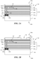
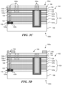
- FIGS 2A-2N are schematic cross-sectional views of a portion of a semiconductor substrate 106 undergoing a process for forming several embodiments of the semiconductor dies 102 shown in Figure 1 in accordance with embodiments of the technology.
- similar processing operations may utilize generally similar processing techniques.
- suitable techniques for performing the processing operations e.g., patterning a deposited material, removing portions of dielectric materials, depositing a conductive material, etc. are described only once for brevity.
- the process can include forming an integrated circuit 118 in and/or on the first side 106a of the semiconductor substrate 106.
- the integrated circuit 118 is shown schematically as a field-effect transistor having a source 120a, a drain 120b, and a gate 122 for illustration purposes.
- the integrated circuit 118 can also include vertical transistors, three-dimensional transistors, capacitors, and/or other suitable electrical components forming a dynamic random access memory (DRAM) and/or other suitable electronic devices.
- DRAM dynamic random access memory
- the process can include forming an insulator 124 on the semiconductor substrate 106.
- the insulator 124 includes four layers of silicon oxide, silicon nitride, and/or other suitable dielectrics (identified individually as first to fourth insulation materials 124a-124d, respectively).
- the insulator 124 can also include another desired number of dielectric and/or other suitable insulation materials.
- Techniques for forming the insulator 124 can include thermal oxidation, chemical vapor deposition ("CVD"), atomic layer deposition (“ALD”), spin-on glass, and/or other suitable techniques.
- the process can also include forming a conductive link 126 in the insulator 124 that is electrically connected to the integrated circuit 118.
- forming the conductive link 126 includes patterning the insulator 124 with photolithography and/or other suitable techniques, and removing a portion of the patterned insulator 124 to form an aperture 127 via wet etching, dry etching, reactive ion etching, and/or other suitable techniques.
- the aperture 127 may then be filled with a conductive material 129 (e.g., copper, aluminum, gold, and/or other suitable conductive materials) via physical vapor deposition (PVD), CVD, ALD, electroplating, and/or other suitable techniques.
- PVD physical vapor deposition
- CVD chemical vapor deposition
- ALD electroplating
- the process can include forming the first metallization layer 128a by forming a first dielectric 130 on the insulator 124, patterning the first dielectric 130 according to a desired metal routing profile, removing a portion of the first dielectric 130 to form trenches, channels, and/or other openings 135 in the first dielectric 130, and depositing a conductive material 137 (e.g., copper, aluminum, gold, and/or other suitable conductive materials) in the openings 135.
- the process can then include forming a first barrier 132 (e.g., BLOK provided by Applied Materials, Inc., Santa Clara, California) on the first metallization layer 128a and depositing a second dielectric 134 (e.g., silicon oxide) on the first barrier 132.
- the second dielectric 134 includes a first surface 134a proximate to the first barrier 132 and a second surface 134b opposite the first surface 134a.
- FIGS 2B-2H illustrate a through-substrate interconnect formation process module (hereinafter referred to as the "TSV module”) for forming a through-substrate interconnect 110 ( Figure 1 ) in the semiconductor substrate 106.
- the TSV module can include depositing a first photoresist 136 on the second dielectric 134 via spin coating and/or other suitable techniques. The first photoresist 136 can then be patterned to form a first opening 138.
- the term "photoresist” generally refers to a material that can be chemically modified when exposed to electromagnetic radiation. The term encompasses both positive photoresist that is configured to be soluble when activated by the electromagnetic radiation and negative photoresist that is configured to be insoluble when activated by light.
- the TSV module can include forming an interconnect aperture 140 in the semiconductor substrate 106.
- the interconnect aperture 140 can be formed by removing material from the first dielectric 130, the first barrier 132, the second dielectric 134, the insulator 124, and at least a portion of the semiconductor substrate 106 via the opening 138 in a continuous operation.
- forming the interconnect aperture 140 can include a first material removal operation (e.g., using wet etching) to remove a portion of the first dielectric 130, the first barrier 132, the second dielectric 134, and the insulator 124, and a second material removal operation (e.g., using reactive ion etching) to remove a portion of the semiconductor substrate 106.
- the TSV module can further include removing the first photoresist 136 and sequentially forming an aperture insulator 142, an aperture barrier 144, and a seed material 146 in the interconnect aperture 140.
- the aperture insulator 142 can include silicon oxide, silicon nitride, and/or other suitable insulation materials formed via thermal oxidation, CVD, ALD, and/or other suitable techniques.
- the aperture barrier 144 can include tantalum (Ta), tungsten (W), titanium nitride (TiN), and/or other suitable barrier materials formed via pulsed chemical vapor deposition ("pCVD"), ionic physical vapor deposition ("iPVD”), ALD, and/or other suitable techniques.
- the seed material 144 can include copper, tungsten, and/or other suitable conductive materials deposited via pCVD, iPVD, ALD, and/or other suitable techniques.
- the TSV module can also include depositing a second photoresist 148 on the seed material 146.
- the second photoresist 148 can then be patterned to form a second opening 150.
- the TSV module can include filling the interconnect aperture 140 with a first conductive material 152 via the second opening 150 to form the through-substrate interconnect 110.
- the first conductive material 152 includes a first portion 152a in the interconnect aperture 140 and a second portion 152b extending beyond the second dielectric 134.
- the first conductive material 152 can include copper, aluminum, tungsten, gold, and/or alloys of the foregoing constituents.
- the first conductive material 152 includes electrolytic copper introduced into the interconnect aperture 140.
- the electrolytic copper has an enhanced purity when compared to electrolessly disposed materials, and when compared to solder.
- the first conductive material 152 can be at least 90% copper and in some cases 99% copper.
- the second photoresist 148 may then be removed.
- the second portion 152b ( Figure 2F ) of the first conductive material 152 can be subsequently removed such that the first portion 152a of the first conductive material 152 is generally planar with the second surface 134b of the second dielectric 134.
- Techniques for removing the second portion 152b of the first conductive material 152 can include chemical-mechanical polishing ("CMP"), electrochemical-mechanical polishing (“ECMP”), and/or other suitable techniques.
- the TSV module can optionally include depositing a second barrier 154 (e.g., BLOK provided by Applied Materials, Inc., Santa Clara, California) on the second surface 134b of the second dielectric 134 and the first portion 152a of the first conductive material 152.
- depositing the second barrier 154 may be omitted.
- the TSV module discussed above includes depositing and patterning the second photoresist 148, in certain embodiments, the second photoresist 148 may be omitted. Instead, the TSV module can include depositing the first conductive material 152 with the first portion 152a in the interconnect aperture 140 and the second portion 152b substantially covering the second surface 134b of the second dielectric 134. Subsequently, at least a part of the second portion 152b may be removed to yield the through-substrate interconnect 110 as shown in Figure 2G .
- the process can include forming a second metallization layer.
- the process can include forming a third dielectric 156 on the optional second barrier 154.
- the third dielectric 156 includes a first surface 156a proximate to the optional second barrier 154 and a second surface 156b opposite the first surface 156a.
- a plurality of first vias 159 to the first metallization layer 128a may be formed through the third dielectric 156, the optional second barrier 154, and the second dielectric 134.
- the process can then include depositing a third photoresist 158 on the third dielectric 156 and patterning the third photoresist 158 to form third openings 160 corresponding to a desired routing profile for a second metallization layer 128b (not shown).
- the process can include removing a portion of the third dielectric 156 and optionally a portion of the second barrier 154 to form openings 162.
- the openings 162 expose at least a part of the second surface 134b of the second dielectric 134 and the upper surface of the first portion 152a of the first conductive material 152.
- the process can include filling the openings 162 and first vias 159 with a second conductive material 164 and subsequently removing excess second conductive material 164 external to the openings 162 such that the second conductive material 164 is generally planar with the second surface 156b of the third dielectric 156.
- the second conductive material 164 includes a first portion 164a, a second portion 164b extending laterally away from the first portion 164a, and a third portion 164c in the first vias 159.
- the first portion 164a of the second conductive material 164 is in direct physical contact with the first portion 152a of the first conductive material 152 of the through-substrate interconnect 110.
- the third portion 164c of the second conductive material 164 electrically connects the second portion 164b and the first metallization layer 128a.
- the second conductive material 164 includes the same composition (e.g., copper) as the first conductive material 152.
- the first and second conductive materials 152 and 164 may be generally homogeneous (a phantom line is used in Figure 2K to show an artificial demarcation between the first and second conductive materials 152 and 164).
- the second conductive material 164 may include a composition at least partially different than the first conductive material 152.
- the first metallization layer 128a is electrically connected to the through-substrate interconnect 110 via the second conductive material 164.
- the process can include forming additional metallization layers on the semiconductor substrate 106.
- Figures 2L and 2M illustrate operations of forming a third metallization layer 128c.
- the process can include depositing a fourth dielectric 166 on the second surface 156b of the third dielectric 156 and the second metallization layer 128b.
- the deposited fourth dielectric 166 has a first surface 166a proximate to the third dielectric 156 and a second surface 166b opposite the first surface 166a.
- the process can then include patterning and removing a portion of the fourth dielectric 166 to form a plurality of second vias 168 extending from the second surface 166b of the fourth dielectric 166 to the second metallization layer 128b.
- the third metallization layer 128c can then be formed following operations generally similar to those described with reference to Figures 2I and 2J .
- the third metallization layer 128c includes a third conductive material 170 electrically connected to the second metallization layer 128b via the second vias 168.
- the third conductive material 170 has the same composition (e.g., copper) as the first and second conductive materials 152 and 164.
- the third dielectric material 170 may have a composition different from the first and/or second dielectric materials 152 and 164.
- the process can also include processing the semiconductor substrate 106 to form additional features in and/or on the semiconductor substrate 106.
- a portion of the semiconductor substrate 106 can be removed from the second side 106b using a mechanical or chemical-mechanical technique to expose the through-substrate interconnect 110.
- a conductive component 172 e.g., a conductive pillar, a solder ball, a solder bump, a redistribution layer, a through-silicon via stud, and/or other suitable interconnect devices
- an external component not shown.
- first, second and third metallization layers 128a, 128b, and 128c are illustrated in Figures 2A-2M
- the process can include forming four, five, or any desired number of metallization layers by repeating at least some of the operations discussed above with reference to Figures 2L and 2M .
- the through-substrate interconnect 110 may be electrically connected to the second metallization layer 128b, the third metallization layer 128c, or the N-1 metallization layer (not shown).
- Several embodiments of the foregoing process can reduce the risk of damaging the electrical connection between the first metallization layer 128a and the conductive link 126.
- the inventors have observed that forming the through-substrate interconnect 110 before forming the first metallization layer 128a can result in a defective electrical connection between the first metallization layer 128a and the conductive link 126.
- several operations during the formation of the first metallization layer 128a e.g., deposition of the conductive material, removal of excess conductive material, etc.
- the risk of creating a defective electrical connection may be lowered.
- the selection of electrical connection between the through-substrate interconnect 110 and the metallization layers may be postponed until later processing stages than the via-first process.
- the number of generic intermediate products i.e., semiconductor dies with partially formed metallization layers
- the number of generic intermediate products may be increased to enable a production manager to continue producing the semiconductor dies 102 before making a decision concerning the final connection configuration of the semiconductor dies 102.
- FIGS 3A-3F are schematic cross-sectional views of a portion of a semiconductor substrate undergoing a process useful for forming several embodiments of the semiconductor dies 102 shown in Figure 1 in accordance with additional embodiments of the technology.
- the process can include forming the integrated circuit 118 in and/or on the semiconductor substrate 106, forming the conductive link 126, the first metallization layer 128a, and the first barrier 132 on the first metallization layer 128a, as discussed above with reference to Figure 2A .
- the process shown in Figure 3B can include utilizing the TSV module, as discussed above with reference to Figures 2B-2H , before depositing the second dielectric 134 on the first barrier 132. Subsequently, the second dielectric 134 may be formed on the first barrier 132 and the through-substrate interconnect 110. As a result, the through-substrate interconnect 110 may be generally planar with the first barrier 132 and may be in direct contact with the first surface 134a of the second dielectric 134.
- the process can include depositing the third dielectric 156 on the second dielectric 134.
- the first surface 156a of the third dielectric 156 can be in direct contact with the second surface 134b of the second dielectric 134.
- the process can include forming a plurality of access vias 180 in the second and third dielectrics 134 and 156 through the third dielectric 156, the second dielectric 134, and the barrier 132.
- the access vias 180 include (1) a first group 180a of access vias 180 that generally correspond to the through-substrate interconnect 110; and (2) a second group 180b of access vias 180 that generally correspond to the first metallization layer 128a.
- the process can then include depositing a photoresist 182 on the third dielectric 156 and patterning the photoresist 182 to form openings 184 corresponding to a desired routing profile for the second metallization layer 128b. As shown in Figure 3E , the process can include removing a portion of the third dielectric 156 to form openings 186. The openings 186 expose at least a part of the second surface 134b of the second dielectric 134 and are in communication with at least some of the access vias 180.
- the process can include filling the openings 186 and the access vias 180 with the second conductive material 164. Excess second conductive material 164 external to the openings 186 may then be removed such that the second conductive material 164 is generally planar with the second surface 156b of the third dielectric 156.
- the second conductive material 164 includes a first portion 164a, a second portion 164b extending laterally away from the first portion 164a, a third portion 164c in the first group 180a of the access vias 180, and a fourth portion 164d in the second group 180b of the access vias 180.
- the third portion 164c of the second conductive material 164 electrically connects the first portion 164a of the second conductive material 164 to the through-substrate interconnect 110.
- the fourth portion 164d of the second conductive material 164 electrically connects the second portion 164b of the second conductive material 164 to the first metallization layer 128a.
- the process can then include forming additional metallization layers and performing subsequent processing as discussed with reference to Figures 2L-2N .
- Figures 4A-4F are schematic cross-sectional views of a portion of a semiconductor substrate 100 undergoing a process useful for forming several embodiments of the semiconductor dies 102 shown in Figure 1 in accordance with yet additional embodiments of the technology.
- the process can include forming the integrated circuit 118 in and/or on the semiconductor substrate 106, forming the conductive link 126, the first metallization layer 128a, and the first barrier 132 on the first metallization layer 128a, as discussed above with reference to Figure 2A .
- the process can also include forming the second metallization layer 128b, as discussed above with reference to Figures 2H-2K .
- the process can then optionally include depositing the second barrier 154 on the second metallization layer 128b.
- the process can include forming the fourth dielectric 166 on the second barrier 154 and depositing a photoresist 190 on the fourth dielectric 166.
- the photoresist 190 can then be patterned to form openings 192 corresponding to a portion of the second metallization layer 128b and the through-substrate interconnect 110 (not shown).
- the exposed portion 194 a portion of the fourth dielectric 166 and the underlying second barrier 154 is exposed in the opening 192 (hereinafter referred to as the exposed portion 194).
- the process can include forming the interconnect aperture 140 in the semiconductor substrate 106 and removing the exposed portion 194 ( Figure 4B ).
- the interconnect aperture 140 may be formed and the exposed portion 194 may be removed in one continuous operation using a phase-shift mask, leaky-chrome mask, and/or other suitable techniques.
- the interconnect aperture 140 may be formed by etching with a first mask (not shown) generally corresponding to the interconnect aperture 140.
- the exposed portion 194 may be removed with a second mask (not shown) generally corresponding to the exposed portion 194.
- the exposed portion 194 may be removed via other suitable techniques.
- the process can include forming the aperture insulator 142 in the interconnect aperture 140.
- the aperture insulator 142 includes a first portion 142a in the interconnect aperture 140 and a second portion 142b external to the interconnect aperture 140.
- the second portion 142b at least partially overlaps and is in direct contact with the second metallization layer 128b.
- the aperture insulator 142 may only include the first portion 142a by using, for example, a photomask generally corresponding to the interconnect aperture 140 that was used when forming the aperture insulator 142.
- the process can include at least partially removing the second portion 142b of the aperture insulator 142 and exposing the second metallization layer 128b.
- the second portion 142b may be partially removed via a spacer etch. As a result, a part 142c of the second portion 142b remains on the second metallization layer 128b.
- the second portion 142b may be partially removed via laser ablation and/or other suitable techniques. In further embodiments, the second portion 142b may be completely removed.
- the process can then include depositing the aperture barrier 144 and the seed material 146 in the interconnect aperture 140, as discussed above with reference to Figures 2C . Then, the process can include filling the interconnect aperture 140 with the first conductive material 152, and removing excess first conductive material 152 from the fourth dielectric 166.
- the through-substrate interconnect 110 includes a vertical section 110a in the interconnect aperture 140 and a horizontal section 110b external to the interconnect aperture 140.
- the horizontal section 110b extends laterally toward the second metallization layer 128b such that at least a portion of the horizontal section 110b is in direct contact with a top surface of the second metallization layer 128b.
- the process can optionally include forming a third barrier 196 on the fourth dielectric 166 and the through-substrate interconnect 110.
- the process can then include forming additional metallization layers and performing subsequent processing as discussed with reference to Figures 2L-2N to yield the semiconductor die 102 shown in Figure 4E .
Landscapes
- Internal Circuitry In Semiconductor Integrated Circuit Devices (AREA)
- Chemical & Material Sciences (AREA)
- Chemical Kinetics & Catalysis (AREA)
- General Chemical & Material Sciences (AREA)
- Engineering & Computer Science (AREA)
- Manufacturing & Machinery (AREA)
Abstract
Description
- The present technology is directed generally to microelectronic devices with through-substrate interconnects and associated methods of manufacturing.
- Semiconductor dies typically include a plurality of integrated circuits, bond-pads coupled to the integrated circuits, and metal routing layers for routing electrical signals between the bond-pads and external contacts. Fabricating and packaging such semiconductor dies include forming interconnects to electrically couple the bond-pads and/or metal routing layers to externally devices (e.g., a lead frame, a printed circuit board, etc.).
- In some applications, the interconnects extend completely through or through a significant portion of the semiconductor dies (commonly referred to as "through-substrate interconnects"). One conventional process for forming through-substrate interconnects can include forming deep vias on the front and/or back side of a die in alignment with corresponding bond-pads. The vias are then filled with a conductive material (e.g., copper). Solder balls and/or other external electrical contacts are subsequently attached to the through-substrate interconnects.
- The through-substrate interconnects may be formed (1) prior to integrating processing (commonly referred to as a "via-first" process), or (2) after the integration processing has been substantially completed (commonly referred to as a "via-last" process). However, both the via-first and via-last processes have certain drawbacks, as discussed in more detail later. Accordingly, several improvements to the process of through-substrate formation may be desirable.
-
-
Figure 1 is a schematic cross-sectional view of a microelectronic package with stacked dies in accordance with embodiments of the technology. -
Figures 2A-2N are schematic cross-sectional views of a portion of a semiconductor substrate undergoing a process useful for forming several embodiments of the semiconductor dies shown inFigure 1 in accordance with embodiments of the technology. -
Figures 3A-3F are schematic cross-sectional views of a portion of a semiconductor substrate undergoing a process useful for forming several embodiments of the semiconductor dies shown inFigure 1 in accordance with additional embodiments of the technology. -
Figures 4A-4F are schematic cross-sectional views of a portion of a semiconductor substrate undergoing a process useful for forming several embodiments of the semiconductor dies shown inFigure 1 in accordance with yet additional embodiments of the technology. - Several embodiments of the present technology are described below with reference to processes for forming through vias and conductive routing layers in semiconductor substrates. Many details of certain embodiments are described below with reference to semiconductor dies. The term "semiconductor substrate" is used throughout to include a variety of articles of manufacture, including, for example, individual integrated circuit dies, imager dies, sensor dies, and/or dies having other semiconductor features.
- Several of the processes described below may be used to form through vias and conductive routing layers in an individual die or in a plurality of dies, on a wafer or portion of a wafer. The wafer or wafer portion (e.g., wafer form) can include an unsingulated wafer or wafer portion, or a repopulated carrier wafer. The repopulated carrier wafer can include an adhesive material (e.g., a flexible adhesive) surrounded by a generally rigid frame having a perimeter shape that is comparable to that of an unsingulated wafer and can include singulated elements (e.g., dies) surrounded by the adhesive.
- Many specific details of certain embodiments are set forth in
Figures 1-4F and the following text to provide a thorough understanding of these embodiments. Several other embodiments can have configurations, components, and/or processes different from those described below. A person skilled in the relevant art, therefore, will appreciate that additional embodiments may be practiced without several of the details of the embodiments shown inFigures 1-4F . -
Figure 1 is a schematic cross-sectional view of a portion of amicroelectronic package 100 in accordance with embodiments of the technology. As shown inFigure 1 , themicroelectronic package 100 can include a plurality of semiconductor dies 102 stacked in series with a plurality of conductive couplers 104 (e.g., solder balls). Four semiconductor dies 102 (identified individually as first, second, third, and fourth semiconductor dies 102a-102d, respectively) are shown inFigure 1 for illustration purposes. In other embodiments, themicroelectronic package 100 can include any other desired number of semiconductor dies 102 coupled to one another with wirebonds, solder balls, conductive tapes, and/or other suitable electrical connectors. - The
semiconductor dies 102 can individually include asemiconductor substrate 106 carrying asignal routing structure 108 proximate to afirst side 106a of thesemiconductor substrate 106, a plurality of bond-pads 112 (identified individually as first to fifth bond-pads 112a-112e, respectively) on thesignal routing structure 108, and a plurality of through-substrate interconnects 110 (identified individually as first tofourth interconnects 110a-110d, respectively) extending between thefirst side 106a and asecond side 106b of thesemiconductor substrate 106. Thesemiconductor dies 102 can also include an input/output ("I/O")buffer 114 associated with the first through-substrate interconnect 110a and a chip-select ("C/S")buffer 116 associated with the second, third, and fourth through-substrate interconnects 1 10b-l 10d. - The through-
substrate interconnects 110 can be selectively connected to certain metallization layers (not shown inFigure 1 ) in thesignal routing structures 108 for carrying electrical signals between the first andsecond sides signal routing structures 108 and the through-substrate interconnects 110 are discussed in more detail below with reference toFigures 2A-4F . - The
conductive couplers 104 can interface with corresponding bond-pads 112 based on a desired signal routing scheme. As shown inFigure 1 , not all of the bond-pads 112 are electrically coupled to one of theconductive couplers 104. For example, the first through-substrate interconnect 110a of thefirst semiconductor die 102a is electrically coupled via theconductive couplers 104 and the first bond-pad 112a of thefirst semiconductor die 102a. In contrast, the second bond-pad 112b of all the semiconductor dies 102, the third bond-pad 112c of the third semiconductor die 102c, and the third and fourth bond-pads fourth semiconductor die 102d are not electrically coupled to any of theconductive couplers 104. Instead, thesignal routing structure 108 routes a chip-select signal (and/or other suitable signals) received at the second bond-pad 112b of the first semiconductor die 102a to the C/S buffer 116 of the fourth semiconductor die 102d via the second through-substrate interconnect 110b of the first semiconductor die 102a, the third through-substrate interconnect 110c of thesecond semiconductor die 102b, and the fourth through-substrate interconnect 110d of the third semiconductor die 102c. - In operation, the electrically coupled first through-
substrate interconnect 110a of the semiconductor dies 102 forms an electrical path for carrying input/output signals to all the semiconductor dies 102. Thesignal routing structures 108 of the individual semiconductor dies 102 route the input/output signals to the individual I/O buffers 114 of the semiconductor dies 102 from the electrical path. Thesignal routing structure 108 can also route a chip-select signal (and/or other suitable signals) to aselected semiconductor die 102 to enable processing the input/output signals received at the I/O buffer 114 at aselected semiconductor die 102. For example, thesignal routing structure 108 routes a chip-select signal received at the fifth bond-pad 112e to the C/S buffer 116 of thefirst semiconductor die 102a to enable the first semiconductor die 102a to process the received input/output signals. In another example, thesignal routing structure 108 can also route a chip-select signal received at the fourth bond-pad 112d to thesecond semiconductor die 102b via the fourth through-substrate interconnect 110d of thefirst semiconductor die 102a. - In accordance with conventional techniques, the through-
substrate interconnects 110 may be formed based on a via-first process or a via-last process. However, the inventors have recognized that both the via-first and via-last processes have certain drawbacks. For example, the via-last process may not adequately accommodate routing the chip-select signals because such modification may significantly add cost and/or complexity to the manufacturing process. For example, techniques that may be used to route signals at the last metallization layer can include (1) controlling the formation (or the lack of formation) of conductive bumps to anadjacent semiconductor die 102; (2) routing the signals back down to the lower metallization layers; (3) adding control gates (e.g., MOSFET) to thesignal routing structure 108; (4) patterning each of the semiconductor dies 102 differently; and (5) adding a redistribution layer (not shown) on thesemiconductor dies 102. - The inventors also recognized that the via-first process may negatively impact the electrical reliability of the semiconductor dies 102 because the electrical contacts between the
signal routing structures 108 and integrated circuits (not shown) in thesemiconductor dies 102 may be damaged during formation of thesignal routing structures 108. Several embodiments of a process for addressing at least some of the foregoing drawbacks of the via-first and via-last processes are discussed below with reference toFigures 2A-2N . -
Figures 2A-2N are schematic cross-sectional views of a portion of asemiconductor substrate 106 undergoing a process for forming several embodiments of the semiconductor dies 102 shown inFigure 1 in accordance with embodiments of the technology. In the following description, similar processing operations may utilize generally similar processing techniques. As a result, suitable techniques for performing the processing operations (e.g., patterning a deposited material, removing portions of dielectric materials, depositing a conductive material, etc.) are described only once for brevity. - As shown in
Figure 2A , the process can include forming an integratedcircuit 118 in and/or on thefirst side 106a of thesemiconductor substrate 106. In the illustrated embodiment, theintegrated circuit 118 is shown schematically as a field-effect transistor having asource 120a, adrain 120b, and agate 122 for illustration purposes. In other embodiments, the integratedcircuit 118 can also include vertical transistors, three-dimensional transistors, capacitors, and/or other suitable electrical components forming a dynamic random access memory (DRAM) and/or other suitable electronic devices. - The process can include forming an
insulator 124 on thesemiconductor substrate 106. In the illustrated embodiment, theinsulator 124 includes four layers of silicon oxide, silicon nitride, and/or other suitable dielectrics (identified individually as first tofourth insulation materials 124a-124d, respectively). In other embodiments, theinsulator 124 can also include another desired number of dielectric and/or other suitable insulation materials. Techniques for forming theinsulator 124 can include thermal oxidation, chemical vapor deposition ("CVD"), atomic layer deposition ("ALD"), spin-on glass, and/or other suitable techniques. - The process can also include forming a
conductive link 126 in theinsulator 124 that is electrically connected to the integratedcircuit 118. In one embodiment, forming theconductive link 126 includes patterning theinsulator 124 with photolithography and/or other suitable techniques, and removing a portion of the patternedinsulator 124 to form anaperture 127 via wet etching, dry etching, reactive ion etching, and/or other suitable techniques. Theaperture 127 may then be filled with a conductive material 129 (e.g., copper, aluminum, gold, and/or other suitable conductive materials) via physical vapor deposition (PVD), CVD, ALD, electroplating, and/or other suitable techniques. In other embodiments, forming theconductive link 126 may include other processing operations in addition to or in lieu of the foregoing operations. - The process can include forming the
first metallization layer 128a by forming afirst dielectric 130 on theinsulator 124, patterning thefirst dielectric 130 according to a desired metal routing profile, removing a portion of thefirst dielectric 130 to form trenches, channels, and/or other openings 135 in thefirst dielectric 130, and depositing a conductive material 137 (e.g., copper, aluminum, gold, and/or other suitable conductive materials) in the openings 135. The process can then include forming a first barrier 132 (e.g., BLOK provided by Applied Materials, Inc., Santa Clara, California) on thefirst metallization layer 128a and depositing a second dielectric 134 (e.g., silicon oxide) on thefirst barrier 132. Thesecond dielectric 134 includes afirst surface 134a proximate to thefirst barrier 132 and asecond surface 134b opposite thefirst surface 134a. - After forming the
first metallization layer 128a,Figures 2B-2H illustrate a through-substrate interconnect formation process module (hereinafter referred to as the "TSV module") for forming a through-substrate interconnect 110 (Figure 1 ) in thesemiconductor substrate 106. As shown inFigure 2B , the TSV module can include depositing afirst photoresist 136 on thesecond dielectric 134 via spin coating and/or other suitable techniques. Thefirst photoresist 136 can then be patterned to form afirst opening 138. As used herein, the term "photoresist" generally refers to a material that can be chemically modified when exposed to electromagnetic radiation. The term encompasses both positive photoresist that is configured to be soluble when activated by the electromagnetic radiation and negative photoresist that is configured to be insoluble when activated by light. - As shown in
Figure 2C , the TSV module can include forming aninterconnect aperture 140 in thesemiconductor substrate 106. Theinterconnect aperture 140 can be formed by removing material from thefirst dielectric 130, thefirst barrier 132, thesecond dielectric 134, theinsulator 124, and at least a portion of thesemiconductor substrate 106 via theopening 138 in a continuous operation. In other embodiments, forming theinterconnect aperture 140 can include a first material removal operation (e.g., using wet etching) to remove a portion of thefirst dielectric 130, thefirst barrier 132, thesecond dielectric 134, and theinsulator 124, and a second material removal operation (e.g., using reactive ion etching) to remove a portion of thesemiconductor substrate 106. - As shown in
Figure 2D , the TSV module can further include removing thefirst photoresist 136 and sequentially forming anaperture insulator 142, anaperture barrier 144, and aseed material 146 in theinterconnect aperture 140. Theaperture insulator 142 can include silicon oxide, silicon nitride, and/or other suitable insulation materials formed via thermal oxidation, CVD, ALD, and/or other suitable techniques. Theaperture barrier 144 can include tantalum (Ta), tungsten (W), titanium nitride (TiN), and/or other suitable barrier materials formed via pulsed chemical vapor deposition ("pCVD"), ionic physical vapor deposition ("iPVD"), ALD, and/or other suitable techniques. Theseed material 144 can include copper, tungsten, and/or other suitable conductive materials deposited via pCVD, iPVD, ALD, and/or other suitable techniques. - As shown in
Figure 2E , the TSV module can also include depositing asecond photoresist 148 on theseed material 146. Thesecond photoresist 148 can then be patterned to form asecond opening 150. As shown inFigure 2F , the TSV module can include filling theinterconnect aperture 140 with a firstconductive material 152 via thesecond opening 150 to form the through-substrate interconnect 110. The firstconductive material 152 includes afirst portion 152a in theinterconnect aperture 140 and asecond portion 152b extending beyond thesecond dielectric 134. The firstconductive material 152 can include copper, aluminum, tungsten, gold, and/or alloys of the foregoing constituents. In particular embodiments, the firstconductive material 152 includes electrolytic copper introduced into theinterconnect aperture 140. The electrolytic copper has an enhanced purity when compared to electrolessly disposed materials, and when compared to solder. For example, the firstconductive material 152 can be at least 90% copper and in some cases 99% copper. Thesecond photoresist 148 may then be removed. - As shown in
Figure 2G , thesecond portion 152b (Figure 2F ) of the firstconductive material 152 can be subsequently removed such that thefirst portion 152a of the firstconductive material 152 is generally planar with thesecond surface 134b of thesecond dielectric 134. Techniques for removing thesecond portion 152b of the firstconductive material 152 can include chemical-mechanical polishing ("CMP"), electrochemical-mechanical polishing ("ECMP"), and/or other suitable techniques. As shown inFigure 2H , the TSV module can optionally include depositing a second barrier 154 (e.g., BLOK provided by Applied Materials, Inc., Santa Clara, California) on thesecond surface 134b of thesecond dielectric 134 and thefirst portion 152a of the firstconductive material 152. In other embodiments, depositing thesecond barrier 154 may be omitted. - Even though the TSV module discussed above includes depositing and patterning the
second photoresist 148, in certain embodiments, thesecond photoresist 148 may be omitted. Instead, the TSV module can include depositing the firstconductive material 152 with thefirst portion 152a in theinterconnect aperture 140 and thesecond portion 152b substantially covering thesecond surface 134b of thesecond dielectric 134. Subsequently, at least a part of thesecond portion 152b may be removed to yield the through-substrate interconnect 110 as shown inFigure 2G . - Following the TSV module, the process can include forming a second metallization layer. As shown in
Figure 2I , the process can include forming athird dielectric 156 on the optionalsecond barrier 154. Thethird dielectric 156 includes afirst surface 156a proximate to the optionalsecond barrier 154 and asecond surface 156b opposite thefirst surface 156a. Then, a plurality offirst vias 159 to thefirst metallization layer 128a may be formed through thethird dielectric 156, the optionalsecond barrier 154, and thesecond dielectric 134. - The process can then include depositing a
third photoresist 158 on thethird dielectric 156 and patterning thethird photoresist 158 to formthird openings 160 corresponding to a desired routing profile for asecond metallization layer 128b (not shown). As shown inFigure 2J , the process can include removing a portion of thethird dielectric 156 and optionally a portion of thesecond barrier 154 to formopenings 162. Theopenings 162 expose at least a part of thesecond surface 134b of thesecond dielectric 134 and the upper surface of thefirst portion 152a of the firstconductive material 152. - As shown in
Figure 2K , the process can include filling theopenings 162 andfirst vias 159 with a secondconductive material 164 and subsequently removing excess secondconductive material 164 external to theopenings 162 such that the secondconductive material 164 is generally planar with thesecond surface 156b of thethird dielectric 156. In the illustrated embodiment, the secondconductive material 164 includes afirst portion 164a, asecond portion 164b extending laterally away from thefirst portion 164a, and athird portion 164c in thefirst vias 159. Thefirst portion 164a of the secondconductive material 164 is in direct physical contact with thefirst portion 152a of the firstconductive material 152 of the through-substrate interconnect 110. Thethird portion 164c of the secondconductive material 164 electrically connects thesecond portion 164b and thefirst metallization layer 128a. - In one embodiment, the second
conductive material 164 includes the same composition (e.g., copper) as the firstconductive material 152. As a result, the first and secondconductive materials Figure 2K to show an artificial demarcation between the first and secondconductive materials 152 and 164). In other embodiments, the secondconductive material 164 may include a composition at least partially different than the firstconductive material 152. As a result, thefirst metallization layer 128a is electrically connected to the through-substrate interconnect 110 via the secondconductive material 164. - After forming the
second metallization layer 128b, the process can include forming additional metallization layers on thesemiconductor substrate 106. For example,Figures 2L and2M illustrate operations of forming athird metallization layer 128c. As shown inFigure 2L , the process can include depositing afourth dielectric 166 on thesecond surface 156b of thethird dielectric 156 and thesecond metallization layer 128b. The depositedfourth dielectric 166 has afirst surface 166a proximate to thethird dielectric 156 and asecond surface 166b opposite thefirst surface 166a. The process can then include patterning and removing a portion of thefourth dielectric 166 to form a plurality ofsecond vias 168 extending from thesecond surface 166b of thefourth dielectric 166 to thesecond metallization layer 128b. - The
third metallization layer 128c can then be formed following operations generally similar to those described with reference toFigures 2I and 2J . As shown inFigure 2M , thethird metallization layer 128c includes a thirdconductive material 170 electrically connected to thesecond metallization layer 128b via thesecond vias 168. In the illustrated embodiment, the thirdconductive material 170 has the same composition (e.g., copper) as the first and secondconductive materials dielectric material 170 may have a composition different from the first and/or seconddielectric materials - In certain embodiments, the process can also include processing the
semiconductor substrate 106 to form additional features in and/or on thesemiconductor substrate 106. For example, as shown inFigure 2N , a portion of thesemiconductor substrate 106 can be removed from thesecond side 106b using a mechanical or chemical-mechanical technique to expose the through-substrate interconnect 110. A conductive component 172 (e.g., a conductive pillar, a solder ball, a solder bump, a redistribution layer, a through-silicon via stud, and/or other suitable interconnect devices) can then be attached to the through-substrate interconnect 110 for interconnecting with an external component (not shown). - Even though only first, second and
third metallization layers Figures 2A-2M , in certain embodiments, the process can include forming four, five, or any desired number of metallization layers by repeating at least some of the operations discussed above with reference toFigures 2L and2M . In these embodiments, the through-substrate interconnect 110 may be electrically connected to thesecond metallization layer 128b, thethird metallization layer 128c, or the N-1 metallization layer (not shown). - Several embodiments of the foregoing process can reduce the risk of damaging the electrical connection between the
first metallization layer 128a and theconductive link 126. The inventors have observed that forming the through-substrate interconnect 110 before forming thefirst metallization layer 128a can result in a defective electrical connection between thefirst metallization layer 128a and theconductive link 126. Without being bound by theory, it is believed that several operations during the formation of thefirst metallization layer 128a (e.g., deposition of the conductive material, removal of excess conductive material, etc.) may physically weaken and/or damage the electrical connection between thefirst metallization layer 128a and theconductive link 126. As a result, by forming the through-substrate interconnect 110 subsequent to forming thefirst metallization layer 128a, the risk of creating a defective electrical connection may be lowered. - Several embodiments of the foregoing process can also be more cost-effective and flexible when compared to conventional techniques. For example, the selection of electrical connection between the through-
substrate interconnect 110 and the metallization layers may be postponed until later processing stages than the via-first process. As a result, the number of generic intermediate products (i.e., semiconductor dies with partially formed metallization layers) may be increased to enable a production manager to continue producing the semiconductor dies 102 before making a decision concerning the final connection configuration of the semiconductor dies 102. - Even though specific operations are discussed above with reference to
Figures 2A-2N for forming and connecting thesecond metallization layer 128b to the through-substrate interconnect 110, in other embodiments, thesecond metallization layer 128b may be formed and connected to the through-substrate interconnect 110 with additional and/or different process operations. For example,Figures 3A-3F are schematic cross-sectional views of a portion of a semiconductor substrate undergoing a process useful for forming several embodiments of the semiconductor dies 102 shown inFigure 1 in accordance with additional embodiments of the technology. As shown inFigure 3A , the process can include forming theintegrated circuit 118 in and/or on thesemiconductor substrate 106, forming theconductive link 126, thefirst metallization layer 128a, and thefirst barrier 132 on thefirst metallization layer 128a, as discussed above with reference toFigure 2A . - Unlike the embodiment shown in
Figure 2A , the process shown inFigure 3B can include utilizing the TSV module, as discussed above with reference toFigures 2B-2H , before depositing thesecond dielectric 134 on thefirst barrier 132. Subsequently, thesecond dielectric 134 may be formed on thefirst barrier 132 and the through-substrate interconnect 110. As a result, the through-substrate interconnect 110 may be generally planar with thefirst barrier 132 and may be in direct contact with thefirst surface 134a of thesecond dielectric 134. - As shown in
Figure 3C , the process can include depositing thethird dielectric 156 on thesecond dielectric 134. As a result, thefirst surface 156a of thethird dielectric 156 can be in direct contact with thesecond surface 134b of thesecond dielectric 134. The process can include forming a plurality of access vias 180 in the second andthird dielectrics third dielectric 156, thesecond dielectric 134, and thebarrier 132. The access vias 180 include (1) afirst group 180a of access vias 180 that generally correspond to the through-substrate interconnect 110; and (2) asecond group 180b of access vias 180 that generally correspond to thefirst metallization layer 128a. - The process can then include depositing a
photoresist 182 on thethird dielectric 156 and patterning thephotoresist 182 to formopenings 184 corresponding to a desired routing profile for thesecond metallization layer 128b. As shown inFigure 3E , the process can include removing a portion of thethird dielectric 156 to formopenings 186. Theopenings 186 expose at least a part of thesecond surface 134b of thesecond dielectric 134 and are in communication with at least some of theaccess vias 180. - As shown in
Figure 3F , the process can include filling theopenings 186 and the access vias 180 with the secondconductive material 164. Excess secondconductive material 164 external to theopenings 186 may then be removed such that the secondconductive material 164 is generally planar with thesecond surface 156b of thethird dielectric 156. The secondconductive material 164 includes afirst portion 164a, asecond portion 164b extending laterally away from thefirst portion 164a, athird portion 164c in thefirst group 180a of the access vias 180, and afourth portion 164d in thesecond group 180b of theaccess vias 180. Thethird portion 164c of the secondconductive material 164 electrically connects thefirst portion 164a of the secondconductive material 164 to the through-substrate interconnect 110. Thefourth portion 164d of the secondconductive material 164 electrically connects thesecond portion 164b of the secondconductive material 164 to thefirst metallization layer 128a. The process can then include forming additional metallization layers and performing subsequent processing as discussed with reference toFigures 2L-2N . -
Figures 4A-4F are schematic cross-sectional views of a portion of asemiconductor substrate 100 undergoing a process useful for forming several embodiments of the semiconductor dies 102 shown inFigure 1 in accordance with yet additional embodiments of the technology. As shown inFigure 4A , the process can include forming theintegrated circuit 118 in and/or on thesemiconductor substrate 106, forming theconductive link 126, thefirst metallization layer 128a, and thefirst barrier 132 on thefirst metallization layer 128a, as discussed above with reference toFigure 2A . The process can also include forming thesecond metallization layer 128b, as discussed above with reference toFigures 2H-2K . The process can then optionally include depositing thesecond barrier 154 on thesecond metallization layer 128b. - As shown in
Figure 4B , the process can include forming thefourth dielectric 166 on thesecond barrier 154 and depositing aphotoresist 190 on thefourth dielectric 166. Thephotoresist 190 can then be patterned to formopenings 192 corresponding to a portion of thesecond metallization layer 128b and the through-substrate interconnect 110 (not shown). As a result, a portion of thefourth dielectric 166 and the underlyingsecond barrier 154 is exposed in the opening 192 (hereinafter referred to as the exposed portion 194). - As shown in
Figure 4C , the process can include forming theinterconnect aperture 140 in thesemiconductor substrate 106 and removing the exposed portion 194 (Figure 4B ). In one embodiment, theinterconnect aperture 140 may be formed and the exposedportion 194 may be removed in one continuous operation using a phase-shift mask, leaky-chrome mask, and/or other suitable techniques. In another embodiment, theinterconnect aperture 140 may be formed by etching with a first mask (not shown) generally corresponding to theinterconnect aperture 140. The exposedportion 194 may be removed with a second mask (not shown) generally corresponding to the exposedportion 194. In other embodiments, the exposedportion 194 may be removed via other suitable techniques. - As shown in
Figure 4D , the process can include forming theaperture insulator 142 in theinterconnect aperture 140. In the illustrated embodiment, theaperture insulator 142 includes afirst portion 142a in theinterconnect aperture 140 and asecond portion 142b external to theinterconnect aperture 140. Thesecond portion 142b at least partially overlaps and is in direct contact with thesecond metallization layer 128b. In other embodiments, theaperture insulator 142 may only include thefirst portion 142a by using, for example, a photomask generally corresponding to theinterconnect aperture 140 that was used when forming theaperture insulator 142. - As shown in
Figure 4E , the process can include at least partially removing thesecond portion 142b of theaperture insulator 142 and exposing thesecond metallization layer 128b. In one embodiment, thesecond portion 142b may be partially removed via a spacer etch. As a result, apart 142c of thesecond portion 142b remains on thesecond metallization layer 128b. In other embodiments, thesecond portion 142b may be partially removed via laser ablation and/or other suitable techniques. In further embodiments, thesecond portion 142b may be completely removed. - The process can then include depositing the
aperture barrier 144 and theseed material 146 in theinterconnect aperture 140, as discussed above with reference toFigures 2C . Then, the process can include filling theinterconnect aperture 140 with the firstconductive material 152, and removing excess firstconductive material 152 from thefourth dielectric 166. - As shown in
Figure 4F , the through-substrate interconnect 110 includes avertical section 110a in theinterconnect aperture 140 and ahorizontal section 110b external to theinterconnect aperture 140. Thehorizontal section 110b extends laterally toward thesecond metallization layer 128b such that at least a portion of thehorizontal section 110b is in direct contact with a top surface of thesecond metallization layer 128b. The process can optionally include forming athird barrier 196 on thefourth dielectric 166 and the through-substrate interconnect 110. The process can then include forming additional metallization layers and performing subsequent processing as discussed with reference toFigures 2L-2N to yield the semiconductor die 102 shown inFigure 4E . - From the foregoing, it will be appreciated that specific embodiments of the technology have been described herein for purposes of illustration, but that various modifications may be made without deviating from the technology. Many of the elements of one embodiment may be combined with other embodiments in addition to or in lieu of the elements of the other embodiments. Accordingly, the technology is not limited except as by the appended claims.
- The following is a non-exhaustive list of numbered embodiments which may be claimed:
- 1. A semiconductor device, comprising:
- a semiconductor substrate;
- first and second metallization layers, the second metallization layer being spaced apart from the semiconductor substrate with the first metallization layer therebetween; and
- a conductive interconnect extending at least partially through the semiconductor substrate;
- wherein the first metallization layer is in electrical contact with the conductive interconnect via the second metallization layer.
- 2. The semiconductor device of embodiment 1 wherein:
- the semiconductor substrate includes a first side and a second side;
- the second metallization layer includes a first portion generally corresponding to the conductive interconnect and a second portion extending laterally from the first portion; and
- the semiconductor device also includes:
- an insulation between the first side of the semiconductor substrate and the first metallization layer;
- an integrated circuit on or in the semiconductor substrate;
- a conductive link at least partially in the insulation, the conductive link being between the integrated circuit and the first metallization layer;
- a dielectric between the first and second metallization layers; and
- the dielectric includes a conductive via directly between the first metallization layer and the second portion of the second metallization layer;
- the conductive interconnect includes a first end and a second end, the first end of the conductive interconnect being in direct contact with the first portion of the second metallization layer; and
- a solder ball attached to the second end of the conductive interconnect at the second side of the semiconductor substrate.
- 3. The semiconductor device of embodiment 1 wherein:
- the semiconductor substrate includes a first side and a second side;
- the second metallization layer includes a first portion generally corresponding to the conductive interconnect and a second portion extending laterally from the first portion; and
- the semiconductor device also includes:
- an insulation between the first side of the semiconductor substrate and the first metallization layer;
- an integrated circuit on or in the semiconductor substrate;
- a conductive link at least partially in the insulation, the conductive link extending between the integrated circuit and the first metallization layer; and
- a dielectric between the first and second metallization layers;
- the conductive interconnect includes a first end and a second end opposite the first end;
- the dielectric includes a first conductive via and a second conductive via spaced apart from the first conductive via, the first conductive via being directly between the first metallization layer and the second portion of the second metallization layer, the second conductive via being directly between the first portion of the second metallization layer and the first end of the conductive interconnect; and
- a solder ball attached to the second end of the conductive interconnect at the second side of the semiconductor substrate.
- 4. The semiconductor device of embodiment 1 wherein:
- the semiconductor substrate includes a first side and a second side;
- the second metallization layer includes a first metallization surface opposite a second metallization surface; and
- the semiconductor device also includes:
- an insulation between the first side of the semiconductor substrate and the first metallization layer;
- an integrated circuit on or in the semiconductor substrate;
- a conductive link at least partially in the insulation, the conductive link being between the integrated circuit and the first metallization layer;
- a dielectric between the first and second metallization layers; and
- the dielectric includes a conductive via directly between the first metallization layer and the second metallization layer;
- the conductive interconnect includes:
- an aperture extending at least partially between the first and second sides of the semiconductor substrate;
- a first section of a conductive material in the aperture;
- a second section of the conductive material external to the aperture;
- the second section of the conductive material extending laterally on the first section; and
- the second section is in direct contact with at least a portion of the second metallization surface of the second metallization layer; and
- a solder ball attached to the second end of the conductive interconnect at the second side of the semiconductor substrate.
- 5. The semiconductor device of embodiment 1 wherein:
- the semiconductor device also includes a dielectric between the first and second metallization layers; and
- the conductive interconnect includes a first end and a second end, the first end of the conductive interconnect being generally planar with the second surface of the dielectric, the second end being opposite the first end.
- 6. The semiconductor device of embodiment 1 wherein:
- the semiconductor device also includes a dielectric between the first and second metallization layers; and
- the conductive interconnect includes a first end and a second end, the first end of the conductive interconnect being in direct contact with the second metallization layer, the second end being opposite the first end.
- 7. The semiconductor device of embodiment 1 wherein:
- the second metallization layer includes a first portion generally corresponding to the conductive interconnect and a second portion extending laterally from the first portion;
- the semiconductor device also includes a dielectric between the first and second metallization layers, the dielectric having a first surface in direct contact with the first metallization layer and a second surface in direct contact with the second portion of the second metallization layer; and
- the conductive interconnect includes a first end and a second end, the first end of the conductive interconnect being in direct contact with the first portion of the second metallization layer, the second end being opposite the first end.
- 8. The semiconductor device of embodiment 1 wherein:
- the first metallization layer includes a first metallization surface proximate to the semiconductor substrate and a second metallization surface opposite the first metallization surface; and
- the conductive interconnect includes a first end and a second end, the first end of the conductive interconnect being generally flush with the second metallization surface of the first metallization layer, the second end being opposite the first end.
- 9. The semiconductor device of embodiment 1 wherein:
- the semiconductor device also includes a dielectric between the first and second metallization layers, the dielectric having a first surface in direct contact with the first metallization layer and a second surface opposite the first surface, the second surface being in direct contact with the second metallization layer;
- the dielectric includes a first conductive via and a second conductive via spaced apart from the first conductive via;
- the first conductive via is directly between the first metallization layer and the second metallization layer; and
- the second conductive via is directly between the second metallization layer and the conductive interconnect.
- 10. The semiconductor device of embodiment 1 wherein the conductive interconnect includes:
- an aperture extending at least partially in the semiconductor substrate;
- a first section of a conductive material in the aperture;
- a second section of the conductive material external to the aperture; and
- the second section of the conductive material extending laterally from the aperture and is in direct contact with the second metallization layer.
- 11. A semiconductor device, comprising:
- a semiconductor substrate;
- a plurality of metal routing layers carried by the semiconductor substrate, the plurality of metal routing layers including 1, 2, ..., N (N is a positive integer greater than 3) metal routing layers; and
- a conductive interconnect extending at least partially through the semiconductor substrate, the conductive interconnect including an end proximate to the metal routing layers;
- wherein the end of the conductive interconnect extends beyond or is generally flush with at least the first metal routing layer.
- 12. The semiconductor device of embodiment 11 wherein the end of the conductive interconnect extends beyond or is generally flush with the N-2 metal routing layer.
- 13. The semiconductor device of embodiment 11 wherein:
- the end of the conductive interconnect extends beyond or is generally flush with the N-2 metal routing layer; and
- the N-1 metal routing layer electrically connects the N-2 metal routing layer to the conductive interconnect.
- 14. The semiconductor device of embodiment 11 wherein the end of the conductive interconnect is in direct contact with the N-1 metal routing layer.
- 15. The semiconductor device of embodiment 11, further comprising a conductive via between the end of the conductive interconnect and the N-1 metal routing layer.
- 16. The semiconductor device of embodiment 11 wherein the end of the conductive interconnect includes a first section and a second section extending laterally from the first section, the second section being in direct contact with the N-1 metal routing layer.
- 17. A method for fabricating a semiconductor device, comprising:
- forming a first metallization layer on a semiconductor substrate;
- forming an interconnect aperture at least partially in the semiconductor substrate after the first metallization layer is formed;
- filling the interconnect aperture with a conductive material; and
- forming a second metallization layer on the first metallization layer, the second metallization layer being in electrical contact with the conductive material in the interconnect aperture.
- 18. The method of embodiment 17 wherein:
- forming an interconnect aperture includes:
- depositing a first dielectric on the first metallization layer;
- patterning the first dielectric and forming an opening generally corresponding to the interconnect aperture; and
- etching the first dielectric and the semiconductor substrate via the opening;
- filling the interconnect aperture includes:
- introducing a first conductive material in the interconnect aperture; and
- removing excess first conductive material external to the interconnect aperture; and
- forming a second metallization layer includes:
- depositing a second dielectric on the first dielectric and the conductive material in the interconnect aperture;
- patterning the deposited second dielectric based on a desired profile of the second metallization layer; and
- forming a via and a depression in the patterned second dielectric, the via exposing at least a portion of the first metallization layer, the depression exposing at least a portion of the first conductive material in the interconnect aperture; and
- filling the via and the depression with a second conductive material, the second conductive material having a first portion in direct contact with the first conductive material in the interconnect aperture and a second portion in the via in direct contact with the first metallization layer.
- forming an interconnect aperture includes:
- 19. The method of embodiment 17 wherein:
- forming an interconnect aperture includes:
- patterning the semiconductor substrate with the first metallization layer and forming an opening generally corresponding to the interconnect aperture; and
- etching the semiconductor substrate via the opening;
- filling the interconnect aperture includes:
- introducing a first conductive material in the interconnect aperture; and
- removing excess first conductive material external to the interconnect aperture; and
- forming a second metallization layer includes:
- depositing a first dielectric on the first metallization layer and the first conductive material in the interconnect aperture;
- forming a first via and a second via in the first dielectric, the first via exposing at least a portion of the first metallization layer, the second via exposing at least a portion of the first conductive material in the interconnect aperture;
- depositing a second dielectric on the first dielectric;
- patterning the deposited second dielectric based on a desired profile of the second metallization layer;
- forming a depression in the patterned second dielectric, the depression generally corresponding the to desired profile of the second metallization layer; and filling the first and second vias and the depression with a second conductive material.
- forming an interconnect aperture includes:
- 20. The method of embodiment 17 wherein:
- forming a second metallization layer includes:
- depositing a first dielectric on the first metallization layer;
- patterning the first dielectric based on a desired profile of the second metallization layer;
- forming a via and a depression in the first dielectric, the depression generally corresponding to the desired profile of the second metallization layer; and
- filling the via and the depression with a first conductive material; and forming an interconnect aperture includes:
- depositing a second dielectric on the second metallization layer and the first dielectric;
- patterning the second dielectric and forming an opening generally corresponding to the interconnect aperture and at least a portion of the second metallization layer;
- etching the first and second dielectrics and the semiconductor substrate via the opening;
- depositing an insulation material in the interconnect aperture and on the second metallization layer;
- removing at least a portion of the insulation material on the second metallization layer; and
- filling the interconnect aperture with a second conductive material via the opening, at least a portion of the second conductive material being in direct contact with the second metallization layer.
- forming a second metallization layer includes:
- 21. The method of embodiment 17 wherein:
- the conductive material is a first conductive material; and
- forming a second metallization layer includes:
- depositing a dielectric on the conductive material in the interconnect aperture;
- forming a depression in the dielectric, the depression exposing at least a portion of the conductive material in the interconnect aperture; and
- filling the depression with a second conductive material, the second conductive material having a first portion in direct contact with the first conductive material in the interconnect aperture and a second portion extending laterally from the first portion.
- 22. The method of embodiment 17 wherein:
- the conductive material is a first conductive material; and
- forming a second metallization layer includes:
- depositing a dielectric on the first metallization layer and the first conductive material in the interconnect aperture;
- forming a first via and a second via in the dielectric, the first via exposing at least a portion of the first metallization layer, the second via exposing at least a portion of the first conductive material in the interconnect aperture; and filling the first and second vias with a second conductive material.
- 23. The method of embodiment 17 wherein:
- the conductive material is a first conductive material; and
- forming an interconnect aperture includes:
- depositing a dielectric on the second metallization layer;
- forming the interconnect aperture through the dielectric and the semiconductor substrate;
- exposing at least a portion of the second metallization layer; and
- depositing a second conductive material in the interconnect aperture and onto the exposed portion of the second conductive material.
- 24. A method for fabricating a semiconductor device, comprising:
- forming a first, second, ..., and Nth metallization layers on a semiconductor substrate, N being a positive integer not less than 3;
- forming an interconnect aperture at least partially in the semiconductor substrate at least after the first metallization layer is formed; and
- filling the interconnect aperture with a conductive material, the conductive material being in electrical contact with at least one of the metallization layers.
- 25. The method of embodiment 24 wherein forming an interconnect aperture includes forming the interconnect aperture at least partially in the semiconductor substrate after the N-2 metallization layer is formed.
- 26. The method of embodiment 24 wherein:
- forming an interconnect aperture includes forming the interconnect aperture at least partially in the semiconductor substrate after the N-2 metallization layer is formed; and
- forming a first, second, ..., and Nth metallization layers includes forming the N-1 metallization layer after filling the interconnect aperture with the conductive material.
- 27. The method of embodiment 24 wherein:
- forming an interconnect aperture includes forming the interconnect aperture at least partially in the semiconductor substrate after the N-2 metallization layer is formed;
- forming a first, second, ..., and Nth metallization layers includes forming the N-1 metallization layer after filling the interconnect aperture with the conductive material; and
- the method further includes directly contacting the N-1 metallization layer with the conductive material in the interconnect aperture.
- 28. The method of embodiment 24 wherein:
- forming an interconnect aperture includes forming the interconnect aperture at least partially in the semiconductor substrate after the N-2 metallization layer is formed;
- forming a first, second, ..., and Nth metallization layers includes forming the N-1 metallization layer after filling the interconnect aperture with the conductive material; and
- the method further includes forming a conductive via directly between the N-1 metallization layer and the conductive material in the interconnect aperture.
- 29. The method of embodiment 24 wherein:
- forming an interconnect aperture includes forming the interconnect aperture at least partially in the semiconductor substrate after the N-1 metallization layer is formed; and
- filling the interconnect aperture includes filling the interconnect aperture with the conductive material with a first portion in direct contact with the N-1 metallization layer and a second portion in the interconnect aperture.
- 30. The method of embodiment 24 wherein:
- forming an interconnect aperture includes forming the interconnect aperture at least partially in the semiconductor substrate after the N-1 metallization layer is formed;
- the method further includes exposing at least a portion of the N-1 metallization layer; and
- filling the interconnect aperture includes introducing the interconnect aperture into the interconnect aperture and onto the exposed portion of the N-1 metallization layer.
Claims (15)
- A method for fabricating a semiconductor device, comprising:forming a first, second, ..., Nth metallization layers on a semiconductor substrate, N being a positive integer not less than 3;forming an interconnect aperture at least partially in the semiconductor substrate; andfilling the interconnect aperture with a conductive material, the conductive material being in electrical contact with at least one of the metallization layers.
- The method of claim 1, wherein forming the first, second, ..., Nth metallization layers comprises:
forming an N-2 metallization layer on the semiconductor substrate. - The method of claim 2, further comprising:
depositing a first dielectric layer over the N-2 metallization layer and the interconnect aperture. - The method of claim 3, wherein forming the interconnect aperture comprises:
forming the interconnect aperture at least partially in the semiconductor substrate after the N-2 metallization layer is formed. - The method of claim 4, wherein forming the first, second, ..., Nth metallization layers comprises:
forming an N-1 metallization layer after filling the interconnect aperture with the conductive material. - The method of claim 5, wherein the N-1 metallization layer includes a second conductive material having a first portion in direct contact with the conductive material in the interconnect aperture, a second portion continuous with the first portion and extending laterally away from the first portion, and a third portion continuous with the second portion.
- The method of claim 6, further comprising:
filling at least one via between the N-1 metallization layer and the N-2 metallization layer. - The method of claim 5, wherein the N-1 metallization layer is in direct contact with the conductive material in the interconnect aperture.
- The method of claim 5, further comprising:
forming a conductive via directly between the N-1 metallization layer and the conductive material in the interconnect aperture. - The method of claim 4, wherein filling the interconnect aperture comprises:
filling the interconnect aperture with the conductive material with a first portion in direct contact with an N-1 metallization layer and a second portion in the interconnect aperture. - The method of claim 4, further comprising:
exposing at least a portion of an N-1 metallization layer. - The method of claim 11, wherein filling the interconnect aperture comprises:
introducing the conductive material into the interconnect aperture and onto the exposed portion of the N-1 metallization layer. - A semiconductor device, comprising:a semiconductor substrate;a plurality of metal routing layers carried by the semiconductor substrate, the plurality of metal routing layers including 1, 2, ..., N (N is a positive integer greater than 3) metal routing layers; anda conductive interconnect extending at least partially through the semiconductor substrate, the conductive interconnect including an end proximate to the plurality of metal routing layers, wherein the end of the conductive interconnect extends beyond or is generally flush with at least one metal routing layer of the plurality of metal routing layers.
- The semiconductor device of claim 13, wherein the end of the conductive interconnect extends beyond or is generally flush with an N-2 metal routing layer.
- The semiconductor device of claim 13, wherein the end of the conductive interconnect is in direct contact with an N-1 metal routing layer.
Applications Claiming Priority (3)
| Application Number | Priority Date | Filing Date | Title |
|---|---|---|---|
| US12/701,800 US8907457B2 (en) | 2010-02-08 | 2010-02-08 | Microelectronic devices with through-substrate interconnects and associated methods of manufacturing |
| EP11740230.5A EP2534682B1 (en) | 2010-02-08 | 2011-01-31 | Microelectronic devices with through-substrate interconnects and associated methods of manufacturing |
| PCT/US2011/023150 WO2011097165A2 (en) | 2010-02-08 | 2011-01-31 | Microelectronic devices with through-substrate interconnects and associated methods of manufacturing |
Related Parent Applications (1)
| Application Number | Title | Priority Date | Filing Date |
|---|---|---|---|
| EP11740230.5A Division EP2534682B1 (en) | 2010-02-08 | 2011-01-31 | Microelectronic devices with through-substrate interconnects and associated methods of manufacturing |
Publications (2)
| Publication Number | Publication Date |
|---|---|
| EP4322215A2 true EP4322215A2 (en) | 2024-02-14 |
| EP4322215A3 EP4322215A3 (en) | 2024-07-03 |
Family
ID=44353051
Family Applications (2)
| Application Number | Title | Priority Date | Filing Date |
|---|---|---|---|
| EP11740230.5A Active EP2534682B1 (en) | 2010-02-08 | 2011-01-31 | Microelectronic devices with through-substrate interconnects and associated methods of manufacturing |
| EP23199195.1A Pending EP4322215A3 (en) | 2010-02-08 | 2011-01-31 | Microelectronic devices with through-substrate interconnects and associated methods of manufacturing |
Family Applications Before (1)
| Application Number | Title | Priority Date | Filing Date |
|---|---|---|---|
| EP11740230.5A Active EP2534682B1 (en) | 2010-02-08 | 2011-01-31 | Microelectronic devices with through-substrate interconnects and associated methods of manufacturing |
Country Status (7)
| Country | Link |
|---|---|
| US (5) | US8907457B2 (en) |
| EP (2) | EP2534682B1 (en) |
| KR (1) | KR101441776B1 (en) |
| CN (1) | CN102804370B (en) |
| SG (3) | SG183204A1 (en) |
| TW (1) | TWI474459B (en) |
| WO (1) | WO2011097165A2 (en) |
Families Citing this family (45)
| Publication number | Priority date | Publication date | Assignee | Title |
|---|---|---|---|---|
| US7968460B2 (en) | 2008-06-19 | 2011-06-28 | Micron Technology, Inc. | Semiconductor with through-substrate interconnect |
| US8907457B2 (en) | 2010-02-08 | 2014-12-09 | Micron Technology, Inc. | Microelectronic devices with through-substrate interconnects and associated methods of manufacturing |
| US8786066B2 (en) * | 2010-09-24 | 2014-07-22 | Intel Corporation | Die-stacking using through-silicon vias on bumpless build-up layer substrates including embedded-dice, and processes of forming same |
| WO2012061633A2 (en) | 2010-11-03 | 2012-05-10 | Netlist, Inc. | Method and apparatus for optimizing driver load in a memory package |
| US8513817B2 (en) | 2011-07-12 | 2013-08-20 | Invensas Corporation | Memory module in a package |
| US8823165B2 (en) | 2011-07-12 | 2014-09-02 | Invensas Corporation | Memory module in a package |
| US8502390B2 (en) | 2011-07-12 | 2013-08-06 | Tessera, Inc. | De-skewed multi-die packages |
| US8659143B2 (en) | 2011-10-03 | 2014-02-25 | Invensas Corporation | Stub minimization for wirebond assemblies without windows |
| US8441111B2 (en) | 2011-10-03 | 2013-05-14 | Invensas Corporation | Stub minimization for multi-die wirebond assemblies with parallel windows |
| US8610260B2 (en) | 2011-10-03 | 2013-12-17 | Invensas Corporation | Stub minimization for assemblies without wirebonds to package substrate |
| US8345441B1 (en) | 2011-10-03 | 2013-01-01 | Invensas Corporation | Stub minimization for multi-die wirebond assemblies with parallel windows |
| EP2769409A1 (en) | 2011-10-03 | 2014-08-27 | Invensas Corporation | Stub minimization for multi-die wirebond assemblies with orthogonal windows |
| US8436477B2 (en) | 2011-10-03 | 2013-05-07 | Invensas Corporation | Stub minimization using duplicate sets of signal terminals in assemblies without wirebonds to package substrate |
| US8436457B2 (en) * | 2011-10-03 | 2013-05-07 | Invensas Corporation | Stub minimization for multi-die wirebond assemblies with parallel windows |
| JP5887414B2 (en) | 2011-10-03 | 2016-03-16 | インヴェンサス・コーポレイション | Stub minimization of multi-die wirebond assemblies with parallel windows |
| JP2014528652A (en) | 2011-10-03 | 2014-10-27 | インヴェンサス・コーポレイション | Stub minimization by offsetting the terminal grid from the center of the package |
| US8659141B2 (en) | 2011-10-03 | 2014-02-25 | Invensas Corporation | Stub minimization using duplicate sets of terminals for wirebond assemblies without windows |
| US9673132B2 (en) | 2012-04-27 | 2017-06-06 | Taiwan Semiconductor Manufacting Company, Ltd. | Interconnection structure with confinement layer |
| US8787034B2 (en) | 2012-08-27 | 2014-07-22 | Invensas Corporation | Co-support system and microelectronic assembly |
| US8848392B2 (en) | 2012-08-27 | 2014-09-30 | Invensas Corporation | Co-support module and microelectronic assembly |
| US8848391B2 (en) | 2012-08-27 | 2014-09-30 | Invensas Corporation | Co-support component and microelectronic assembly |
| US9368477B2 (en) | 2012-08-27 | 2016-06-14 | Invensas Corporation | Co-support circuit panel and microelectronic packages |
| US10283854B2 (en) | 2012-10-08 | 2019-05-07 | Taoglas Group Holdings Limited | Low-cost ultra wideband LTE antenna |
| US9064850B2 (en) * | 2012-11-15 | 2015-06-23 | Taiwan Semiconductor Manufacturing Company, Ltd. | Through-substrate via formation with improved topography control |
| KR102041500B1 (en) | 2013-03-08 | 2019-11-06 | 삼성전자 주식회사 | Semiconductor package |
| US9070423B2 (en) | 2013-06-11 | 2015-06-30 | Invensas Corporation | Single package dual channel memory with co-support |
| US9123555B2 (en) | 2013-10-25 | 2015-09-01 | Invensas Corporation | Co-support for XFD packaging |
| US9865523B2 (en) | 2014-01-17 | 2018-01-09 | Taiwan Semiconductor Manufacturing Company, Ltd. | Robust through-silicon-via structure |
| US9520370B2 (en) | 2014-05-20 | 2016-12-13 | Micron Technology, Inc. | Methods of forming semiconductor device assemblies and interconnect structures, and related semiconductor device assemblies and interconnect structures |
| US9219053B1 (en) * | 2014-07-07 | 2015-12-22 | Macronix International Co., Ltd. | Three dimensional stacked multi-chip structure and manufacturing method of the same |
| US9281296B2 (en) | 2014-07-31 | 2016-03-08 | Invensas Corporation | Die stacking techniques in BGA memory package for small footprint CPU and memory motherboard design |
| US9691437B2 (en) | 2014-09-25 | 2017-06-27 | Invensas Corporation | Compact microelectronic assembly having reduced spacing between controller and memory packages |
| DE102014115105B4 (en) | 2014-10-09 | 2023-06-22 | Taiwan Semiconductor Manufacturing Company, Ltd. | Semiconductor device and method of manufacturing a semiconductor device |
| US9484080B1 (en) | 2015-11-09 | 2016-11-01 | Invensas Corporation | High-bandwidth memory application with controlled impedance loading |
| US9755310B2 (en) | 2015-11-20 | 2017-09-05 | Taoglas Limited | Ten-frequency band antenna |
| FR3046878B1 (en) * | 2016-01-19 | 2018-05-18 | Kobus Sas | METHOD FOR MANUFACTURING AN INTERCONNECTION COMPRISING A VIA EXTENDING THROUGH A SUBSTRATE |
| KR102497205B1 (en) | 2016-03-03 | 2023-02-09 | 삼성전자주식회사 | Semiconductor devices having through electrodes and methods for fabricating the same |
| US9679613B1 (en) | 2016-05-06 | 2017-06-13 | Invensas Corporation | TFD I/O partition for high-speed, high-density applications |
| CN112133691A (en) * | 2019-06-24 | 2020-12-25 | 台湾积体电路制造股份有限公司 | Semiconductor structure and method of making the same |
| US11658069B2 (en) * | 2020-03-26 | 2023-05-23 | Taiwan Semiconductor Manufacturing Co., Ltd. | Method for manufacturing a semiconductor device having an interconnect structure over a substrate |
| DE102020124131B4 (en) | 2020-03-26 | 2025-01-09 | Taiwan Semiconductor Manufacturing Co., Ltd. | SEMICONDUCTOR DEVICE AND METHOD |
| US11621219B2 (en) | 2021-02-18 | 2023-04-04 | Rockwell Collins, Inc. | Method and apparatus for through silicon die level interconnect |
| US20220270960A1 (en) | 2021-02-23 | 2022-08-25 | Texas Instruments Incorporated | Open-Cavity Package for Chip Sensor |
| KR20220153711A (en) * | 2021-05-11 | 2022-11-21 | 삼성전자주식회사 | Semiconductor device including through electrode and semiconductor package including the same |
| US12068363B2 (en) * | 2021-07-29 | 2024-08-20 | Taiwan Semiconductor Manufacturing Company, Ltd. | Structure formation in a semiconductor device |
Family Cites Families (62)
| Publication number | Priority date | Publication date | Assignee | Title |
|---|---|---|---|---|
| US5173442A (en) | 1990-07-23 | 1992-12-22 | Microelectronics And Computer Technology Corporation | Methods of forming channels and vias in insulating layers |
| US6620731B1 (en) | 1997-12-18 | 2003-09-16 | Micron Technology, Inc. | Method for fabricating semiconductor components and interconnects with contacts on opposing sides |
| JPH11251316A (en) * | 1998-03-02 | 1999-09-17 | Toshiba Corp | Method for manufacturing multi-chip semiconductor device |
| US7449098B1 (en) | 1999-10-05 | 2008-11-11 | Novellus Systems, Inc. | Method for planar electroplating |
| US6107186A (en) | 1999-01-27 | 2000-08-22 | Advanced Micro Devices, Inc. | High planarity high-density in-laid metallization patterns by damascene-CMP processing |
| US6221769B1 (en) | 1999-03-05 | 2001-04-24 | International Business Machines Corporation | Method for integrated circuit power and electrical connections via through-wafer interconnects |
| US6455425B1 (en) | 2000-01-18 | 2002-09-24 | Advanced Micro Devices, Inc. | Selective deposition process for passivating top interface of damascene-type Cu interconnect lines |
| US6524926B1 (en) | 2000-11-27 | 2003-02-25 | Lsi Logic Corporation | Metal-insulator-metal capacitor formed by damascene processes between metal interconnect layers and method of forming same |
| US6638688B2 (en) | 2000-11-30 | 2003-10-28 | Taiwan Semiconductor Manufacturing Co. Ltd. | Selective electroplating method employing annular edge ring cathode electrode contact |
| US20020163072A1 (en) * | 2001-05-01 | 2002-11-07 | Subhash Gupta | Method for bonding wafers to produce stacked integrated circuits |
| US6611052B2 (en) | 2001-11-16 | 2003-08-26 | Micron Technology, Inc. | Wafer level stackable semiconductor package |
| US6787460B2 (en) | 2002-01-14 | 2004-09-07 | Samsung Electronics Co., Ltd. | Methods of forming metal layers in integrated circuit devices using selective deposition on edges of recesses and conductive contacts so formed |
| US6642081B1 (en) | 2002-04-11 | 2003-11-04 | Robert Patti | Interlocking conductor method for bonding wafers to produce stacked integrated circuits |
| US6847077B2 (en) | 2002-06-25 | 2005-01-25 | Agere Systems, Inc. | Capacitor for a semiconductor device and method for fabrication therefor |
| US6800930B2 (en) | 2002-07-31 | 2004-10-05 | Micron Technology, Inc. | Semiconductor dice having back side redistribution layer accessed using through-silicon vias, and assemblies |
| JP3972846B2 (en) | 2003-03-25 | 2007-09-05 | セイコーエプソン株式会社 | Manufacturing method of semiconductor device |
| JP3891299B2 (en) | 2003-05-06 | 2007-03-14 | セイコーエプソン株式会社 | Semiconductor device manufacturing method, semiconductor device, semiconductor device, electronic device |
| JP4130158B2 (en) | 2003-06-09 | 2008-08-06 | 三洋電機株式会社 | Semiconductor device manufacturing method, semiconductor device |
| US7111149B2 (en) | 2003-07-07 | 2006-09-19 | Intel Corporation | Method and apparatus for generating a device ID for stacked devices |
| DE10331197B4 (en) | 2003-07-10 | 2012-09-06 | Deere & Company | Crop pickup device with conveyor belt assembly |
| US7364985B2 (en) | 2003-09-29 | 2008-04-29 | Micron Technology, Inc. | Method for creating electrical pathways for semiconductor device structures using laser machining processes |
| JP4340517B2 (en) * | 2003-10-30 | 2009-10-07 | Okiセミコンダクタ株式会社 | Semiconductor device and manufacturing method thereof |
| US7091124B2 (en) | 2003-11-13 | 2006-08-15 | Micron Technology, Inc. | Methods for forming vias in microelectronic devices, and methods for packaging microelectronic devices |
| KR101064288B1 (en) | 2004-01-09 | 2011-09-14 | 매그나칩 반도체 유한회사 | Contact hole formation method of semiconductor device |
| JPWO2005101476A1 (en) | 2004-04-16 | 2008-03-06 | 独立行政法人科学技術振興機構 | Semiconductor element and method of manufacturing semiconductor element |
| TWI245379B (en) | 2004-05-19 | 2005-12-11 | Sanyo Electric Co | Semiconductor device and method for manufacturing same |
| US7199050B2 (en) | 2004-08-24 | 2007-04-03 | Micron Technology, Inc. | Pass through via technology for use during the manufacture of a semiconductor device |
| US7575999B2 (en) | 2004-09-01 | 2009-08-18 | Micron Technology, Inc. | Method for creating conductive elements for semiconductor device structures using laser ablation processes and methods of fabricating semiconductor device assemblies |
| US20060246699A1 (en) | 2005-03-18 | 2006-11-02 | Weidman Timothy W | Process for electroless copper deposition on a ruthenium seed |
| FR2884645B1 (en) | 2005-04-19 | 2007-08-10 | St Microelectronics Sa | METHOD FOR PRODUCING AN INTEGRATED CIRCUIT COMPRISING A CAPACITOR |
| US7317256B2 (en) | 2005-06-01 | 2008-01-08 | Intel Corporation | Electronic packaging including die with through silicon via |
| US7488680B2 (en) | 2005-08-30 | 2009-02-10 | International Business Machines Corporation | Conductive through via process for electronic device carriers |
| FR2890783B1 (en) | 2005-09-12 | 2007-11-30 | St Microelectronics | INTEGRATED ELECTRONIC CIRCUIT INCORPORATING A CAPACITOR |
| JP2008066679A (en) | 2006-09-11 | 2008-03-21 | Manabu Bonshihara | Solid-state imaging device and manufacturing method thereof |
| US7863189B2 (en) * | 2007-01-05 | 2011-01-04 | International Business Machines Corporation | Methods for fabricating silicon carriers with conductive through-vias with low stress and low defect density |
| KR100850115B1 (en) * | 2007-05-18 | 2008-08-04 | 주식회사 동부하이텍 | Semiconductor Device Bonding Method |
| US8003517B2 (en) | 2007-05-29 | 2011-08-23 | Freescale Semiconductor, Inc. | Method for forming interconnects for 3-D applications |
| US7932175B2 (en) | 2007-05-29 | 2011-04-26 | Freescale Semiconductor, Inc. | Method to form a via |
| KR100895813B1 (en) | 2007-06-20 | 2009-05-06 | 주식회사 하이닉스반도체 | Manufacturing method of semiconductor package |
| KR100881199B1 (en) | 2007-07-02 | 2009-02-05 | 삼성전자주식회사 | Semiconductor device having through electrode and method of manufacturing same |
| KR100906065B1 (en) * | 2007-07-12 | 2009-07-03 | 주식회사 동부하이텍 | Semiconductor chip, manufacturing method thereof and laminated package having same |
| US7659595B2 (en) * | 2007-07-16 | 2010-02-09 | Taiwan Semiconductor Manufacturing Company, Ltd. | Embedded bonding pad for backside illuminated image sensor |
| US7973413B2 (en) * | 2007-08-24 | 2011-07-05 | Taiwan Semiconductor Manufacturing Company, Ltd. | Through-substrate via for semiconductor device |
| KR101448150B1 (en) | 2007-10-04 | 2014-10-08 | 삼성전자주식회사 | A multi-chip package memory in which memory chips are stacked, a method of stacking memory chips, and a method of controlling operations of a multi-chip package memory |
| KR101374338B1 (en) * | 2007-11-14 | 2014-03-14 | 삼성전자주식회사 | semicondoctor device having through-via and method of forming the same |
| KR101176187B1 (en) | 2007-11-21 | 2012-08-22 | 삼성전자주식회사 | Stacked semiconductor device and method for thereof serial path build up |
| JP2009147218A (en) * | 2007-12-17 | 2009-07-02 | Toshiba Corp | Semiconductor device and manufacturing method thereof |
| US7843064B2 (en) * | 2007-12-21 | 2010-11-30 | Taiwan Semiconductor Manufacturing Company, Ltd. | Structure and process for the formation of TSVs |
| KR101420817B1 (en) | 2008-01-15 | 2014-07-21 | 삼성전자주식회사 | Semiconductor integrated circuit device for electrically connecting stacked integrated circuit modules with three-dimensional serial and parallel circuits and method of forming the device |
| US8486823B2 (en) | 2008-03-07 | 2013-07-16 | Taiwan Semiconductor Manufacturing Co., Ltd. | Methods of forming through via |
| US8062971B2 (en) | 2008-03-19 | 2011-11-22 | Infineon Technologies Ag | Dual damascene process |
| US7863180B2 (en) | 2008-05-06 | 2011-01-04 | International Business Machines Corporation | Through substrate via including variable sidewall profile |
| US7968460B2 (en) * | 2008-06-19 | 2011-06-28 | Micron Technology, Inc. | Semiconductor with through-substrate interconnect |
| TW201005826A (en) * | 2008-07-24 | 2010-02-01 | Dongbu Hitek Co Ltd | Semiconductor device, semiconductor chip, manufacturing methods thereof, and stack package |
| US8278152B2 (en) * | 2008-09-08 | 2012-10-02 | Taiwan Semiconductor Manufacturing Company, Ltd. | Bonding process for CMOS image sensor |
| US8227889B2 (en) * | 2008-12-08 | 2012-07-24 | United Microelectronics Corp. | Semiconductor device |
| US8501587B2 (en) * | 2009-01-13 | 2013-08-06 | Taiwan Semiconductor Manufacturing Company, Ltd. | Stacked integrated chips and methods of fabrication thereof |
| US7932608B2 (en) * | 2009-02-24 | 2011-04-26 | Taiwan Semiconductor Manufacturing Company, Ltd. | Through-silicon via formed with a post passivation interconnect structure |
| US9799562B2 (en) | 2009-08-21 | 2017-10-24 | Micron Technology, Inc. | Vias and conductive routing layers in semiconductor substrates |
| US8907457B2 (en) | 2010-02-08 | 2014-12-09 | Micron Technology, Inc. | Microelectronic devices with through-substrate interconnects and associated methods of manufacturing |
| KR20120090417A (en) * | 2011-02-08 | 2012-08-17 | 삼성전자주식회사 | Semiconductor device and method of manufacturing a semiconductor device |
| JP5733002B2 (en) * | 2011-04-28 | 2015-06-10 | 富士通セミコンダクター株式会社 | Manufacturing method of semiconductor device |
-
2010
- 2010-02-08 US US12/701,800 patent/US8907457B2/en active Active
-
2011
- 2011-01-31 SG SG2012058343A patent/SG183204A1/en unknown
- 2011-01-31 KR KR1020127023333A patent/KR101441776B1/en active Active
- 2011-01-31 SG SG10201500898RA patent/SG10201500898RA/en unknown
- 2011-01-31 EP EP11740230.5A patent/EP2534682B1/en active Active
- 2011-01-31 EP EP23199195.1A patent/EP4322215A3/en active Pending
- 2011-01-31 WO PCT/US2011/023150 patent/WO2011097165A2/en not_active Ceased
- 2011-01-31 SG SG10201907031QA patent/SG10201907031QA/en unknown
- 2011-01-31 CN CN201180014446.4A patent/CN102804370B/en active Active
- 2011-02-08 TW TW100104184A patent/TWI474459B/en active
-
2014
- 2014-12-08 US US14/563,953 patent/US10685878B2/en active Active
-
2020
- 2020-06-15 US US16/902,115 patent/US11527436B2/en active Active
-
2022
- 2022-06-27 US US17/850,848 patent/US12368096B2/en active Active
-
2024
- 2024-08-14 US US18/805,419 patent/US20240404880A1/en active Pending
Also Published As
| Publication number | Publication date |
|---|---|
| SG10201907031QA (en) | 2019-09-27 |
| WO2011097165A3 (en) | 2011-11-17 |
| CN102804370B (en) | 2016-02-24 |
| TW201140783A (en) | 2011-11-16 |
| TWI474459B (en) | 2015-02-21 |
| US20200312714A1 (en) | 2020-10-01 |
| US20110193226A1 (en) | 2011-08-11 |
| US8907457B2 (en) | 2014-12-09 |
| US20220336273A1 (en) | 2022-10-20 |
| KR20120127487A (en) | 2012-11-21 |
| US12368096B2 (en) | 2025-07-22 |
| SG183204A1 (en) | 2012-09-27 |
| WO2011097165A2 (en) | 2011-08-11 |
| CN102804370A (en) | 2012-11-28 |
| US20240404880A1 (en) | 2024-12-05 |
| EP4322215A3 (en) | 2024-07-03 |
| US20150093892A1 (en) | 2015-04-02 |
| SG10201500898RA (en) | 2015-04-29 |
| EP2534682B1 (en) | 2023-10-18 |
| KR101441776B1 (en) | 2014-09-17 |
| US10685878B2 (en) | 2020-06-16 |
| EP2534682A2 (en) | 2012-12-19 |
| EP2534682A4 (en) | 2015-04-08 |
| US11527436B2 (en) | 2022-12-13 |
Similar Documents
| Publication | Publication Date | Title |
|---|---|---|
| US12368096B2 (en) | Microelectronic devices with through-substrate interconnects and associated methods of manufacturing | |
| US20200294854A1 (en) | Vias and conductive routing layers in semiconductor substrates | |
| US9099540B2 (en) | Three-dimensional system-in-package architecture | |
| CN102237338B (en) | Through-substrate vias with improved connections | |
| US20100213612A1 (en) | Through-silicon via formed with a post passivation interconnect structure | |
| US9583365B2 (en) | Method of forming interconnects for three dimensional integrated circuit | |
| JP2021136271A (en) | Semiconductor device and method for manufacturing the same | |
| TWI825572B (en) | Chip package structure and method for forming the same | |
| US20240312857A1 (en) | Semiconductor structure and method of fabricating same | |
| CN114334876A (en) | Vertical interconnection structure, manufacturing method thereof, packaged chip and chip packaging method | |
| TW201324726A (en) | Through silicon via and method of manufacturing the same | |
| US20140346645A1 (en) | Through silicon via and process thereof |
Legal Events
| Date | Code | Title | Description |
|---|---|---|---|
| PUAI | Public reference made under article 153(3) epc to a published international application that has entered the european phase |
Free format text: ORIGINAL CODE: 0009012 |
|
| STAA | Information on the status of an ep patent application or granted ep patent |
Free format text: STATUS: THE APPLICATION HAS BEEN PUBLISHED |
|
| AC | Divisional application: reference to earlier application |
Ref document number: 2534682 Country of ref document: EP Kind code of ref document: P |
|
| AK | Designated contracting states |
Kind code of ref document: A2 Designated state(s): AL AT BE BG CH CY CZ DE DK EE ES FI FR GB GR HR HU IE IS IT LI LT LU LV MC MK MT NL NO PL PT RO RS SE SI SK SM TR |
|
| REG | Reference to a national code |
Ref country code: DE Ref legal event code: R079 Free format text: PREVIOUS MAIN CLASS: H01L0025065000 Ipc: H01L0021768000 |
|
| PUAL | Search report despatched |
Free format text: ORIGINAL CODE: 0009013 |
|
| AK | Designated contracting states |
Kind code of ref document: A3 Designated state(s): AL AT BE BG CH CY CZ DE DK EE ES FI FR GB GR HR HU IE IS IT LI LT LU LV MC MK MT NL NO PL PT RO RS SE SI SK SM TR |
|
| RIC1 | Information provided on ipc code assigned before grant |
Ipc: H01L 25/065 20230101ALI20240529BHEP Ipc: H01L 23/522 20060101ALI20240529BHEP Ipc: H01L 23/48 20060101ALI20240529BHEP Ipc: H01L 21/768 20060101AFI20240529BHEP |
|
| P01 | Opt-out of the competence of the unified patent court (upc) registered |
Free format text: CASE NUMBER: APP_35398/2024 Effective date: 20240613 |
|
| STAA | Information on the status of an ep patent application or granted ep patent |
Free format text: STATUS: REQUEST FOR EXAMINATION WAS MADE |
|
| 17P | Request for examination filed |
Effective date: 20250103 |
|
| STAA | Information on the status of an ep patent application or granted ep patent |
Free format text: STATUS: EXAMINATION IS IN PROGRESS |
|
| 17Q | First examination report despatched |
Effective date: 20260327 |