EP4307651A1 - Camera apparatus and electronic device - Google Patents
Camera apparatus and electronic device Download PDFInfo
- Publication number
- EP4307651A1 EP4307651A1 EP22787488.0A EP22787488A EP4307651A1 EP 4307651 A1 EP4307651 A1 EP 4307651A1 EP 22787488 A EP22787488 A EP 22787488A EP 4307651 A1 EP4307651 A1 EP 4307651A1
- Authority
- EP
- European Patent Office
- Prior art keywords
- frame base
- inner frame
- disposed
- camera apparatus
- outer frame
- Prior art date
- Legal status (The legal status is an assumption and is not a legal conclusion. Google has not performed a legal analysis and makes no representation as to the accuracy of the status listed.)
- Pending
Links
Images





Classifications
-
- H—ELECTRICITY
- H04—ELECTRIC COMMUNICATION TECHNIQUE
- H04N—PICTORIAL COMMUNICATION, e.g. TELEVISION
- H04N23/00—Cameras or camera modules comprising electronic image sensors; Control thereof
- H04N23/60—Control of cameras or camera modules
- H04N23/68—Control of cameras or camera modules for stable pick-up of the scene, e.g. compensating for camera body vibrations
- H04N23/682—Vibration or motion blur correction
- H04N23/685—Vibration or motion blur correction performed by mechanical compensation
- H04N23/687—Vibration or motion blur correction performed by mechanical compensation by shifting the lens or sensor position
-
- H—ELECTRICITY
- H04—ELECTRIC COMMUNICATION TECHNIQUE
- H04N—PICTORIAL COMMUNICATION, e.g. TELEVISION
- H04N23/00—Cameras or camera modules comprising electronic image sensors; Control thereof
- H04N23/50—Constructional details
- H04N23/55—Optical parts specially adapted for electronic image sensors; Mounting thereof
-
- G—PHYSICS
- G02—OPTICS
- G02B—OPTICAL ELEMENTS, SYSTEMS OR APPARATUS
- G02B7/00—Mountings, adjusting means, or light-tight connections, for optical elements
- G02B7/02—Mountings, adjusting means, or light-tight connections, for optical elements for lenses
- G02B7/023—Mountings, adjusting means, or light-tight connections, for optical elements for lenses permitting adjustment
-
- G—PHYSICS
- G02—OPTICS
- G02B—OPTICAL ELEMENTS, SYSTEMS OR APPARATUS
- G02B27/00—Optical systems or apparatus not provided for by any of the groups G02B1/00 - G02B26/00, G02B30/00
- G02B27/64—Imaging systems using optical elements for stabilisation of the lateral and angular position of the image
- G02B27/646—Imaging systems using optical elements for stabilisation of the lateral and angular position of the image compensating for small deviations, e.g. due to vibration or shake
-
- G—PHYSICS
- G02—OPTICS
- G02B—OPTICAL ELEMENTS, SYSTEMS OR APPARATUS
- G02B7/00—Mountings, adjusting means, or light-tight connections, for optical elements
- G02B7/02—Mountings, adjusting means, or light-tight connections, for optical elements for lenses
- G02B7/04—Mountings, adjusting means, or light-tight connections, for optical elements for lenses with mechanism for focusing or varying magnification
- G02B7/08—Mountings, adjusting means, or light-tight connections, for optical elements for lenses with mechanism for focusing or varying magnification adapted to co-operate with a remote control mechanism
-
- G—PHYSICS
- G03—PHOTOGRAPHY; CINEMATOGRAPHY; ANALOGOUS TECHNIQUES USING WAVES OTHER THAN OPTICAL WAVES; ELECTROGRAPHY; HOLOGRAPHY
- G03B—APPARATUS OR ARRANGEMENTS FOR TAKING PHOTOGRAPHS OR FOR PROJECTING OR VIEWING THEM; APPARATUS OR ARRANGEMENTS EMPLOYING ANALOGOUS TECHNIQUES USING WAVES OTHER THAN OPTICAL WAVES; ACCESSORIES THEREFOR
- G03B30/00—Camera modules comprising integrated lens units and imaging units, specially adapted for being embedded in other devices, e.g. mobile phones or vehicles
-
- G—PHYSICS
- G03—PHOTOGRAPHY; CINEMATOGRAPHY; ANALOGOUS TECHNIQUES USING WAVES OTHER THAN OPTICAL WAVES; ELECTROGRAPHY; HOLOGRAPHY
- G03B—APPARATUS OR ARRANGEMENTS FOR TAKING PHOTOGRAPHS OR FOR PROJECTING OR VIEWING THEM; APPARATUS OR ARRANGEMENTS EMPLOYING ANALOGOUS TECHNIQUES USING WAVES OTHER THAN OPTICAL WAVES; ACCESSORIES THEREFOR
- G03B5/00—Adjustment of optical system relative to image or object surface other than for focusing
-
- H—ELECTRICITY
- H04—ELECTRIC COMMUNICATION TECHNIQUE
- H04N—PICTORIAL COMMUNICATION, e.g. TELEVISION
- H04N23/00—Cameras or camera modules comprising electronic image sensors; Control thereof
- H04N23/50—Constructional details
- H04N23/51—Housings
-
- H—ELECTRICITY
- H04—ELECTRIC COMMUNICATION TECHNIQUE
- H04N—PICTORIAL COMMUNICATION, e.g. TELEVISION
- H04N23/00—Cameras or camera modules comprising electronic image sensors; Control thereof
- H04N23/50—Constructional details
- H04N23/52—Elements optimising image sensor operation, e.g. for electromagnetic interference [EMI] protection or temperature control by heat transfer or cooling elements
-
- H—ELECTRICITY
- H04—ELECTRIC COMMUNICATION TECHNIQUE
- H04N—PICTORIAL COMMUNICATION, e.g. TELEVISION
- H04N23/00—Cameras or camera modules comprising electronic image sensors; Control thereof
- H04N23/50—Constructional details
- H04N23/54—Mounting of pick-up tubes, electronic image sensors, deviation or focusing coils
-
- H—ELECTRICITY
- H04—ELECTRIC COMMUNICATION TECHNIQUE
- H04N—PICTORIAL COMMUNICATION, e.g. TELEVISION
- H04N23/00—Cameras or camera modules comprising electronic image sensors; Control thereof
- H04N23/57—Mechanical or electrical details of cameras or camera modules specially adapted for being embedded in other devices
-
- H—ELECTRICITY
- H04—ELECTRIC COMMUNICATION TECHNIQUE
- H04N—PICTORIAL COMMUNICATION, e.g. TELEVISION
- H04N23/00—Cameras or camera modules comprising electronic image sensors; Control thereof
- H04N23/60—Control of cameras or camera modules
- H04N23/68—Control of cameras or camera modules for stable pick-up of the scene, e.g. compensating for camera body vibrations
-
- G—PHYSICS
- G03—PHOTOGRAPHY; CINEMATOGRAPHY; ANALOGOUS TECHNIQUES USING WAVES OTHER THAN OPTICAL WAVES; ELECTROGRAPHY; HOLOGRAPHY
- G03B—APPARATUS OR ARRANGEMENTS FOR TAKING PHOTOGRAPHS OR FOR PROJECTING OR VIEWING THEM; APPARATUS OR ARRANGEMENTS EMPLOYING ANALOGOUS TECHNIQUES USING WAVES OTHER THAN OPTICAL WAVES; ACCESSORIES THEREFOR
- G03B2205/00—Adjustment of optical system relative to image or object surface other than for focusing
- G03B2205/0007—Movement of one or more optical elements for control of motion blur
- G03B2205/0015—Movement of one or more optical elements for control of motion blur by displacing one or more optical elements normal to the optical axis
-
- G—PHYSICS
- G03—PHOTOGRAPHY; CINEMATOGRAPHY; ANALOGOUS TECHNIQUES USING WAVES OTHER THAN OPTICAL WAVES; ELECTROGRAPHY; HOLOGRAPHY
- G03B—APPARATUS OR ARRANGEMENTS FOR TAKING PHOTOGRAPHS OR FOR PROJECTING OR VIEWING THEM; APPARATUS OR ARRANGEMENTS EMPLOYING ANALOGOUS TECHNIQUES USING WAVES OTHER THAN OPTICAL WAVES; ACCESSORIES THEREFOR
- G03B2205/00—Adjustment of optical system relative to image or object surface other than for focusing
- G03B2205/0007—Movement of one or more optical elements for control of motion blur
- G03B2205/0038—Movement of one or more optical elements for control of motion blur by displacing the image plane with respect to the optical axis
-
- G—PHYSICS
- G03—PHOTOGRAPHY; CINEMATOGRAPHY; ANALOGOUS TECHNIQUES USING WAVES OTHER THAN OPTICAL WAVES; ELECTROGRAPHY; HOLOGRAPHY
- G03B—APPARATUS OR ARRANGEMENTS FOR TAKING PHOTOGRAPHS OR FOR PROJECTING OR VIEWING THEM; APPARATUS OR ARRANGEMENTS EMPLOYING ANALOGOUS TECHNIQUES USING WAVES OTHER THAN OPTICAL WAVES; ACCESSORIES THEREFOR
- G03B2205/00—Adjustment of optical system relative to image or object surface other than for focusing
- G03B2205/0053—Driving means for the movement of one or more optical element
- G03B2205/0069—Driving means for the movement of one or more optical element using electromagnetic actuators, e.g. voice coils
Definitions
- This application pertains to the field of communication device technologies, and specifically, relates to a camera apparatus and an electronic device.
- Camera apparatuses disclosed in related art employ stabilization techniques to achieve image stabilization during shooting, ultimately improving the quality of captured images.
- driving the lens to move to achieve stabilization poses a problem of significant power consumption as the lens becomes heavier.
- the photosensitive chip is connected to electricity through a flexible circuit board, and therefore movement of the photosensitive chip under driving is impeded by the flexible circuit board, thereby affecting the stabilization effect.
- An objective of embodiments of this application is to provide a camera apparatus and an electronic device.
- the camera apparatus can solve the problem that movement of the photosensitive chip under driving is impeded by a flexible circuit board, which compromises the stabilization effect.
- an embodiment of this application provides a camera apparatus.
- the disclosed camera apparatus includes a supporting circuit board, an outer frame base, an inner frame base, a photosensitive chip, a lens holder, a lens, and a first driving mechanism, where
- an embodiment of this application provides an electronic device.
- the disclosed electronic device includes any of the camera apparatuses described above.
- the camera apparatus disclosed in the embodiments of this application is improved based on structure of the camera apparatus in the related art.
- the photosensitive chip disposed on the inner frame base, the inner frame base disposed on the outer frame base, the outer frame base disposed on the supporting circuit board, the lens holder disposed on the outer frame base, the lens disposed on the lens holder, the inner frame base movably disposed on the outer frame base, and the photosensitive chip electrically connected to the supporting circuit board via the inner frame base and outer frame base, the lens, lens holder, photosensitive chip, inner frame base, and outer frame base are disposed sequentially on the supporting circuit board, the inner frame base can drive, under driving of the first driving mechanism, the photosensitive chip to move, so as to realize the stabilization movements of the camera apparatus. In this way, stabilization movements of the photosensitive chip are not impeded by the supporting circuit board, thereby solving the problem in the background that movement of the photosensitive chip under driving is impeded by the flexible circuit board.
- first, second, and the like in this specification and claims of this application are used to distinguish between similar objects rather than to describe a specific order or sequence. It should be understood that data used in this way is used interchangeably in appropriate circumstances such that the embodiments of this application can be implemented in other orders than the order illustrated or described herein.
- first and second are usually used to distinguish objects of a same type, and do not restrict a quantity of objects. For example, there may be one or a plurality of first objects.
- “and/or” in the specification and claims represents at least one of connected objects, and the character “/" generally indicates that the associated objects have an "or” relationship.
- an embodiment of this application discloses a camera apparatus and an electronic device.
- the disclosed camera apparatus includes a supporting circuit board 100, an outer frame base 200, an inner frame base 300, a photosensitive chip 400, a lens holder 500, a lens 600, and a first driving mechanism 700.
- the supporting circuit board 100 is capable of providing power to an electrical structure in the camera apparatus and also supporting a structure disposed on the supporting circuit board.
- the inner frame base 300 and the outer frame base 200 play a role in supporting the photosensitive chip 400, the lens holder 500, the lens 600, and the first driving mechanism 700, and can also facilitate an electrical connection between the supporting circuit board 100 and the photosensitive chip 400.
- the outer frame base 200 is disposed on the supporting circuit board 100, and the outer frame base 200 is connected to the supporting circuit board 100 via a conductive adhesive layer A.
- the conductive adhesive layer A contains conductive particles, enabling the conductive adhesive layer A to not only connect the outer frame base 200 and the supporting circuit board 100 but also provide electrical conductivity between the two.
- the outer frame base 200 can alternatively be electrically connected to the supporting circuit board 100 in other ways.
- the outer frame base 200 and the supporting circuit board 100 can be electrically connected via a conductive coating layer, a soldering member, or the like.
- the lens holder 500 is disposed on the outer frame base 200, and the lens 600 is disposed on the lens holder 500, in other words, the lens 600, the lens holder 500, and the outer frame base 200 are disposed sequentially on the supporting circuit board 100, and the supporting circuit board 100 is electrically connected to the photosensitive chip 400 via the outer frame base 200 and the inner frame base 300 sequentially, such that the outer frame base 200 and the inner frame base 300 can transfer electrical energy from the supporting circuit board 100 to the photosensitive chip 400, thus realizing the function of the photosensitive chip 400.
- the inner frame base 300 is movably disposed on the outer frame base 200, and the photosensitive chip 400 is disposed on the inner frame base 300, such that the photosensitive chip 400 and the supporting circuit board 100 are separated by the inner frame base 300 and the outer frame base 200.
- the inner frame base 300 can drive the photosensitive chip 400 to move relatively without the problem of being impeded by the supporting circuit board 100.
- the photosensitive chip 400 and the lens 600 are arranged opposite to each other, which is beneficial for the electronic device to capture high-quality pictures through the lens 600.
- the first driving mechanism 700 is configured to drive the inner frame base 300 to move, such that the photosensitive chip 400 is capable of performing stabilization movements along with the inner frame base 300 in a plane perpendicular to an optical axis of the lens 600.
- the photosensitive chip 400 is arranged in such a way that the photosensitive chip 400 is separated from the supporting circuit board 100 by the inner frame base 300 and the outer frame base 200. This enables the photosensitive chip 400 to be electrically connected to the supporting circuit board 100 without being affected by it. As a result, the photosensitive chip 400, when driven to perform stabilization movements, is not affected by the supporting circuit board 100.
- the camera apparatus disclosed in the embodiments of this application is improved based on structure of the camera apparatus in the related art.
- the photosensitive chip 400 disposed on the inner frame base 300, the inner frame base 300 disposed on the outer frame base 200, the outer frame base 200 disposed on the supporting circuit board 100, the lens holder 500 disposed on the outer frame base 200, the lens 600 disposed on the lens holder 500, the inner frame base 300 movably disposed on the outer frame base 200, and the photosensitive chip 400 electrically connected to the supporting circuit board 100 via the inner frame base 300 and the outer frame base 200, the lens 600, the lens holder 500, the photosensitive chip 400, the inner frame base 300, and the outer frame base 200 are disposed sequentially on the supporting circuit board 100, and the inner frame base 300 can drive, under driving of the first driving mechanism 700, the photosensitive chip 400 to move, so as to achieve stabilization movements of the camera apparatus.
- the photosensitive chip 400 is not impeded by the supporting circuit board 100 during stabilization movements, thus solving the problem in the background that movement of the photo
- the supporting circuit board 100, the outer frame base 200, the lens holder 500, and the lens 600 can enclose a sealed space, and the inner frame base 300 and the photosensitive chip 400 are located in the sealed space.
- the sealed space forms a protective structure for the inner frame base 300 and the photosensitive chip 400.
- Such sealed space can prevent foreign objects such as water and dust from entering, thus providing good dust-proof and waterproof effects. In addition, it can also prevent other foreign objects from entering and falling on the photosensitive chip 400 to affect the shooting.
- the camera apparatus further includes an adjustable lens module (T-lens module) 800.
- the adjustable lens module 800 can include a zoom area, where the zoom area is arranged opposite to the lens 600; and the adjustable lens module 800 is electrically connected to the supporting circuit board 100, such that the zoom area and the lens 600 can cooperate to achieve the zoom function of the camera apparatus.
- the T-lens module 800 can change the thickness of the zoom area when powered on, thereby achieving the purpose of zooming.
- the camera apparatus is configured in an electronic device, it is beneficial for the development of electronic devices toward lightweight and thin design.
- the camera apparatus may further include a protective housing 1000, and the protective housing 1000 can protect the internal structure of the camera apparatus.
- the protective housing 1000 is mounted on the outer frame base 200, the protective housing 1000 is provided with an avoidance hole 1000a, the lens 600 and the lens holder 500 are located in the protective housing 1000, the adjustable lens module 800 is mounted on the protective housing 1000 and covers the avoidance hole 1000a, and the lens 600 is arranged opposite to the avoidance hole 1000a, such that when the internal structure of the camera apparatus is protected by the protective housing 1000, the lens 600 can be arranged opposite to the adjustable lens module 800 through the avoidance hole 1000a, thereby achieving the adjustable focus shooting function of the camera apparatus.
- the first driving mechanism 700 may be a first electromagnetic driving mechanism
- the protective housing 1000 is an electromagnetic shielding housing
- the protective housing 1000 is disposed on the first driving mechanism 700, such that the protective housing 1000 can provide both protection and shielding for the first driving mechanism 700. This can prevent electromagnetic interference from the external environment on the first driving mechanism 700, thereby enabling the first driving mechanism 700 to stably and accurately drive the inner frame base 300.
- the photosensitive chip 400 can be soldered to the inner frame base 300 through solder balls 410 arranged in a row, and the photosensitive chip 400 is electrically connected to the inner frame base 300 through the solder balls 410, and/or the inner frame base 300 is electrically connected to the outer frame base 200 through gold wires B arranged in a row.
- the photosensitive chip 400 is fixedly connected to the inner frame base 300 through the solder balls 410, such that the solder balls 410 can also play a fixing role on the photosensitive chip 400 when electrically connecting the photosensitive chip 400 to the inner frame base 300.
- the inner frame base 300 can be electrically connected to the outer frame base 200 through the gold wires B, such that the inner frame base 300 and the outer frame base 200 can achieve relative rotation while realizing electrical connection.
- the camera apparatus can further include a filter 900.
- the filter 900 is disposed on the inner frame base 300, and the filter 900 covers the photosensitive chip 400.
- the filter 900 can be connected to the photosensitive chip 400 via a connective adhesive layer C, such that the filter 900 can be fixed on the photosensitive chip 400.
- the external environmental light can pass through the filter 900 first for filtering, such that the filter can filter out unwanted colors in the environmental light, thus preventing the unwanted colors from entering the photosensitive chip 400 to affect the shooting effect of the camera apparatus.
- the filter 900 is integrated on the inner frame base 300 and covers the photosensitive chip 400, which not only protects the photosensitive chip 400 but also facilitates more compact assembly and easy formation of modules, thereby realizing overall disassembly and assembly.
- the first driving mechanism 700 may include a first driving sub-mechanism 710, the first driving sub-mechanism 710 includes a first electromagnetic coil 711 and a first permanent magnet 712, the first electromagnetic coil 711 is disposed on the outer frame base 200 and electrically connected to the outer frame base 200, the first permanent magnet 712 is disposed on the inner frame base 300, and the first driving sub-mechanism 710 drives the inner frame base 300 to move in the first direction relative to the outer frame base 200; and the first driving mechanism 700 further includes a second driving sub-mechanism 720, the second driving sub-mechanism 720 includes a second electromagnetic coil 721 and a second permanent magnet 722, the second electromagnetic coil 721 is disposed on the outer frame base 200 and electrically connected to the outer frame base 200, and the second permanent magnet 722 is disposed on the inner frame base 300, where the second driving sub-mechanism 720 drives the inner frame base 300 to move in a second direction relative to the outer frame base 200, the first
- the first electromagnetic coil 711 electrically connected to the outer frame base 200 in a case that the first electromagnetic coil 711 electrically connected to the outer frame base 200 is energized, it generates a driving force on the first permanent magnet 712, such that the inner frame base 300 provided with the first permanent magnet 712 can move in the first direction under the driving of the first electromagnetic coil 711; similarly, in a case that the second electromagnetic coil 721 electrically connected to the outer frame base 200 is energized, it generates a driving force on the second permanent magnet 722, such that the inner frame base 300 provided with the second permanent magnet 722 can move in the second direction under the driving of the second electromagnetic coil 721.
- first driving mechanism 700 to drive the inner frame base 300 via the first driving sub-mechanism 710 and the second driving sub-mechanism 720 and drive the inner frame base 300 to move in the first direction and the second direction, such that the inner frame base 300 can drive the photosensitive chip 400 to move in the plane where the first direction and the second direction intersect for motion stabilization.
- This can achieve stabilization in multiple directions, which in turn can improve the stabilization performance of the camera apparatus.
- a first set of rolling elements 1100 can be disposed between the inner frame base 300 and the outer frame base 200, and the inner frame base 300 can move in the first direction via the first set of rolling elements 1100.
- a second set of rolling elements 1200 can be disposed between the inner frame base 300 and the supporting circuit board 100, and the inner frame base 300 can move in the second direction via the second set of rolling elements 1200.
- the first set of rolling elements 1100 can assist the inner frame base 300 to move in the first direction
- the second set of rolling elements 1200 can assist the inner frame base 300 to move in the second direction, such that when the inner frame base 300 moves in the first direction and the second direction, the first set of rolling elements 1100 and the second set of rolling elements 1200 can reduce the friction between the inner frame base 300 and the outer frame base 200, making it easier for the first driving mechanism 700 to drive the inner frame base 300.
- the camera apparatus can further include a lifting mechanism 1300, the lifting mechanism 1300 is disposed in a holding space, the inner frame base 300 is connected to the lifting mechanism 1300, and the lifting mechanism 1300 drives the inner frame base 300 to drive the photosensitive chip 400 to move along a direction of the optical axis.
- the photosensitive chip 400 can be driven by the inner frame base 300 to move along the direction of the optical axis under the driving of the lifting mechanism 1300, such that the photosensitive chip 400 can also achieve stabilization of the camera apparatus in the direction of the optical axis by movement.
- the lifting mechanism 1300 may include a support portion 1310 and a second driving mechanism 1320, the second driving mechanism 1320 is configured to drive the support portion 1310 to move along the optical axis, the inner frame base 300 is disposed on the support portion 1310, the inner frame base 300 is capable of driving the photosensitive chip 400 to move with the support portion 1310, and the second driving mechanism 1320 is a second electromagnetic driving mechanism.
- the second driving mechanism 1320 can drive the support portion 1310 to move along the optical axis, and accordingly, the inner frame base 300 located on the support portion 1310 can be driven to move along the optical axis, ultimately enabling the photosensitive chip 400 to move along the direction of the optical axis.
- the use of an electromagnetic driving mechanism as the second driving mechanism 1320 makes the overall structure of the lifting mechanism 1300 simple and also makes the overall volume of the lifting mechanism 1300 smaller.
- a third set of rolling elements 1330 is disposed between the support portion 1310 and the outer frame base 200, the support portion 1310 is provided with a guide slot 1311, and the third set of rolling elements 1330 is disposed in the guide slot 1311 and is capable of rolling relative to the guide slot 1311.
- the third set of rolling elements 1330 can reduce the friction between the outer frame base 200 and the support portion 1310, which is beneficial for the second driving mechanism 1320 to drive the support portion 1310.
- the setting of the guide slot 1311 allows at least a part of the third set of rolling elements 1330 to be installed in the guide slot 1311, which not only ensures the good rolling guidance effect of the third set of rolling elements 1330 but also reduces the size of the third set of rolling elements 1330 in one direction of the camera apparatus.
- an embodiment of this application discloses an electronic device, and the disclosed electronic device includes the camera apparatus according to any one of the above.
- the electronic device disclosed in the embodiments of this application may be a smartphone, a tablet computer, an e-book reader, a wearable device (for example, a smartwatch), a game console, or other devices.
- a specific type of electronic device is not limited in the embodiments of this application.
Landscapes
- Engineering & Computer Science (AREA)
- Multimedia (AREA)
- Signal Processing (AREA)
- Physics & Mathematics (AREA)
- General Physics & Mathematics (AREA)
- Optics & Photonics (AREA)
- Electromagnetism (AREA)
- Studio Devices (AREA)
- Adjustment Of Camera Lenses (AREA)
Abstract
Description
- This application claims priority to
Chinese Patent Application No. 202110405573.2, filed in China on April 15, 2021 - This application pertains to the field of communication device technologies, and specifically, relates to a camera apparatus and an electronic device.
- As user demands increase, electronic devices are continually optimized for better performance. Particularly, camera apparatuses equipped in electronic devices have been rapidly developed. Camera apparatuses disclosed in related art employ stabilization techniques to achieve image stabilization during shooting, ultimately improving the quality of captured images. However, driving the lens to move to achieve stabilization poses a problem of significant power consumption as the lens becomes heavier. Additionally, the photosensitive chip is connected to electricity through a flexible circuit board, and therefore movement of the photosensitive chip under driving is impeded by the flexible circuit board, thereby affecting the stabilization effect.
- An objective of embodiments of this application is to provide a camera apparatus and an electronic device. The camera apparatus can solve the problem that movement of the photosensitive chip under driving is impeded by a flexible circuit board, which compromises the stabilization effect.
- To solve the preceding technical problem, this application is implemented as follows.
- According to a first aspect, an embodiment of this application provides a camera apparatus. The disclosed camera apparatus includes a supporting circuit board, an outer frame base, an inner frame base, a photosensitive chip, a lens holder, a lens, and a first driving mechanism, where
- the outer frame base is disposed on the supporting circuit board, the lens holder is disposed on the outer frame base, the lens is disposed on the lens holder, and the supporting circuit board is electrically connected to the photosensitive chip via the outer frame base and the inner frame base sequentially; and
- the inner frame base is movably disposed on the outer frame base, the photosensitive chip is disposed on the inner frame base, the photosensitive chip is arranged opposite to the lens, the first driving mechanism is configured to drive the inner frame base to move, and the photosensitive chip is capable of performing stabilization movements along with the inner frame base in a plane perpendicular to an optical axis of the lens.
- In a second aspect, an embodiment of this application provides an electronic device. The disclosed electronic device includes any of the camera apparatuses described above.
- The technical approach used in the embodiments of this application can achieve the following beneficial effects.
- The camera apparatus disclosed in the embodiments of this application is improved based on structure of the camera apparatus in the related art. With the photosensitive chip disposed on the inner frame base, the inner frame base disposed on the outer frame base, the outer frame base disposed on the supporting circuit board, the lens holder disposed on the outer frame base, the lens disposed on the lens holder, the inner frame base movably disposed on the outer frame base, and the photosensitive chip electrically connected to the supporting circuit board via the inner frame base and outer frame base, the lens, lens holder, photosensitive chip, inner frame base, and outer frame base are disposed sequentially on the supporting circuit board, the inner frame base can drive, under driving of the first driving mechanism, the photosensitive chip to move, so as to realize the stabilization movements of the camera apparatus. In this way, stabilization movements of the photosensitive chip are not impeded by the supporting circuit board, thereby solving the problem in the background that movement of the photosensitive chip under driving is impeded by the flexible circuit board.
-
-
FIG. 1 is a schematic diagram of an exploded structure of a camera apparatus disclosed according to an embodiment of this application; -
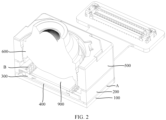
FIG. 2 is a cross-sectional view of a camera apparatus disclosed according to an embodiment of this application; -
FIG. 3 is a schematic diagram of an overall structure of a camera apparatus disclosed according to an embodiment of this application; -
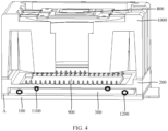
FIG. 4 is a schematic structural diagram of a camera apparatus disclosed according to an embodiment of this application; -
FIG. 5 is a schematic diagram of an exploded structure of a camera apparatus disclosed according to an embodiment of this application; -
FIG. 6 is a schematic diagram of partial structure of a camera apparatus disclosed according to an embodiment of this application; -
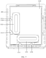
FIG. 7 is a schematic diagram of a planar structure of a first driving mechanism of a camera apparatus disclosed according to an embodiment of this application; -
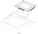
FIG. 8 is a schematic diagram of a three-dimensional structure of a first driving mechanism of a camera apparatus disclosed according to an embodiment of this application; and -
FIG. 9 is a schematic structural diagram of a photosensitive chip of a camera apparatus disclosed according to an embodiment of this application. -
- 100. supporting circuit board;
- 200. outer frame base;
- 300. inner frame base;
- 400. photosensitive chip, 410. solder ball;
- 500. lens holder;
- 600. lens;
- 700. first driving mechanism, 710. first driving sub-mechanism, 711. first electromagnetic coil, 712. first permanent magnet, 720. second driving sub-mechanism, 721. second electromagnetic coil, 722. second permanent magnet;
- 800. adjustable lens module;
- 900. filter;
- 1000. protective housing, 1000a. avoidance hole, 1000b. avoidance channel, 1000c. electrical connection pins;
- 1100. first set of rolling elements;
- 1200. second set of rolling elements;
- 1300. lifting mechanism, 1310. support portion, 1311. guide slot, 1320. second driving mechanism, 1321. third electromagnetic coil, 1322. third permanent magnet, 1330. third set of rolling elements;
- A. conductive adhesive layer, B. gold wire, and C. connective adhesive layer.
- The following clearly and completely describes the technical solutions in embodiments of this application with reference to the accompanying drawings in the embodiments of this application. Apparently, the described embodiments are only some rather than all of the embodiments of this application. All other embodiments obtained by persons of ordinary skill in the art based on the embodiments of this application without creative efforts shall fall within the protection scope of this application.
- The terms "first", "second", and the like in this specification and claims of this application are used to distinguish between similar objects rather than to describe a specific order or sequence. It should be understood that data used in this way is used interchangeably in appropriate circumstances such that the embodiments of this application can be implemented in other orders than the order illustrated or described herein. In addition, "first" and "second" are usually used to distinguish objects of a same type, and do not restrict a quantity of objects. For example, there may be one or a plurality of first objects. In addition, "and/or" in the specification and claims represents at least one of connected objects, and the character "/" generally indicates that the associated objects have an "or" relationship.
- The camera apparatus and electronic device disposed in the embodiments of this application are hereinafter described in detail by using specific embodiments and application scenarios thereof with reference to the accompanying drawings.
- As shown in
FIG. 1 to FIG. 9 , an embodiment of this application discloses a camera apparatus and an electronic device. The disclosed camera apparatus includes a supportingcircuit board 100, anouter frame base 200, aninner frame base 300, aphotosensitive chip 400, alens holder 500, alens 600, and afirst driving mechanism 700. - The supporting
circuit board 100 is capable of providing power to an electrical structure in the camera apparatus and also supporting a structure disposed on the supporting circuit board. Theinner frame base 300 and theouter frame base 200 play a role in supporting thephotosensitive chip 400, thelens holder 500, thelens 600, and thefirst driving mechanism 700, and can also facilitate an electrical connection between the supportingcircuit board 100 and thephotosensitive chip 400. - The
outer frame base 200 is disposed on the supportingcircuit board 100, and theouter frame base 200 is connected to the supportingcircuit board 100 via a conductive adhesive layer A. The conductive adhesive layer A contains conductive particles, enabling the conductive adhesive layer A to not only connect theouter frame base 200 and the supportingcircuit board 100 but also provide electrical conductivity between the two. Certainly, theouter frame base 200 can alternatively be electrically connected to the supportingcircuit board 100 in other ways. For example, theouter frame base 200 and the supportingcircuit board 100 can be electrically connected via a conductive coating layer, a soldering member, or the like. - The
lens holder 500 is disposed on theouter frame base 200, and thelens 600 is disposed on thelens holder 500, in other words, thelens 600, thelens holder 500, and theouter frame base 200 are disposed sequentially on the supportingcircuit board 100, and the supportingcircuit board 100 is electrically connected to thephotosensitive chip 400 via theouter frame base 200 and theinner frame base 300 sequentially, such that theouter frame base 200 and theinner frame base 300 can transfer electrical energy from the supportingcircuit board 100 to thephotosensitive chip 400, thus realizing the function of thephotosensitive chip 400. - The
inner frame base 300 is movably disposed on theouter frame base 200, and thephotosensitive chip 400 is disposed on theinner frame base 300, such that thephotosensitive chip 400 and the supportingcircuit board 100 are separated by theinner frame base 300 and theouter frame base 200. In this way, theinner frame base 300 can drive thephotosensitive chip 400 to move relatively without the problem of being impeded by the supportingcircuit board 100. Thephotosensitive chip 400 and thelens 600 are arranged opposite to each other, which is beneficial for the electronic device to capture high-quality pictures through thelens 600. Thefirst driving mechanism 700 is configured to drive theinner frame base 300 to move, such that thephotosensitive chip 400 is capable of performing stabilization movements along with theinner frame base 300 in a plane perpendicular to an optical axis of thelens 600. Thephotosensitive chip 400 is arranged in such a way that thephotosensitive chip 400 is separated from the supportingcircuit board 100 by theinner frame base 300 and theouter frame base 200. This enables thephotosensitive chip 400 to be electrically connected to the supportingcircuit board 100 without being affected by it. As a result, thephotosensitive chip 400, when driven to perform stabilization movements, is not affected by the supportingcircuit board 100. - The camera apparatus disclosed in the embodiments of this application is improved based on structure of the camera apparatus in the related art. With the
photosensitive chip 400 disposed on theinner frame base 300, theinner frame base 300 disposed on theouter frame base 200, theouter frame base 200 disposed on the supportingcircuit board 100, thelens holder 500 disposed on theouter frame base 200, thelens 600 disposed on thelens holder 500, theinner frame base 300 movably disposed on theouter frame base 200, and thephotosensitive chip 400 electrically connected to the supportingcircuit board 100 via theinner frame base 300 and theouter frame base 200, thelens 600, thelens holder 500, thephotosensitive chip 400, theinner frame base 300, and theouter frame base 200 are disposed sequentially on the supportingcircuit board 100, and theinner frame base 300 can drive, under driving of thefirst driving mechanism 700, thephotosensitive chip 400 to move, so as to achieve stabilization movements of the camera apparatus. In this way, thephotosensitive chip 400 is not impeded by the supportingcircuit board 100 during stabilization movements, thus solving the problem in the background that movement of the photosensitive chip under driving is impeded by the flexible circuit board. - In the camera apparatus disclosed in the embodiments of this application, the supporting
circuit board 100, theouter frame base 200, thelens holder 500, and thelens 600 can enclose a sealed space, and theinner frame base 300 and thephotosensitive chip 400 are located in the sealed space. In this case, the sealed space forms a protective structure for theinner frame base 300 and thephotosensitive chip 400. Such sealed space can prevent foreign objects such as water and dust from entering, thus providing good dust-proof and waterproof effects. In addition, it can also prevent other foreign objects from entering and falling on thephotosensitive chip 400 to affect the shooting. - In the camera apparatus disclosed in the embodiments of this application, the camera apparatus further includes an adjustable lens module (T-lens module) 800. The
adjustable lens module 800 can include a zoom area, where the zoom area is arranged opposite to thelens 600; and theadjustable lens module 800 is electrically connected to the supportingcircuit board 100, such that the zoom area and thelens 600 can cooperate to achieve the zoom function of the camera apparatus. As a result, when the distance between the camera apparatus and a shooting object changes, the camera apparatus can still shoot high-quality pictures. In the embodiments of this application, the T-lens module 800 can change the thickness of the zoom area when powered on, thereby achieving the purpose of zooming. This enables the camera apparatus to achieve zooming without a zoom motor, which not only avoids the volume and cost problems caused by the configuration of the zoom motor but also reduces the weight of the entire camera apparatus. When the camera apparatus is configured in an electronic device, it is beneficial for the development of electronic devices toward lightweight and thin design. - In a further technical solution, the camera apparatus may further include a
protective housing 1000, and theprotective housing 1000 can protect the internal structure of the camera apparatus. Theprotective housing 1000 is mounted on theouter frame base 200, theprotective housing 1000 is provided with anavoidance hole 1000a, thelens 600 and thelens holder 500 are located in theprotective housing 1000, theadjustable lens module 800 is mounted on theprotective housing 1000 and covers theavoidance hole 1000a, and thelens 600 is arranged opposite to theavoidance hole 1000a, such that when the internal structure of the camera apparatus is protected by theprotective housing 1000, thelens 600 can be arranged opposite to theadjustable lens module 800 through theavoidance hole 1000a, thereby achieving the adjustable focus shooting function of the camera apparatus. - In a more specific solution, the
first driving mechanism 700 may be a first electromagnetic driving mechanism, theprotective housing 1000 is an electromagnetic shielding housing, and theprotective housing 1000 is disposed on thefirst driving mechanism 700, such that theprotective housing 1000 can provide both protection and shielding for thefirst driving mechanism 700. This can prevent electromagnetic interference from the external environment on thefirst driving mechanism 700, thereby enabling thefirst driving mechanism 700 to stably and accurately drive theinner frame base 300. - In the camera apparatus disclosed in the embodiments of this application, the
photosensitive chip 400 can be soldered to theinner frame base 300 throughsolder balls 410 arranged in a row, and thephotosensitive chip 400 is electrically connected to theinner frame base 300 through thesolder balls 410, and/or theinner frame base 300 is electrically connected to theouter frame base 200 through gold wires B arranged in a row. In this case, thephotosensitive chip 400 is fixedly connected to theinner frame base 300 through thesolder balls 410, such that thesolder balls 410 can also play a fixing role on thephotosensitive chip 400 when electrically connecting thephotosensitive chip 400 to theinner frame base 300. Theinner frame base 300 can be electrically connected to theouter frame base 200 through the gold wires B, such that theinner frame base 300 and theouter frame base 200 can achieve relative rotation while realizing electrical connection. - In the camera apparatus disclosed in the embodiments of this application, the camera apparatus can further include a
filter 900. Thefilter 900 is disposed on theinner frame base 300, and thefilter 900 covers thephotosensitive chip 400. In this case, thefilter 900 can be connected to thephotosensitive chip 400 via a connective adhesive layer C, such that thefilter 900 can be fixed on thephotosensitive chip 400. In this way, during shooting by the camera apparatus, the external environmental light can pass through thefilter 900 first for filtering, such that the filter can filter out unwanted colors in the environmental light, thus preventing the unwanted colors from entering thephotosensitive chip 400 to affect the shooting effect of the camera apparatus. In addition, thefilter 900 is integrated on theinner frame base 300 and covers thephotosensitive chip 400, which not only protects thephotosensitive chip 400 but also facilitates more compact assembly and easy formation of modules, thereby realizing overall disassembly and assembly. - In the camera apparatus disclosed in the embodiments of this application, the
first driving mechanism 700 may include afirst driving sub-mechanism 710, the first drivingsub-mechanism 710 includes a firstelectromagnetic coil 711 and a firstpermanent magnet 712, the firstelectromagnetic coil 711 is disposed on theouter frame base 200 and electrically connected to theouter frame base 200, the firstpermanent magnet 712 is disposed on theinner frame base 300, and the first drivingsub-mechanism 710 drives theinner frame base 300 to move in the first direction relative to theouter frame base 200; and thefirst driving mechanism 700 further includes asecond driving sub-mechanism 720, thesecond driving sub-mechanism 720 includes a secondelectromagnetic coil 721 and a secondpermanent magnet 722, the secondelectromagnetic coil 721 is disposed on theouter frame base 200 and electrically connected to theouter frame base 200, and the secondpermanent magnet 722 is disposed on theinner frame base 300, where thesecond driving sub-mechanism 720 drives theinner frame base 300 to move in a second direction relative to theouter frame base 200, the first direction intersects the second direction, and a surface defined by the intersection of the first direction and the second direction is the plane. - In the above situation, in a case that the first
electromagnetic coil 711 electrically connected to theouter frame base 200 is energized, it generates a driving force on the firstpermanent magnet 712, such that theinner frame base 300 provided with the firstpermanent magnet 712 can move in the first direction under the driving of the firstelectromagnetic coil 711; similarly, in a case that the secondelectromagnetic coil 721 electrically connected to theouter frame base 200 is energized, it generates a driving force on the secondpermanent magnet 722, such that theinner frame base 300 provided with the secondpermanent magnet 722 can move in the second direction under the driving of the secondelectromagnetic coil 721. This enables thefirst driving mechanism 700 to drive theinner frame base 300 via the first drivingsub-mechanism 710 and thesecond driving sub-mechanism 720 and drive theinner frame base 300 to move in the first direction and the second direction, such that theinner frame base 300 can drive thephotosensitive chip 400 to move in the plane where the first direction and the second direction intersect for motion stabilization. This can achieve stabilization in multiple directions, which in turn can improve the stabilization performance of the camera apparatus. - In a further technical solution, a first set of rolling
elements 1100 can be disposed between theinner frame base 300 and theouter frame base 200, and theinner frame base 300 can move in the first direction via the first set of rollingelements 1100. A second set of rollingelements 1200 can be disposed between theinner frame base 300 and the supportingcircuit board 100, and theinner frame base 300 can move in the second direction via the second set of rollingelements 1200. In this case, the first set of rollingelements 1100 can assist theinner frame base 300 to move in the first direction, while the second set of rollingelements 1200 can assist theinner frame base 300 to move in the second direction, such that when theinner frame base 300 moves in the first direction and the second direction, the first set of rollingelements 1100 and the second set of rollingelements 1200 can reduce the friction between theinner frame base 300 and theouter frame base 200, making it easier for thefirst driving mechanism 700 to drive theinner frame base 300. - In the camera apparatus disclosed in the embodiments of this application, the camera apparatus can further include a
lifting mechanism 1300, thelifting mechanism 1300 is disposed in a holding space, theinner frame base 300 is connected to thelifting mechanism 1300, and thelifting mechanism 1300 drives theinner frame base 300 to drive thephotosensitive chip 400 to move along a direction of the optical axis. In this case, thephotosensitive chip 400 can be driven by theinner frame base 300 to move along the direction of the optical axis under the driving of thelifting mechanism 1300, such that thephotosensitive chip 400 can also achieve stabilization of the camera apparatus in the direction of the optical axis by movement. - In a more specific solution, the
lifting mechanism 1300 may include asupport portion 1310 and asecond driving mechanism 1320, thesecond driving mechanism 1320 is configured to drive thesupport portion 1310 to move along the optical axis, theinner frame base 300 is disposed on thesupport portion 1310, theinner frame base 300 is capable of driving thephotosensitive chip 400 to move with thesupport portion 1310, and thesecond driving mechanism 1320 is a second electromagnetic driving mechanism. In this way, thesecond driving mechanism 1320 can drive thesupport portion 1310 to move along the optical axis, and accordingly, theinner frame base 300 located on thesupport portion 1310 can be driven to move along the optical axis, ultimately enabling thephotosensitive chip 400 to move along the direction of the optical axis. The use of an electromagnetic driving mechanism as thesecond driving mechanism 1320 makes the overall structure of thelifting mechanism 1300 simple and also makes the overall volume of thelifting mechanism 1300 smaller. - In a more optimized solution, a third set of rolling
elements 1330 is disposed between thesupport portion 1310 and theouter frame base 200, thesupport portion 1310 is provided with aguide slot 1311, and the third set of rollingelements 1330 is disposed in theguide slot 1311 and is capable of rolling relative to theguide slot 1311. In this way, when thesecond driving mechanism 1320 drives thesupport portion 1310 to move along the direction of the optical axis, the third set of rollingelements 1330 can reduce the friction between theouter frame base 200 and thesupport portion 1310, which is beneficial for thesecond driving mechanism 1320 to drive thesupport portion 1310. Moreover, the setting of theguide slot 1311 allows at least a part of the third set of rollingelements 1330 to be installed in theguide slot 1311, which not only ensures the good rolling guidance effect of the third set of rollingelements 1330 but also reduces the size of the third set of rollingelements 1330 in one direction of the camera apparatus. - Based on the foregoing camera apparatus, an embodiment of this application discloses an electronic device, and the disclosed electronic device includes the camera apparatus according to any one of the above.
- The electronic device disclosed in the embodiments of this application may be a smartphone, a tablet computer, an e-book reader, a wearable device (for example, a smartwatch), a game console, or other devices. A specific type of electronic device is not limited in the embodiments of this application.
- The foregoing describes the embodiments of this application with reference to the accompanying drawings. However, this application is not limited to the foregoing specific embodiments. The foregoing specific embodiments are merely illustrative rather than restrictive. As instructed by this application, persons of ordinary skill in the art may develop many other manners without departing from principles of this application and the protection scope of the claims, and all such manners fall within the protection scope of this application.
Claims (13)
- A camera apparatus comprising a supporting circuit board (100), an outer frame base (200), an inner frame base (300), a photosensitive chip (400), a lens holder (500), a lens (600), and a first driving mechanism (700), whereinthe outer frame base (200) is disposed on the supporting circuit board (100), the lens holder (500) is disposed on the outer frame base (200), the lens (600) is disposed on the lens holder (500), and the supporting circuit board (100) is electrically connected to the photosensitive chip (400) via the outer frame base (200) and the inner frame base (300) sequentially; andthe inner frame base (300) is movably disposed on the outer frame base (200), the photosensitive chip (400) is disposed on the inner frame base (300), the photosensitive chip (400) is arranged opposite to the lens (600), the first driving mechanism (700) is configured to drive the inner frame base (300) to move, and the photosensitive chip (400) is capable of performing stabilization movements along with the inner frame base (300) in a plane perpendicular to an optical axis of the lens (600).
- The camera apparatus according to claim 1, wherein the supporting circuit board (100), the outer frame base (200), the lens holder (500), and the lens (600) enclose a sealed space, and the inner frame base (300) and the photosensitive chip (400) are located in the sealed space.
- The camera apparatus according to claim 1, wherein the camera apparatus further comprises an adjustable lens module (800), the adjustable lens module (800) comprises a zoom area, the zoom area is arranged opposite to the lens (600), and the adjustable lens module (800) is electrically connected to the supporting circuit board (100).
- The camera apparatus according to claim 3, wherein the camera apparatus further comprises a protective housing (1000), the protective housing (1000) is mounted on the outer frame base (200), the protective housing (1000) is provided with an avoidance hole (1000a), and the lens (600) and the lens holder (500) is located within the protective housing (1000), wherein the adjustable lens module (800) is mounted on the protective housing (1000) and covers the avoidance hole (1000a), and the lens (600) is arranged opposite to the avoidance hole (1000a).
- The camera apparatus according to claim 4, wherein the first driving mechanism (700) is a first electromagnetic driving mechanism, the protective housing (1000) is an electromagnetic shielding housing, and the protective housing (1000) is disposed on the first driving mechanism (700).
- The camera apparatus according to claim 1, wherein the photosensitive chip (400) is soldered to the inner frame base (300) through solder balls (410) arranged in a row, the photosensitive chip (400) is electrically connected to the inner frame base (300) through the solder balls (410), and/or the inner frame base (300) is electrically connected to the outer frame base (200) through gold wires (B) arranged in a row.
- The camera apparatus according to claim 1, wherein the camera apparatus further comprises a filter (900), the filter (900) is disposed on the inner frame base (300), and the filter (900) covers the photosensitive chip (400).
- The camera apparatus according to claim 1, wherein the first driving mechanism (700) comprises a first driving sub-mechanism (710), the first driving sub-mechanism (710) comprises a first electromagnetic coil (711) and a first permanent magnet (712), the first electromagnetic coil (711) is disposed on the outer frame base (200) and is electrically connected to the outer frame base (200), the first permanent magnet (712) is disposed on the inner frame base (300), and the first driving sub-mechanism (710) drives the inner frame base (300) to move in a first direction relative to the outer frame base (200); and
the first driving mechanism (700) further comprises a second driving sub-mechanism (720), the second driving sub-mechanism (720) comprises a second electromagnetic coil (721) and a second permanent magnet (722), the second electromagnetic coil (721) is disposed on the outer frame base (200) and electrically connected to the outer frame base (200), and the second permanent magnet (722) is disposed on the inner frame base (300); and the second driving sub-mechanism (720) drives the inner frame base (300) to move in a second direction relative to the outer frame base (200), the first direction intersects the second direction, and a surface defined by the intersection of the first direction and the second direction is the plane. - The camera apparatus according to claim 8, wherein a first set of rolling elements (1100) is disposed between the inner frame base (300) and the outer frame base (200), the inner frame base (300) moves in the first direction via the first set of rolling elements (1100), a second set of rolling elements (1200) is disposed between the inner frame base (300) and the supporting circuit board (100), and the inner frame base (300) moves in the second direction via the second set of rolling elements (1200).
- The camera apparatus according to claim 1, wherein the camera apparatus further comprises a lifting mechanism (1300), the lifting mechanism (1300) is disposed in a holding space, the inner frame base (300) is connected to the lifting mechanism (1300), and the lifting mechanism (1300) drives the inner frame base (300) to drive the photosensitive chip (400) to move along a direction of the optical axis.
- The camera apparatus according to claim 10, wherein the lifting mechanism (1300) comprises a support portion (1310) and a second driving mechanism (1320), the second driving mechanism (1320) is configured to drive the support portion (1310) to move along the optical axis, the inner frame base (300) is disposed on the support portion (1310), the inner frame base (300) is capable of driving the photosensitive chip (400) to move with the support portion (1310), and the second driving mechanism (1320) is a second electromagnetic driving mechanism.
- The camera apparatus according to claim 11, wherein a third set of rolling elements (1330) is disposed between the support portion (1310) and the outer frame base (200), the support portion (1310) is disposed with a guide slot (1311), and the third set of rolling elements (1330) is disposed in the guide slot (1311) and is capable of rolling relative to the guide slot (1311).
- An electronic device comprising the camera apparatus according to any one of claims 1 to 12.
Applications Claiming Priority (2)
| Application Number | Priority Date | Filing Date | Title |
|---|---|---|---|
| CN202110405573.2A CN113114899B (en) | 2021-04-15 | 2021-04-15 | Imaging device and electronic apparatus |
| PCT/CN2022/086139 WO2022218262A1 (en) | 2021-04-15 | 2022-04-11 | Camera apparatus and electronic device |
Publications (2)
| Publication Number | Publication Date |
|---|---|
| EP4307651A1 true EP4307651A1 (en) | 2024-01-17 |
| EP4307651A4 EP4307651A4 (en) | 2024-08-21 |
Family
ID=76717418
Family Applications (1)
| Application Number | Title | Priority Date | Filing Date |
|---|---|---|---|
| EP22787488.0A Pending EP4307651A4 (en) | 2021-04-15 | 2022-04-11 | CAMERA APPARATUS AND ELECTRONIC DEVICE |
Country Status (5)
| Country | Link |
|---|---|
| US (1) | US12501160B2 (en) |
| EP (1) | EP4307651A4 (en) |
| JP (1) | JP7731440B2 (en) |
| CN (1) | CN113114899B (en) |
| WO (1) | WO2022218262A1 (en) |
Families Citing this family (5)
| Publication number | Priority date | Publication date | Assignee | Title |
|---|---|---|---|---|
| CN116134369B (en) * | 2020-10-14 | 2025-10-31 | 宁波舜宇光电信息有限公司 | Driving structure for optical actuator, corresponding camera module and assembling method |
| CN113114899B (en) | 2021-04-15 | 2022-02-25 | 维沃移动通信有限公司 | Imaging device and electronic apparatus |
| CN116261023B (en) * | 2021-12-08 | 2026-03-24 | 宁波舜宇光电信息有限公司 | Image stabilization camera module |
| CN114637124B (en) * | 2022-04-21 | 2025-06-13 | 河南皓泽电子股份有限公司 | Base assembly and lens drive mechanism |
| CN114637123A (en) * | 2022-04-21 | 2022-06-17 | 河南皓泽电子股份有限公司 | Circuit board assembly and lens driving mechanism |
Family Cites Families (44)
| Publication number | Priority date | Publication date | Assignee | Title |
|---|---|---|---|---|
| JP3435580B2 (en) * | 1993-04-30 | 2003-08-11 | コニカ株式会社 | Zoom lens barrel and camera |
| JP3956787B2 (en) | 2002-07-10 | 2007-08-08 | コニカミノルタフォトイメージング株式会社 | Imaging device |
| JP2005062633A (en) | 2003-08-19 | 2005-03-10 | Konica Minolta Opto Inc | Lens system |
| JP2008077072A (en) | 2006-08-23 | 2008-04-03 | Konica Minolta Opto Inc | Imaging element unit and imaging apparatus |
| JP2008203433A (en) | 2007-02-19 | 2008-09-04 | Citizen Electronics Co Ltd | Camera unit |
| JP5084308B2 (en) | 2007-03-14 | 2012-11-28 | ペンタックスリコーイメージング株式会社 | Stage device and camera shake correction device using stage device |
| CN101546090B (en) * | 2008-03-25 | 2011-09-28 | 鸿富锦精密工业(深圳)有限公司 | Imaging device |
| JP5265336B2 (en) * | 2008-12-25 | 2013-08-14 | 富士フイルム株式会社 | Camera shake correction apparatus and optical apparatus |
| KR101026179B1 (en) | 2009-07-28 | 2011-04-05 | 삼성전기주식회사 | Camera module |
| JP5821356B2 (en) | 2011-07-15 | 2015-11-24 | ミツミ電機株式会社 | Lens drive device |
| KR101927237B1 (en) * | 2011-11-18 | 2018-12-10 | 엘지이노텍 주식회사 | Camera Module |
| KR101308619B1 (en) * | 2012-06-14 | 2013-09-23 | 주식회사 하이소닉 | Assembling method of compact camera actuator for aligning lens axis |
| KR101991719B1 (en) * | 2012-06-29 | 2019-06-21 | 엘지이노텍 주식회사 | Camera Module |
| TWI528809B (en) * | 2012-10-02 | 2016-04-01 | 台灣東電化股份有限公司 | Integrated substrate for anti-shake apparatus |
| TWI464479B (en) | 2013-02-08 | 2014-12-11 | Wah Hong Ind Corp | Lens activating device |
| KR102159746B1 (en) * | 2014-01-28 | 2020-09-24 | 엘지이노텍 주식회사 | Lens moving unit and camera module having the same |
| CN107615160B (en) | 2015-05-29 | 2020-06-16 | 三美电机株式会社 | Actuator, camera module, and camera-mounted device |
| CN105573014A (en) * | 2016-01-22 | 2016-05-11 | 南昌欧菲光电技术有限公司 | Camera module with focusing and anti-shaking functions |
| SG11201807830UA (en) | 2016-03-11 | 2018-10-30 | Apple Inc | Optical image stabilization with voice coil motor for moving image sensor |
| JP6772726B2 (en) | 2016-09-29 | 2020-10-21 | リコーイメージング株式会社 | Imaging device and imaging method |
| JP6779104B2 (en) * | 2016-11-10 | 2020-11-04 | 日本電産サンキョー株式会社 | Optical unit with runout correction function |
| KR102825135B1 (en) | 2017-01-26 | 2025-06-26 | 엘지이노텍 주식회사 | Liquid lens module, camera module including the same and method for manufacturing the liquid lens module |
| US10866385B2 (en) * | 2017-05-12 | 2020-12-15 | Tdk Taiwan Corp. | Optical system |
| CN109975898A (en) * | 2017-12-27 | 2019-07-05 | 华为技术有限公司 | A kind of control method of lens module and lens module |
| JP2019148698A (en) | 2018-02-27 | 2019-09-05 | ソニーセミコンダクタソリューションズ株式会社 | Camera module |
| CN108600608B (en) * | 2018-03-16 | 2019-12-31 | 维沃移动通信有限公司 | A lens holder, lens module and electronic equipment |
| US10893200B2 (en) | 2018-06-01 | 2021-01-12 | Faez Ba-Tis | Autofocus and optical image stabilizer system |
| CN116347238A (en) | 2018-06-29 | 2023-06-27 | Lg伊诺特有限公司 | Camera Units and Optical Instruments |
| JP2020036216A (en) | 2018-08-30 | 2020-03-05 | ソニーセミコンダクタソリューションズ株式会社 | Solid-state imaging apparatus and method of manufacturing the same |
| US11522472B2 (en) | 2018-09-26 | 2022-12-06 | MEMS Drive (Nanjing) Co., Ltd. | MEMS actuation system |
| CN110049235A (en) * | 2019-03-06 | 2019-07-23 | 杭州电子科技大学 | A kind of optical anti-vibration MEMS actuator |
| CN209417492U (en) | 2019-03-22 | 2019-09-20 | 高瞻创新科技有限公司 | A high-performance and reliable miniature anti-shake head |
| KR102869742B1 (en) | 2019-03-28 | 2025-10-14 | 엘지이노텍 주식회사 | camera device |
| CN110650281A (en) * | 2019-10-30 | 2020-01-03 | 维沃移动通信(杭州)有限公司 | Camera module and electronic equipment |
| US20210144483A1 (en) * | 2019-11-07 | 2021-05-13 | Innovative Interface Laboratory Corp. | Single-axis actuator, acoustic wave generator and its array |
| CN211266979U (en) * | 2020-03-19 | 2020-08-14 | 南昌欧菲光电技术有限公司 | Camera module and electronic equipment |
| CN111510598B (en) | 2020-04-17 | 2021-11-02 | 维沃移动通信有限公司 | Camera module and electronic equipment |
| CN111654612B (en) * | 2020-06-17 | 2021-09-03 | 维沃移动通信有限公司 | Camera module and electronic equipment |
| CN111726508A (en) * | 2020-07-06 | 2020-09-29 | 瑞声新能源发展(常州)有限公司科教城分公司 | Lens module |
| TWI726766B (en) | 2020-07-08 | 2021-05-01 | 大陽科技股份有限公司 | Camera module and electronic device |
| CN212935999U (en) * | 2020-08-18 | 2021-04-09 | 江西晶浩光学有限公司 | Camera module, electronic equipment and vehicle-mounted equipment |
| CN212785548U (en) * | 2020-09-21 | 2021-03-23 | 重庆市天实精工科技有限公司 | Anti-shake camera module, camera anti-shake system and mobile terminal |
| CN112637466B (en) * | 2020-12-22 | 2022-07-08 | 维沃移动通信有限公司 | Camera module and electronic equipment |
| CN113114899B (en) * | 2021-04-15 | 2022-02-25 | 维沃移动通信有限公司 | Imaging device and electronic apparatus |
-
2021
- 2021-04-15 CN CN202110405573.2A patent/CN113114899B/en active Active
-
2022
- 2022-04-11 JP JP2023562657A patent/JP7731440B2/en active Active
- 2022-04-11 EP EP22787488.0A patent/EP4307651A4/en active Pending
- 2022-04-11 WO PCT/CN2022/086139 patent/WO2022218262A1/en not_active Ceased
-
2023
- 2023-10-13 US US18/486,240 patent/US12501160B2/en active Active
Also Published As
| Publication number | Publication date |
|---|---|
| JP2024514595A (en) | 2024-04-02 |
| US12501160B2 (en) | 2025-12-16 |
| EP4307651A4 (en) | 2024-08-21 |
| US20240040257A1 (en) | 2024-02-01 |
| WO2022218262A1 (en) | 2022-10-20 |
| CN113114899A (en) | 2021-07-13 |
| CN113114899B (en) | 2022-02-25 |
| JP7731440B2 (en) | 2025-08-29 |
Similar Documents
| Publication | Publication Date | Title |
|---|---|---|
| US12501160B2 (en) | Camera apparatus and electronic device | |
| US11178323B2 (en) | Photosensitive element driving mechanism | |
| EP4212950B1 (en) | Lens driving device, camera module, and optical device | |
| EP4325834A1 (en) | Photographing apparatus and electronic device | |
| US11693213B2 (en) | Optical system | |
| CN211955944U (en) | Drive Mechanisms for Optical Components | |
| EP4213477B1 (en) | Lens driving device, camera module, and optical device | |
| CN106131386A (en) | Photographic head module and electronic equipment | |
| US11994701B2 (en) | Photosensitive module having transparent plate and image sensor | |
| EP4380173A1 (en) | Camera device and optical device | |
| US12581177B2 (en) | Camera device | |
| JP2023541178A (en) | Camera equipment and optical equipment | |
| US20260059197A1 (en) | Camera device having first and second magnets of different sizes | |
| CN113014758B (en) | Camera module and electronic equipment | |
| CN114257726B (en) | Camera module and electronic equipment | |
| US20250024149A1 (en) | Camera device | |
| JP2024519833A (en) | Camera equipment | |
| CN119071616B (en) | Camera module and electronic equipment | |
| CN120454438B (en) | Motors, camera modules, and electronic devices | |
| WO2026092365A1 (en) | Driving module, optical assembly, camera module and electronic device | |
| WO2026001586A1 (en) | Foldable circuit board structure, anti-shake gimbal, camera device and electronic apparatus | |
| CN121634652A (en) | Aperture components, camera modules and electronic devices | |
| CN120786166A (en) | Camera module and electronic equipment | |
| KR20230115475A (en) | camera device | |
| CN120786183A (en) | Camera module and electronic equipment |
Legal Events
| Date | Code | Title | Description |
|---|---|---|---|
| STAA | Information on the status of an ep patent application or granted ep patent |
Free format text: STATUS: THE INTERNATIONAL PUBLICATION HAS BEEN MADE |
|
| PUAI | Public reference made under article 153(3) epc to a published international application that has entered the european phase |
Free format text: ORIGINAL CODE: 0009012 |
|
| STAA | Information on the status of an ep patent application or granted ep patent |
Free format text: STATUS: REQUEST FOR EXAMINATION WAS MADE |
|
| 17P | Request for examination filed |
Effective date: 20231010 |
|
| AK | Designated contracting states |
Kind code of ref document: A1 Designated state(s): AL AT BE BG CH CY CZ DE DK EE ES FI FR GB GR HR HU IE IS IT LI LT LU LV MC MK MT NL NO PL PT RO RS SE SI SK SM TR |
|
| REG | Reference to a national code |
Ref country code: DE Ref legal event code: R079 Free format text: PREVIOUS MAIN CLASS: H04N0005225000 Ipc: G02B0007020000 |
|
| DAV | Request for validation of the european patent (deleted) | ||
| DAX | Request for extension of the european patent (deleted) | ||
| A4 | Supplementary search report drawn up and despatched |
Effective date: 20240722 |
|
| RIC1 | Information provided on ipc code assigned before grant |
Ipc: G02B 27/64 20060101ALI20240716BHEP Ipc: H04N 23/55 20230101ALI20240716BHEP Ipc: H04N 23/68 20230101ALI20240716BHEP Ipc: G02B 7/02 20210101AFI20240716BHEP |
|
| STAA | Information on the status of an ep patent application or granted ep patent |
Free format text: STATUS: EXAMINATION IS IN PROGRESS |
|
| 17Q | First examination report despatched |
Effective date: 20251031 |