EP4293701A2 - Ladungsteilchenstrahlvorrichtung und bilderfassungsverfahren - Google Patents
Ladungsteilchenstrahlvorrichtung und bilderfassungsverfahren Download PDFInfo
- Publication number
- EP4293701A2 EP4293701A2 EP23178104.8A EP23178104A EP4293701A2 EP 4293701 A2 EP4293701 A2 EP 4293701A2 EP 23178104 A EP23178104 A EP 23178104A EP 4293701 A2 EP4293701 A2 EP 4293701A2
- Authority
- EP
- European Patent Office
- Prior art keywords
- image
- specimen
- probe
- frame
- position shift
- Prior art date
- Legal status (The legal status is an assumption and is not a legal conclusion. Google has not performed a legal analysis and makes no representation as to the accuracy of the status listed.)
- Pending
Links
Images





Classifications
-
- H—ELECTRICITY
- H01—ELECTRIC ELEMENTS
- H01J—ELECTRIC DISCHARGE TUBES OR DISCHARGE LAMPS
- H01J37/00—Discharge tubes with provision for introducing objects or material to be exposed to the discharge, e.g. for the purpose of examination or processing thereof
- H01J37/26—Electron or ion microscopes; Electron or ion diffraction tubes
- H01J37/28—Electron or ion microscopes; Electron or ion diffraction tubes with scanning beams
-
- H—ELECTRICITY
- H01—ELECTRIC ELEMENTS
- H01J—ELECTRIC DISCHARGE TUBES OR DISCHARGE LAMPS
- H01J37/00—Discharge tubes with provision for introducing objects or material to be exposed to the discharge, e.g. for the purpose of examination or processing thereof
- H01J37/02—Details
- H01J37/22—Optical, image processing or photographic arrangements associated with the tube
- H01J37/222—Image processing arrangements associated with the tube
-
- H—ELECTRICITY
- H01—ELECTRIC ELEMENTS
- H01J—ELECTRIC DISCHARGE TUBES OR DISCHARGE LAMPS
- H01J37/00—Discharge tubes with provision for introducing objects or material to be exposed to the discharge, e.g. for the purpose of examination or processing thereof
- H01J37/02—Details
- H01J37/244—Detectors; Associated components or circuits therefor
-
- H—ELECTRICITY
- H01—ELECTRIC ELEMENTS
- H01J—ELECTRIC DISCHARGE TUBES OR DISCHARGE LAMPS
- H01J37/00—Discharge tubes with provision for introducing objects or material to be exposed to the discharge, e.g. for the purpose of examination or processing thereof
- H01J37/26—Electron or ion microscopes; Electron or ion diffraction tubes
- H01J37/261—Details
- H01J37/265—Controlling the tube; circuit arrangements adapted to a particular application not otherwise provided, e.g. bright-field-dark-field illumination
-
- H—ELECTRICITY
- H01—ELECTRIC ELEMENTS
- H01J—ELECTRIC DISCHARGE TUBES OR DISCHARGE LAMPS
- H01J2237/00—Discharge tubes exposing object to beam, e.g. for analysis treatment, etching, imaging
- H01J2237/244—Detection characterized by the detecting means
- H01J2237/2448—Secondary particle detectors
-
- H—ELECTRICITY
- H01—ELECTRIC ELEMENTS
- H01J—ELECTRIC DISCHARGE TUBES OR DISCHARGE LAMPS
- H01J2237/00—Discharge tubes exposing object to beam, e.g. for analysis treatment, etching, imaging
- H01J2237/25—Tubes for localised analysis using electron or ion beams
- H01J2237/2505—Tubes for localised analysis using electron or ion beams characterised by their application
- H01J2237/2511—Auger spectrometers
-
- H—ELECTRICITY
- H01—ELECTRIC ELEMENTS
- H01J—ELECTRIC DISCHARGE TUBES OR DISCHARGE LAMPS
- H01J2237/00—Discharge tubes exposing object to beam, e.g. for analysis treatment, etching, imaging
- H01J2237/26—Electron or ion microscopes
- H01J2237/28—Scanning microscopes
- H01J2237/2803—Scanning microscopes characterised by the imaging method
- H01J2237/2804—Scattered primary beam
-
- H—ELECTRICITY
- H01—ELECTRIC ELEMENTS
- H01J—ELECTRIC DISCHARGE TUBES OR DISCHARGE LAMPS
- H01J2237/00—Discharge tubes exposing object to beam, e.g. for analysis treatment, etching, imaging
- H01J2237/26—Electron or ion microscopes
- H01J2237/28—Scanning microscopes
- H01J2237/2803—Scanning microscopes characterised by the imaging method
- H01J2237/2806—Secondary charged particle
Definitions
- the present invention relates to a charged particle beam device and an image acquisition method.
- a scanning electron microscope (SEM), a scanning transmission electron microscope (STEM), an electron probe microanalyzer (EPMA), an Auger electron spectrometer (Auger), and so on are known as charged particle beam devices that acquire a scanned image by scanning a specimen with an electron probe.
- SEM scanning electron microscope
- STEM scanning transmission electron microscope
- EPMA electron probe microanalyzer
- Auger Auger electron spectrometer
- a specimen may drift due to heat generated in the region of the specimen that is irradiated with the electron probe, temperature unevenness on the periphery thereof, and so on. Also, the irradiation position of the electron probe may drift due to temperature variation in the optical system and so on. When relative positions of the electron probe and the specimen change over time in this manner, it is impossible to acquire a scanned image with a high degree of positional accuracy. Therefore, in a charged particle beam device capable of observation and analysis at a high magnification of 100,000 times or more, a function for correcting the irradiation position of the electron probe is required.
- JP-A-2000-348172 discloses a method for detecting position shift between two images by determining a correlation function between the images from a product of Fourier transforms, wherein an inverse Fourier transform is performed by multiplying the real part of a Fourier component of a correlation by an integer smaller than 1 so that a correlation peak due to fixed noise becomes smaller than a peak representing a net position shift. Based on the position shift between the images, the irradiation position of an electron probe can be corrected.
- JP-A-2015-210999 discloses a charged particle beam device that corrects the irradiation position of an electron probe by calculating a drift amount based on a cross-correlation function between a base image and a comparison image, and deflecting an electron beam based on the drift amount.
- an image of a specimen can be acquired by repeatedly scanning an observation region of the specimen with an electron probe so as to acquire a plurality of frame images, and integrating the plurality of frame images.
- an image of a specimen is acquired by integrating a plurality of frame images in this manner and the drift amount is large, position shift occurs between the frame images even if the position of the electron probe is corrected for each frame.
- position shift occurs between the frame images, blurring occurs on the image of the specimen after the frame images are integrated.
- a charged particle beam device that acquires an image by scanning a specimen with a probe formed from a charged particle beam and detecting a signal emitted from the specimen, the charged particle beam device including:
- an image acquisition method employed in a charged particle beam device that acquires an image by scanning a specimen with a probe formed from a charged particle beam and detecting a signal emitted from the specimen, the image acquisition method including:
- a charged particle beam device that acquires an image by scanning a specimen with a probe formed from a charged particle beam and detecting a signal emitted from the specimen, the charged particle beam device including:
- the position shift of each frame image is corrected as well as correcting the irradiation position of the probe, making it possible to correct position shift between the frame images, which cannot be corrected by correcting the irradiation position of the probe.
- image blurring caused by position shifting between the frame images can be reduced, and as a result, a clear image of the specimen can be acquired.
- an image acquisition method employed in a charged particle beam device that acquires an image by scanning a specimen with a probe formed from a charged particle beam and detecting a signal emitted from the specimen, the image acquisition method including:
- the position shift of each frame image is corrected as well as correcting the irradiation position of the probe, making it possible to correct position shift between the frame images, which cannot be corrected by correcting the irradiation position of the probe.
- image blurring caused by position shifting between the frame images can be reduced, and as a result, a clear image of the specimen can be acquired.
- FIG. 1 is a diagram illustrating a configuration of an Auger electron spectrometer 100 according to the first embodiment.
- the Auger electron spectrometer 100 performs measurements using Auger electron spectroscopy.
- Auger electron spectroscopy is a method for performing element analysis by measuring the energy of Auger electrons that are excited by an electron beam or the like and emitted from a specimen.
- the Auger electron spectrometer 100 includes an optical system 20, a specimen stage 30, an electron spectrometer 50, a secondary electron detector 70, a control unit 80, a storage unit 82, and an image processing unit 90.
- the optical system 20 is an electron optical system that forms a probe using an electron beam and scans a specimen S with the probe.
- the optical system 20 includes an electron source 21, a condenser lens 22, a deflector 24, a scanning deflector 25, and an objective lens 26.
- the electron source 21 emits the electron beam.
- the electron source 21 is an electron gun that emits an electron beam by accelerating electrons emitted from a cathode using an acceleration voltage applied between the cathode and an anode.
- the condenser lens 22 and the objective lens 26 form the electron probe by condensing the electron beam emitted from the electron source 21.
- the scanning deflector 25 two-dimensionally deflects the electron beam condensed by the condenser lens 22 and the objective lens 26. By deflecting the electron beam two-dimensionally using the scanning deflector 25, the specimen S can be scanned by the electron probe.
- the deflector 24 two-dimensionally deflects the condensed electron beam.
- the deflector 24 is used, for example, in image shifting for electromagnetically moving the field of view of the scanned image.
- the specimen stage 30 holds the specimen S.
- the specimen stage 30 includes, for example, a horizontal direction moving mechanism for moving the specimen S in a horizontal direction, a height direction moving mechanism for moving the specimen S in a height direction, and a tilting mechanism for tilting the specimen S.
- the specimen stage 30 can be used to position the specimen S.
- the electron spectrometer 50 analyzes the Auger electrons.
- the electron spectrometer 50 is a hemispherical electrostatic analyzer, for example.
- the electron spectrometer 50 includes an inner hemispherical electrode and an outer hemispherical electrode.
- the electron spectrometer 50 applies a voltage between the inner hemispherical electrode and the outer hemispherical electrode and thereby detects Auger electrons in an energy range corresponding to the applied voltage.
- an Auger spectrum can be acquired.
- an Auger image can be acquired.
- the Auger image is an image showing the strength distribution of the Auger electrons on the specimen S.
- the secondary electron detector 70 detects secondary electrons emitted from the specimen S when the specimen S is irradiated with the electron beam. By scanning the specimen S with the electron probe and measuring the number of secondary electrons (the strength of the secondary electrons) at each point on the specimen S, a secondary electron image can be acquired.
- the Auger electron spectrometer 100 may also include a backscattered-electron detector that detects backscattered electrons emitted from the specimen S when the specimen S is irradiated with the electron beam. By scanning the specimen S with the electron probe and measuring the number of backscattered electrons at each point on the specimen S, a backscattered electron image can be acquired.
- the control unit 80 controls the optical system 20. Further, the control unit 80 repeatedly performs correction processing for correcting shifting of the irradiation position of the electron probe on the specimen S and image acquisition processing for acquiring a frame image by causing the optical system 20 to scan an observation region of the specimen S using the electron probe.
- the processing performed by the control unit 80 will be described in detail below in "1.2.1. Processing of control unit”.
- the control unit 80 includes, for example, a processor such as a CPU (Central Processing Unit) or a DSP (Digital Signal Processor), and a storage device (a RAM (Random Access Memory), a ROM (Read Only Memory), and so on).
- a processor such as a CPU (Central Processing Unit) or a DSP (Digital Signal Processor)
- a storage device a RAM (Random Access Memory), a ROM (Read Only Memory), and so on.
- Various types of calculation processing and various types of control processing are performed in the control unit 80 by executing a program stored in the storage device using the processor.
- the storage unit 82 stores the images acquired by the control unit 80.
- the storage unit 82 includes, for example, a RAM, a hard disk, or the like.
- the image processing unit 90 generates an image of the specimen S.
- the image processing unit 90 generates an image of the specimen S based on a plurality of frame images.
- the processing performed by the image processing unit 90 will be described in detail below in "1.2.2. Processing of image processing unit".
- the image processing unit 90 includes, for example, a processor such as a CPU or a DSP, and a storage device such as a RAM or a ROM. Various types of calculation processing and various types of control processing are performed in the image processing unit 90 by executing a program stored in the storage device using the processor.
- FIG. 2 is a diagram for describing scanning performed by the electron probe of the Auger electron spectrometer 100.
- the electron probe is formed by condensing the electrons emitted from the electron source 21 using the condenser lens 22 and the objective lens 26, whereupon the specimen S is scanned with the electron probe by deflecting the electron beam using the scanning deflector 25.
- the electron probe By scanning the specimen S with the electron probe, analyzing the Auger electrons emitted from each point on the specimen S using the electron spectrometer 50, and detecting Auger electrons of specific energy values, an Auger image can be acquired.
- a secondary electron image can be acquired.
- Auger electron spectrometer 100 As illustrated in FIG. 2 , raster scanning is performed on an observation region S2 of the specimen S. For example, as illustrated in FIG. 2 , a scan is performed using the electron probe by repeatedly drawing scanning lines L along the X axis and moving the position in which the scanning lines L are drawn along the Y axis. By scanning the observation region S2 with the electron probe once, a single frame image F can be acquired. In the Auger electron spectrometer 100, a plurality of frame images F are acquired by repeatedly scanning the observation region S2 with the electron probe, and a single image (an Auger image) of the specimen S is generated based on the plurality of frame images F. By generating the image of the specimen S based on the plurality of frame images F, damage to the specimen S caused by the electron beam can be reduced, and at the same time, an image with reduced noise can be acquired.
- FIG. 3 is a flowchart illustrating an example of the processing performed by the control unit 80 of the Auger electron spectrometer 100.
- the Auger electron spectrometer 100 when acquiring an Auger image will be described.
- a user Before the control unit 80 executes processing for acquiring the Auger image, a user sets conditions (the acceleration voltage, the probe current, and so on) of the optical system 20 and conditions of the electron spectrometer 50 for acquiring the Auger image.
- the user sets these conditions by operating a setting unit (a user interface or the like) of the control unit 80.
- the settings of these conditions in the setting unit are reflected in the processing performed by the control unit 80.
- the user determines the observation region S2 on the specimen S. For example, the user observes the specimen S by acquiring a secondary electron image of the specimen S in the Auger electron spectrometer 100, and determines the observation region S2.
- the user After determining the conditions of the optical system 20, the conditions of the electron spectrometer 50, and the observation region S2, the user instructs the Auger electron spectrometer 100 to start acquiring an Auger image.
- the control unit 80 determines whether or not the user has issued an instruction to start acquiring an Auger image (S 100). The control unit 80 determines that the user has issued a start instruction when a depression operation has been performed on a start button or a start instruction has been input from an input device.
- control unit 80 acquires a base image (S 102).
- the base image is an image that serves as a position reference of the Auger image.
- the base image is a secondary electron image.
- the control unit 80 causes the optical system 20 to scan the observation region S2 with the electron probe and acquires data of the base image (a secondary electron image) from the secondary electron detector 70.
- the base image may be acquired after the observation region S2 has been determined and before the start instruction has been issued.
- control unit 80 performs correction processing for correcting shifting of the irradiation position of the electron probe on the specimen S (S 104).
- the correction processing S 104 will be described below.
- control unit 80 performs image acquisition processing for acquiring the frame image F (S 106).
- the control unit 80 acquires data of a frame image F of the Auger image by causing the optical system 20 to scan the observation region S2 with the electron probe.
- the frame image F of the Auger image is an Auger image acquired by scanning the observation region S2 once.
- the control unit 80 stores the frame image F in the storage unit 82.
- control unit 80 determines whether or not a set number of frame images F has been acquired (S 108).
- the control unit 80 counts the frame images F stored in the storage unit 82 and determines whether or not a preset number of frame images F has been acquired.
- the control unit 80 Having determined that the set number of frame images F has not been acquired (No in S 108), the control unit 80 performs the correction processing S 104, the image acquisition processing S 106, and the determination processing S 108. The control unit 80 repeats the correction processing S104 and the image acquisition processing S106 until it is determined that the set number of frame images F has been acquired. The control unit 80 performs the correction processing S104 and the image acquisition processing S 106 for each frame.
- the control unit 80 After determining that the set number of frame images F has been acquired (Yes in S 108), the control unit 80 terminates the processing. Thus, the set number of frame images F can be acquired.
- the correction processing S104 may be performed after the image acquisition processing S106.
- FIG. 4 is a flowchart illustrating an example of the correction processing S104.
- control unit 80 acquires a reference image by causing the optical system 20 to scan the observation region S2 with the electron probe (S140).
- the reference image is a secondary electron image of the observation region S2.
- the control unit 80 acquires data of the reference image (a secondary electron image) from the secondary electron detector 70 by causing the optical system 20 to scan the observation region S2 with the electron probe.
- the control unit 80 records the secondary electron image acquired as the reference image in the storage unit 82.
- the control unit 80 determines a position shift amount and a position shift direction between the base image and the reference image (a secondary electron image) (S142).
- the control unit 80 determines the position shift amount and the position shift direction between the base image and the reference image by pattern matching, for example.
- the position shift amount and the position shift direction may be determined by performing Fourier transforms respectively on the base image and the reference image and calculating a correlation function between the result of the Fourier transform performed on the base image and the result of the Fourier transform performed on the reference image.
- the control unit 80 may determine the position shift amount and the position shift direction between the base image and the reference image using the method described in JP-A-2000-348172 .
- control unit 80 determines whether or not the position shift amount between the base image and the reference image equals or exceeds a predetermined amount (S143).
- the predetermined amount can be set by the user at any desired value.
- control unit 80 corrects shifting of the irradiation position of the electron probe on the specimen S by operating the optical system 20 based on the position shift amount and the position shift direction between the base image and the reference image (S 144).
- the control unit 80 operates the optical system 20 based on the position shift amount and the position shift direction between the base image and the reference image so as to cancel shifting of the irradiation position of the electron probe on the specimen S. For example, shifting of the irradiation position is corrected by deflecting the electron beam using the deflector 24 so as to move the irradiation position of the electron probe by the position shift amount in an opposite direction to the position shift direction.
- the scanning deflector 25 then performs a scan using the electron probe in a state where the position shift of the electron probe has been corrected by the deflector 24. Thus, a scan can be performed using the electron probe in a state where the irradiation position of the electron probe has been corrected.
- control unit 80 After operating the optical system 20 so as to cancel shifting of the irradiation position of the electron probe, or after determining that the position shift amount between the base image and the reference image does not equal or exceed the predetermined amount (No in S143), the control unit 80 terminates the correction processing.
- the image processing unit 90 generates an image of the specimen S based on the plurality of frame images F acquired by repeatedly performing the image acquisition processing S106.
- FIG. 5 is a flowchart illustrating an example of the processing performed by the image processing unit 90.
- FIG. 6 is a diagram for describing the processing performed by the image processing unit 90.
- the image processing unit 90 acquires the base image, a plurality of reference images, and a plurality of frame images F by reading the base image, the plurality of reference images, and the plurality of frame images F recorded in the storage unit 82 (S200).
- the image processing unit 90 acquires position shift information indicating the position shift between the base image and each reference image (S202).
- the image processing unit 90 positions the reference image relative to the base image by performing a geometrical transformation, or more specifically an affine transformation (parallel movement, rotation, scaling, and so on), on the reference image based on the mutual information amount between the base image and the reference image.
- the image processing unit 90 acquires position shift information indicating the position shift between the base image and each reference image.
- the position shift information is information relating to the position shift between the base image and each reference image, and includes information such as the position shift amount, the position shift direction, rotation, scaling, and so on between the base image and each reference image.
- the image processing unit 90 corrects the position shift of each frame image F based on the position shift information indicating the position shift between the base image and each reference image (S204).
- the correction processing S104 described above is performed for each frame, the reference image and the frame image F are acquired for each frame. Accordingly, the position shift of each frame image F is corrected based on the position shift information indicating the position shift between the base image and the reference image acquired in the same frame as the corresponding frame image F.
- the image processing unit 90 moves the position (the coordinates) of each frame image F by the position shift amount in the opposite direction to the position shift direction between the base image and the corresponding reference image. For example, the image processing unit 90 moves the position (the coordinates) of the frame image F of a first frame by the position shift amount between the base image and the reference image of the first frame in the opposite direction to the position shift direction between the base image and the reference image of the first frame.
- the coordinates of each pixel constituting the frame image F of the first frame are modified by the position shift amount in the opposite direction to the position shift direction.
- the image processing unit 90 corrects the rotation of the frame image F of the first frame based on the rotation between the base image and the reference image of the first frame.
- the image processing unit 90 enlarges or reduces the frame image F of the first frame based on the scaling factor between the base image and the reference image of the first frame.
- the image processing unit 90 then performs similar processing to that of the frame image F of the first frame on the frame images F of the second frame onward, and in so doing corrects the position shift of each frame image F.
- the image processing unit 90 generates an image IS (an Auger image) of the specimen S based on the plurality of frame images F in which the position shift has been corrected (S206).
- the image processing unit 90 superimposes the plurality of frame images F in which the position shift has been corrected, and averages or integrates the pixel values of the pixels having the same coordinates.
- the image IS an Auger image
- the pixel values are values expressing the brightness of the pixels, and correspond to the number of Auger electrons (the strength of the Auger electrons).
- the Auger image (the image IS) is a grayscale image, and the number of Auger electrons (the strength of the Auger electrons) is expressed by the brightness of each pixel.
- the control unit 80 repeatedly performs the correction processing S104 for correcting shifting of the irradiation position of the electron probe on the specimen S and the image acquisition processing S106 for acquiring the frame images F by causing the optical system 20 to scan the observation region S2 of the specimen S with the electron probe. Further, the image processing unit 90 generates the image IS of the specimen S based on the plurality of frame images F. Furthermore, in the correction processing S 104, the control unit 80 acquires a reference image by causing the optical system 20 to scan the observation region S2 with the electron probe, and corrects shifting of the irradiation position of the electron probe based on the position shift amount between the base image and the reference image. Moreover, the image processing unit 90 corrects position shift between the frame images F based on the position shift information indicating the position shift between the base image and each reference image, and generates an image of the specimen S based on the plurality of corrected frame images F.
- the position shift of each frame image F is corrected as well as correcting the irradiation position of the electron probe, making it possible to correct position shift between the frame images F, which cannot be corrected by correcting the irradiation position of the electron probe. Accordingly, with the Auger electron spectrometer 100, image blurring caused by position shifting between the frame images F can be reduced, whereby a clear image IS of the specimen S can be acquired. As a result, the spatial resolution of the Auger image can be improved.
- the reference image is a secondary electron image
- the frame image F is an Auger image.
- a secondary electron image an image with little noise can be acquired in a shorter time than an Auger image. Therefore, by using a secondary electron image as the reference image, the correction processing S104 can be performed accurately in a short amount of time.
- control unit 80 acquires a secondary electron image as the reference image in the correction processing S 104, and acquires an Auger image as the frame image F in the image acquisition processing S106.
- the control unit 80 may acquire the reference image simultaneously with the Auger image.
- the Auger electron spectrometer 100 as illustrated in FIG. 1 , both the electron spectrometer 50 for detecting Auger electrons and the secondary electron detector 70 are provided, and therefore Auger electrons and secondary electrons can be detected simultaneously.
- Auger electrons using the electron spectrometer 50 and detecting secondary electrons using the secondary electron detector 70 during a single scan of the observation region S2 an Auger image (a frame image) and a reference image can be acquired simultaneously.
- FIG. 7 is a diagram illustrating a configuration of an Auger electron spectrometer 200 according to the second embodiment.
- members of the Auger electron spectrometer 200 according to the second embodiment that have similar functions to the constituent members of the Auger electron spectrometer 100 according to the first embodiment have been allocated identical reference numerals, and detailed description thereof has been omitted.
- the Auger electron spectrometer 100 described above, as illustrated in FIG. 1 includes the electron spectrometer 50 and the secondary electron detector 70.
- the Auger electron spectrometer 200 on the other hand, as illustrated in FIG. 7 , a secondary electron detector is not provided.
- the base image and the reference image are secondary electron images
- the frame image F is an Auger image
- the base image, the reference image, and the frame image F are Auger images.
- FIG. 8 is a flowchart illustrating an example of the processing performed by the control unit 80 of the Auger electron spectrometer 200. Below, points that differ from the example of the Auger electron spectrometer 100 illustrated in FIG. 3 will be described, while description of similar points will be omitted.
- the control unit 80 determines whether or not the user has issued an instruction to start acquiring an Auger image (S300).
- control unit 80 acquires the base image (S302).
- the control unit 80 acquires an Auger image as the base image. More specifically, the control unit 80 causes the optical system 20 to scan the observation region S2 with the electron probe, and acquires data of the Auger image from the electron spectrometer 50. Note that the Auger image acquired as the base image is also used as the frame image F of the first frame.
- control unit 80 performs image acquisition processing for acquiring the frame image F (S304).
- the image acquisition processing S304 is performed in a similar manner to the image acquisition processing 5106 described above.
- the frame image F of the second frame is acquired.
- control unit 80 performs correction processing for correcting shifting of the irradiation position of the electron probe on the specimen S (S306).
- the correction processing S306 is performed in a similar manner to the correction processing S104 illustrated in FIG. 4 except that the Auger image of the first frame, acquired in the processing of S302, is used as the base image, and the Auger image of the second frame is used as the reference image.
- control unit 80 determines whether or not the set number of frame images F has been acquired (S308).
- the determination processing S308 is performed in a similar manner to the determination processing S108 described above.
- the control unit 80 Having determined that the set number of frame images F has not been acquired (No in S308), the control unit 80 performs the image acquisition processing S304, the correction processing S306, and the determination processing S308.
- the correction processing S306 the Auger image of the first frame, acquired in the processing of S302, is used as the base image, and an Auger image of a third frame, acquired in the image acquisition processing S304, is used as the reference image.
- the control unit 80 repeats the image acquisition processing S304, the correction processing S306, and the determination processing S308 until it is determined that the set number of frame images F has been acquired. Thus, the control unit 80 performs the image acquisition processing S304 and the correction processing S306 for each frame.
- the control unit 80 After determining that the set number of frame images F has been acquired (Yes in S308), the control unit 80 terminates the processing. Thus, the set number of frame images F can be acquired.
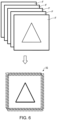
- FIG. 9 illustrates a secondary electron image of lead-free solder, a gross Auger image of lead-free solder, and a net Auger image of lead-free solder.
- the gross Auger image is an image showing the strength distribution in a peak position of an Auger spectrum.
- the net Auger image is obtained by subtracting the strength in a background position from the strength in the peak position of the Auger spectrum.
- the gross Auger image has a large S/N ratio (signal to noise ratio) and therefore resembles a secondary electron image. Accordingly, the gross Auger image is suitable as the base image and the reference image.
- the processing of the image processing unit 90 of the Auger electron spectrometer 200 is similar to the processing of the image processing unit 90 of the Auger electron spectrometer 100 illustrated in FIG. 5 , and therefore description thereof has been omitted.
- the reference image and the frame image F are Auger images.
- the reference image and the frame image F are the same, and therefore it is not necessary to acquire a secondary electron image as the reference image, for example.
- the plurality of frame images F can be acquired in a short amount of time.
- An Auger electron spectrometer according to the third embodiment is configured similarly to the Auger electron spectrometer 100 illustrated in FIG. 1 , and therefore description thereof has been omitted.
- control unit 80 performed the correction processing S104 for each frame, whereas in the Auger electron spectrometer according to the third embodiment, the control unit 80 performs the correction processing for each 1/N (where N is an integer of 2 or more) of a frame.
- FIG. 10 is a flowchart illustrating an example of the processing performed by the control unit 80 of the Auger electron spectrometer according to the third embodiment.
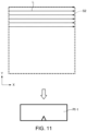
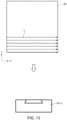
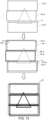
- FIGS. 11-13 are diagrams illustrating operations of the Auger electron spectrometer according to the third embodiment. Below, points that differ from the example of the Auger electron spectrometer 100 illustrated in FIG. 3 will be described, while description of similar points will be omitted.
- the control unit 80 acquires the base image (S402) after determining that the user has issued a start instruction (Yes in S400).
- the processing of S402 for acquiring the base image is performed in a similar manner to the processing of S102 for acquiring the base image, as illustrated in FIG. 3 .
- the base image may be acquired after the observation region S2 has been determined and before the start instruction has been issued.
- control unit 80 performs correction processing for correcting shifting of the irradiation position of the electron probe on the specimen S (S404).
- the correction processing S404 is performed in a similar manner to the correction processing S 104.
- the control unit 80 acquires a partial image PI-1 by causing the optical system 20 to scan the observation region S2 by an amount corresponding to 1/N (where N is an integer of 2 or more) of a frame (S406).
- N is an integer of 2 or more
- the observation region S2 is divided into 3.
- N 3.
- the number of parts into which the observation region S2 is divided may be set as desired.
- the control unit 80 stores the acquired partial image PI-1 in the storage unit 82.
- control unit 80 determines whether or not partial images have been acquired for 1 frame (S408).
- the observation region S2 is divided into 3, and therefore the control unit 80 determines that partial images have been acquired for 1 frame when three partial images PI-1, PI-2, and PI-3 have been acquired.
- the control unit 80 performs the correction processing S404 so as to acquire the partial image PI-2, as illustrated in FIG. 12 (S406).
- the control unit 80 performs the correction processing S404 so as to acquire the partial image PI-3, as illustrated in FIG. 13 (S406).
- the partial images PI-1, PI-2, and PI-3 corresponding to 1 frame can be acquired.
- a single frame image F can be acquired.
- control unit 80 determines whether or not the set number of frame images F has been acquired (S410).
- control unit 80 Having determined that the set number of frame images F has not been acquired (No in S410), the control unit 80 performs the correction processing S404, the image acquisition processing S406, the determination processing S408, and the determination processing S410. The control unit 80 repeats the correction processing S404, the image acquisition processing S406, the determination processing S408, and the determination processing S410 until it is determined that the set number of frame images F has been acquired.
- the control unit 80 After determining that the set number of frame images F has been acquired (Yes in S410), the control unit 80 terminates the processing.
- a plurality of partial images constituting the set number of frame images F can be acquired. For example, when the number of frame images F is set at 10, 10 ⁇ N partial images can be acquired.
- the image processing unit 90 generates an image of the specimen S based on the plurality of acquired partial images.
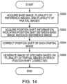
- FIG. 14 is a flowchart illustrating an example of the processing performed by the image processing unit 90.
- FIG. 15 is a diagram for describing the processing performed by the image processing unit 90. Below, points that differ from the example of the Auger electron spectrometer 100 illustrated in FIG. 5 will be described, while description of similar points will be omitted.
- the image processing unit 90 acquires the base image, a plurality of reference images, and a plurality of partial images by reading the base image, the plurality of reference images, and the plurality of partial images recorded in the storage unit 82 (S500).
- the image processing unit 90 acquires position shift information indicating the position shift between the base image and each reference image (S502).
- the image processing unit 90 acquires the position shift information indicating the position shift between the base image and each reference image using a similar method to that of the processing of S202 illustrated in FIG. 5 for acquiring the position shift information indicating the position shift between the base image and the reference image.
- the image processing unit 90 corrects the position shift of each partial image based on the position shift information indicating the position shift between the base image and each reference image (S504).
- the correction processing S 104 is performed for each 1/N of a frame, and therefore a reference image and a partial image are acquired for each 1/N of a frame. Accordingly, the position shift of each partial image is corrected based on position shift information indicating the position shift between the base image and the reference images acquired in the same frame as the partial images.
- the image processing unit 90 generates an image (an Auger image) of the specimen S based on the plurality of partial images in which the position shift has been corrected (S506).
- the image processing unit 90 superimposes the plurality of partial images, and when two or more pixels exist at the same coordinates, determines the average of the pixel values and sets the result as a pixel value of the image IS of the specimen S. Further, when one pixel exists at the same coordinates, the image processing unit 90 sets the pixel value of that one pixel as a pixel value of the image IS of the specimen S.
- the partial image PI-1 and the partial image PI-4 are superimposed in a position P1 having coordinates (X1, Y1). Accordingly, the pixel value of the pixel at the coordinates (X1, Y1) of the partial image PI-1 and the pixel value of the pixel at the coordinates (X1, Y1) of the partial image PI-4 are averaged, and the result is set as the pixel value of the pixel at the coordinates (X1, Y1) of the image IS. Likewise in a case where three or more partial images are superimposed in a predetermined position, the average of the pixel values of the partial images is set as the pixel value of the corresponding pixel of the image IS.
- the partial image PI-4 exists, and therefore the pixel value of the pixel at the coordinates (X2, Y2) of the partial image PI-4 is set as the pixel value of the pixel at the coordinates (X2, Y2) of the image IS.
- pixel values of pixels of the image IS that correspond to a gap 2 between adjacent partial images are determined based on the pixel values of another frame image F.
- the gap 2 exists between the adjacent partial images PI-2 and PI-3.
- the partial image PI-6 among the three partial images PI-4, PI-5, and PI-6 constituting another frame image F, overlaps the gap 2. Therefore, the pixel values of the pixels of the partial image PI-6 overlapping the gap 2 are used as the pixel values of the pixels of the image IS that correspond to the region of the gap 2.
- blank parts generated in one frame image F when the position shift of the partial images is corrected are compensated for using the pixel values of another frame image F.
- the image processing unit 90 generates the image IS of the specimen S based on the plurality of partial images in which position shift has been corrected.
- the control unit 80 performs the correction processing S404 for each 1/N of a frame, and in the image acquisition processing S406, the control unit 80 acquires a partial image by causing the optical system 20 to scan the observation region S2 by an amount corresponding to 1/N of a frame, and acquires each frame image F by repeating the correction processing S404 and the image acquisition processing S406 N times.
- the correction processing S404 is performed for each 1/N of a frame, and therefore, in comparison with a case where the correction processing is performed for each frame, for example, shifting of the irradiation position of the electron probe can be corrected at shorter time intervals.
- the image processing unit 90 corrects the position shift between the partial images based on the position shift information indicating the position shift between the base image and the reference images, and generates the image IS of the specimen S based on the plurality of corrected partial images.
- shifting of the irradiation position of the electron probe can be corrected at shorter time intervals.
- the image processing unit 90 superimposes the plurality of corrected partial images, and when two or more pixels exist at the same coordinates, determines the average of the pixel values and sets the result as a pixel value of the image IS of the specimen S. Further, when one pixel exists at the same coordinates, the image processing unit 90 sets the pixel value of that one pixel as a pixel value of the image IS of the specimen S.
- the pixel values do not increase in accordance with the number of superimposed partial images, and therefore pixel value differences due to differences in the number of superimposed partial images do not appear on the image IS.
- the image processing unit 90 determines the pixel values of the pixels of the image IS of the specimen S that correspond to the gaps 2 between adjacent partial images of the N partial images constituting one of the plurality of frame images F based on the pixel values of another of the plurality of frame images F.
- the blank part when a blank part not having a pixel value occurs in one frame image F constituted by N partial images, the blank part can be compensated for using the pixel values of another frame image F.
- the image IS of the specimen S is generated by integrating or averaging the plurality of acquired frame images after acquiring all of the frame images, but instead, the processing for acquiring the frame images and the image processing for integrating or averaging the frame images may be performed in parallel, and an image of the specimen S may be displayed on a display unit such as a display in real time.
- the charged particle beam device according to the invention may be any device that forms a probe from a charged particle beam such as an electron beam or an ion beam and acquires a scanned image by scanning a specimen with the probe.
- signals generated by the specimen when the specimen is scanned with the probe may be electrons such as secondary electrons, backscattered electrons, or Auger electrons, X-rays such as characteristic X-rays, inelastically scattered electrons, or light such as cathode luminescence.
- the charged particle beam device may also be, for example, a scanning electron microscope (SEM), a scanning transmission electron microscope (STEM), an electron probe microanalyzer (EPMA), or a secondary ion mass spectrometer (SIMS).
- SEM scanning electron microscope
- STEM scanning transmission electron microscope
- EPMA electron probe microanalyzer
- SIMS secondary ion mass spectrometer
- the charged particle beam device may acquire various images of the specimen S other than an Auger image.
- a secondary electron image, a backscattered electron image, an element map acquired by EDS (energy dispersive X-ray spectroscopy), an element map acquired by WDS (wavelength-dispersive X-ray spectroscopy), or an element map acquired by EELS (electron energy loss spectroscopy) may be acquired as the image of the specimen S.
- the base image and the reference image are not limited to secondary electron images, and backscattered electron images, Auger images, element maps acquired by EDS, element maps acquired by EELS, and so on may be used instead.
- the invention includes configurations that are substantially the same as the configurations described in the embodiments.
- Substantially same configurations mean configurations having the same functions or methods, for example.
- the invention also includes configurations obtained by replacing non-essential elements of the configurations described in the embodiments with other elements.
- the invention further includes configurations obtained by adding known art to the configurations described in the embodiments.
Landscapes
- Chemical & Material Sciences (AREA)
- Analytical Chemistry (AREA)
- Engineering & Computer Science (AREA)
- Computer Vision & Pattern Recognition (AREA)
- Analysing Materials By The Use Of Radiation (AREA)
Applications Claiming Priority (1)
| Application Number | Priority Date | Filing Date | Title |
|---|---|---|---|
| JP2022095078A JP7576592B2 (ja) | 2022-06-13 | 2022-06-13 | 荷電粒子線装置および画像取得方法 |
Publications (2)
| Publication Number | Publication Date |
|---|---|
| EP4293701A2 true EP4293701A2 (de) | 2023-12-20 |
| EP4293701A3 EP4293701A3 (de) | 2024-04-10 |
Family
ID=86732853
Family Applications (1)
| Application Number | Title | Priority Date | Filing Date |
|---|---|---|---|
| EP23178104.8A Pending EP4293701A3 (de) | 2022-06-13 | 2023-06-07 | Ladungsteilchenstrahlvorrichtung und bilderfassungsverfahren |
Country Status (3)
| Country | Link |
|---|---|
| US (1) | US12431326B2 (de) |
| EP (1) | EP4293701A3 (de) |
| JP (1) | JP7576592B2 (de) |
Families Citing this family (1)
| Publication number | Priority date | Publication date | Assignee | Title |
|---|---|---|---|---|
| JP7465299B2 (ja) * | 2022-03-23 | 2024-04-10 | 日本電子株式会社 | 荷電粒子線装置 |
Citations (2)
| Publication number | Priority date | Publication date | Assignee | Title |
|---|---|---|---|---|
| JP2000348172A (ja) | 1999-06-03 | 2000-12-15 | Jeol Ltd | 画像間の位置ずれ検出方法 |
| JP2015210999A (ja) | 2014-04-30 | 2015-11-24 | 日本電子株式会社 | ドリフト量計算装置、ドリフト量計算方法、および荷電粒子線装置 |
Family Cites Families (10)
| Publication number | Priority date | Publication date | Assignee | Title |
|---|---|---|---|---|
| JPH05290787A (ja) * | 1992-04-08 | 1993-11-05 | Jeol Ltd | 走査電子顕微鏡 |
| JP2000106121A (ja) * | 1998-07-29 | 2000-04-11 | Jeol Ltd | 電子顕微鏡あるいはその類似装置 |
| JP4281184B2 (ja) | 1999-12-06 | 2009-06-17 | 株式会社島津製作所 | 分析装置 |
| JP3741012B2 (ja) | 2001-09-17 | 2006-02-01 | 株式会社日立製作所 | 電子線分析方法 |
| US7361894B2 (en) * | 2002-10-22 | 2008-04-22 | Hitachi High-Technologies Corporation | Method of forming a sample image and charged particle beam apparatus |
| JP4065847B2 (ja) * | 2001-11-21 | 2008-03-26 | 株式会社日立ハイテクノロジーズ | 試料像形成方法及び荷電粒子線装置 |
| WO2003044821A1 (en) | 2001-11-21 | 2003-05-30 | Hitachi High-Technologies Corporation | Sample imaging method and charged particle beam system |
| JP5500974B2 (ja) | 2009-12-25 | 2014-05-21 | 株式会社日立ハイテクノロジーズ | パターン測定装置 |
| JP6468160B2 (ja) | 2015-10-16 | 2019-02-13 | 株式会社島津製作所 | 走査型荷電粒子顕微鏡 |
| JP6662654B2 (ja) | 2016-02-12 | 2020-03-11 | 東方晶源微電子科技(北京)有限公司 | 画像取得方法及び電子ビーム検査・測長装置 |
-
2022
- 2022-06-13 JP JP2022095078A patent/JP7576592B2/ja active Active
-
2023
- 2023-06-07 EP EP23178104.8A patent/EP4293701A3/de active Pending
- 2023-06-12 US US18/208,598 patent/US12431326B2/en active Active
Patent Citations (2)
| Publication number | Priority date | Publication date | Assignee | Title |
|---|---|---|---|---|
| JP2000348172A (ja) | 1999-06-03 | 2000-12-15 | Jeol Ltd | 画像間の位置ずれ検出方法 |
| JP2015210999A (ja) | 2014-04-30 | 2015-11-24 | 日本電子株式会社 | ドリフト量計算装置、ドリフト量計算方法、および荷電粒子線装置 |
Also Published As
| Publication number | Publication date |
|---|---|
| US12431326B2 (en) | 2025-09-30 |
| JP2023181757A (ja) | 2023-12-25 |
| JP7576592B2 (ja) | 2024-10-31 |
| EP4293701A3 (de) | 2024-04-10 |
| US20230402252A1 (en) | 2023-12-14 |
Similar Documents
| Publication | Publication Date | Title |
|---|---|---|
| US5608218A (en) | Scanning electron microscope | |
| US10976536B2 (en) | Image-forming device, and dimension measurement device | |
| EP1102031B1 (de) | Verfahren und Apparat zur Messung von Musterdimensionen | |
| JP4426871B2 (ja) | Fib/sem複合装置の画像ノイズ除去 | |
| US7012252B2 (en) | Method and an apparatus of an inspection system using an electron beam | |
| JP2005310602A (ja) | 荷電粒子線調整方法、及び荷電粒子線装置 | |
| EP3985711A1 (de) | Ladungsteilchenstrahlvorrichtung | |
| US12431326B2 (en) | Charged particle beam device and image acquisition method | |
| US20060219907A1 (en) | Charged particle beam apparatus, method of displaying sample image, and method of measuring image shift sensitivity | |
| US12597582B2 (en) | Charged particle beam apparatus | |
| JP5478427B2 (ja) | 画像形成装置 | |
| JP4431624B2 (ja) | 荷電粒子線調整方法、及び荷電粒子線装置 | |
| EP4365580A1 (de) | Analyseverfahren und analysegerät mit einem wellenlängendispersiven röntgenspektrometer | |
| US12631578B2 (en) | Analyzing method and analyzer | |
| JP2015138609A (ja) | レシピ設定装置及びそれを有する荷電粒子線装置 | |
| JP2002075263A (ja) | 電子線装置 | |
| JP2010016007A (ja) | 荷電粒子線調整方法及び荷電粒子線装置 | |
| JPH0696711A (ja) | 走査電子顕微鏡像の表示方法 | |
| JP2019039765A (ja) | 荷電粒子線装置 |
Legal Events
| Date | Code | Title | Description |
|---|---|---|---|
| PUAI | Public reference made under article 153(3) epc to a published international application that has entered the european phase |
Free format text: ORIGINAL CODE: 0009012 |
|
| STAA | Information on the status of an ep patent application or granted ep patent |
Free format text: STATUS: THE APPLICATION HAS BEEN PUBLISHED |
|
| AK | Designated contracting states |
Kind code of ref document: A2 Designated state(s): AL AT BE BG CH CY CZ DE DK EE ES FI FR GB GR HR HU IE IS IT LI LT LU LV MC ME MK MT NL NO PL PT RO RS SE SI SK SM TR |
|
| PUAL | Search report despatched |
Free format text: ORIGINAL CODE: 0009013 |
|
| AK | Designated contracting states |
Kind code of ref document: A3 Designated state(s): AL AT BE BG CH CY CZ DE DK EE ES FI FR GB GR HR HU IE IS IT LI LT LU LV MC ME MK MT NL NO PL PT RO RS SE SI SK SM TR |
|
| RIC1 | Information provided on ipc code assigned before grant |
Ipc: H01J 49/08 20060101ALI20240306BHEP Ipc: H01J 37/26 20060101ALI20240306BHEP Ipc: H01J 37/244 20060101ALI20240306BHEP Ipc: H01J 37/22 20060101ALI20240306BHEP Ipc: G06T 7/32 20170101ALI20240306BHEP Ipc: H01J 37/28 20060101AFI20240306BHEP |
|
| STAA | Information on the status of an ep patent application or granted ep patent |
Free format text: STATUS: REQUEST FOR EXAMINATION WAS MADE |
|
| 17P | Request for examination filed |
Effective date: 20241004 |
|
| RBV | Designated contracting states (corrected) |
Designated state(s): AL AT BE BG CH CY CZ DE DK EE ES FI FR GB GR HR HU IE IS IT LI LT LU LV MC ME MK MT NL NO PL PT RO RS SE SI SK SM TR |