EP4293650A1 - Flexible display module and electronic device - Google Patents
Flexible display module and electronic device Download PDFInfo
- Publication number
- EP4293650A1 EP4293650A1 EP22752210.9A EP22752210A EP4293650A1 EP 4293650 A1 EP4293650 A1 EP 4293650A1 EP 22752210 A EP22752210 A EP 22752210A EP 4293650 A1 EP4293650 A1 EP 4293650A1
- Authority
- EP
- European Patent Office
- Prior art keywords
- gap
- display module
- flexible display
- side wall
- flexible substrate
- Prior art date
- Legal status (The legal status is an assumption and is not a legal conclusion. Google has not performed a legal analysis and makes no representation as to the accuracy of the status listed.)
- Pending
Links
Images




Classifications
-
- G—PHYSICS
- G06—COMPUTING OR CALCULATING; COUNTING
- G06F—ELECTRIC DIGITAL DATA PROCESSING
- G06F1/00—Details not covered by groups G06F3/00 - G06F13/00 and G06F21/00
- G06F1/16—Constructional details or arrangements
- G06F1/1613—Constructional details or arrangements for portable computers
- G06F1/1633—Constructional details or arrangements of portable computers not specific to the type of enclosures covered by groups G06F1/1615 - G06F1/1626
- G06F1/1637—Details related to the display arrangement, including those related to the mounting of the display in the housing
- G06F1/1641—Details related to the display arrangement, including those related to the mounting of the display in the housing the display being formed by a plurality of foldable display components
-
- G—PHYSICS
- G09—EDUCATION; CRYPTOGRAPHY; DISPLAY; ADVERTISING; SEALS
- G09F—DISPLAYING; ADVERTISING; SIGNS; LABELS OR NAME-PLATES; SEALS
- G09F9/00—Indicating arrangements for variable information in which the information is built-up on a support by selection or combination of individual elements
- G09F9/30—Indicating arrangements for variable information in which the information is built-up on a support by selection or combination of individual elements in which the desired character or characters are formed by combining individual elements
- G09F9/301—Indicating arrangements for variable information in which the information is built-up on a support by selection or combination of individual elements in which the desired character or characters are formed by combining individual elements flexible foldable or roll-able electronic displays, e.g. thin LCD, OLED
-
- G—PHYSICS
- G06—COMPUTING OR CALCULATING; COUNTING
- G06F—ELECTRIC DIGITAL DATA PROCESSING
- G06F1/00—Details not covered by groups G06F3/00 - G06F13/00 and G06F21/00
- G06F1/16—Constructional details or arrangements
- G06F1/1613—Constructional details or arrangements for portable computers
- G06F1/1633—Constructional details or arrangements of portable computers not specific to the type of enclosures covered by groups G06F1/1615 - G06F1/1626
- G06F1/1637—Details related to the display arrangement, including those related to the mounting of the display in the housing
- G06F1/1652—Details related to the display arrangement, including those related to the mounting of the display in the housing the display being flexible, e.g. mimicking a sheet of paper, or rollable
-
- G—PHYSICS
- G09—EDUCATION; CRYPTOGRAPHY; DISPLAY; ADVERTISING; SEALS
- G09F—DISPLAYING; ADVERTISING; SIGNS; LABELS OR NAME-PLATES; SEALS
- G09F9/00—Indicating arrangements for variable information in which the information is built-up on a support by selection or combination of individual elements
- G09F9/30—Indicating arrangements for variable information in which the information is built-up on a support by selection or combination of individual elements in which the desired character or characters are formed by combining individual elements
- G09F9/33—Indicating arrangements for variable information in which the information is built-up on a support by selection or combination of individual elements in which the desired character or characters are formed by combining individual elements being semiconductor devices, e.g. diodes
-
- H—ELECTRICITY
- H10—SEMICONDUCTOR DEVICES; ELECTRIC SOLID-STATE DEVICES NOT OTHERWISE PROVIDED FOR
- H10K—ORGANIC ELECTRIC SOLID-STATE DEVICES
- H10K59/00—Integrated devices, or assemblies of multiple devices, comprising at least one organic light-emitting element covered by group H10K50/00
- H10K59/10—OLED displays
- H10K59/12—Active-matrix OLED [AMOLED] displays
- H10K59/122—Pixel-defining structures or layers, e.g. banks
-
- H—ELECTRICITY
- H10—SEMICONDUCTOR DEVICES; ELECTRIC SOLID-STATE DEVICES NOT OTHERWISE PROVIDED FOR
- H10K—ORGANIC ELECTRIC SOLID-STATE DEVICES
- H10K77/00—Constructional details of devices covered by this subclass and not covered by groups H10K10/80, H10K30/80, H10K50/80 or H10K59/80
- H10K77/10—Substrates, e.g. flexible substrates
- H10K77/111—Flexible substrates
-
- H—ELECTRICITY
- H10—SEMICONDUCTOR DEVICES; ELECTRIC SOLID-STATE DEVICES NOT OTHERWISE PROVIDED FOR
- H10W—GENERIC PACKAGES, INTERCONNECTIONS, CONNECTORS OR OTHER CONSTRUCTIONAL DETAILS OF DEVICES COVERED BY CLASS H10
- H10W70/00—Package substrates; Interposers; Redistribution layers [RDL]
- H10W70/60—Insulating or insulated package substrates; Interposers; Redistribution layers
- H10W70/67—Insulating or insulated package substrates; Interposers; Redistribution layers characterised by their insulating layers or insulating parts
- H10W70/688—Flexible insulating substrates
-
- H—ELECTRICITY
- H10—SEMICONDUCTOR DEVICES; ELECTRIC SOLID-STATE DEVICES NOT OTHERWISE PROVIDED FOR
- H10W—GENERIC PACKAGES, INTERCONNECTIONS, CONNECTORS OR OTHER CONSTRUCTIONAL DETAILS OF DEVICES COVERED BY CLASS H10
- H10W90/00—Package configurations
-
- H—ELECTRICITY
- H10—SEMICONDUCTOR DEVICES; ELECTRIC SOLID-STATE DEVICES NOT OTHERWISE PROVIDED FOR
- H10H—INORGANIC LIGHT-EMITTING SEMICONDUCTOR DEVICES HAVING POTENTIAL BARRIERS
- H10H20/00—Individual inorganic light-emitting semiconductor devices having potential barriers, e.g. light-emitting diodes [LED]
- H10H20/80—Constructional details
- H10H20/85—Packages
- H10H20/855—Optical field-shaping means, e.g. lenses
-
- H—ELECTRICITY
- H10—SEMICONDUCTOR DEVICES; ELECTRIC SOLID-STATE DEVICES NOT OTHERWISE PROVIDED FOR
- H10K—ORGANIC ELECTRIC SOLID-STATE DEVICES
- H10K2102/00—Constructional details relating to the organic devices covered by this subclass
- H10K2102/301—Details of OLEDs
- H10K2102/311—Flexible OLED
-
- H—ELECTRICITY
- H10—SEMICONDUCTOR DEVICES; ELECTRIC SOLID-STATE DEVICES NOT OTHERWISE PROVIDED FOR
- H10W—GENERIC PACKAGES, INTERCONNECTIONS, CONNECTORS OR OTHER CONSTRUCTIONAL DETAILS OF DEVICES COVERED BY CLASS H10
- H10W70/00—Package substrates; Interposers; Redistribution layers [RDL]
- H10W70/60—Insulating or insulated package substrates; Interposers; Redistribution layers
- H10W70/611—Insulating or insulated package substrates; Interposers; Redistribution layers for connecting multiple chips together
-
- Y—GENERAL TAGGING OF NEW TECHNOLOGICAL DEVELOPMENTS; GENERAL TAGGING OF CROSS-SECTIONAL TECHNOLOGIES SPANNING OVER SEVERAL SECTIONS OF THE IPC; TECHNICAL SUBJECTS COVERED BY FORMER USPC CROSS-REFERENCE ART COLLECTIONS [XRACs] AND DIGESTS
- Y02—TECHNOLOGIES OR APPLICATIONS FOR MITIGATION OR ADAPTATION AGAINST CLIMATE CHANGE
- Y02E—REDUCTION OF GREENHOUSE GAS [GHG] EMISSIONS, RELATED TO ENERGY GENERATION, TRANSMISSION OR DISTRIBUTION
- Y02E10/00—Energy generation through renewable energy sources
- Y02E10/50—Photovoltaic [PV] energy
- Y02E10/549—Organic PV cells
Definitions
- This application belongs to the technical field of communication devices, and particularly to a flexible display module and an electronic device.
- Electronic devices such as a mobile phone and a tablet computer play an increasingly important role in people's work, life, entertainment, and other aspects.
- a display module is a main component for realizing a display function of the electronic device.
- a foldable flexible display module emerges.
- the existing flexible display module can be folded or stretched.
- the flexible display module has a relatively small volume, and is convenient to carry.
- an effective display area of the flexible display module increases, thereby improving the display performance of the electronic device.
- the flexible display module is formed by stacking and encapsulating a plurality of material layers, and the plurality of material layers are subjected to significant stress, which can easily cause the material layers to crack or drape. As a result, the display performance of the flexible display module is poor.
- the embodiments of this application aim to provide a flexible display module and an electronic device, which can solve the problem of poor display performance of the flexible display module.
- a flexible display module including:
- the embodiments of this application provide an electronic device, including the above flexible display module.
- the flexible substrate has the folding region; the folding region is provided with the first gap; the first gap extends from the first side surface to the second side surface in the thickness direction of the flexible substrate.
- the pixel units adjacent to the first gap are spaced apart from the first gap.
- the two adjacent pixel units adjacent to the first gap are separated from the first gap, which reduces the pulling stress and the extrusion stress between the pixel units, thereby reducing a surface stress of the flexible display module in the folded state.
- the flexible display module is not easy to crack or drape, making the flexible display module have relatively good display performance.
- 100 flexible display module; 110: pixel unit; 120: flexible substrate; 121: folding region; 122: first gap; 1221: first side wall; 1222: second side wall; 1223: third side wall; 1224: fourth side wall; 1225: fifth side wall; 130: routing layer; 131: first routing section; 132: second routing section; 140: separation column; 141: second gap; 151: pixel drive unit; 152: pixel drive layer; 1521: third gap; 161: first encapsulation layer; 1611: fourth gap; and 162: second encapsulation layer.
- the flexible display module 100 disclosed is applied to an electronic device, and can be used for displaying pictures, texts, videos, and other information, thereby realizing a display function of the electronic device.
- the flexible display module 100 may be folded, so that a display area of the flexible display module 100 can be adjusted, which can improve the use performance of the electronic device.
- the flexible display module 100 disclosed includes a flexible substrate 120 and a plurality of pixel units 110.
- the flexible substrate 120 provide a mounting basis for other components of the flexible display module 100.
- the flexible substrate 120 has a folding region 121.
- the flexible substrate 120 can be folded from the folding region 121.
- the folding region 121 is provided with first gaps 122.
- the first gap 122 extends from a first side surface to a second side surface in a thickness direction of the flexible substrate 120.
- a first preset distance is reserved between one end of the first gap 122 and the second side surface of the flexible substrate 120.
- the first gap 122 penetrates through the flexible substrate 120 along a lengthwise direction or a width direction of the flexible substrate 120.
- the first gaps 122 penetrate through the flexible substrate 120 along the width direction of the flexible substrate 120.
- a penetration direction of the first gaps 122 is related to a folding direction of the flexible display module 100. Therefore, the first gaps 122 can be flexibly set according to a specific folding direction of the flexible substrate 120, which is not limited herein.
- the flexible substrate 120 may be made of a highly-flexible material such as plastic.
- the first gap 122 does not penetrate through the flexible substrate 120 in the thickness direction, ensuring that the flexible substrate 120 on both sides of the first gap 122 is hard to break.
- the lengthwise direction or the width direction of the flexible substrate 120 penetrates through the flexible substrate 120, so that the flexible substrate 120 is convenient to fold. This setting manner will not affect the connection strength of the flexible substrate 120, so that the flexible substrate 120 is hard to break.
- the plurality of pixel units 110 are distributed on the first side surface of the flexible substrate 120 at intervals, and the pixel units 110 adjacent to the first gap 122 are spaced apart from the first gap 122.
- the pixel unit 110 is the smallest display unit of the flexible display module 100.
- the pixel unit 110 is used for emitting light to realize a display function of the flexible display module 100.
- the first gaps 122 are opened.
- the first gaps 122 are closed.
- the first gaps 122 of the flexible substrate 120 are opened, which reduces a pulling stress on the first side surface and an extrusion stress on the second side surface, thereby eliminating some stress that is concentrated in the folding region 121 and causing a relatively low stress on the folding region 121.
- the two adjacent pixel units 110 adjacent to the first gap 122 are separated from the first gap 122, which reduces the pulling stress and the extrusion stress between the pixel units 110, thereby reducing a surface stress of the flexible display module 100 in the folded state.
- the flexible substrate 120 is not easy to crack or drape, making the flexible display module 100 have relatively good display performance.
- the first gaps 122 are closed, which will not affect the normal display function of the flexible display module 100.
- the adjacent pixel units 110 need to be separated from each other. That is, the adjacent pixel units 110 are arranged independently without any connection relationship. Therefore, a pixel layer needs to be cut into a plurality of relatively independent pixel units 110.
- the flexible display module 100 may be a Micro LED (Micro Light Emitting Diode) flexible display module.
- the pixel units 110 of the Micro LED flexible display module are prepared independently, so that the pixel layer of the flexible display module can be segmented to obtain the plurality of segmented pixel units 110.
- the flexible display module 100 may be folded by bending. That is, the flexible display module 100 is bent into two opposite portions, as shown in FIG. 2 . Or, the flexible display module 100 may be stretched. That is, the folding region 121 itself has elasticity. When the folding region 121 is subjected to a pulling force, the folding region 121 is stretched, causing the flexible display module 100 to be unfolded. When the pulling force on the flexible display module 100 is removed, the folding region 121 retracts to restore the folded state, as shown in FIG. 5 to FIG. 8 .
- the flexible display module 100 in FIG. 5 and FIG. 6 is in the folded state, so the first gaps 122 are closed.
- the flexible display module 100 in FIG. 7 and FIG. 8 is in the unfolded state, so the first gaps 122 are opened.
- the flexible substrate 120 may also include a routing layer 130 in the lengthwise direction or the width direction of the flexible substrate, and the routing layer 130 spans an opening of the first gap 122. At this time, a routing direction of the routing layer 130 is perpendicular to the penetration direction of the first gap. When the flexible substrate 120 is folded, the routing layer 130 is easily tightened, which easily causes the routing layer 130 to be broken.
- the routing layer 130 may include a first routing section 131 and a second routing section 132.
- the first routing section 131 and the second routing section 132 may be at least partially located in the first gap 122.
- One end of the first routing section 131 located in the first gap 122 may be movably connected to one end of the second routing section 132 located in the first gap 122.
- the first routing section 131 and the second routing section 132 are movably connected, so when the first gap 122 is opened, the first routing section 131 and the second routing section 132 move in directions away from each other. When the first gap 122 is closed, the first routing section 131 and the second routing section 132 move in directions close to each other. Therefore, positions of the first routing section 131 and the second routing section 132 can be adjusted according to a state of the flexible display module 100, so that the routing layer 130 is hard to break, thereby improving the safety and reliability of the flexible display module 100.
- first routing section 131 and the second routing section 132 may be of coated structures.
- the first routing section 131 and the second routing section 132 may be both coated on side walls of the first gap 122.
- the coated structures are thinner, so that a width of the first gap 122 can be set smaller, thereby not easily affecting the display effect of the flexible display module 100.
- a processing technology of the coated structures is simple and has low cost. Specifically, mask plates are formed on the first side surface and the side walls of the first gap 122 through vacuum sputtering, and circuit patterns are obtained by exposing, etching, and demolding the mask plates.
- one end of the first routing section 131 and one end of the second routing section 132 can be hinged so that the first routing section 131 and the second routing section 132 may rotate relatively in the opening process of the first gap 122.
- a portion of the first routing section 131 located inside the first gap 122 may be a first portion, and a portion of the first routing section 131 located outside the first gap 122 is a second portion.
- a portion of the second routing section 132 located inside the first gap 122 is a third portion, and a portion of the second routing section 132 located outside the first gap 122 is a fourth portion.
- the first portion, the second portion, the third portion, and the fourth portion mentioned above are for ease of description.
- the first gap is filled with the first portion and the third portion.
- the flexible display module disclosed in this application may also include a plurality of separation columns 140.
- the separation columns 140 may be arranged on the first side surface. At least one separation column 140 may be arranged between two adjacent pixel units 110, and the first gaps 122 may be located between the separation columns 140 and the pixel units 110.
- the separation columns 140 block light emitted by the pixel units 110, which can prevent cross color between two adjacent pixel units and prevent the mutual influence of the pixel units 110, thereby improving the display performance of the flexible display module 100.
- the separation columns 140 may be provided with a second gap 141.
- the second gap 141 may penetrate through the separation columns 140, and the second gap 141 may be opposite to the first gap 122. This solution can further reduce the stress on the separation columns 140 in the folding region 121, thereby prolonging the service lives of the separation columns 140.
- the flexible display module 100 may also include a plurality of pixel drive units 151.
- Each of the pixel drive units 151 is electrically connected to one pixel unit 110.
- the pixel drive units 151 adjacent to the first gap 122 may be spaced apart from the first gap 122.
- each of the pixel drive units 151 controls one pixel unit 110, thereby realizing independent driving for each of the pixel units 110 and improving the display performance of the display module.
- two adjacent pixel drive units 151 adjacent to the first gap 122 are separated from the first gap 122, thereby reducing the pulling stress and the extrusion stress between the pixel drive units 151, so that the pixel drive units 151 are hard to damage. Meanwhile, the surface stress of the flexible display module 100 in the folded state is also further reduced.
- the pixel drive unit 151 may be a TFT (Thin Film Transistor), and of course, it may also be of other structures, which is not limited herein.
- TFT Thin Film Transistor
- the pixel drive unit 151 mentioned above is arranged independently.
- This application further discloses a drive structure of another kind of pixel unit 110.
- the flexible display module 100 disclosed in this application may also include a pixel drive layer 152.
- the pixel drive layer 152 may be arranged between the pixel units 110 and the flexible substrate 120.
- the plurality of pixel units 110 are electrically connected to the pixel drive layer 152.
- the pixel drive layer 152 may be provided with a third gap 1521.
- the third gap 1521 may penetrate through the pixel drive layer 152.
- the third gap 1521 may be opposite to the first gap 122.
- the pixel drive layer 152 is equivalent to an integrated structure formed by integrating the pixel drive units 151 in the above embodiment onto one flexible substrate.
- the pixel drive layer 152 is superimposed with the flexible substrate 120, which is equivalent to increasing a thickness of the flexible substrate 120, thereby enhancing the strength of the flexible display module 100 and preventing breakage of the flexible display module 100, so as to improve the safety and reliability of the flexible display module 100.
- the pixel drive layer 152 is provided with the third gap 1521 opposite to the first gap 122. Therefore, when the pixel drive layer 152 is folded, the third gaps 1521 can eliminate some stress concentrated on the pixel drive layer 152, so that the flexible display module 100 is hard to crack or drape, which further improves the display performance of the flexible display module.
- the pixel drive layer 152 and the pixel units 110 may be encapsulated in the same encapsulation layer, but this encapsulation structure leads to poor water oxidation resistance performance of the flexible display module 100, thereby shortening the service life of the flexible display module 100.
- the flexible display module 100 disclosed in this application may include a first encapsulation layer 161 and a plurality of second encapsulation layers 162.
- the first encapsulation layer 161 may be located between the pixel units 110 and the pixel drive layer 152. At this time, the first encapsulation layer 161 may be used for encapsulating the pixel drive layer 152.
- the first encapsulation layer 161 is provided with a fourth gap 1611.
- the fourth gap 1611 may penetrate through the first encapsulation layer 161, and the fourth gap 1611 may be opposite to the third gap 1521.
- Each of the second encapsulation layers 162 encapsulates one pixel unit 110, and each of the first gaps 122 may be located between two adjacent second encapsulation layers 162.
- the first encapsulation layer 161 is used for encapsulating the pixel drive layer 152
- the second encapsulation layers 162 are used for encapsulating the pixel units 110. Therefore, the pixel drive layer 152 and the pixel units 110 are separately encapsulated, thereby improving the water oxidation resistance performance of the flexible display module 100 and prolonging the service life of the flexible display module 100.
- the first encapsulation layer 161 is provided with the fourth gap 1611 opposite to the third gap 1521, and the third gap 1521 can eliminate some stress concentrated on the first encapsulation layer 161.
- each of the first gaps 122 may be located between two adjacent second encapsulation layers 162, so that the two second encapsulation layers 162 are separated from the first gap 122, thereby reducing the pulling stress and the extrusion stress between the second encapsulation layers 162 and further reducing the stress on the flexible display module 100 in the folded state.
- first encapsulation layer 161 and the second encapsulation layers 162 may be made of synthetic resin.
- first encapsulation layer 161 and the second encapsulation layers 162 may also be made of other materials, which is not limited herein.
- the pixel units 110 need to be electrically connected to the pixel drive layer 152, so an avoidance hole can be formed on the first encapsulation layer 161 to facilitate the electrical connection between the pixel units 110 and the pixel drive layer 152.
- each of the pixel units 110 cooperates with one pixel drive unit 151, one pixel unit 110 and one pixel drive unit 151 are encapsulated together.
- the first encapsulation layer 161 encapsulates the pixel drive layer 152 and the separation columns 140 together.
- the first gap 122 may have various structures. Referring to FIG. 2 , the first gap 122 may include a first side wall 1221 and a second side wall 1222 opposite to each other. One side of the first side wall 1221 away from the pixel unit 110 and one side of the second side wall 1222 away from the pixel unit are intersected. At this time, the first gap 122 is of a V-shaped groove structure when the first gap 122 is opened. The first gap 122 is of a linear structure when the first gap 122 is closed.
- the first side wall 1221 and the second side wall 1222 may abut against together. Therefore, when the flexible display module 100 is in the unfolded state, the first gap 122 does not easily affect the display performance of the flexible module, thereby making the flexible display module 100 have better display performance in the unfolded state.
- the first gap 122 may include a third side wall 1223, a fourth side wall 1224, and a fifth side wall 1225.
- the third side wall 1223 and the fifth side wall 1225 are opposite to each other, and the fourth side wall 1224 may be arranged between the third side wall 1223 and the fifth side wall 1225, and is connected to the third side wall 1223 and the fifth side wall 1225.
- the first gap 122 may be of a rectangular groove structure or trapezoidal groove structure.
- the first gap 122 has a relatively large size, making it easier for the flexible display module 100 to deform during folding, so that the flexible display module 100 is easier to be folded.
- the relatively large size of the first gap 122 can further reduce the stress on the flexible display module 100, thereby further preventing the flexible display module 100 from draping and cracking.
- the embodiments of this application further disclose an electronic device, the electronic device disclosed includes the flexible display module 100 of any one of the above embodiments.
- the electronic device disclosed in the embodiments of this application may be a smartphone, a tablet computer, an e-book reader, a wearable device (such as a smartwatch), an electronic game console, and the like.
- the embodiments of this application do not limit the specific type of the electronic device.
Landscapes
- Engineering & Computer Science (AREA)
- Theoretical Computer Science (AREA)
- Physics & Mathematics (AREA)
- General Physics & Mathematics (AREA)
- Computer Hardware Design (AREA)
- Human Computer Interaction (AREA)
- General Engineering & Computer Science (AREA)
- Microelectronics & Electronic Packaging (AREA)
- Devices For Indicating Variable Information By Combining Individual Elements (AREA)
- Electroluminescent Light Sources (AREA)
Abstract
Description
- This application claims priorities to
Chinese Patent Application No. 202110175261.7, filed with the China National Intellectual Property Administration on February 9, 2021 - This application belongs to the technical field of communication devices, and particularly to a flexible display module and an electronic device.
- With the rapid development of electronic devices, the electronic devices are used in more and more fields. Electronic devices such as a mobile phone and a tablet computer play an increasingly important role in people's work, life, entertainment, and other aspects.
- A display module is a main component for realizing a display function of the electronic device. With the continuous improvement of science and technology and increasingly high demands of people, a foldable flexible display module emerges. The existing flexible display module can be folded or stretched. When the flexible display module is folded, the flexible display module has a relatively small volume, and is convenient to carry. When the flexible display module is unfolded, an effective display area of the flexible display module increases, thereby improving the display performance of the electronic device.
- In the process of realizing this invention, the inventor has found the following problems existing in the relevant technology. The flexible display module is formed by stacking and encapsulating a plurality of material layers, and the plurality of material layers are subjected to significant stress, which can easily cause the material layers to crack or drape. As a result, the display performance of the flexible display module is poor.
- The embodiments of this application aim to provide a flexible display module and an electronic device, which can solve the problem of poor display performance of the flexible display module.
- To solve the above technical problem, this application is realized below:
- The embodiments of this application provide a flexible display module, including:
- a flexible substrate, where the flexible substrate has a folding region; the folding region is provided with a first gap; the first gap extends from a first side surface to a second side surface in a thickness direction of the flexible substrate; a first preset distance is reserved between one end of the first gap and the second side surface of the flexible substrate; the first gap penetrates through the flexible substrate along a lengthwise direction or a width direction of the flexible substrate; and
- a plurality of pixel units, where the plurality of pixel units are distributed on the first side surface of the flexible substrate at intervals, and the pixel units adjacent to the first gap are spaced apart from the first gap.
- The embodiments of this application provide an electronic device, including the above flexible display module.
- In the embodiments of this application, the flexible substrate has the folding region; the folding region is provided with the first gap; the first gap extends from the first side surface to the second side surface in the thickness direction of the flexible substrate. The pixel units adjacent to the first gap are spaced apart from the first gap. When the flexible display module is folded, the first gap is opened. When the flexible display module is unfolded, the first gap is closed. In this solution, when the flexible display module is folded, the first gap of the flexible substrate is opened, which reduces a pulling stress on the first side surface and an extrusion stress on the second side surface, thereby eliminating some stress that is concentrated in the folding region and causing a relatively low stress on the folding region. Meanwhile, the two adjacent pixel units adjacent to the first gap are separated from the first gap, which reduces the pulling stress and the extrusion stress between the pixel units, thereby reducing a surface stress of the flexible display module in the folded state. Thus, the flexible display module is not easy to crack or drape, making the flexible display module have relatively good display performance.
-
-
FIG. 1 is a schematic structural diagram of a first kind of flexible display module in an unfolded state according to an embodiment of this application; -
FIG. 2 is a schematic structural diagram of a first kind of flexible display module in a folded state according to an embodiment of this application; -
FIG. 3 is a schematic structural diagram of a second kind of flexible display module in an unfolded state according to an embodiment of this application; -
FIG. 4 is a schematic structural diagram of a second kind of flexible display module in a folded state according to an embodiment of this application; -
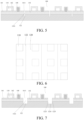
FIG. 5 and FIG. 6 are schematic structural diagrams of a third kind of flexible display module in an unfolded state according to an embodiment of this application; -
FIG. 7 andFIG. 8 are schematic structural diagrams of a third kind of flexible display module in a folded state according to an embodiment of this application; -
FIG. 9 is a partially enlarged diagram of a flexible display module in a folded state according to an embodiment of this application; and -
FIG. 10 is a partially enlarged diagram of a flexible display module in an unfolded state according to an embodiment of this application. - 100: flexible display module; 110: pixel unit; 120: flexible substrate; 121: folding region; 122: first gap; 1221: first side wall; 1222: second side wall; 1223: third side wall; 1224: fourth side wall; 1225: fifth side wall; 130: routing layer; 131: first routing section; 132: second routing section; 140: separation column; 141: second gap; 151: pixel drive unit; 152: pixel drive layer; 1521: third gap; 161: first encapsulation layer; 1611: fourth gap; and 162: second encapsulation layer.
- The technical solutions in the embodiments of this application are clearly and completely described below with reference to the accompanying drawings in the embodiments of this application. Apparently, the described embodiments are merely some rather than all of the embodiments of this application. All other embodiments obtained by an ordinary person skilled in the art based on the embodiments of this application without making creative efforts shall fall within the protection scope of this application.
- This specification and claims of this application, and terms "first" and "second" are used to distinguish similar objects, but are unnecessarily used to describe a specific sequence or order. It is to be understood that such used data is interchangeable where appropriate, so that the embodiments of this application described here can be implemented in an order other than those illustrated or described here. In addition, "and/or" used in this specification and the claims represents at least one of the connected objects. Symbol "f" usually represents an "or" relationship between front and back associated objects.
- The flexible display module provided by the embodiments of this application will be described in detail below in conjunction with the accompanying drawings through specific embodiments and application scenarios thereof.
- Referring to
FIG. 1 to FIG. 10 , the embodiments of this application discloses a flexible display module. Theflexible display module 100 disclosed is applied to an electronic device, and can be used for displaying pictures, texts, videos, and other information, thereby realizing a display function of the electronic device. Theflexible display module 100 may be folded, so that a display area of theflexible display module 100 can be adjusted, which can improve the use performance of the electronic device. Theflexible display module 100 disclosed includes aflexible substrate 120 and a plurality ofpixel units 110. - The
flexible substrate 120 provide a mounting basis for other components of theflexible display module 100. Theflexible substrate 120 has afolding region 121. Theflexible substrate 120 can be folded from thefolding region 121. Thefolding region 121 is provided withfirst gaps 122. Thefirst gap 122 extends from a first side surface to a second side surface in a thickness direction of theflexible substrate 120. A first preset distance is reserved between one end of thefirst gap 122 and the second side surface of theflexible substrate 120. Thefirst gap 122 penetrates through theflexible substrate 120 along a lengthwise direction or a width direction of theflexible substrate 120. - For example, when the
flexible display module 100 is folded along the lengthwise direction, thefirst gaps 122 penetrate through theflexible substrate 120 along the width direction of theflexible substrate 120. A penetration direction of thefirst gaps 122 is related to a folding direction of theflexible display module 100. Therefore, thefirst gaps 122 can be flexibly set according to a specific folding direction of theflexible substrate 120, which is not limited herein. Optionally, theflexible substrate 120 may be made of a highly-flexible material such as plastic. - The
first gap 122 does not penetrate through theflexible substrate 120 in the thickness direction, ensuring that theflexible substrate 120 on both sides of thefirst gap 122 is hard to break. The lengthwise direction or the width direction of theflexible substrate 120 penetrates through theflexible substrate 120, so that theflexible substrate 120 is convenient to fold. This setting manner will not affect the connection strength of theflexible substrate 120, so that theflexible substrate 120 is hard to break. - The plurality of
pixel units 110 are distributed on the first side surface of theflexible substrate 120 at intervals, and thepixel units 110 adjacent to thefirst gap 122 are spaced apart from thefirst gap 122. Thepixel unit 110 is the smallest display unit of theflexible display module 100. Thepixel unit 110 is used for emitting light to realize a display function of theflexible display module 100. - In a specific operation process, when the
flexible display module 100 is folded, thefirst gaps 122 are opened. When theflexible display module 100 is unfolded, thefirst gaps 122 are closed. - In this solution, when the
flexible display module 100 is folded, thefirst gaps 122 of theflexible substrate 120 are opened, which reduces a pulling stress on the first side surface and an extrusion stress on the second side surface, thereby eliminating some stress that is concentrated in thefolding region 121 and causing a relatively low stress on thefolding region 121. Meanwhile, the twoadjacent pixel units 110 adjacent to thefirst gap 122 are separated from thefirst gap 122, which reduces the pulling stress and the extrusion stress between thepixel units 110, thereby reducing a surface stress of theflexible display module 100 in the folded state. Thus, theflexible substrate 120 is not easy to crack or drape, making theflexible display module 100 have relatively good display performance. - In the above embodiment, when the flexible display module is in the unfolded state, the
first gaps 122 are closed, which will not affect the normal display function of theflexible display module 100. - In the above embodiment, since two
adjacent pixel units 110 adjacent to thefirst gap 122 need to be separated from thefirst gap 122, theadjacent pixel units 110 need to be separated from each other. That is, theadjacent pixel units 110 are arranged independently without any connection relationship. Therefore, a pixel layer needs to be cut into a plurality of relativelyindependent pixel units 110. - Optionally, the
flexible display module 100 may be a Micro LED (Micro Light Emitting Diode) flexible display module. Thepixel units 110 of the Micro LED flexible display module are prepared independently, so that the pixel layer of the flexible display module can be segmented to obtain the plurality ofsegmented pixel units 110. - In the above embodiment, the
flexible display module 100 may be folded by bending. That is, theflexible display module 100 is bent into two opposite portions, as shown inFIG. 2 . Or, theflexible display module 100 may be stretched. That is, thefolding region 121 itself has elasticity. When thefolding region 121 is subjected to a pulling force, thefolding region 121 is stretched, causing theflexible display module 100 to be unfolded. When the pulling force on theflexible display module 100 is removed, thefolding region 121 retracts to restore the folded state, as shown inFIG. 5 to FIG. 8 . Theflexible display module 100 inFIG. 5 and FIG. 6 is in the folded state, so thefirst gaps 122 are closed. Theflexible display module 100 inFIG. 7 andFIG. 8 is in the unfolded state, so thefirst gaps 122 are opened. - In the above embodiment, the
flexible substrate 120 may also include arouting layer 130 in the lengthwise direction or the width direction of the flexible substrate, and therouting layer 130 spans an opening of thefirst gap 122. At this time, a routing direction of therouting layer 130 is perpendicular to the penetration direction of the first gap. When theflexible substrate 120 is folded, therouting layer 130 is easily tightened, which easily causes therouting layer 130 to be broken. - Based on this, in another optional embodiment, the
routing layer 130 may include afirst routing section 131 and asecond routing section 132. Thefirst routing section 131 and thesecond routing section 132 may be at least partially located in thefirst gap 122. One end of thefirst routing section 131 located in thefirst gap 122 may be movably connected to one end of thesecond routing section 132 located in thefirst gap 122. - In this solution, the
first routing section 131 and thesecond routing section 132 are movably connected, so when thefirst gap 122 is opened, thefirst routing section 131 and thesecond routing section 132 move in directions away from each other. When thefirst gap 122 is closed, thefirst routing section 131 and thesecond routing section 132 move in directions close to each other. Therefore, positions of thefirst routing section 131 and thesecond routing section 132 can be adjusted according to a state of theflexible display module 100, so that therouting layer 130 is hard to break, thereby improving the safety and reliability of theflexible display module 100. - Further, the
first routing section 131 and thesecond routing section 132 may be of coated structures. Thefirst routing section 131 and thesecond routing section 132 may be both coated on side walls of thefirst gap 122. In this solution, the coated structures are thinner, so that a width of thefirst gap 122 can be set smaller, thereby not easily affecting the display effect of theflexible display module 100. At the same time, a processing technology of the coated structures is simple and has low cost. Specifically, mask plates are formed on the first side surface and the side walls of thefirst gap 122 through vacuum sputtering, and circuit patterns are obtained by exposing, etching, and demolding the mask plates. - Optionally, one end of the
first routing section 131 and one end of thesecond routing section 132 can be hinged so that thefirst routing section 131 and thesecond routing section 132 may rotate relatively in the opening process of thefirst gap 122. - In another optional solution, a portion of the
first routing section 131 located inside thefirst gap 122 may be a first portion, and a portion of thefirst routing section 131 located outside thefirst gap 122 is a second portion. A portion of thesecond routing section 132 located inside thefirst gap 122 is a third portion, and a portion of thesecond routing section 132 located outside thefirst gap 122 is a fourth portion. The first portion, the second portion, the third portion, and the fourth portion mentioned above are for ease of description. When theflexible display module 100 is in the unfolded state, the first portion and the third portion form an integrated electrical connection structure, as shown inFIG. 9 . When theflexible display module 100 is in the folded state, the first portion and the third portion are separated, and the first portion and the third portion are respectively two independent electrical connection structures, as shown inFIG. 10 . - Optionally, when the
flexible display module 100 is in the unfolded state, the first gap is filled with the first portion and the third portion. - In order to prevent mutual influence of two
adjacent pixel units 110, in another optional embodiment, the flexible display module disclosed in this application may also include a plurality ofseparation columns 140. Theseparation columns 140 may be arranged on the first side surface. At least oneseparation column 140 may be arranged between twoadjacent pixel units 110, and thefirst gaps 122 may be located between theseparation columns 140 and thepixel units 110. In this solution, theseparation columns 140 block light emitted by thepixel units 110, which can prevent cross color between two adjacent pixel units and prevent the mutual influence of thepixel units 110, thereby improving the display performance of theflexible display module 100. - In another optional embodiment, the
separation columns 140 may be provided with asecond gap 141. Thesecond gap 141 may penetrate through theseparation columns 140, and thesecond gap 141 may be opposite to thefirst gap 122. This solution can further reduce the stress on theseparation columns 140 in thefolding region 121, thereby prolonging the service lives of theseparation columns 140. - In another optional embodiment, the
flexible display module 100 may also include a plurality ofpixel drive units 151. Each of thepixel drive units 151 is electrically connected to onepixel unit 110. Thepixel drive units 151 adjacent to thefirst gap 122 may be spaced apart from thefirst gap 122. In this solution, each of thepixel drive units 151 controls onepixel unit 110, thereby realizing independent driving for each of thepixel units 110 and improving the display performance of the display module. In addition, two adjacentpixel drive units 151 adjacent to thefirst gap 122 are separated from thefirst gap 122, thereby reducing the pulling stress and the extrusion stress between thepixel drive units 151, so that thepixel drive units 151 are hard to damage. Meanwhile, the surface stress of theflexible display module 100 in the folded state is also further reduced. - Optionally, the
pixel drive unit 151 may be a TFT (Thin Film Transistor), and of course, it may also be of other structures, which is not limited herein. - The
pixel drive unit 151 mentioned above is arranged independently. This application further discloses a drive structure of another kind ofpixel unit 110. In an optional embodiment, theflexible display module 100 disclosed in this application may also include apixel drive layer 152. Thepixel drive layer 152 may be arranged between thepixel units 110 and theflexible substrate 120. The plurality ofpixel units 110 are electrically connected to thepixel drive layer 152. Thepixel drive layer 152 may be provided with athird gap 1521. Thethird gap 1521 may penetrate through thepixel drive layer 152. Thethird gap 1521 may be opposite to thefirst gap 122. At this time, thepixel drive layer 152 is equivalent to an integrated structure formed by integrating thepixel drive units 151 in the above embodiment onto one flexible substrate. - In this solution, the
pixel drive layer 152 is superimposed with theflexible substrate 120, which is equivalent to increasing a thickness of theflexible substrate 120, thereby enhancing the strength of theflexible display module 100 and preventing breakage of theflexible display module 100, so as to improve the safety and reliability of theflexible display module 100. - In addition, the
pixel drive layer 152 is provided with thethird gap 1521 opposite to thefirst gap 122. Therefore, when thepixel drive layer 152 is folded, thethird gaps 1521 can eliminate some stress concentrated on thepixel drive layer 152, so that theflexible display module 100 is hard to crack or drape, which further improves the display performance of the flexible display module. - In the above embodiment, the
pixel drive layer 152 and thepixel units 110 may be encapsulated in the same encapsulation layer, but this encapsulation structure leads to poor water oxidation resistance performance of theflexible display module 100, thereby shortening the service life of theflexible display module 100. - Based on this, in another optional embodiment, the
flexible display module 100 disclosed in this application may include afirst encapsulation layer 161 and a plurality of second encapsulation layers 162. Thefirst encapsulation layer 161 may be located between thepixel units 110 and thepixel drive layer 152. At this time, thefirst encapsulation layer 161 may be used for encapsulating thepixel drive layer 152. Thefirst encapsulation layer 161 is provided with afourth gap 1611. Thefourth gap 1611 may penetrate through thefirst encapsulation layer 161, and thefourth gap 1611 may be opposite to thethird gap 1521. Each of the second encapsulation layers 162 encapsulates onepixel unit 110, and each of thefirst gaps 122 may be located between two adjacent second encapsulation layers 162. - In this solution, the
first encapsulation layer 161 is used for encapsulating thepixel drive layer 152, and the second encapsulation layers 162 are used for encapsulating thepixel units 110. Therefore, thepixel drive layer 152 and thepixel units 110 are separately encapsulated, thereby improving the water oxidation resistance performance of theflexible display module 100 and prolonging the service life of theflexible display module 100. - In addition, the
first encapsulation layer 161 is provided with thefourth gap 1611 opposite to thethird gap 1521, and thethird gap 1521 can eliminate some stress concentrated on thefirst encapsulation layer 161. Meanwhile, each of thefirst gaps 122 may be located between two adjacent second encapsulation layers 162, so that the two second encapsulation layers 162 are separated from thefirst gap 122, thereby reducing the pulling stress and the extrusion stress between the second encapsulation layers 162 and further reducing the stress on theflexible display module 100 in the folded state. - Optionally, the
first encapsulation layer 161 and the second encapsulation layers 162 may be made of synthetic resin. Of course, thefirst encapsulation layer 161 and the second encapsulation layers 162 may also be made of other materials, which is not limited herein. - In addition, the
pixel units 110 need to be electrically connected to thepixel drive layer 152, so an avoidance hole can be formed on thefirst encapsulation layer 161 to facilitate the electrical connection between thepixel units 110 and thepixel drive layer 152. - In another solution, since each of the
pixel units 110 cooperates with onepixel drive unit 151, onepixel unit 110 and onepixel drive unit 151 are encapsulated together. - Optionally, when the
flexible display module 100 includes theseparation columns 140 mentioned above, thefirst encapsulation layer 161 encapsulates thepixel drive layer 152 and theseparation columns 140 together. - The
first gap 122 may have various structures. Referring toFIG. 2 , thefirst gap 122 may include afirst side wall 1221 and asecond side wall 1222 opposite to each other. One side of thefirst side wall 1221 away from thepixel unit 110 and one side of thesecond side wall 1222 away from the pixel unit are intersected. At this time, thefirst gap 122 is of a V-shaped groove structure when thefirst gap 122 is opened. Thefirst gap 122 is of a linear structure when thefirst gap 122 is closed. - In this solution, when the
flexible display module 100 is in the unfolded state, thefirst side wall 1221 and thesecond side wall 1222 may abut against together. Therefore, when theflexible display module 100 is in the unfolded state, thefirst gap 122 does not easily affect the display performance of the flexible module, thereby making theflexible display module 100 have better display performance in the unfolded state. - As shown in
FIG. 5 , in another optional embodiment, thefirst gap 122 may include athird side wall 1223, afourth side wall 1224, and afifth side wall 1225. Thethird side wall 1223 and thefifth side wall 1225 are opposite to each other, and thefourth side wall 1224 may be arranged between thethird side wall 1223 and thefifth side wall 1225, and is connected to thethird side wall 1223 and thefifth side wall 1225. At this time, thefirst gap 122 may be of a rectangular groove structure or trapezoidal groove structure. Thefirst gap 122 has a relatively large size, making it easier for theflexible display module 100 to deform during folding, so that theflexible display module 100 is easier to be folded. In addition, the relatively large size of thefirst gap 122 can further reduce the stress on theflexible display module 100, thereby further preventing theflexible display module 100 from draping and cracking. - Based on the
flexible display module 100 of any one of the above embodiments of this application, the embodiments of this application further disclose an electronic device, the electronic device disclosed includes theflexible display module 100 of any one of the above embodiments. - The electronic device disclosed in the embodiments of this application may be a smartphone, a tablet computer, an e-book reader, a wearable device (such as a smartwatch), an electronic game console, and the like. The embodiments of this application do not limit the specific type of the electronic device.
- The embodiments of this application have been described above with reference to the accompanying drawings. This application is not limited to the specific implementations described above, and the specific implementations described above are merely exemplary and not limitative. Those ordinary persons skilled in the art may make various forms under the teaching of this application without departing from the spirit of this application and the protection scope of the claims, and these forms shall all fall within the protection of this application.
Claims (11)
- A flexible display module, comprising:a flexible substrate, wherein the flexible substrate has a folding region; the folding region is provided with a first gap; the first gap extends from a first side surface to a second side surface in a thickness direction of the flexible substrate; a first preset distance is reserved between one end of the first gap and the second side surface of the flexible substrate; the first gap penetrates through the flexible substrate along a lengthwise direction or a width direction of the flexible substrate; anda plurality of pixel units, wherein the plurality of pixel units are distributed on the first side surface of the flexible substrate at intervals, and the pixel units adjacent to the first gap are spaced apart from the first gap.
- The flexible display module according to claim 1, wherein the flexible substrate further comprises a routing layer in the lengthwise direction or the width direction of the flexible substrate; the routing layer comprises a first routing section and a second routing section; the first routing section and the second routing section are at least partially located in the first gap; and one end of the first routing section located in the first gap is movably connected to one end of the second routing section located in the first gap.
- The flexible display module according to claim 2, wherein the first routing section and the second routing section are of coated structures; and both the first routing section and the second routing section are coated on side walls of the first gap.
- The flexible display module according to claim 1, further comprising a plurality of separation columns, wherein the separation columns are arranged on the first side surface; at least one separation column is arranged between two adjacent pixel units; and the first gap is located between the separation columns and the pixel units.
- The flexible display module according to claim 1, further comprising a plurality of separation columns, wherein the separation columns are arranged on the first side surface; at least one separation column is arranged between two adjacent pixel units; the separation column is provided with a second gap; the second gap penetrates through the separation column; and the second gap is opposite to the first gap.
- The flexible display module according to claim 1, comprising a plurality of pixel drive units, wherein each of the pixel drive units is electrically connected to one pixel unit, and the pixel drive units adjacent to the first gap are spaced apart from the first gap.
- The flexible display module according to claim 1, further comprising a pixel drive layer, wherein the pixel drive layer is arranged between the pixel units and the flexible substrate; the plurality of pixel units are all electrically connected to the pixel drive layer; the pixel drive layer is provided with a third gap; the third gap penetrates through the pixel drive layer; and the third gap is opposite to the first gap.
- The flexible display module according to claim 7, comprising a first encapsulation layer and a plurality of second encapsulation layers, wherein the first encapsulation layer is located between the pixel units and the pixel drive layer; the first encapsulation layer is used for encapsulating the pixel drive layer; the first encapsulation layer is provided with a fourth gap; the fourth gap penetrates through the first encapsulation layer; the fourth gap is opposite to the third gap; each of the second encapsulation layers encapsulates one pixel unit; and each of the first gaps is located between two adjacent second encapsulation layers.
- The flexible display module according to claim 1, wherein the first gap comprises a first side wall and a second side wall opposite to each other; and one side of the first side wall away from each of the pixel units and one side of the second side wall away from each of the pixel units are intersected.
- The flexible display module according to claim 1, wherein the first gap comprises a third side wall, a fourth side wall, and a fifth side wall; the third side wall and the fifth side wall are opposite to each other; and the fourth side wall is arranged between the third side wall and the fifth side wall and is connected to the third side wall and the fifth side wall.
- An electronic device, comprising the flexible display module according to any one of claims 1 to 10.
Applications Claiming Priority (2)
| Application Number | Priority Date | Filing Date | Title |
|---|---|---|---|
| CN202110175261.7A CN112951090B (en) | 2021-02-09 | 2021-02-09 | Flexible display module and electronic equipment |
| PCT/CN2022/075343 WO2022171049A1 (en) | 2021-02-09 | 2022-02-07 | Flexible display module and electronic device |
Publications (2)
| Publication Number | Publication Date |
|---|---|
| EP4293650A1 true EP4293650A1 (en) | 2023-12-20 |
| EP4293650A4 EP4293650A4 (en) | 2024-07-31 |
Family
ID=76244420
Family Applications (1)
| Application Number | Title | Priority Date | Filing Date |
|---|---|---|---|
| EP22752210.9A Pending EP4293650A4 (en) | 2021-02-09 | 2022-02-07 | Flexible display module and electronic device |
Country Status (4)
| Country | Link |
|---|---|
| US (1) | US12622291B2 (en) |
| EP (1) | EP4293650A4 (en) |
| CN (1) | CN112951090B (en) |
| WO (1) | WO2022171049A1 (en) |
Families Citing this family (4)
| Publication number | Priority date | Publication date | Assignee | Title |
|---|---|---|---|---|
| CN112037662B (en) * | 2020-09-24 | 2022-08-16 | 京东方科技集团股份有限公司 | Folding display support piece and display device |
| CN112951090B (en) | 2021-02-09 | 2023-02-17 | 维沃移动通信有限公司 | Flexible display module and electronic equipment |
| US20240105687A1 (en) * | 2022-09-23 | 2024-03-28 | Qualcomm Incorporated | Package comprising a flexible substrate |
| CN115863363A (en) * | 2022-12-29 | 2023-03-28 | 义乌清越光电技术研究院有限公司 | Display panel |
Family Cites Families (23)
| Publication number | Priority date | Publication date | Assignee | Title |
|---|---|---|---|---|
| KR102038985B1 (en) * | 2013-02-21 | 2019-11-01 | 삼성디스플레이 주식회사 | Flexible display device and method of fabricating the same |
| KR101676771B1 (en) * | 2014-09-11 | 2016-11-17 | 삼성디스플레이 주식회사 | Display device and manufacturing method thereof |
| CN106098710A (en) * | 2016-08-29 | 2016-11-09 | 京东方科技集团股份有限公司 | A kind of array base palte and preparation method thereof, display device |
| CN106384789B (en) * | 2016-10-31 | 2018-04-03 | 武汉华星光电技术有限公司 | OLED encapsulating structures and OLED encapsulation method |
| CN206400960U (en) * | 2017-01-16 | 2017-08-11 | 上海天马微电子有限公司 | Foldable flexible display panel and foldable display device |
| CN107578707B (en) * | 2017-10-20 | 2019-09-27 | 上海天马微电子有限公司 | Flexible display panel and display device |
| KR102510459B1 (en) * | 2017-12-12 | 2023-03-17 | 삼성디스플레이 주식회사 | Display device |
| CN110007808B (en) * | 2017-12-29 | 2022-10-18 | 乐金显示有限公司 | Electroluminescent display including touch sensor |
| CN108288681B (en) * | 2018-01-11 | 2021-01-22 | 京东方科技集团股份有限公司 | Display panel, method for manufacturing the same, and display device |
| CN108305892B (en) * | 2018-04-03 | 2024-05-24 | 京东方科技集团股份有限公司 | A flexible substrate and a method for preparing the same, and a display device |
| CN108922983B (en) * | 2018-07-26 | 2020-07-28 | 武汉天马微电子有限公司 | Display panel and display device |
| CN110767687B (en) * | 2018-10-31 | 2022-03-22 | 昆山国显光电有限公司 | Display screen and display terminal |
| CN109273515B (en) * | 2018-11-02 | 2020-12-11 | 京东方科技集团股份有限公司 | A pixel structure, a flexible display substrate and a manufacturing method thereof, and a display device |
| CN109817680B (en) * | 2019-01-31 | 2021-03-16 | 武汉华星光电半导体显示技术有限公司 | Flexible substrates and display panels |
| KR102612034B1 (en) * | 2019-05-02 | 2023-12-12 | 한국전자통신연구원 | Flexible electronic device |
| JP7388902B2 (en) * | 2019-12-10 | 2023-11-29 | 株式会社ジャパンディスプレイ | display device |
| CN210955911U (en) * | 2020-03-11 | 2020-07-07 | 上海和辉光电有限公司 | Flexible screen module and display device |
| CN111554637A (en) * | 2020-05-14 | 2020-08-18 | 京东方科技集团股份有限公司 | Flexible substrate and preparation method thereof, flexible display panel, and display device |
| CN112018131B (en) * | 2020-08-06 | 2022-10-04 | 武汉华星光电半导体显示技术有限公司 | Flexible display panel and preparation method thereof |
| CN112071883B (en) * | 2020-09-16 | 2024-05-28 | 京东方科技集团股份有限公司 | Display panel and display device |
| CN112186023B (en) * | 2020-09-30 | 2022-07-12 | 京东方科技集团股份有限公司 | Display substrate, preparation method thereof and display device |
| CN112951090B (en) * | 2021-02-09 | 2023-02-17 | 维沃移动通信有限公司 | Flexible display module and electronic equipment |
| KR20240007656A (en) * | 2021-05-13 | 2024-01-16 | 가부시키가이샤 한도오따이 에네루기 켄큐쇼 | Electronics |
-
2021
- 2021-02-09 CN CN202110175261.7A patent/CN112951090B/en active Active
-
2022
- 2022-02-07 EP EP22752210.9A patent/EP4293650A4/en active Pending
- 2022-02-07 WO PCT/CN2022/075343 patent/WO2022171049A1/en not_active Ceased
-
2023
- 2023-08-08 US US18/231,773 patent/US12622291B2/en active Active
Also Published As
| Publication number | Publication date |
|---|---|
| CN112951090B (en) | 2023-02-17 |
| EP4293650A4 (en) | 2024-07-31 |
| WO2022171049A1 (en) | 2022-08-18 |
| CN112951090A (en) | 2021-06-11 |
| US20230387033A1 (en) | 2023-11-30 |
| US12622291B2 (en) | 2026-05-05 |
Similar Documents
| Publication | Publication Date | Title |
|---|---|---|
| US12622291B2 (en) | Flexible display module and electronic device | |
| CN110034150B (en) | Display panel, method of making the same, and display device | |
| CN107331297B (en) | A kind of abnormity display panel and display device | |
| US10324551B2 (en) | Touch-control display device | |
| US9811169B2 (en) | Flexible array substrate, display panel having the same, keyboard assembly, and electronic device thereof | |
| CN112750363B (en) | Display assembly, display module, manufacturing method and electronic equipment | |
| US9715152B2 (en) | Display device and electronic apparatus | |
| CN108564886A (en) | Display panel and display device | |
| US20180114470A1 (en) | Display panel, display panel assembly and method of manufacturing the same, and display device | |
| US20180032191A1 (en) | In-Cell Touch Substrate and Method for Driving the Same, Display Panel | |
| JP2022003399A (en) | Display device | |
| US11121331B2 (en) | Flexible substrate and display panel using the same | |
| JP2013160942A (en) | Semiconductor device, method of manufacturing the same, and electronic apparatus | |
| CN108615460B (en) | A display module and mobile terminal | |
| CN109166460B (en) | Display panels and display devices | |
| US11442565B2 (en) | Flexible integrated display module, manufacturing method thereof, and display device | |
| CN109375443A (en) | Display panels and display devices | |
| CN110634920A (en) | Display panel and display device | |
| JP2023109934A (en) | Information processing equipment | |
| US11468799B2 (en) | Flexible circuit board assembly and flexible display device | |
| CN109270759A (en) | Array substrate and display panel | |
| KR102370064B1 (en) | Stacked structure, input/output device, information processing device, and manufacturing method of stacked structure | |
| CN108989503A (en) | Display screen structure and electronic equipment | |
| US10860057B2 (en) | Display panel and display apparatus thereof | |
| CN108646479A (en) | Display panel and display device |
Legal Events
| Date | Code | Title | Description |
|---|---|---|---|
| STAA | Information on the status of an ep patent application or granted ep patent |
Free format text: STATUS: THE INTERNATIONAL PUBLICATION HAS BEEN MADE |
|
| PUAI | Public reference made under article 153(3) epc to a published international application that has entered the european phase |
Free format text: ORIGINAL CODE: 0009012 |
|
| STAA | Information on the status of an ep patent application or granted ep patent |
Free format text: STATUS: REQUEST FOR EXAMINATION WAS MADE |
|
| 17P | Request for examination filed |
Effective date: 20230828 |
|
| AK | Designated contracting states |
Kind code of ref document: A1 Designated state(s): AL AT BE BG CH CY CZ DE DK EE ES FI FR GB GR HR HU IE IS IT LI LT LU LV MC MK MT NL NO PL PT RO RS SE SI SK SM TR |
|
| DAV | Request for validation of the european patent (deleted) | ||
| DAX | Request for extension of the european patent (deleted) | ||
| A4 | Supplementary search report drawn up and despatched |
Effective date: 20240702 |
|
| RIC1 | Information provided on ipc code assigned before grant |
Ipc: H10K 102/00 20230101ALN20240626BHEP Ipc: H01L 33/58 20100101ALN20240626BHEP Ipc: H01L 25/16 20230101ALN20240626BHEP Ipc: H01L 23/538 20060101ALN20240626BHEP Ipc: H10K 77/10 20230101ALI20240626BHEP Ipc: H10K 59/122 20230101ALI20240626BHEP Ipc: H01L 25/075 20060101ALI20240626BHEP Ipc: G06F 1/16 20060101AFI20240626BHEP |